Page 1
Sefvice
FM
Ouartz
STEREO
Locked
RECEIVER
six-gaoo
nual
ii,,i
s(/
i,
-i'-
i,,..,
s
pSc2.ies-
-
r
ft3rc:rl
-borf
(DrrroN€ER.
ttr:;!'";
o^
Sl"a&t'-1r,{:.-'i,
*,.ir"*.t''
L
Page 2
I
MODEL
r
This
see
dditional
SX.38OO
Type
KU 120V only
s/G 1
s 1 10V,
KC
service manual is applicable
the additional
service
10V, 120V,
l20V only
service manual
manual
CONTENTS
1. SPECIFICATIONS
FRONT
2,
3. BLOCK DIAGBAM
4.
CIRCUIT DESCRIPTIONS
4.1
4.2 AM Tuner
4.3
4.4
4.5
4.6
4.7
4.8 Protection
DISASSEMBLY....
5.
PARTS
1
DIAL CORD
ADJUSTMENTS
8.
8,1
PANEL FACILITIES
FM
Tuner
Display
EqualizerAmplifier
Tone Control
Power
Power
FM
Circuit
Amplif
Indicator
Circuit
LOCATION
STRINGING
Tuner
Amplifier
ier
IN
22QV,
12OV,
22OY
(ART-519).
. . .
Circuit
FOUR
Volt4e
and
240V
and
24OV
,
to the
lp
VERSIONS
(Switchable)
(Switchabte)
47
DISTINGUISHED
KU type.
-p571.
When repairing
3
5
7
I
o
o
12
12
12
14
14
16
17
19
20
FOLLOWS:
AS
U.S.A. model
U.S. Militarv
General
Canada
When
repairing
8.2
8.3
8.4
EXPLODED
9.
10.
SCHEMATIC
CONNECTION
10. 1
10.2 P.C.
10.3 PartsList
11. PACK|NG....
ADDITIONAL
I.SPEC|F|CAT|ONS
2. CONTRAST
3.
SCHEMATIC
PATTERNS
3. 1
3.2
model
exDort model
model
the
S/G and
the
KC type.
AM Tuner
PowerAmplifier...
FL
Indicator
VIEW
DIAGRAM,
DIAGRAM
Schematic
Board
SE RV ICE
OF MISCELLANEOUS
DIAGRAM,
AND PARTS
Schematic Diagram
Switch Assembly
Remarks
S
olease
Circuit
P.C.
AND PARTS
Diagram
Connection
MANUAL
P.C.
LIST
{AWS.148) 57
please
Wpe,
see the a-
EOARD
Diagram
PARTS
BOARD
LIST
...,...41
.....47
. . . . 48
22
23
24
25
3l
35
46
49
;
t
H
H
H
n
I
H
H
H
H
T
H
H
I
i
t
I
I
e
+
Page 3
I
I
1.
SPECTFTCATIONS
t
r
t
t
t
t
I
t
t
T
t
t
t
t
Power
Continuous
nel,
Ampl if ier Section
min.,
Hertz
with
Power
at Sohms
n0 m0re
nic
Harmonic
Total
ohms)
I
continuous
watts
30
Intermodulation
continuous
watts
30
Frequency
lnput
Sensitivity/lmpedance
or,rri
Speaker
Distortion
power
rated
per
channel
Distortion
power
rated
per
channel
Response
. . . . .
"-:
:: ::"::'':
Hum
Preamplifier Section
I nput
PHONO
AUX,TAPE
Phono
PHONO
Output
TAPERECI,2
PREAMP
Total
PHONO
AUX,TAPE
Frequency
PHONO
or", iori
Noise
and
(Sensitivity/l
Overload
(
Level/l
OUT
Harmonic Distortion
(REC
Besponse
(RIAA
1*:":
(lHF,
mpedance)
PLAY
1,2 . .
Level
mpedance)
.. ..,.
(Rr_:
-....1V/l
OUT)
PLAY
1,2 . . . . . .
Equalization)
,ro"
i
0utput
per
20Hertz
(20
output . .
power
(50
output
power
5 Hertz
Hertz to 20,000
No
output
No more than 0.005%
Hertz : 7,000 Hertz = 4 : 1)
No more than
output
No
to
200,000
(POWER
AMP
1v/50
A,
Hertz,
more than
more
than 0,005%
Hertz
lN)
kilohms
B, A+B
He*z' 8 0hms)
i*
1o
short-circuited,
..
{T.H.D.0.005%,
.. .. . 250mV
kilohms)
50
(20
,';'o^u"'
A network)
115d8
2.5mV/50
150mVl50kilohms
. . .
Hertz)
1,000
150mV
kilohms
Hertz
7Hz
{Volume:
to 20,000
more
No
output}
{10V
No more than
(10V
output)
to 20'000
to
Hertz
8o,0oo
kilohms
Hertz)
than 0.005%
Hertz
chan-
harmo'
0.005%
0.0057o
OA
l!
max.}
0.005%
t0'2dB
aa
]f
Tone Control
BASS .
TREBLE .....
Filter
Contour
Noise
(at
65dBf)
lkHz.
6kHz .
lkHz
6kHz
Ratio. ,
Channel
Response
lnput
.
(Volume
. .
(lHF,
1,2 ..,. . . .
(lH
Ratio
.
-
Selectivity
Ratio, . . . . . . 65dB
Ratio . . . . . . .
.
control set at
+6dB
. .
short-circuited,
F
)
..,..,7ft8
......45d8
...... 35dB
....2}Hzto15kHz1!loe
Subsonic
Loudness
and
Hum
PHONO. .....82d8
AUX,TAPEPLAY
Attenuator.
FM
Tuner Section
Usable Sensitivity
Ouieting Sensitivity
50dB
MONO
STEREO
Signal-to-Noise
MONO
STEREO
Distortion
MONO l00Hz.
STEREO IOOHz.
Capture
Alternate
400kHz
Stereo Separation
1kHz.
30H2to15kH2.
Frequency
SpuriousResponse
lmageResponseRatio
lFResponseRatio..
AMSuppressionRatio
SubcarrierProduct
SCARejectionRatio
Muting Thteshold
Antenna
tSdB
r',l0dB(10,000H2)
15Hz
(100H2),+3dB
A
11OdB
....-20d8
10.3dBf
16.2dBf
37dBf
83dB
78dB
0.1o/o
a.a7%
0.15%
O.2Yo
0.15%
0.25%
r.odB
... 65dB
.... 90dB
... 55dB
50dB
64dB
....
19.2dBf
300 ohms balanced,
75
(100H2)
(-6dB/oct.)
*40d8
position)
(10,000H2)
network)
{1.8itv)
(3.6sV)
(39pV)
(at
65dBf)
(at
80dBf,
(5pV)
ohms unbalanced.
I
t
I
Page 4
Eix-3El00
I
AM Tuner
Sensitivity
Selectivity .....30d8
Signal-to-NoiseBatio .... 50dB
lmageResponseRatio
lFResponseRatio..
Antenna
Audio Section
Output
FM(100%Mod.).
AM(3O%Mod.)
Semiconductors
fCs...
FETs.
Transistors
Diodes .......58
Miscellaneous
PowerRequirements
PowerConsumption
Dimensions
Weight
Section
(lHF,
Ferrite
antenna).
Ext.antenna}
{lHF,
(
(without package)
mpedance)
Level/l
. .....
.......17
.......6
. 300pV/m
. . . 15pV
40dB
...
40dB
....
.... Ferritelooostickantenna
..... 650mVl1
200mV/1kilohms
...,.71
.... ACi20V,60Hz
...
200W(ULl
....506{W}
434{D}mm
19-15116(W)
(H)
x
16.2k9
kilohms
x164{H) x
x6-7/16
17-1116(D)
(351b
in
12oz)
t
r|
r|
t
t
t
;
t
Furnished
Operatinginstructions . . . .
FMT-typeantenna .....
*
Measured Dursuant to
Regulation
NATE:
Specifications
without
Parts
rule
Power
on
and the design subject
notice due to
improvements.
. . . . .
Federal Trade
the
Output Claims
1
I
Commission's
for
Amplif iers,
poisible
to
Tnde
modifications
t
t
t
rl
t
rl
t
il
+
Page 5
t
T
t
t
r
I
t
2.
TRONT
PANEL
FACILITIES
t
r
t
I
T
r
T
t
POWER
c
Set this
There
the
unpleasant
power
O
Depress
nected
panel.
You
sound
time.
gnlcHrNEss
@
Use
meter
BRIGHT:
DIM:
POWER
CI
This
on
nominal
speaker
orel
@
This
bunnrz
@
This
has
stabilized
switch
will
muting
is
switched
spERrER
the
to the
can depress
from
this
switch
and
the
meter
fluorescent
the
impedance
terminals.
PoINTER
pointer
indicator
been
obtained
by the
SWTTCH
to
ON
to supply
be
a short
circuit
noise
has
that
on
delay
been
is
sometimes generated
and
off
swtrcHEs
switch
corresponding
SPEAKERS
both
pairs
two
terminals
of
these
of
speaker
sELEcroR
to
select
the
frequency
When
bright locations.
At
night
ing
brightness
METER
allows
indicates
LocKED
lights
built-in
displav.
using
the receiver
or in
dark
is
you
to read
display
g
of
ohms
the
broadcasting
tNDtcAToR
up
after
and displays
quartz
power
when
it
actuated
.
to
buttons
rystems
brightness
locations
too high.
out
the rated
tube
when
are
the
optimum
that
the receiving
lock
circuit.
to the
is
set
to ON,
to
suppress
the
speakers
(A
or B)
to listen
at
of the
in
daylight
when
power
speakers
connected
stations.
tuning
receiver.
because
the
when
the
con-
on the rear
to
the
the
same
power
or other
the
exist-
level
with
a
to the
point
state is
TTU
O
,o
@
@
0
c}
tune
STEREO
This
indicator
program
if
SIGNAL
This indicator
during
the
ance
with
The
optimum
number
of indicators
rururruc
When
tuning
point
is indicated
When
the left
knob
slightly
rotate
on,
rnEouENCY
This indicates
With
FM
reception,
of
the display
"AM"
tion,
These
change
changed.
rururruc
Use
this knob
FM
MUTTNG
When
this
in,
the muting
annoying
frequencies
ing
station
fringe
area,
in.
lf
INDICATOR
lights
up
the FM
muting
INDICATOR
lights
in
sequence
tuning
of
an AM
the
strength
tuning
point
light.
tNDtcAToR
in
an FM
indicator
clockwise.
the knob
station,
when
When
slightly
DTSPLAY
the frequency
the
letters
',MHz,'
and
appears
when
on
the
the
KNOB
to
tune
in
to
OFF
SWTTCH
switch
is released
circuit
is
activated
interstation
for
noise-free
is far
set the
there
noise
away
or when
switch
is
broadcasting
a
when
receiving
off
switch
is
released.
from
left
FM
or
broadcast
of
the
signals
is
where
the
optimum
the
center
indicator
has
come
on. rotate
the right
counterclockwise-
which
,,FM.,
on the
left
and
function
broadcasting
and
an
between
reception.
receiving
to
the OFF
indicator
is
tuned.
appear
right.
With
,,kHz..
selector
stations.
FM
broadcast
inside
to
the broadcasting
When
position
station
an FM
through
being
the
the broadcast-
a station
with
stereo
right
in
accord-
received.
maximum
reception
lights
the tuning
comes
on the
left
AM recep.
on
the right.
position
tuned
suppress
and
a
strong
the
in a
then
up.
is
Page 6
r--
level
signal
you
satisfactorilv
by the
MUTING
tune in. The muting circuit
tuner is receiving AM broadcasts.
FUNCTTON
{"}
Depress the function
program
before selecting a
sound
FM:
AMr
AUX: Depress
PHONO:
NATE:
Only one
volunnE coNTRoL
@
Use
speakers and
the output
"o."
(}
MUTING
Set this switch to the
audio
volume control if
the
audio output
records
on the
want to receive.
stronger signals.
OFF switch
after the
is
set to
does
air next to a station whose
you
may not be
because the sound will be drowned
ln
cases like this,
to
OFF
does not work when
FM MUTING
station selected, the
mode
not
the OFF
light.
SELECTOR
switch
which corresponds
source. Turn the volume
different function
from
this control to adjust the output level to the
program
one
Depress this
Depress
audio component connected
jacks.
Depress this switch when
on the
jacks.
function
headphones.
level . No
source is
switch
this switch for AM
this switch when
turntable connected
swirch should be deplessed
sound will be heard if
SWITCH
*20d8
output by 20d8.
or tapes.
There
you
this switch when turning down
temporarily and
LOUDNESS
When listening to a
down, depress this
control
and treble
When the volume
hear
The loudness
this
treble come through
takes
turned down,
@
Use
right channels.
turned
will be accentuated.
bass
the
deficiency. By depressing
on
gRl-Rr\cE
this control to balance the
and treble than when the
switch
punch
a
coNTRoL
First, however, set
performance
is low,
even when the volume control is
human ear
the
is
designed
thus
much
more strongly and the sound
program
able to tune
set the
{depressed
OFF switch has
being
for FM
it
clockwise to
position
is no need to adjust
volume
position)
tuning has been
quartz
and the
control down first
switch
reproduced.
broadcasts.
broadcasts.
listening
playing
to the
at a time.
to attenuate
when
changing over
with the volume
switch
finds
volume is
compensate
to
of
mode switch
the
locked
LOCKED
to the
while
to an
to
the AUX
a record
PHONO
increase
you
set it to
and the bass
harder
it
left
the
in
out
FM
and
the
been
the
the
the
to
high.
for
and
to
MONO. lf
means that
Turn the balance control to the
versely. if
means that
Therefore, turn
adjust. After adjusting. return the mode switch to
the sound appears
the volume
the sound appears
volume of
the
the balance control to the
to
of the
to
the
be louder on the right, it
right
channel
left
and adjust. Con-
louder
be
left
channel
is
on the
is
right
STEREO.
TAPE MONTTOR
@)
Employ for
progress.
1: Playback
the TAPE
Playback
2:,
the
NOTES:
l. 8e
when
When
2.
operate
signat to the T,APE
MODE
G}
Use
this
ances.
STEREO:
MONO:
LOW FILTER
AD
When
can
means that
frequencies
from
Although
intermodulation
BASS
@
When
response in the bass
boosted.
reSponse.
At
the OFF
frequency response is flat.
and
HEADPHONE
€}
Plug
listen
Release
the sound
tape
or monitoring
'l
or
TAPE
2
sure to set the switches
playing
recording
the
tape
SWITCH
switch
Set to this
When set to this
channel
duced
systems.
this switch is
provided
be
you
which
a turntable and other
this
AND
turned clockwise
Turning
position
headphones into this
the
both
through
your
speaker
through
SWTTCHES
playback
jacks.
monitoring of a tape deck
iacks.
records
with tvvo tape decks
monitor
for
monophonically
or
to monitor a
of a tape deck
to
upper
or listening to broadcasts.
2 deck.
selecting
position
signals will
the
simultaneausly. do nat
I switch as this will interrupt
mono or stereo
for
normal
position,
the left
be mixed and repro-
from
recording
connected
connected to
IOFF)
perform.
operations.
and
both
SWITCH
'l
to
set
{or f requencies
can cancel out
is
noise
distortion and damage the speakers.
TREBLE
SHz, a 6dB/oct attenuation
15H2.
the ultra-low
distortion.
of
it can
generated
cannot be
below
noise in
low-pitched
by
forms
heard,
CONTROLS
from
the OFF
and treble
counterclockwise attenuates the
tone control circuit is bypassed
the
range,
position,
respectively,
JACK
jack
stereo headphones.
you
switches
your
headphones only.
if
when
want to
you
listen
higher.
left,
it
higher.
and
in
to
position
the
right
speaker
This
rumble
generate
the
is
want
to
to
H
H
H
H
H
t
I
H
H
H
t
I
l|
I
I
Page 7
I
t
t
BLOCK
3.
R F Block
six-3aoo
DIAGRAM
t
I
t
I
I
I
t
I
I
l
I
I
I
I
I
75nO
:cono
rvo-
pacNo
aux
HA120r
rC {
)
.t
o
i'"l i,-qilgl
16l laraMe l-
-l)l
I * I |
l[-ll-
lhTjl
r'-;
lFv/tp'tq l--
,r dve
cfrfc-.,a
-rr-
'r
l-68{"-l;;l I;;;;l-,
[Jl
*F;'*
l,rEr, I
1
(9
PL
PE.
PLAY
.A
j
'
I
|
':re
I
lf
I
PFrscalla
1
FM..id
1
_T--
I
I
;
AY
I
i
AUD IO
UUIINO
,T
a
t-POrtT
llO'a.AtOA
l_
I
StcxaL
0AtvE
\1,F
.J AOJ,
lOW
rc { PA3007-A
0FFSET
FILTgF
)
46.468
rc
','.."
(
PA4O06-A
1]l
.**,i
l
OU'TPUT
L
R
5r€ffEO
!NOlCnI0R
6
!5
eS
ovaRTz
locKf,o
ril9rcaToR
:,^
""o"r.
n
€
!uoa€
NT
sc
E
rnorcAron
IuBe
ll
R
t L F.AI''
CHANN€L{5AME
IRAIS'ORM'R
@
@
A5
L
CHAA]Ii€i.i
+
-
t5.5v
{5.5V
"^:r9::i;f,
'1-.'!^
-@
.-6:
,
ll
l
1-a--@
f-*--e
l-8
-O
--€F---.o
a
SP(.AXERS
SPeAXlP
r\OICAIORS
--*9--@
f--q-*@
/_\
- -*-1}
v
SPEA(ER
or^L s(aLE
L49pS
B
t
I
I
Page 8
T
4.
CIRCUIT
FM
4.1
Front
ganged
equipped L-stage
Clapp circuit local oscillator.
voltage
(variable
system
operation,
diode.
lF Amplifier
filten. The
stitutes
limiting limiter. The IC
stage,an
(PA3001-A),
quadrature
cuits.
ratio, delay characteristics, and other
shows a
the
Multiplex Decoder
(PA4006-A)
functions in
functions of the more
(PA1-001-A)
further
MPX
(see
either
eliminating
distortion.
tures
TUNER
End
FM front
The
tuning capacitor, a dual-gate
controled
capacitance diode).
(refer
These employ 3
a single-stage differential
Performance
PA3001-4.
The recently developed multiplex decoder
Distortion
improved by incorporating a
decoder. The chopper
Fig.
to
DC
to
a constant voltage is applied to the
and Detector
(HA1201)
IC
improvement on
includes an
detector,
marked improvement in comparison to
combines
a single
and
ratings and
4-1)
operates
ground
generation
the
Furthermore,
direct-coupled switching
FRONT ENO
FM
DESCRIPTIONS
end of
RF
oscillator employing a
"Quartz-lock
ICs
in terms of distortion, S/N
AF MUTING IC
to the through circuit, thereby
or
SX-3800 includes
MOS FET-
amplifier, and
This
When the
system") is not in
and 3 dual-element ceramic
of the
(PA3007-A)
the former IF
IF limiter
meter drive, and other cir-
MPX
decoding with muting
IC,
thereby handling the
conventional MPX IC
SIN ratio have been
type switching circuit
by switching the signal
of unwanted
since the
a modified
oscillator
quartz-lock
first
2 stage con-
amplifier current-
in the third
system
amplifier,
parameters,
(PA1002-A).
chopper type
PA4006-A fea-
with the detec-
a 3
is a
vari-cap
IC
IC
noise or
tor, there is no
low frequency end.
Besides the
PA4006-A
ler,
stereo
amplifier,
Composite
and
deterioration
decoder and
incorporates
also
auto selector,
MUT
control
signal
muting
the
VCO killer circuit,
circuit.
dhllL'
InOut
JU1IIIUIJIJUUI
Switchins
Fig.4-1 Chopper type switching
ouartz-Lock
quartz-lock
The
stereo receiver
employing a crystal
the intermediate
voltage by the discriminator
crystal resonator),
frequency being
locked.
control
remain tuned securely
IF
applied
consists of
resonance
tor. The resonance
frequency
at this
being reduced
quency
This extremely stable
system thus
When the
system
to crystal detector
time
increases, the
,is".rc-1q/
system
system
is a frequency servocontrol
resonator.
frequency
resulting
corrected and subsequently
IF
signal
(PA300?-A),
IC
diodes connected
circuit
(10.?MHz),
will be minimal,
equipped
frequency is the same
minimum
to a
.^ I
thL
featured
(iF)
in the
ensures that
for as long as
appears
(see
in
with
which
reactance
means
resulting
level.
in separation
pilot
signal
|
circuit
in the SX-3800
Any displacement
is detected
(equipped
local oscillator
frequency servo-
tuned frequencies
required.
pin
at
it is amplified
Fig.
parallel
a crystal resona-
the
If
the capacitance
of
at the
circuits,
no.l? of the
4'2)
impedance
in the output
the input
the
cancel-
ivluT
Output
system
DC
as a
with a
and
which
in a series
as the
fre-
in
IF
t
t
H
t
H
H
T
;
;
;
I
H
;
E}
T
T
Fig.4-2
OC AMP
WITH LIMIiER
clRcull
quartz-lock
FM
LPF
sYstem
CRYSTAL
1
r
DTTECIOR
H
I
I
t
rl
Page 9
T
t
r
t
I
t
I
r
t
I
t
t
rl
l
t
I
(C)
stage
ductance
detection
of tlie
stage reactance
increased,
leaves
stage
of detuning
creased,
detector
teristics, FM
IF
signal
to modulation
axis, And
resonance
will
in
the central
respect
resulting
DC voltage
LPF2
which
in
tlre iocal
oscillator frequency
constant
a
Since
tor is
quencies
r
Limiting
If
overiap
cies
A
DC
(limiter
restricts
tance
A
system
level
quency
This
gate
the
ing
in
Iock
is reduced,
stage
by D2
IF
signal.
resulting
the negative
and C
resulting
output. By
is
if
frequency,
be zero. If,
to the
in
(AC
is
applied
tuned
the
regulated
of
quartz-lock
lhe
with
and
result
amplifier
action
the voltage
diode,
DC
voltage
IC
drops
has been
DC voltage (FM
of
the FET
circuit
(L)
which
If
the input frequency
is
decreased
stage
reactances
in
the respective
in
detection
FIvI
an
will
the
central frequency
however,
frequency,
detector
generation
the
passed
is
filter)
to the variable
oscillator,
frequency).
central frequency
by
extremely
the
Locking
strong
in
considerable
is
by
NFB
thereby limiting
appea$
(PA3007-A)
below
detuned
(fET)
Q2
being
being
turned off.
and
the
reactance
increased,
leaves
in AiVl
portion
a
subsequent
thus
attaining
becomes
signal
be symmetrical
to form
the
adjacent
applied
5pV,
frequency
the detector
there
will
through LPF1
thereby
to
obtain
crystal
high
stability
Range
range
therelore
circuit
at
when
or when
by
muting
via
a Schmitt
turned
resulting
the
and
C stage
detection
of the IF
increase
directions
possible.
is
any
frequency
become
of a DC
a correction
capacitance
a constant
of the
resonator,
is
too
broadcasting
tuning
used
zener
to
the variable
quartz-lock
the
pin
no.L3
the
more
signal)
on, and
of the
in
positive
increase
S-curve
about
is
output
asymmetrical,
(IF
correcting
are
diodes)
antenna
the
than
circuit,
portion
decreases,
reactance
by
D1
which
signal. The
as the
deviation
displacement
voltage.
crystal
wide,
as
is
deglee
is in-
in
charac-
Since
a
central
equal to
DC
level
deviation
This
filter)
voltage
diode
tF
detec-
tuned
obtained.
it
frequen-
difficulties.
a limiter
which
capaci-
range.
of
the IF
input
tuned
r100kHz.
applied
result-
quartz-
the
in-
AM
L
L
the
the
due
the
in
and
the
(i.e.
fre-
will
fre-
to
4.2
AM
TUNER
The
AM
tuning
tains
amplifier,
panel
decoder
minal
(
4,3
Frequency
played
(FL
(a
0 to
which
tion
a buffer
(M54451P)
sion
rFRlied
This
?-segment
on
given
FL
nected
signals
pendent
being
Each
capacitor
a l-stage
The
AM
for
is
adaptor.
is
the converter
emitterf
Frequencies
-
The
An
osc.sr6NAL
ollower)
DISPLAY
in
digital
tube). Each
(see
e)
(with
9
employs
signal
is
the local
(1/8
to
IC
is
according
outline
in
block
tube
a
in
(see
grid
lit
up in
digit
LOCAL
AM
FM LOCAL
OSC.SIGNAL
tuner
detector,
connecting
Display
Fig.
section
plus
an
RF
amplifier,
and AGC
STEREO
CIRCUIT
received
form
the exception
only
OUT
to an
The
signal
output
stage.
by
digit employs
4-3)
to
2 segments
fi'
Fig.4-3
source
amplifier (FET)
where
for
the
responsible
S-digit
to time-shared
-
g
parallel,
Fig.
is
lit
7-segment
during
oscillator.
it
is
subjected
AM
and
frequency
for
display
of
the
composition
diagram
segments
the
D1
4-6)
apptied
for
each
succession
up for
(M5445rP)
rc
lms
L/80
form
(anode)
digit)
sx-gaoo
consists
(HA119Z)
IC
converter,
circuit.
terminal
AM
stereo
appearing
passed
by
the SX-9800
fluorescent
up
display
o
the
(each
-
from
all
of the left
b and
digit
display
both AM
The
signal
to
the
to frequency
for FM)
counter
dynamic
digit
sequential
in Fig.
for
Db
time
to
each
result
the left
during
each
of
a 2-ganged
which
on
via a
indicator
to ?
numerals
c).
and
is
prescalar
before
IC
drive
being
scanning).
pDb009
of
4-b.
each
division pulse
grid
in
hand
con-
2-stage
the rear
broadcast
at this
buffer
are
tube
segments
from
hand
digit
FM
recep-
passed
divi-
being
(pDb0Og).
of
turned
With
digit
con-
(inde-
the
digik
side.
bms
inter-
IF
ter-
dis-
via
IC
the
is
the
I
T
t
FM"aM sELgcrroN
Fig.
4-4
S IGNAL
Frequency
display
FL TUBE
block
a
diagram
a
Page 10
OIGIT
ORIVER
SEGM€NT
MU
DRIVER
PLE
!TI
XER
I
GND
Fig.4-5
val. Pin
terminal. The
8009s
L
tube brightness
period).
tube
ness
basic signai
division
control signal.
designating
modes employed in the
designated by
levels
mode are
IF
during
characteristics.
system
the
decimal
appear
the TUNING and SIGNAL indicators.
though the segments
are
cuits, the
division
no.? of
for
level
signals, thereby varying
Note
is driven by static drive,
may
be
The
5.12MHz crystal
pulse
Terminals S1 - S4
(H
and
required
ceramic filter stage, 53
FM
Although
is
capable of
FM
band, the L0kHz digit
place)
only as 5 or 0.
The frequency display
static driven by the corresponding drive
pulse
PD5009
time division
H level
varied
used
mode according to the ceramic filter
edd
input
(by
that
by
in the
signal and
reception mode.
varying
L).
The
in
the SX-3800
in
the
is
driven
timing,
is the
brightness
pulse
signals, and to
the degree
varying
since the
changing the
(pin
3 different
coping
locking
FM
(anode)
thereby
the
segment lighting
pov.er
the degree
oscillator
preparation
counter
the
-
nos.3
The
SX-3800
the combination
FL
according to the D3
(see
with IF
54
and
FM
stage
any frequency within
(digit
frequency
tube also incorporates
for these indicators
placing
width is
indicator
grid
voltage.
generates
of
gate
6) are used in
2 reception
Table
IFs
during
offset
being
quartz-lock
in the second
display will
the segments
Block diagram
selector
to
set
200ps
for
FL
of
FL
bright-
of
the
the
time
circuit
1) are
of input
FM
in the
preset
And
cir-
time
al-
PRESETAEL€
OECIMAL COUNTER
22-8lI r
PD5009
of
Inl
lttr-
o,w
ooM
*l-w
,,iw
-'l'*i*iill
t{--
under
indicators
according to the
MHz
MODE
AM L
+
tm3
Fig.4-6
dynamic drive.
indicators are
FM
D1-D5
in
the
s1
H L L 1073
H
H L
5-DIGIT
16
ROM
8C= L
time division
In
addition, the
frequency display
Db
timing,
lit
accordine to
S2
H H
s3
L H
pulse
while the kHz and
the D1 timine.
I
H
L
H
H
L
(DlM)
signals
AM
and
section
lF
{MHz)
10.70
't
0.67
450kHz
FIW
are lit
Table
I
I
I
I
I
I
t
I
r|
il
1
i
t
t
10
t
Page 11
r
sx-g€too
r
t
T
l|
t
t
ll
t
t
f
f
I
I
t
t
t
t
SIGNAL
The
FL
drive
(PA300?-A)
amplified
(HA12010).
IC
comparators
power
to
drive
TUNING
The
tuning
casting
2
detuning
direction
from.
in Fig.
The
station
center
and
feren^tial
and
appearing
{PA3007-A) and
(Q17
more
The
scribes
particular
pin
no.2
lndicator
SX-3800
tube
5-point
signal
and
indicator
the
lndicator
TUNING
indicator
station
direction
in
The
corresponding
4-B
below.
TUNING
has
been
frequency.
turned
Q21
amplifier
being
Q24
at
&
Q1B)
t100kHz.
than
DC
voltage
an
S
curve
broadcasting
serving
obtained
and AIVI
similar
SIGNAL
which
turned
pin
rvhen
Circuit
SIGNAL
indicator
from
tuner
then
applied
This
IC
to
circuit,
indicator.
Circuit
indicator
(which
frequency
indicators
the
station
indicator
tuned
This
is
(resulting
off
le19
on)
no.lB
passed
the
pin
on
when
tuning
frequency,
as
the
Fig.
4-7
indicator
display.
the FM
IC
to
contains
those
b
of
these
consists
lights
properly
is
has
drive
is
to within t100kHz
because
&
e20J
by
the FM
of
the
via
the
station
no.4
reference
consists
The
IF
(HA119?)
the
indicator
pairs
12
employed
pairs
of
up
when
which
been
circuits
activated
in
of
to
are
is
e16
the
detector
being
muting
IF
Schmitt
is
tuned
pAB007_A
and
away
the
level.
signal
system
of voltage
being
tuned)
indicate
tuned
turned
tumed
system
voltage
This
SIGNAL
of
meter
is
first
drive
in
the
used
a center
a broad-
and
the
awav
outlinei
once
the
of
the
on
dif_
off
signal
IC
circuit
away
by
de-
from
on
DC
indicator
an
IC
a
drive
SCHMITT
CIRCUII
(PA30(r/-A
rc
voltage
(Q19
&
tor
switch
When
quency
to
a
higher
be
higher
voltage
voltage
and
the
ing
direction
circuit
)
Fig.
4-8
is
amplified
and
Q20)
circuit
tuning
(or
side
frequency),
than
will
thus
raised,
higher
indicator
TUNING
by
then
(eZZ
&
to
a frequency
tuning
the voltage
that
resulting
frequency
on
be
lowered
pin
also
indicator
the
applied
e2g).
away
in
drive.circuit
differential
to
from
from
no.2.
The
and
e2B
(right
being
polarity
a
the
the
pin
on
e20
the
e1.g
being
hand
turned
amplifier
high
frequency
no.4
collector
collector
tumed
side)
detun-
on.
When.
detec_
fre_
will
on,
I
Page 12
t
on the
approached from
tuning
voltage
on to light up
detuning
Q23
resulting
off,
will not be lit up,
properly,
equal. Consequently,
turned
ing
since
base voltage,
tuning
charged
on, thereby
cator
4.4 EOUALIZER
with
(HA1201?P).
and
performance
a
dynamic
of 250mV
82dB
within
other hand, the broadcasting
the
to a lower frequency)
away
will be lower,
lower
the
direction indicator. When
is
on, the
in
which means
Once
the broadcasting
the voltages
off, which
direction
is
Q24
indicator
up via
LED.
?his
circuit
newly
This IC is
provide
voltage
gain
margin
(at
2.5mV
t0.2dB
Q24
being
Q24
that the center tuning indicator
means
indicators
tumed
Q25
lighting
a low-noise
an
specifications
(1kHz,
(20H2
off because
will
light up. Furthermore,
R99,
resuiting
AMPLIFIER
is
NFB
an
developed high
openloop
of 35.5d8
or maximum
0.}Abc/o THD),
input,
*
iow frequency
resulting in
frequency
base voltage
tumed on and
frequency
on
q22
that
will be
be turned
up
the
type equalizer
and
gain
IHF-A),
20kHz).
Q22
pin
nos.2
and
Q23
neither
on in
of the
on, and
in
Q26
Quartz
performance
low distortion
of 105d8.
for
this
(at
lkHz),
allowable
and equalization
frequency
(or
side
the
being tumed
(left
either
will
has
& 4 will
will
of the detun-
this case. And
being
Locked
circuit include
S/N
when
pin
no.4
hand
side)
Q22
high,
be
tumed
Q25
been
tuned
both
decreased
the
center
C77
tumed
indi-
amplifier
type,
The main
phono
a
input
level
ratio
or
be
be
is
IC
of
is
4.5 TONE CONTROL AMPLIFIER
This
circuit is an
fier with
iHA12017P).
POWER
4.6
Amplifier
The
amplifier
differential
(Q2),
tor
mirror
The
this
and further
Q1
current from
DC voltage.
drift
voltage
The
arrangement,
constant-current
gain.
age
The
high
speed
switching
"High
The
ington
employing
Emitter
sisting
chip,
parallel
newly developed high
AMPLIFIER
Circuit
basic
is shown in
amplifier comprising
the load
employing
current mirror
stage, which
increase
in
the input
Q2,
Because
in
speed bias
Speed Bias
with
temperature
Q2,
prevented.
is
pre-driver
the
power
bias
servocontrol circuit
operation in
power
arrangement,
an SL
Transistor).
of a number of
each transistor being connected ir"r
via
an emitter resistor. This
NFB
type tone control ampli-
performance
circuit arrangement of the
Fig.
4-9. The first
PNP
circuit of which is
NPN
an
provides push-pull
serues to cancel
gain.
circuit absorbs
prevents
and
Q1
stage
load
source
bias voltage
stage
servocontrol circuit. The high
Servocontrol Circuit").
(Q13
stage
the last
RET
The RET
twin transistor
outflorv of base
the
follows
drift of the center
(Q4,
circuit of which
(Q6)
the
-
(Super
smail
any temperature
Qb)
resulting a high volt-
is supplied
power
is
Q16)
stage
is a kind
transistors
IC
power
stage is a
twin transis-
a current
(Q3).
operation in
even harmonics
generation
is a Darlington
provides
stage
a 2-stage Dari-
is
SEPP circuit
Linearit5' Ring
of
on a single
of a
point
employs
by the
non-
(refer
to
IC
con-
provides
t
t
H
H
H
t
a
I
t
n
i
td
Fig.
4-9
Power
+
I
i
;
+
I
amplifier
+
I
Page 13
r
sx-3aclo
I
I
r
r
r
T
r
T
T
I
f,
F
t
I
t
F
excellent high
ble
lo those
more, becanse
circuit
is
hor,vever,
extremely wide
+
High
active region
mr-rm
circuit
tortion and
Operating Principle
SI)PP
is
a fixed
ancl
X
When
this
side is increased,
ends
voitage
However,
is
Z
resulting in
creases
same
X and
across
polver
lined
to the
while
fhe
(Q3
sequently,
sisting of
Q4,
previous
rent, the base
to
due to the
Furthermore,
follower
ir-r
possibie
'I'he
circuit
60W, 101-lz
Speed
By
operating the
idle current,
prevents
Since
idle current flows
porver
appliecl,
amount
Y
sen'ing as a bias). The voltages
Z,
and
the
circuit,
RB1
of
across
practically
Y
anrl
'I'he
high
the
amount
Z,
poinls
stage from being
This
high speed
Fig.
in
crrcuit,
Q3
collector
and
Q4)
and
circuil
With
R1
same level
the
lvitli R3
frequency
of a small-signal
lhere is
the lorv-frecluency
dorvn
by the input
features
to ZOkHz, THD
Bias
Servocontrol Circuit
(no
reduces heaf loss.
stages
DC level
the
(w'itir
Z
and
positve
porver
the
and the
also heing
point
the
since
constant, the voltage
(PNP power
PNP
the
speed bias
voltage
as the
thereby cancelling
Z
4-11. lVhen
Q1
and
Q4
and
at this time may
rvith
,tr
VR1.
the
junctions
PN
this circuit
shown in
D1
and
of
signal) by
Qf
characteristics
transistor.
no time clonstant
region,
(DC
DC
to
coupling
polver
power
possible
the high speed
generation
the
(see
and Y at this
portion
voltage across
stage bias) will
power
across
voltage
Y,
and
bias servocontrol
and
u'ill
base
power
ensuring
and
Q1
on an AC
may
as the
inputs
capacitor).
described
frequency
0.005Va,
stage
cut-off)
through
Fig.
4-10)
is shifted by D
voltage
the
time will be equal.
of a signal is applied to
stage current
voltage (Vn1)
increased,
X and Z being
stage
servocontrol
points
increase
the voltage
preventing
and
cut off.
there is no
are almost
Q2
be on.
of both
Fig.
a simple shift in DC
emitter resistance.
The
of these
be disregarded. Con-
stage bias circuit con-
formed
is equivalent
4-10.
a constant
point
Z
basis
be considered
compara-
Further-
NFB
in the
amplification
will be
above
only within
and with mini-
bias servocontrol
of switching
normal class
when
across
resulting in
points
being
X
by
may be
(level
cut off,
provide
range
Bdl).
across
on
across
be decreased,
cut
and
across
circuit
signal applied
voitage
Q3,
flow of cur-
fluctuations
(60W
dis-
no signal
and VR
points
points
NPN
the
across both
increased.
X and
points
off.
circuit in-
Y
by the
points
decrease
PNP
the
is out-
cut off,
across
transistors
D3,
and
to the
brought
level.
emitter-
an
the
by
X
the
When
creased
plied
of this emitter-follower
follower voltage
more or less equal to that
is,
produced
applied
forms
bias voltage
same amount
Z
is increased
above
applied.
across
age
B
Y
the idle current
stage
decrease
the signal,
rnanner,
from
In
circuit
signals
the voltage
by tl're
to
this circuit,
the voltage increase across
at
R3.
across the base and collector
part
of the
applied to
that the voltage across
voltage
the
Consequently,
points
across
off
being cut
other words,
from
Fig. 4-'l 0 Normal
Fig.
X
points
(noting
in current).
Q3
thereby
acts to
being
PRE-
ORIVER
PFE.
ORIVER
4-1 1
High
across
positive portion
gain
And
power
(by positive portion
level
Z cancels
and
Z
and
without
that there
and
Q4
preventing
off.
the high speed
prevent
applied to the
speed bias servocontrol
points
it becomes
(Q1).
practically
is
of
the R3 voltage is
stage
will be in
Q3
when no signal
the increase
Y,
cutting the
For
the negative
are operated
"poler
any
power
stage bias circuit
X and Z is
of the signal
the input
Since
the input
points
of
bias circuit. So
excess by
points
of
the decrease
thereby
actually
NPN
the
bias servocontrol
stage cut-off"
polyer
in-
ap-
signal
the emitter-
voltage
1-,
a
(that
signal
X and Z)
the voltage
which
QB
the
the
X
and
the signal)
is being
in
voltage
in
volt-
maintaining
power
PNP
is a slight
portions
in
the same
power
stage.
circuit
of
stage
is
F
F
IJ
Page 14
POWER
4.7
t
]NDICATOR CIRCUIT
('tA73t8P)
ic
rN
s16NAL
The
fluorescent
thermionic emissions
celerated
segmental
This tube is used to indicate
other
An
Fig.
in
pin
no.6
tains
peak
The dynamic
40dB to obtain a
by
The
tube are driven by
channel)
amplifiers. These amplifiers
levels,
separately as the
these
power
will
light
o*-l
SX-3800
into the
anodes, resulting
symbols.
outline of
4-12.
(
a detector
hold circuit
output
equipped
so each amplifier
amplifiers apply
indicator
up in turn as
output
indicator
fluorescent
FL
the
The
output
of the
)
range of
IC
circuit, conpressor
for both
"peak
pou'er
the
rvith 12
input level increases.
segmetrts, each
power
(FL
tube
from the
in the emission
tube drive
circuit sj"tnal is applied to
(TA?318f
left
the
signal
held"
indicator
HA12010 ICs
are biased at increasing
lvill
voltages
the
the input level rises.
t/?
HOLO
OC AMP
F/LAMENT
Fig.
4-12
indicators feature
tube).
numerals, letters,
segments of
pairs
commence
In
this tube,
cathode are ac-
substance
circuit is shown
-A).
and right
is thus contracted
DC voltage.
of
to the output
successive segment
of the
of
IC
The
(40d8),
channels.
tire
(one
for each
differential
to
operate
And
light.
&
Power
and
con-
and
FL
since
indicator
circuit
PROTECTION
4.8
purpose
The
speakers
output circuit is
the following cases:
L.
2. Upon detection
3. Upon detection of a
Muting
On and Off
supply is
time constant
If
be
through R8
Q4
muting
abruptly decay, and
resiclual component of
rapidly
upon
restore
and the
During
power
short circuit in the
caused by component failure or accident.
Operation when
With
reference
turned on,
there is
off, and the timing capacitor C1 charges
condr,rcts,
on the
When
the
discharge,
the relay will become de-energized and
mnting.
"transient
the
supply is turned on and off.
of the
no input
and R6, and thus
tire
power
polver
CIRCUIT
this circuit is to
of
power
amplifiers.
automatically
operations"
of an overload,
ioad.
voltage
DC
Power
Fig.
to
Q3
(DC)
relay
amplifier
supply is
Q3
Q4
4-13 when the
turns off due
*81
circuit is
on
Qb
operates, and the output
will conduct
+81.
cease to conduct, rvhere-
will
L€VE L
SHIF I
OFFSET
COM.
PENSAIOR
protect
The relay in
opened
Supply is Turned
and
Q4
will be
turned
As a result, C1
in
any of
lvhen
caused by
in the output
porver
*81
to
very
sma11.).
they will
Q6,
turns
removed.
off,
owing
on.
-81
\Vhen
to the
the
the
the
(l'he
up
rvill
rvill
t
t
H
r|
I
t
t
t
t
a
I
H
I
t
H
I
14
I
t
I
Page 15
J
r
six-gaoo
F
T
r
r
T
T
T
Overload
The
load (RL)
base
connected
so if
If
RL falls
on,
quence,
deenergized,
open.
DC Voltage
The
ler
Any
the
emitter
turns
is
negative,
As
conseqnence,
become
circuit
Detector
overload
in one
and
emitter
to
RL
decreases,
thereby
Q4
output
and
Q5
DC
voltages
porver
amplifier,
and
on.
C1
Q6
de-energized,
to open.
detector
side
of
the
opposite
Q1
below a prescribed
C1 will
will
turr
thus
causing
Detector
circuit
base
via
appearing
base.
Q5
will rapidly
turns
Q4
circuit
of a Wheatstone
a sensing
corners
will
become
rapidly
on and
is
a low-pass
it
If
on.
will
discharge.
the relay
the
connected
the
wil]
be applied
the voltage
discharge.
C1 will
turn
on
thus
causing
incorporates
bridge.
transistor (e1)
of
the
bridge,
forward
value,
output
to
filter
output
is
rapidly
and
If
the relay
biased.
will
e1
As
conse-
will
become
circuit
the
e6
(Rg,
circuit
to
the
positive,
the
voltage
discharge.
the
ourpur
the
The
are
turn
to
emit-
C2).
of
e6
eb
will
F
ig.
4-
1 3
Protection
circu
ir
I
I
t
T
T
I
I
I
I
I
I
15
Page 16
DISASSEMBLY
5.
Bonnet
Remove
bonnet
Bottom
Remove
bottom
Panel
Front
Remove
knobs.
from
Q
Case
the
case.
Plate
the
plate.
the
Remove
front
the
two
fifteen
all
the
Panel.
screws
screws
control
screws
two
each
ot
O
to
O
knobs except
and
@
of the
side
detach
two
the
push
nuts
Bonnet
i
I
t
l|
case
I
t
I
$\
A\
s\$
f\,.\
Front
panel
Bottom
t
t
plate
l
I
t
I
I
T
to
I
t
Page 17
!
sx-gEloo
I
I
I
PARTS
6.
Panel
Front
panel
Front
AN 8.851
AAD,226
knob
Lever
assembly-
LOCATTON
Front View with Panel Removed
Fluoresc€nt indicator
AAV.OO9
push
Remote
(SPEAKE
ASX,135
Push
ASG,230
;
RS)
switch
Leve'
swrrch
ASK-507
(BR
tube
-
swirch
IGHTNESS)
(POWER)
t7
-...
:
The
the importance
fore,
designation.
fi
when
marh
sotne camponent
on
found
of the sofety
replacing, be sure to
factor
parts
indicates
part.
the
of
parts
use
Fluorescent indicator tube
AAV-OO7
Dial
AXA.264
Push switch
ASG-230
There-
identical
of
knob B
Push
AAD-227
AAA.O66
Knob
AAB.24O
AAB-239
shaft assembly
(FM
MUTINGI
t
I
I
jack
Phone
AKN.O30
Panel
Jntenna
swrtch
ASH.O15
A.013
rrrrr;rl
resislor
resistor
(AM
(ANTENNA)
(TAPE
Varrable
ACT-135
Vilnable
AcT-136
Lever switch
ASK.,] 52
Rear
Terminal
AK 8.076
Bar
ATB.624
Slicie
Termrrtal
AK
TPr
AK 8"063
lPHONES)
'l
(BASS)
0k
(TBEBLE)
10k
{N4ODE,
ilssenrblY
iDE-EMPHASISi
LOW
STEREO OUT)
-
--
-
1
.2)
ILTE
F
--
ASK-181
_l
R)
-
,l
erminal
AK8{63
{lNPUI,
Variable resistor 1M
ACT.021
Remoie lever
ASX-128
PFIE
AMP
AAC
(TAPE
switch
OUT,
erminal
AKE.O54
socket
'AKP-O42
{EALANCE)
MONITORI
POWEF
(SPEAKE
(AC
OUTLETS)
.ii\AC
power
ADG.O23
AMP lN}
BS)
cord
17
Page 18
P.C.
BOARD
CONNECTION
DIAGRAM
sx-3Etoo
UE
i
I
,o,@
r-'o
s,rrprro&ffi
rl==I
'
'
*B
lo
(
ilc
wC
ilu
*,
;:Ji,-:
ig+
."l|-*.Ji?,,I*l*.l**;ii{*,,.,[EJ*l.l\tTj-f:,.4""fr-iH3i
,,,i
ffi*,ffi[l
#"ij"ffii
.fn
jt'i
.*B'
;r.{iT
r+
| E?E-il-.---'ffi:tlJr, I
I
'
i*
'*i''
I 7** l:t';
,11",i
|
l'
lr
;;f
"t
lrl
|
ll
f"lll*l
{*r,.
.t.d-;'i
r
;.
"
l*"
']*S-# H:'
r*'i;
$'
i;fi!f*l:lH:ftfi=_t;1
TUNER
GWE-133
"',s|il,f
ffii III +",:r-
iJ
nnij:j
=l
rsHr:tj-l:f
ts--lrg<
ffii,i{
Ass'y
"i;;:ii
*l;
ffi
ii-ll-.1
I lil't
+t
r
iiii'{t5h
9'o"
*r-
Cltlctil
t
i
I nl
l.i
.{i,,"r-
uJ,,tl
*i"a
li
\,
-r\'&
tlrr
o
J
ff
liut
.t
tfil
'1,r,
i*,
-
1i-;pf',
*+S'ffiiig1+1-1
"
@
H
LEj
'fHll*.is"
I
l-tF-ili'*.+*j
,p--g;,,1,-*fi
'
' 'i,-l*,0.\i,r*
L.
i$i.\1,
+*
'
[
IHT_i
:'-
#
#
#
& |
*
ffim*ffi$i,'i*
?,
T------'l
,",,o,il+/''l
8LK
T2
yffi*|
4tt,
I
l---J
:;"
,
,.,....
i I
i
i
;.i
I
II
F-*'..''l"
1-T,; r
:,1I*{.fS
** **'
.!iF.E|i
'*.'i*l
ifiHs'h
l-l
70
*i','Sli,"
ol
1..il
l.ul
tl
t"n t
''+
I tit
t'*l
i
wlrrii
,l'*.t!S
lf
HJi.l,
idiii-
{ +6,Hi tir
ilfl i
a
rg
tb
lnl
I --6
to
I'*
*.
iti
I
DETE
GWX,
Page 19
EOUALIZE
-
AWM
22'
I hnl I
ll l:1,1 {
i ltfil i
ls
*i*
{
6
Itr
T
ho
98
|t'hrribE
I lll|Lus I
llr I I ?/
*t++v
rll*ll/
'd16l
u.1
mf
1
'li?
|
*.-
W*l''
ll
llilli
rnl
nl
o
7
rz
\
le's
t
I
.+,*,
r.rr:
i.ls,
I
'*l
1
I
tn
l* I
i
",,
I
'rr
I
lill
D!*ll+h
llil
I
re.dl
$ll
1';rl
Olt!
a?
rst
lS2a7J
I
ilIl
t5 5
PLIO
(STEFEOI
8V 5OmA
SWITCH
GWS-146
SWITCH
Ass'y
GWS-226
Ass'y
a[{,r r
i'!;
l-ilL r.
t iT'it t l'
*i
I it f*
'*i,lr
&rsn
&H&h
ll I I
tltti
ltttl
_l r
I
! t-f I
?t?1
Jlll
ka.lti.1
urufrfr
a I
4
t
(
t_
I
'
DETECTOR
-463
GWX
ffi
Asdy
Page 20
h
I
I
I
I
I
I
I
I
E0UALIZER Ass'y
AWM-227
crI
.119
t
l.i;'
six-3E|c'c'
The
counter
@@
'BgOUI
'a.
=.d
r
I
at
rl
t-
I ti
t
I
{
f'.,
I
tii';
l"'
t
I
(AWV-009)
values
or
the
within
differ
the
into 3 ranhs
The
(
match
assembly)
haue
mic
in the
by appropriate
L
leuel
wiring (connecting
the equalizer
slightly
grade
R28
AWM-227
FM
and.
)
the counter
with
been
arranged
Fl
filter
following
seramic f ilter
{F1-F3}
Red
.
Blue
Orange
(PD50A
IC
has
been
signals)
from
of
the FM
accord.ing
R29 resist
constitute
the FM
-
F3
table.
des
co
applier
ass
the
cet
to ,
tht
(PI
IC
accor
(color
ci
I
R
t
I
I
I
t
I
t
I
INDICATOR
Ass'y
AWV-OO9
't'l
g',::
r
=S I I
'tiii
i?#ffi
tt
.t t
pa
Hdi
Itlr
lllrs
L'|.
I'D
xhl
hhhk
*3|0ru
It I It
lltti
ltttr
ll
il
't
'f
I
I
t{rt
?l??
,/ I
t.l
lot.tdrk
slq!! fr
Jt!6&6b..
looooo
?sc.6l
ht L.l I
LiT{{tF{TTTTTTT
---1*Tiilltill
r
"oooo'
o'
-;:----:=#
llll I
tlltl
r
a
a a I I
hbhlr
rwiriiiiri6,
tt
iljjji
fi'l
Ll
ol
h!
lii
I I
lnry
lir]'
re"
t
iW"Sl"H+Fj
:
l""i 1.,i
i'{11'i.l',
'
qr-,o
,:rliii:i
I
;:
t
i
;t;-]!,
,l'.
g'J
!q
tt
tt
ll
tl
KJ
lon
1
Iit
lr{
6
PL4
(
PHONO}
V-4*7
ttr
YtNN t9'5
i:lrlil
i"ful*l 1q!*l I
ii,trt..t
'hbklskt?
PL7
8V 5OmA
SWITCH
GWS-224
--..--
\i!
ft-t;n f
(,".1'
s.P
r'r,t r
trl.l
lbr
th
Sr &
(FM)
1B
T
Ass'y
F
li
ll I
slr
i
ri
I
rE
rU
!r0
I
t00rs
I
I
Page 21
in the
5009)
designed to match FM
combination
ilied to
pin
ng
assembly
e
circuit diagram, depending
ceramic
IF
to
offset ualue).
rsisfors
program
the
(PD5O09
V IF offset ualue.
:cording
ilor coded into 3 ranhs)
indicator assembly
input
of
pin
nos.3 & 4. Note
nos.
3 & 4 of
(AWM-227)
-
Fl
filters
in the equalizer
circuits
located
to the
F3
employed
in the indicator
These
grade
of
IF offset
signals
that
PD5009)
may
thus
upon
(diuided
assembly
jumpers
FM
cera-
as
shoutn
@
(H
to
AWM-227
R2812.2al RzS12.2al
Cut
Cut Cui
nect
Con
Connect
Cut
HEADPHONES
JACK
Ass'y
GWK-146
TONE
CONTROL
GWG-r41
KT,O
"F
V'wZ
@
o
o
e
e
IF,
It
,'f
wsP
1
,,f
.'
,
'$
-sl&
,"rtrf-*
S'i,,oo,
i,,t:ii
ri
tt ?
'il
ttl
ll I
irt12
xr ar 5r
c'*
t
11
Page 22
POTVER
ffi
B'*
t
i
rdh'l
AfvlP
I*
I
d'2"'t'
AsCY
**
I'9,,**
tf'tlA.
I
GwH-r3e
x
I
t
t
I
@6lct+g@ ,/1,
(D#xr,o
O+Vr.,Z
O<P,Q
1
lt'in
,ffiffi,:t
I
l*E
tttt,,.',i"%hi*i*U-
'*i
iittli6Y
;ll;'
r r
itFlrY*#e,-
pl
l.rf
.r.,.y'
Tffl-rr
tli';,}:*."
I
I
I
Ilii'F-il#il-#rTf;6*$
lS|+lS
'n']"
Rr,
U
:ffil
ff d*t
5'U
tl
%jFk:il
p
;1
2y,esz{
zSVSre'
Q1,2
o3,4 2SA1O75
i
;-.I
e#friii
i..idil;iff{dff
1'
-Hisrtuilri,ff#ffi,ff:;
SWITCH
-223
GWS
Asst
PL8
PL9
(SP.A}
(SP.8)
POWER
GWR-122
PL8,g
8V50mA
SUPPLY
PL1.v3
PILOT
8V 3OOmA
Ass'y
h.L
qtilL
LAMP
Page 23
sx-3E|oo
6
t
I
ilfi-aff
EP
AI I h"-l
\trf4 4 |
p,t'"i
| #
tt {El
I l
li i
'
ru
2Sl9O5
r
I I Fqee
i ln"-'-
.11*
I I
,'t"" f f"
I
I
P,,,'
I
Dd'|r't
I \
$rS*,
r.7
?,iinoo
2tall
i'#
r!t'
?:^tso
r0r? I I
06
c,r.-J
'o"
*:n
SrvtN
SWIICHED
'OOW
MAX
8lr"
l1/?W',
UNSWITCHED
rorAL
2oow
MAx.
AC
6Ol-lz
I
I
I
r20v
t
I
I
I
I
I
I
4c*
lroo/55
!
:
I
I
I
i
c"t
t
rtoN/g
f
lo lt t2
a zf n
'
: :"rl*4$fi,ffi+s*
.,,.
*,_fm
, ; i-il
'
iig,
I
!3 14
;ir"'
,
, lrr torn
r
iifr,l
I
{nn
f'"
I t
|
M
,
t
I_s_!13
E X PQ
N
E/e\_3!J ao\rr
r\il
i#''+:*"
_6.,",
,h!t:113"
6.1
l:"i'"
ii$:
i
I
'
*lFE
6*tri
'H.l
i:t
| lra
--f,5-2
"i,r",fu,|fL,r'o
3'il
;u,ilr#l;-"1?1;.'.
iiti$ti1il***-"
-S,,,.,.
j
I
I
ro
_l
lo
I
3
or'"s'lu
I
,r.",
3
I
t t
ii;i
t
I
''slor I
€..8
.t,.,.
lmfii;--
.,
I
*t'
i
\fl-
t
$,"
JJ''*'i*
t
'lf,,,,'
iicirr
'lii
I I
l'il' ,
lfli
I
r*.
l-l'-{'"
I
2t -\ _ .-32.5
+'-i?++,-
;,.,[,i.,
'
\'
I
I
I
I
t
I
t
a
T
t
Page 24
10.1
SCHEMATIC
DIAGRAM
.L
L
I
4aY'
|
L
iEc 2
ECr
FEc2
-
Lrm.nn
@!@A
_l
o'l!:6
- - -
s 6cq
j,r-l*-,,-s-l
r
a€5rsTo6:
rddd d a, t*,
* cn.lft
tddd $
rddd
volraGE, cuFF(!I
!
3
U
e6^
A
th
ME.
b
!E
s': rq sNrT@ t
s? E flNrrG
55
9. rruEs
sa: Fx xuTrrc g!-dF
$.r ' Furcfron
s6"?r
s&3i Fuf,drs
g-4:
57:
sa: *4
59'
$o Fr6HMss
sl
51?:
5i!1
5r5-? SEAX€R
thn n rb Mi @.
.tt
r*tq
-E,lxr .Ertu
'rr.lcl
{'r!/wh4lv}
*{Y
rrbr dr+ { ry
dr* d
sid
rc6[+rv,ddi@r4
v.b.n( trm6rr*tr.ddffi
md,ord6'@r4
&6q
*rr
{s
lf,
160r
.b -h!
ol
b u-
Dnrot &kr
2 Ot- CF
*Uft r-&d6)
(Frl
F*rrox
I &t
{&r, or
FSCTIQ
I hmr
tu
*-.iltuS
g:E3lg-rcrc
FtrEe
LOw
tFHr)
ar
ISCA'
r9e6t
QE@I
drge, br
sEff€F I A)
SPEA€R r
SP€AX€R
60 w
x!tsrts.a
'.=-#.-=--r-
ra
unbolha d I
o.hd|rilfltutdp
tar erdr..|4d
'
w alr oiFi
60
,dsrhn
Tk.ld._
ol eFd
d..@b.
6
a-;?
o-fr
Q!d
d
a!.
A
Q!_
a-
Q!-dF
a-lff
or
-Q[f
oFr
-Qft
Qfl
-Qff
-7fu
-SF
-qfrn
qa
QfE
-E!
r&.tu.r .'@n tuv
tu
ar-!q
aan
0f
(irh.r
I
"f:
v9
nGn
I
A$'r
IEAUALUF
|
_
stEo dr
Aw-227
_
: --
ag 2$fr
-----=-
_J
T
I
L
Page 25
1
art6
,6
(r.D
-:l
I
i
L-J
OaJh2l,i-il
8CaE
@.?t,&s
F-
8ar@
---.
r,;o
&4f7rn
@
t
lDzrT
*ronce
\reM,
Q&?tA
4u-
l,WRAJ
Page 26
Fmraroe
l+
l.ey
awv-oog
? I
"{
,e,-,'
i :j-*_-1 FFI*- Nffi"'
ToilE CC1i{TROL
I
I cwc-rl
I
As't
cr
r^tsltP-A
SVITBH A-'t
Gffi-Za4
l-;;*-l
|
::::
-,,.'r
qlPr
I
: roqll
i ITJJ
L$r-ffir
I
I
POlf€R
UP
Ar'r
GAH-|39
Qtq!@
8cr7t!a
w\g art
qoo'$
a$?ztl
s7,rc 2$&
ffi,iro
2$86
ofr,t12
?$Eo
a"''o
3l'i:lli)
ailtrr6 a@
ortila 2sa7s
Qr?r,t?z aga
zsffia^
Qr2tJX
o2ql?6
?scaE
q?7,ra
6as
q2g!15
qs
zsctu
2*aE
Page 27
SFf'IGR
TEilIiIAI
Gars-422
9AiES
FA
@'4q
R
s5fls
L
NOTE:
The indicated
semicondu ctors are
only. Other alternatiue
are listed
in
the
parts
list.
12
representative
semiconductors moy
sx-3E|oo
ones
be used and
Gtx-t39
ffTJ-ir--
--l
e.trl
lll
fffiotr
.
!
.
}€TDP'OCS
JACX A.dt
#
GTI(. K6
7>ca<T
or,2.ffi
614 UOE
10
12
Page 28
F---_
I
I
I
Top View
terminal assembly
Speaker
GWS-222
64
IFuse
AEK.109
Equalizer assembly
AWM-227
I
il
T
t
I
,,\Power
*ATT-677
Power
GWR.122
$
Power amPlif
GWH.139
Bottom
Power amplif
GWH.139
transformer
supply
Resistor
15
ACN-1
View
(4.7/10W)
assemblY
ier assemblY
ier assembly
t
assembly
Tuner
GWE.133
indicator
FL
AWV-OO9
assembly
;
;
;
t
t
r*l I,l*
I|
i!.r
I
Tuner assembly
GWE.133
control
Tone
GWG-141
assembly
Power supply
GWR.122
Headphones
GWK-146
jack
assembly
assembly
t
il
t
il
I
I
t
t
T
L
Page 29
I
I
I
l
I
I
I
7.
DIAL
1. Remove
described
page
2.
Remove
tuning
3. Tie
inside
4. Rotate
the rotor
5.
Secure
capacitor
screw@faces
6. Pass
the circumference
diagram),
C,
D,
the
in
16.
the
capacitor.
one
end
the
tuning
the
blades
the tuning
shaft,
the cord
and then
and E in
CORD
bonnet
the'oDisassembly,'
tuning
of the
drum.
tuning
capacitor
are
drum
making
directly
out
through
that
sequence.
STRINGING
case
and front
drum
from
cord
to the
right
fully
intermeshed.
back
sure
upward.
the small
of
the
tuning
take
it
over
panel
section
the
shaft of
stud$located
around
onto
the
that the
securing
opening
drum
pulleys
as
on
the
until
tuning
in
(see
A, B,
?.
Wind
the cord
Pass
8.
9. Turn
10.
1,1. Tum
12. Align
13. Check
14.
it
over
ing
drum
spring hook@so
the
moves
Cut
as it will
of the
starting
Finally
securing
and
smoothly.
off
the
the dial
dial
that
the
around
pulley
2 times,
dial
any
excess
dial shaft
go.
scale,
the
point
of
apply
positions
pointer
dial
F,
that it
shaft,
cord.
pointer
and
then
pointer
dial
the dial
the
locking
(stud
connection.
SX-3EIOO
the
dial
shaft
B times.
wind
it around
finally
and
is tensioned.
and check
counter-clockwise
with
pass
scale.
and
O
the
the
is in
paint
spring
tie
it to
that
the
starting
cord
line with
to
the
the
tun-
the
cord
as
point
over
the
cord
hook$)
far
it.
I
I
I
I
t
I
I
D
ial
shaft
Dial
pointer
Tuning
Starting
drum
point
T
I
t
t
I
Dial
pointer
IJ
Page 30
ADJUSTMENTS
8.
I
FM
8.1
FM
r
r
TUNER
Tracking
Connect
between R100
assembly
The tuning
not have
tracking
regulating
the tuning capacitor
"adjust
the
ing
spatula
the SIGNAL
(no.? pin
ground.
and
coil in the RF
an
adjusting core.
adjustment
gap
the
VC" found
two outer rotor
capacitors
(Part
Botor
are to be
No.GGK-066)
blacle
I
a
Spatu
(GG
K.066)
fie161
arrrrTl!
U'LIFIP
/nllnll
/
ffi
X
Fig.
8-1
Set up
1.
Set
2.
FUNCTION
iJ.
Tune
set
frequency
modulation
tion
Adjust
mum
Then
5.
the FM
Adjust
6.
maximum
q
,.
RepeatstepsS-6above.
the test equipment
the
the SX-3800
FM
the
75kHz
the TC1
deflection
tune the dial
SG output
the core of
llll
X
Adjustment
FM
MUTING
switch to
dial
(FM
SC
to 106MHz,
frequency
(100Vo
deflection of the
modulation).
(OSC
of the
frequency
meter
at 90MHz
between
(VC3).
in the
blades
extended
glsds-
of tuning
FM.
pointer
signal
400H2, frequency
trimmer)
signal meter.
pointer
L8
or DC
of
Q8)
amplifier
are
rotor
The
text
of each
as shown
Fig.8-2.
as
switch
to 106MHz.
generator)
output level
to obtain maxi-
to
90MHz, and
to
(OSC
coil) to
signal meter.
voltmeter
on
the tuner
circuit
Consequently,
performed
and
means
of these
outwards
in
capacitor
OFF,
to
90MHz.
does
stator of
expression
that
tun-
with
Fig.8-1.
and
and
output
to
60d8,
devia-
obtain
by
set
Set
8.
adjust TCz
mer)
(RF
manner
These
tivity
minimum
two extreme
Retune
9.
input
Adjust
10.
between
assembly is
11.
Set
put
SX-3800
12.
Then
mum
(REC
13. Repeat
ments
1.4.
Reset
15. Adjust
indicator
16. Set
the
L7. Adjust
is
Multiplex
I
Connect
to the
thereby
1. Set
output
the
Adjust
2.
no.7
Set
3.
signal
of ?.5kHz
Adjust
4.
the
5. Raise
the
deviation (907o
to
Adjust
6.
minimum
put
FM
the
at L06MHz,
tuning
adjustments
in the
the
signal.
the N core of T2
the
frequency
rotate
distortion
terminal)
steps
are
the
the VR2
FM
the
FM
MUTING
the VR1
operated.
Decoder
the MPX
extemal
using FM
the
level
SX-3800
the VRb
terminal
the MPX
(19kHz)
the
19kHz
the
MPX
7.5kHz
the T1
(REC
SG output
(ANT
as described
difference in
no. 8 and no.9
reduced to DC 0V.
FM
to this
satisfied.
step
reads
FM
(107c
VR4
pilot
FM
SG to Main
deviation
distortion
terminal).
trimmer)
and L2
capacitor)
will ensure
90MHz
frequencies.
pointer
dial
SG output
to
9BMHz,
position.
the D
SG output level
SG
to
to this
on
core
in
the
to
minimum.
-
g
12 above
11" again.
so that
5.
switch to ON.
to
the
(FM
SG
modulator
SG
as extemal
output frequency
(unmodulated),
60dB
frequency.
to obtain
the tuner
SG
modulation
only, and
modulation).
to
obtain
signal at
SG
output level to
modulation),
(107o
core
to
in the
level to
at
above in
sensitivity
terminals on the tuner
level
point
the
lkHz
within
20 - 30d8, and
and TC3
(ANT
90MHz in the
106MHz range,
position
to
a
so that the
to 60dB
and
"t2
of
demodulated
until
the 5-point
to 20d8,
where
multiplex
terminals
modulation.
a 76kWz
assembly.
output
set the
minimum
REC
(L+R),
and
modulation).
tg0"
dernodulated
(RF
coil) and VCB
steps
optimum
between
with
voltage
and
fine
tune the
to obtain
output
both
require-
SIGNAL
and turn
the mutins
generator)
FNI
of
gBIVIHz,
to
and
signai at
to
FM
deviation
leakage
terminal.
80d8,
and set
6?.5kHz
pilot
to
obtain
3
sensi-
signal
trim-
same
-
?.
and
the
no
out-
mini-
SG,
tune
pilot
of
out-
t
t
H
t
I
t
t
t
t
t
t
t
I
;
t
il
t
rl
Page 31
I
t
T
t
I
I
Crystal Detector
1.
Set the
output level
the
2. Adjust the B core of
between no.10 terminal
and
Set
3.
tion
7
SkHz
Adjust
4.
AC voltage reading between no.L0 terminal
of the tuner assembly and
FIvl
SG output frequency to 98MHz
to 60dB
SX-3800 to
ground
the
is reduced to DC
FM
SG output
frequency 400H2,
(100V.
A core
the
frequency.
this
m odulation
of
(unmodulated),
T201
so that the voltage
of
the tuner
(t300mV).
0V
level to
T201
60dB,
frequency
).
obtain maximum
to
ground.
deviation
tune
and
assembly
modula-
sx-3aoo
t
T
T
T
t
r
t
I
Connect
SIGNAL
meter
or DC
voltmeter
FM
To
300n ANT
terminals
To
REC
terminal
voltmeter
AC
FM signal
Distortion
MPX
signal
generator
meter
Oscilloscope
generator
t
r
I
t
I
(EXT.
IN
MOD}
Fis.8.2
Page 32
8.2
AM TUNER
Set up
1.
2. Set the
Tune the SX-3800's dial
3.
and the
frequency to
of 400H2, 30%
30dB - 100d8.
of
Adjust the core of T3
4.
put
level
5. Then
output
6. This time adjust
put
level
?. Repeat steps 3 - 6
test equipment as
the
FUNCTION
AM SG
(REC
tune
frequency
(REC
(AM
600kHz,
modulated and output
terminal).
to 1400kHz and also set the
to
TC5 to obtain
terminal).
Fig.
switch to
pointer
generator)
signal
modulation
to
obtain maximum
1400kH2.
above.
8-3.
AM.
to
maximum
600kHz,
output
frequency
level
out-
AM
SG
out-
8. Set the
adjust
600kHz,
the
steps. This is the
sensitivity across
minimum difference
frequencies.
9. Reset the
1400kH2,
frequency.
Adjust the cores of
10.
mum output
AIvf SG output
coil along the bar
the
and
manner
same
and also tune the
TC4 and
as described
the
SG
AM
(REC
level
level to about 30d8,
antenna and
TCb at 1400kH2,
in the above
adjustment
frequency band,
in sensitivity at different
output
T4 and
terminal).
for
frequency
SX-3800
F7
to obtain
T3 at
optimum
to this
maxi-
I
I
t
in
{
and
I
to
i
I
I
REC terminal
To
Bar antenna coil
To AM
terminal
ANT
1 kfl
resistor
AC voltmeter
AM
signal
illosco
Osc
generator
F
is.
pe
8-3
I
l|
i
I
i
I
I
I
I
I
I
<<
I
Page 33
H
H
H
T
H
T
T
POWER
8,3
'I'urn
around
VR1(L)
out
any load
switch ON.
DC Balance
Adjust
1.
tween
2. Adjust
tween
ldle
Current
;\djusl
1.
no,28(+)
Adjust
2.
no.17(+) and no.20(*).
Adjust
3.
no.28
Adjust
4.
no.1?
AMPLIFIER
VR3,
in
and
VRb
the counter-clockwise
(R)
VR2
or input
VR1(L)
terminal no.23
(R)
VR2
terminal
(L)
VRB
and no.25(-).
VR4(R)
VR5(L)
and no.25.
VR6(R) for
and no.20.
(L)
to
for
0V
for
0V
no.22
for
120mV
for
120mV
for
150nrV
150mV
and VR4,
direction,
the
center
signal,
and
and
(to
within
ground.
(to
within
ground.
turn
between
between
between
between
(R)
VR6
but
positions.
the
t30mV)
t30mV)
With-
POWER
terminals
terminals
terminals
terminals
fulty
set
bebe-
^ \' -
,fJaJtuL6
ku
/o.n
|
t
4.
h.,r,z--"{*(
aFosc,lt
/.o.'J
o,--"
J
,-
d P
?oir,
Pos
*
{-n"Li,^.g^.
,v\
\
ut
*
,*o,-,{'
?,^.
(_nry'l)
**
**
r.r#
j,
t,t e ;,t;
sx-3Cloo
or
"*.u
^aA.f
{
n
i+>
u
t
{,-L
Q(s,)
+t*<r'.-'U(
.-1.*.1.
r-
T
T
H
FI
I
t
t
I
t
t
R
t-r(2t
t\
I
:
{I))}
I
I
VR2
I
i
I
VR1
I
*.
b
I
-_L
>'
)6f
VR6
II
ltl
@U
u*o
ll
IU
{a)
llL
Itt-
l[
tf|
vR3ll
@n
||l
vR5ll
t!
I
No.1
7
No.20
No.22
No.23
No.25
No.28
R
t*
I
r
r
Power
amplifier
assembly
Fis.
8-4
e3
Page 34
FL
8.4
INDICATOR CIRCUIT
Frequency Display Circu it
o
The counter
match
FM
displacement of the central
bination
pin
to
of
nos.3 & 4. The matching
SX-3800 is
binations
between
the
equalizer assembly
(PD5009)
IC
ceramic
the inputs
determined according
has been
filter IF offset
frequency)
(of
H
or L level)
IF
designed to
(caused
by com-
applied
offset in the
the
to
of connections and disconnections
R 28 and R
(AWM-22?).
28
resistors
Check
that the
in the
combinations shown in the table below have
followed
ceramic
for
the conesponding
F1 - F3
filters
(3
ranks - color coded).
grades
of
by
com-
FM
Output
Apply
1.
terminals.
Adjusi
2.
voltage
read 8.95V
Adjust
3.
put power
Power
Indicator
Calibration
a l"kHz signal to the
the level of this
on the output
(AC).
VR1(L)
and
VR2(R)
indicator read
POWER
input
signal so
terminals
so
watts.
L0
AMP IN
that the
(SPEAKERS)
that the out-
FM ceramic
{F1-F3}
Red
B lue
Orange
If
the
97.95MH2
signal
is applied
that the
If
accurate
an
available,
not
known
gion,
and
correctly
filter
SX-3800
PD5009
Pin
Pin
no.3
L
H H
H
H=5.5V, L:OV
no.4 R28(2.2n1829(2.2n)
H
L Connect Cut
frequency
or 98.05MH2
to the
receivet, adjust
when a 9B.00MHz
display reads 98.00MH2
9B.00MHz
tune the
broadcasting
check
displayed,
that the
adjusting
input signal
receiver
station
station's
in
TCl
AVtM-227
Cut Connect
Cut Cut
display
reads
TCl so
correctly.
source
to the nearest
the 98MHz
frequency is
if necessary.
re'
is
FL
indicator
assembly
vR2*€)
@_vnr
F
ig. 8-5
I
I
I
Page 35
I
Eix-3Elclcl
t
t
I
I
I
I
I
I
EXPLODED
9.
Exterior
Components
.."i,
VIEW
('
I
I
I
I
I
I
t
I
11
Key No. Part No.
DCK4OPl
t-
AMM.086
2.
VBZ3OPOSOFMC
3.
ANB.851
4.
AAD.139
AAB.24O
7.
AAB-239
NKgOUC
6q
wA92F 1
lo.
50FZK
40U1
00
Eonnet case
panel
Front
Lever knob
Knob
Knob
Hood
assembly
I
I
I
I
1't.
AAA-066
't2.
AAD.227
13.
AAD.226
14.
VBZ3OPOSOFMC
AEC-178
16.
VTZ4OPl
17.
zOFMC
Knob
Push knob B
Push
knob A
plate
Bottom
Foot assembly
25
Page 36
BOO
Interior
Components
NOfES:
r
Ports witltout
t
The
A
safetl
factor
designation.
Key No.
1.
2.
3.
4.
5.
6.
7.
8.
9.
ro.
A
11,
1?.
13.
14.
15.
part
number cannot
marh
Part
of the
No.
on some component
found
part.
VBZ30P060FMC
PMZ30P060FMC
AEK-rog
VBZ4OPOBOFMC
AKR-O32
AEL-O65
wA92F140U100
be supplied.
I'herefore,
Doscripiion
Pulley
assembly
Pulley
assembly
Dial scale
plate
Side
panel
Dial
Smoother
pointer
Dial
Fuse
6A
Fuse holder
Lamp with wire
frame
Side
replacing,
when
{smalll
holder
L
assembly
(BV,
L
parts
50mA)
indicatee
be
sure
the importance of
to
use
Key
parts
No,
of
Part
identical
46.
47.
48.
49.
50.
GWE-133
51.
52.
53.
,.|\
54. 4TT-677
AKP-042
55.
A
56. AXA-264
57.
58.
59.
60.
No.
I
the
Elescription
Lamp holder
Dial
Capacitor holder
Ground
Center channel
Tuner
Shield
Center
Power
AC
Dial
Transformer holder
Tuning
Ground frame
Side
holder
scale
terminal
assembly
plate
frame
transformer
{AC
drum
(Rl
OUTLETS}
assembly
socket
shalt assembly
frame
2P
R
NKgOFUC
16,
17.
't8.
GWK-l46
'19.
20.
21 .
22.
23.
ACG-001
ASK-507
GWS-223
GWS-224
AEL-047
li
n
24.
GWG-I41
25.
26.
ASX-1 28
27 .
28. AEL-069
AEL-095
29.
Gws-226
30.
31 .
32.
BBT3OPOSOFZK
33.
PMT3OPO6OFZK
34.
35.
JO-
ABN-050
37.
A8E-001
38.
8BT30P060FZK
39.
40.
cover A
Shaft
Headphones
Ceramic
Lever switch
Switch
Switch assembly
Lamp
Remote wire
Tone
Remote
Remote
Lamp with wire
Lamp with wire
Switch
Panel frame
Spacer
Spacer
Mounting
Union
lnternal toothed
Acrylic board
capacitor
assembly
with wire
control
wire
lever
assembly
A
B
plate
nut
jack
(POWERI
assembly
switch
assembly
{0.01 /25OVl
(BV,
SOmA)
(8V,
50mAl
(8V,
50mA)
lock
washer
61 .
GWS-222
62.
AEK-102
63.
A
t'
64.
AEK-106
65.
66.
67.
AEC-327
68.
MTX3OPlOOFZK
69.
8BZ30POB0FZK
70.
71. ABA-1
t:,72.
ADG-023
73. AT8-624
74.
75. GWS-226
76. AK8-076
77.
78. AWM-227
79.
wA35F100N080
80.
AKM-004
8't.
76
panel
Raer
block
holder
cord
(GNDI
(AM
STEREO
A
assembly
assembly
Speaker terminal
Fuse
2.5A
Fuse
lA
Heat
sink
Heat
sink
Rod
reliel
Strain
Screw 3x1 Ox9R
power
AC
Bar-antenna assembly
Terminal
Switch assembly
Terminal
EO holder
Equalizer
EO
holder B
plug
Jumper
OUTI
25
41 t AEL{29
42. AKK{05
1,43.
M. AWV{09
45. AEL-075
e6
AcN-lrs
Lamp
lwedge
Lamp sockst
Resistor
F
Lamp with wire
(4.7/lOtfVl
indicator assemblv
L
type
(8V,
8V,
300mA!
50mAl
Page 37
ae*-\
29
'{qr
&
228
{{
r,utb
"p
37
Page 38
r
fr-r
Y
?T
s
8l
/l
&
SX.SClO(l
71
{'
m\
Page 39
I
l
Heat
Sink Block
I
I
I
t
I
I
I
l
t-------4
1
\)
-hr-.
)Jl
*|.-Y
l',.'
12
I
I
I
Part
No.
Key
1. VBZ30P060FMC
GWR-I22
2.
VMH3OP1
3.
4.
5. 2SC2525-G
(2SC2525-B
6. 2SA1075-G
(25A107s-B
hfe
of
2SC2525 and
7. AEC-488
V8Z30P080FMC
8.
9. STV2H
10. AKH-010
GWH-139
No.
2OFMC
)
)
2SA1 075
Description
Power
supply
Socket
stopper
Power
transistor
Power
transistor
have
should
Insulator
Var istor
Transistor
Heat
P.A.
Power
wafer
socket
sink
holder
amplif ier assembly
assembly
of
same
ranx
Page 40
1O.
SCHEMATIC
DIAGRAMS,
P.C.
BOARD
CONNECTION
DIAGRAM
External
2SA979
No\
lvoc
Nol
Lot
2SA750
2SC1400
2SC945A
Type
No
2SA904A
2SC1914A
Sull'r
h'F
t{A
fil.l
\"?
..'*"
Appearance
Type
No
1/lt\\
illt\
Bv
ll
cu
AND
of Transistors
2SA733A
2SC1775A
-.-
No
Type
PARTS
lcs
and
Typc
No
LIST
ffi'--::.""
r
)hl
J lt\
su,,
cu
2SC461
2SC535
No
Tyee
n,.'->ft*/
zSC1906
Typ. No
Lot No
2SD313
<>-_
-)
t--
l"'?
il ll\
g
l]\
cu
\
-
Lot
-Lot
-
Type No
No
HA12010
HA1197
"tt([nnnnt'
@
HA1201
NJtt44558DV
5A
.nn'l \
ru#
TA7318P.A
No
PA3007-A
9
ll il,rnn,l
llllll/,/,IllllJ,
."t*;;i]!.Usr
ttl
r=J/
2SA905
2SC1915
No
Lot
-
.-
2SA985
2*2275
2S8682
si A)
qlnj
No
rYoe
rvpe
No
l-,. a
"-j
Lo'lNo
N
.
25C2291
Typa
Lot
No
T#
u[l
-
No
^"
r!\
zsKt68
rvpcNo-
..,."w
3SK73
Type No--.
PA4006-A
H412017P
PO5009
Page 41
ts
I
I
t
I
T
PARTS
10,3
LIST
.vo?'fs:
c
ll'hen ordering resisiot's,
tht,
Llo u
fo
L'r
1
Ex. 2 lf
I'lte
,'! ,
saf'ety
id e n t i ca I cl e s igna I io n.
irtg
llhen
there
'!7h
and
560s|
47h\I
r/
5!)
(l
|
hen
llrere
lors
).
i;62hl}
rrtarh
factor
e.t
antples.
ohm
fourtd
of
are
5(i
-17
()
R.5
oI0
are 3
562 x
the
conuert
first
effectiue
2
ltolerance
x
I0'
x
lUt
eff<:ctit,e
101
on sotne contponent
parl.'l'herefore,
resistance
digits
is shoran
,i6I
..
47:J
digits
562
I
(any
J
by
(such
whert
ualues
digit
aparl
=
5%
and K
RDt/tPS
RDYEPS
B.\'2H
/rs/P
as in
aN,,4Sa
parts
indicates
replacinq,
into
high
code
lbrnt
0),
from
=
such as 560 ctltnr
109t).
Hs]mJ
EilIZEJ
/(
ElEm
1''
@[]Q
precision
nrelal
E6nmr
the importance
be s.rre
to
as
slrorun
filnt
use
rasis-
of lhe
parls
irr
of
T
I
f
t
I
I
I
t
Miscellaneous
Parts
E LECTRO.PARTS
Part
No.
nrrezZ
f-
ATB.624
AELO29
AE 1.069
AE L{95
AE
L{47
AEL{75
A E 1.065
r-t
Re
,'i',
,i:
A
ll:
.A
I
09
ne r-too
ae r-r
oz
2sc2525-G'
(2SC2525"8')
2sA1o7b-c"
(2SA1075-B
'hf
O1*O4
e of
nsr.soz
i.
nccoor
j,ecruozs
ACN.1 r5
ADG-023
li_
-
)
Symbol
T1 Power
T2
PL1-PL3
PL4, PL6,
PLs
PL8, PLg
PL10
P
FUl Fuse
FU2, FU3
FU4
O1
03, e4
have
should
sl
cr
nt
R2
i'erp.oaz
AKR.O32
AKB.076
CEA lOOM 50L
BOARD ASSEMBLIES
No. D6scription
GWE.133
AWS.146
GWH-1 39
GWR.122
GWS-226
GWX463
GWG-14'I
Tuner
Switch
Power
Power
Switch
Detector
Tone
& Description
Bar-antenna
Lamp
PL7
Lamp
Lamp
Lamp with wire
Ll 1 Lamp
02
,
the
Lamp with
Fuse
Fuse
rank
same
Lever switch
Ceramie capacitor
Resistor
Resistor
power
AC
AC
socket
Fuse
Terminal
assembly
assembly
ier
amplif
supply assembly
assembly
control assembly
assembly
assembly
trans{ormer
assembly
(wedge
wilh wire
with wire
wire
w;th wire
(64)
(1A)
(1.5A)
(POWER)
{2.2M)
(4.7110W)
cord
(AC
holder
(AM
type)
(8V,
50mA)
(8V,50mAl
50mA}
{8V,
(8V,
50mA)
(0.01
/250V1
OUTLETS)
STEREO OUT)
Part
No.
GWS-224
AWM-227
GWS-222
GWS.223
GWK.146
AWV-OO9
Tuner Assembly
CAPACITORS
Part
No,
ACK-035
ACM-006
ccDcH
070D 50
ccDcH
ccDcH 040c 50
ccDcH 120J 50
ccDcH
ccDcH 330J 50
ACG-01
CCDLH OBOD 50
ccoRH 150J
ccDUJ 120J
CCDXL
ccDsL
ccDsL
ccDSL 151J 50
CKDYB 1OzK
CKDYB.I22K 50
CKDYF 1032 50
CKDYF 1O3Z 50
CKDYF
CKDYF
H6BK
CGB
50
010c
150J
50
I
50
50
OBOD 50
390J 50
101J
50
473250
4732
5A
5OO
50
Symbol & Description
assembly
Switch
Equalizer
Speaker
Switch
Headphones
F
assembly
terminal
assembly
L indicator assembly
iack
assembly
assembly
(GWE-133)
& Description
Symbol
C49
Tuning
Trimmer
Ceramic
C22.C23, C25, C32,
C45.
C44,
C92-C95, Cl01, C108
Cl07
Tnr
c50
cl6
cI4
1
c1
c21
c20
c52
cl9
c17
rr I nQ
c89
c75
c24,
c34, C35, C301, C302
c82, C91, C1 5
c99
c2, c5-Q7, C13,
C41, C42,
c38,
cB6, CB7, C90,
c9, cl0, c26-c29, C31, C37,
C47, C48, C14
c46,
c96,
Cl00,
al a
capacitor
(390P/50V)
C8r
C39, C40,
Page 42
Part
No.
CKDYF 1032
CQMA 153K
coMA 473J
cosH
331J 50
152J
cosH
CEANL R22M
CEANL
OlOM 50
CEANL
2R2M 50
coMA
1 53K 50
CEA
OlOM
CEA 3R3M 50L
CEA 4R7M
CEA lOOM
CEA
22OM 25L
CEA 47OM 1OL
cEA
101M
CEA
lOIM
CEA
221M
CEA 331M
CEA 471M 16L
47OM
CEA
RESISTORS
Part
No.
RD%PM
RD%PM t]NrJ J
RD/1PM
RD%PMF
ij
RN%SO
c92-048
c92-049
ACP-056
ACP-055
ACV-18'l
NNN
LINN
nnn J
nnlrn
50
50
50
sOL
50L
sOL
t0L
25L
16L
1OL
25L
50
50
Nole:
J
J
F
Symbol
& Description
uco
?141
c53
voo
c55, C57
nlna
c65, C66, C70,
c63, C64
c303,
c304
?14
c79,
CgB
c97
c33, C43, C69
cB0
c30,
c76, c77
c36, CB3,
c12
c54
c51 , c85
c3,
c4,
llhen
ordering resrsfom,
resistance
rewrite
then
Symbol & Description
R1-R11,
R24-n29,
R47-R53,
R67-R99,
R128*8140.
FI 1? R'N
R30
VR1
VR2
VR4
VR5
VR6
C71
C84
c78
ualue
into code
part
tlze
Rr3, R15-F19,R21
-R45
R3 1
R56-R59,
F101-R125
R301-R316
R46, R126
Semi-fixed 47k
Semi-fixed 10k
Semi-f
SemiJixed
Variable
conuert
form,
no. as
R61, R63. R65,
ixed
22k
6.Bk
(VOLUME)
100k
the
and
before.
,R22,
Part
No,
ATF-106r
ATF,OB9
ATF.1O5
ATF.O38
SEMICONDUCTORS
Part
No.
35K73
2SK34
2SK 1
68
zSC1
906
2SA535-A
HA120'l
NJM4558DV
PA3007-A
PA4006-A
HA',l
197
zSC1
91 9
2SC2575
{2SC945A)
2SA1
100
(25A733A)
HA1
201
0
MZ-061
(wz-0611
tDt535
{'152473','
1SV69-03
OTHERS
Part
No.
ASX-130
ASK-r 52
AKA.O13
AKB-063
Symbol & Description
F1-F3
F4,
FS
F6
F7
Symbol & Description
o1
02
03,
o1
o4
06,
07, 09
O8
010
01
1
o12
nra
014,
016-021
o22,423,
Dl, 02
D3, Ds*D17
D18
Symbol & Description
s1, s2
s3, s4
5
O2B-O35
Remote
Lever
Terminal
Terminal
FM
ceramic fitter
FM
low-pass
AM
ceramic firrer
AM 455kHz f
,Q24*A26
switch
f
itter
ilter
lever
swrtch
(MUTING,
LOUDNESS)
{ANTENNA}
(TAPE)
(TAoE
t
I
t
T
t
t
t
t
;
t
t
)
;
il
ACT-021
TRANSFORMERS,
Part
No.
ATE.OOS
ATE.045
ATB-063
ATB-069
ATC"097
T24"O28
Arc-o72
4A
COILS
VR7
AND FILTEBS
& Description
9vlrrl
T1
T2
IJ
T4
L2
L3, L7,
L9-L13,
L8
Variable
FM
IFT
FM DET
AM OSC
AM lF
coil
FM
antenna
L15
RF
coil
FM
OSC coil
(BALANCE)
1M
transformer
coil
coil
Precautions
t
t
FIqI
The
in
the
of displacement
into 3 ranhs,
the
always
When
(color)
The crystal
detector
types
ceramic
tuner
the
head.
color
ceramic
the
tuner
basis of their respective
(red,
top
use
filterc
placing
as
well as the
assembly
coffespanding
filters
assembly
different
When replacing
is
some as the
(ATF.106,
filters
assembly
from
these being
orange, and.
of the
arder$
for
part
resonator (ASS-012,
(G\VX-463)
to the
(ATF-L06,
(GWE-133).
colored
crystal resonators,
ceramic
j3J)
(GWE.
IF
the center
same color
dots
offset ualues (the
identified
blue). When replacing
these
filters,
no.
is
IF
offset ualues
symbol nos.F.l
These
(red,
filters.
symbol
hos
lF). Filters
code.
syntbol no.Xl) in
auailable in
may be
blue,
nos.Ft - F'3)
been
selected
b5' color
designate
are
3 different
of the Ittrf
-F3)
identified
orange) at the
chech lhat the
graded.
coding nt
the
on
degree
filters,
grad,e
lhe
in
the
by
t
t
t
il
I
t
;
Page 43
six-gaoo
Detector Assembly
{GWX-463}
CAPACITORS
Part
No
101J 50
ccDsl
ccDWK 150K 50 C202
471K
CKDYB
CKDYF 1032 50
50 C204
No
fe
RESISTORS
Part
No.
RD%PM ilillr
J
SEMICONDUCTORS
No.
2SC461-B
2-1K261
RS
OTH E
No.
Pari
ASS-012*
ATE.O50
Equalizer
Assembly
CAPACITORS
Part
No.
Symbol & Description
c201
C206
llhen
ordering
resistance ualue
rewrite
then
& Description
Symbol
-R208
R
201
Symbol & Description
resrsfors, conuert
into
part
the
o201
D201, D202
Symbcl &
X1
T201
Dascription
Crystal
FM
detector transformer
lAwM-227l.
Symbol & D€scription
code
form,
no,
as before.
resonator
the
and
OTHERS
Part No,
ASG-231
AKB.063
Symbol
S1
Tone Control Assembly
CAPACITORS
Part
No.
ccDsL 470K 50
ccDsL 101K
CKDYB
471 K 50
coMA 332K
coMA
273K 50
CWANL R33M 50
CEANL R22M
CEANL O.I OM 50
CEANL
lOOM
CEANL 4FI7M
CEA 47OM
CEA 47OM
CEA
1O1M 1OL
RESISTORS
Part
No.
RD/4PM
NNN J
ACT-135
ACT.136
50
50
50
5OL
25L
lynlgt9 9:*:ie{9!
c3, c4
c5, c6, c9, c10
cl1,Cl2
c23, C24
cI9, C20
50
50
Note:
c21 , C22
c15. C16
c17, C't 8, C25,C26
c27 , C28, C33, C34
vt,wz
c29-C32
c13,
c7, c8
When ordering resistors,
resistance ualue
then rewrite
Symbol & Description
R 1
VR1
VR2
-840
& Descriprion
Push
switch
Terminal
(lNPUTl
tGWG-141)
C14
into code
part
the
Variable 10k
Variable 10k
tFUNCTIONI
convert the
form,
no.
at before.
{BASS)
(TREBLE)
and
470K
ccDsL
ccDsL 10tK
CKDYB
471 K
50
50
50
COMA 122J 50
COMA 1B3J 50
cKDYF
coMA
CEANL 4R7M
CEA
CFA
CKDYF
1032
683J
47OM
471 M
4732
50
50
50
sOL
6L
50
No fe.
RESISTORS
Parl
No.
RD%PM
RN%PO |:]TJNN F
RS2P
,
CNN
nllr J
J
SEMICONDUCTOBS
Part
No,
HA1
7P
201
1
S1 555 Dl,
c7, c8
c5, c6, c17, ClB
c19. C20
c1 3,
C14
\.t t.
utz
c25
cl 5, c16
c3,
c4, c23, C24
cl , c2, c21,
c9,
cr0
LZO
When
resistonce
then rewrite
Symbol & Description
R1-R6, R11, R12,
R7-R10,
Symbol & Description
D2
c21 , c22
ordering reslsfors,
ualue
into
part
the
R13, Fr14
R15-R26,
convert the
code
form,
no.
as before.
and
R28,R29
SEMICONDUCTORS
Part No.
HAI
7P
201
OTHERS
Part
No,
ASK-1 52
Switch Assembly
Part
No.
coMA 332J 50
ASH-01
5
Switch Assembly
Part
No,
ASG-230
(AWS-146)
(GWS-226)
& Description
Symbol
o1, 02
Symbol & Description
s1, s2 Lever switch
Symbol &
c't, c2
q1
Symbol & Description
s5
Dgscription
Slide switch
Push
switch
{MODE,
FILTERI
LOW
{DE-EMPHASIS)
(FM
MUTING)
43
Page 44
H
Power
CAPACITORS
Part
RESf
Part
ARD%PMFnnnJ
a
;!
,{
SEMICONDUCTORS
Part
Amplifier
No.
103K
coMA
coMA
coMA
ccDsL 101K
ccDsL
ccDsL 470K
ccDsl
CEANL 4R7M
CEANP R22M
cEA 471M
cEA 101M
ACG{09
STORS
No.
RD%PM
RD%PM
RD%PMF
RD%PS
Roz,rsr
RN,IH
RS2P
ncru-t
TH103-2
ACP-062
ACP-o19
ACP-o10
No.
2SC1775A"E(2SC
1 77sA-F')
2SA979-F'
(25A979-G
*hfe
of
O1O4
'hfe
of
0104
50
823K 50
332K
250 C1 13,
500
390K 50
50
221 K 50
50L
s0
6L
25L C't34
Note: \fhen
J
onn
J
nnn
EDfi J R153-R156,
DilN J F143,
.t
nnn
NND K
J
I]CN
ra
.
)
O101
and
the
O101
F-rank.
and
have
have the G"rank.
Assembly
Symbol &
O101, 0102
0103, 0104
Q102
Q102
(GWH-139)
Symbol & Delcription
Cl17-C120
Cl31,
Cl32
14
Ct
C121-C124
c1 1 1.
C105-Cl 10
C103, Cl04
Cl01,
C125, C126
Cl33
C127
resistance
then rewrite
Symbol & Description
R101-R108,
R119,
R149-R152,
R177-R181,
R109,R110,R113,R1.t4,R117,R118,
R123,
nr21 , R12z
R173,
R175,
R165,
Th101,
VR1, VR2
VR3,
VR5,
should
should have the
,l
Cl
2
C102
-C130
Ceramic
ord.ering resisfors,
ualue
Rl11, R112,
R120.
R125,
R157.
Rl84-R186
R124,
A127-R142,8147,
R159_R164
R144
R174
R176
R167
Th102
Semi-f ixed
VR4
Semi-fixed
VR6
Semi-f
Oescription
have
the E-rank. if O103,
into
part
tlrc
Rl26,
Rl58, R169,
ixed
F"rank,
(0.047i1
code
SOV)
eonuert
form,
no.
as before
R116
R115
nraS,'nraj'
Rl72,
R148
330k
100
100k
and
if 0103
and
the
and
Part
oTHERS
part
Power
CAPACITOBS
Part No.
No,
2SC r400
2SA905
2SA904A
2SC'1914A
2SC2275-O'
a
12sc2275.P'l
f]2SA985.O*
(2SA985"P')
*hfe
Q125-01
of
2SC2575
2SCl 384
MZ-061
(wz-061)
STV2H
1
0E2
1 S1 555
(152076)
1
S2471
MZ-1
50
(wz-1
50)
No.
ASR-067
pizsopooorrvlc
28 should
Supply Assembly
cEA
100M 50L C206,C227
cEA 470M
cEA
cEA
cEA 470M
cEA471l!416L
cEA 102M
cEA 101M
cEA
cEA 471M
cEA
ACG-004
ccDsl
CKDYF
ACH-212
50L
22'lM 16L
221P
80
50L
351
25L
470M
10L
6L C219
2R2M 50L
101K
50 C204.C205
473250
Symbol
& Descriprion
o
o1
l 13,
01
I5,
4121
0123,4124
O125. O
0127, 0128
have
o't29-o133
o134
D101-Dl06
D109, D110
D111.D112,D117,D118
D1l3-D116
o1
23-D1
vtzo
9yqlglt
R
Ll Relav
A119,
14,
01
16
Q122
,
l26
the same rank
25,
o"*lelgl
A120
D128
(GWR-j22)
$l-o-! lQeryrlqlon
C209,
C210
C217
C202,C203
C207, C20a
C213,C214
C215
C216
C21B
C223
C201 , C21'l , C224 Ceramic{0.01/150V)
C220
C225,
C226
Electrolytic
(
1
2000/56V)
H
t
T
I
t
I
I
I
t
I
t
I
t
I
I
2SC2291
2SA750
{2SA726S}
2SC1915
2SA750
44
0105, 0106
0107, 0108
0109, 0110
01
1 1. Q1
1 2,
01 17, 01
I
18
lf
il
Page 45
I
sx-3€lCIcl
I
I
t
I
I
T
T
I
I
I
I
t
t
I
T
t
:
When ordering
resistance ualue
then
Symbol
R201, R202,
R215,
R203-R206,
J
R212,
R210, R216
R222
RESISTORS
Part,No.
RD%PM :I[,]fJ
RD%PMF llCil
;i;
RD%PS irnl]
RSIP
flui_.1
Ro'zpsr rnr.l
A
Note
J
J
J
SEMICONDUCTORS
Parl No.
3
2SD31
2SK34
25C2575
2SC1915
2SB6B2
2S8507
{
2SA91 2
2SA905
r
rl.
KZ L.140
{
sooa
,f .
MZ-171
MZ.1 10
OTH
Part No.
Speakers
Part
i.
,
Switch
Part No. Symbol
Headphones
lg.l
}
orz
l5t33C
1
52076)
(SR3AM.4}
{w2,110)
E BS
ATT.678
P
BZ 3OPO6OF
Terminal
No,
AKE-054
ASX.137
Assembly
ASX-135
Io,
AKN.O3O
RS2P
331J
M
Jack
Symbol
0201,
o202, o206
0203,
o204
uzu0
o207
o208
D20
D201
D208, D215
0209-4212
D2l3
o214
Symbol
T1
C
Assembly
Symbol
tGWS-223)
Assembly
Symbol
R1, R2
1 - D206
resisfors,
into code
rewrite the
& Description
R217,R224-R228
R21 3,
&
0209, o210
021
&
part
R207-R209,
R223
R230, R231
Description
1
Description
Healer transformer
tGWS-222)
Doscription
&
Terminal
Remote
slide
(SPEAKERS}
Description
&
Remote
PUsh
(SPEAKERS}
(GWK-146)
& Description
Phone
iack
form,
switch
the
and
conuert
no. as before.
R211,R214,
(SPEAKERS)
switch
(PHONES)
FL Indicator
CAPACITORS
Part No.
R47M sOL
CEA
CEA 47,I M lOL
CKDYF
cKoYX 473M 25
ccDcH
ccDcH
CEANL OlOM 50
CEA 101M
coMA 332J 50
cosH 201J
ACM-010
CEA OlOM sOL
CEA
221M
ccDSL
CKDYF
RESISTORS
Part
No.
RDTAPM OIIO
ACP-001
SEMICONDUCTORS
Part
No.
TA7318P-A
HAI
201 0
M54451
PD5009
2SC2575
{2SC945A)
2SC461
OTHERS
Part
No.
T24-028
AAV-OO7
AAV"O09
ASS-0I 1
vcz30P080FMc
Switch
Part No.
ASG.230 s3
Assembly
1032
50
101K
50
020c 50
251
50
16L
't01K
50
473250
Note:
J
P
Assembly
(AWV-009)
Descriplion
&
Symbol
a'l
c16, C2B
c12,Cl4,
c7-c9,
vzz
c1, c2
c10
c4, c5
c23
TC1
c33-C39
c31
Cl7-C21, C6
c1 3, C1
Trimmer
c30, c32
c27,C29
When ordering
resistance
then
Symbol &
Rr-86. R9-R33.
VR1. VR2 Semi-f
Symbol
o1
02, 03
o4
06-0lo
Ql1
Symbol
LI, LZ
V1
v2
X1
ualue
rewrite the
Doscription
Description
&
Description
&
(GWS-z24)
Description
&
Symbol
C26
5, C2s,
resrsfors, conuert
code
into
part
no. as before.
R35-R61
ixed 2.2k
RF choke coil
Fluorescent indicator tube
{FBEOUENCY}
Fluorescent
(POW€Fr)
Crystal
Push
resonator
switch
indicator tube
{BR
the
and
form,
IGHTNESS)
t
45
Page 46
T
11.
PACKING
t
t
T
t
t \:./
T
t
;
Key No. Part
1.
ADH.002
2. AR8-355
3. AHD-7s5
4.
AHA-246
No.
D*cription
T-type FM
Operating
Packing
case
pad
Side
t
T
T
t
T
antenna
instructions
t
il
I
il
rf
rf
Page 47
I
t
t
I
t
FM
Ouartz
STEREO
Locked
RECEIVER
$)rrroN€Err'
t
t
t
t
t
t
t
I
siFSgoos,c,s
r
The basic
service manual
with
1.
SPEC|FICATIONS
The specifications
KU
type except
Power
KU type
S/G and
Power
KU
type
S/Gond
Weight
KU
type
S/G and
performance
exception
Requirements
S type.s
Consumption
Sllpes
(without
S lypes
of
for
package)
of the
is
applicable
this
supplements.
S/C and
for
following
. . .
. .AC t t1V,
S/G
to
the
S types
sections.
. .
tZ1V,
. . t6.2hg
.
. .t6.7hg
and
S/G and
are
. .AC 120V,
types
S
S types. Please
the same
220V
and
50/60H2
. 200W
......200W
(JStb
(S6lb
are the
as the
60Hz
240V.
(uL)
t2oz)
IJoz)
same as
refer
the
KU
to the
type.
KU type
This
additional
service
manual
t
t
Page 48
I
2, CONTRAST
ASSEMBLy
Symbol
Switch
ELECTRO-PARTS
Symbol
rl
li
stl
{,
srs
Cr
Anr
,t
$rur
PACKING
Symbol
Power
Lever
Line
Resistor
Fuse
AC
F
use
AND FURNISHED
Description
assembly
Description
transformer
switch
vollage
2.2M
holder
power
cord
Description
{POWER)
selector
PABTS
OF MISCELLANEOUS
NO?ES;
t
Parts witltoul
t
The
$
safety
designation.
marh
factor
part
number cannot
found
part.
the
of
KU
AWS-146
KU
ATT-577
ASK-507
ACN-029
AKR.O32
ADG"O23
AEK-109
KU
on some component
be
Therefore,
Part
typa
Part
typo
Part
type
PARTS
supplied.
when replacing,
No.
S/G, S typss
AWS-148
No.
S/G, S types
ATT-683
ASK-508
AKR.O31
ADG-046
A€K-109
AEK.l01
No.
S/G, S
parts
types
indicates
be sure to use
(S/c)
(S)
the
importance
parts
of idenlical
Remarks
DE.EMPHASIS
Remarks
Remarks
I
of the
I
t
t
t
I
T
t
Operating
Fuse
Packing
case
Spacer
instructions
ARB-355
AHD-755
ARB-357
AEK-101
{A8K.107
AHD.75B
AHD-755
AH8-1
04
(S/c)
(S/GI
(S)
(S/c)
t
(S}
t
I
I
l|
rf
il
il
+
il
I
I
Page 49
3
3.
SCHEMATIC
3.1
SCHEMATIC
DIAGRAM
DIAGRAM, P.C.
Gro
rEc2
r
I
LCN
iEc'
I
I
BOARD
PATTERNS
b.
vrrdr 6 $v .!<.o!
MtlAcf cuffxt\r
s!".r "d!,q !'
::t
',:-j
oc,or!a {v,,'
i (OC
Vri!.!nI
Oa.!,'mr.rErvrrnf,
Cr6A
hyr
rh,
ild
d!
!b.
m4.tror
si.ty
frE
s!
uotrloi t
r&
s2r
M@rrG
sJ. slrlrc
t-?od8t
L L@€Ss
s5: tM
{UY'NG g!-oFF
5e r fu{rroi
s6-? FU&TIO{
s6-l: FU{drOff
s6-.1 FURCrrd
sti rr
50r
59
510 @r6xT{ESS
s'!
s'?: sElxEF
5r3i 9{Ai€R
5rl-?
5$, tuER
s6.
Thu&ld 'dqrsrh*tr6srm
Ih{
du.
{fv)
(AUr
r4X}
r tuW)
G-asm$
cOtr
trLrER
LOw
sEAxcR { a)
raJ
|SPA)
SEAX€R ISPAr
!R€ vcT&
ih.
rh.rrr( a',{
't
b.r{
i6,6n.d@"nt,n,td,s
l6x.l d-$F
SELECrcR
!q-llx
60 w
m'Brt nq,r!
loitrf{?rtd!
oi !@. omFan
l-lo,
ol th.nr.!
ft-q!
?
onaq-
8-oFF
d-q!t
OrOn
4:
StgtrO
8Ft6iT
q!d-qlt
(Eff-Qfl
oil
60rn.i*&&rd n na
.
I
s
6c
)
th
th.'.io,.
leq
qlr
€f
€!
-QE
-*r.
-
-rcrc
-oMEe
FF
ort
-6F
-
-
?dv-?{
al:
.0!rr
*n.n,al-il{-
rirrrl
I
"1'#
L
...
fi5d;71 |
1
-
qr.?
aaI
,rd.*dr
,ei,]
A.r'y
AwM-2?7
HArzqTF
ct .dl
m_{
'1"'
ql
@
I
74';
_l
."
,v3 !.5-r I
,!J
4l
-.]1-tt 1
-*--r,,t.^ i
)m*l;:
-t
:e
|
Og ?SCl9'9
"":i:"'.
-6)l
A
iBi i^hl'*'cr
t-'tl
I tl
Y
I
I
{
--l
L
i
--
j
I
Page 50
PARTS
D
€
q5
ut?d
23(rS
LIST
-J
il,*3-'
- ---t
I
I
t"
:r
L-
.rOr
,6l
@l
J
ir"
l''
OrJF2l,2atd
?9CAE
oa,23.2F!
2StX@
t
swrTcH
GWS-226
b.
Page 51
I
I
.
PW€f,
o?o!&.2ro
SSfLy
A..'L
GWR-IZ2
zsu.
93Sr&9^!.sl_s I
_
_ _
POWER
AnP
A$'r
G#-t39
lr-l--.q.iliffi
_
i'
l
I
I
I
I
I
I
I
j
I
f*---<
I
I
aror.ro2
6cr775A
@srrq
?$9t9
q6,6
?SC2?91
qo7!l6
zs^@
@,iro
?*D6
Qilrril2
?$EO
's"''-
3il3:i!11
oil1.il6 2996
Qilt,l!8 2SA750
or2rtr??
?$$aA
or25,r?a 5c6aa
o?5!126 2SC??75
ora7,!?a
2sis5
qa9-lS
?SC675
qr
2scr!6a
ftrFl
Page 52
$EAX€R
TEnr'IilAL
adt
Ga/s- 222
rtm'_l
;11ffifl
It-tt*,"d*,
UJl--":':J
H€A8F}Si€S
JACK Ardy
ffi-16
sX-3EtC'O/si/GirS
NOTE:
The indicated
only. Other alternatiue
listed
arc
|
semiconductors
parts
in the
representative
semiconductors may be used,
list.
are
ones
and
Gflr-t39
.-._l-_i_--_.-*<ar
Page 53
r
€tX-ggtOO/gi/Glrs
n
t
;
t
t
;
t
3.2
Part
No.
coMA
coMA
ASH{,I
SWTTCH
152J
332J 50
7
ASSEMBLY
50
(AWS-148)
Symbol & Description
cl,
c2
c3,
c4
s1
Slide switch
(DE.EMPHASIS)
t
t
;
;
;
t
;
;
I
;


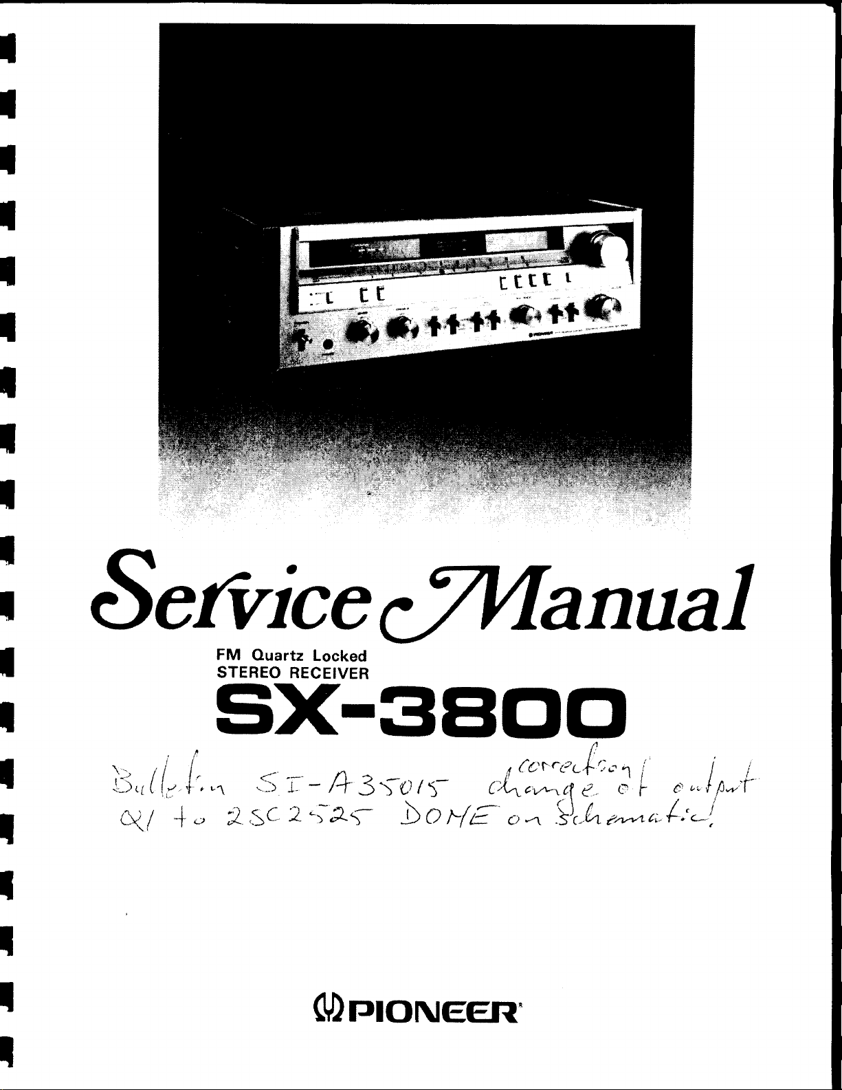
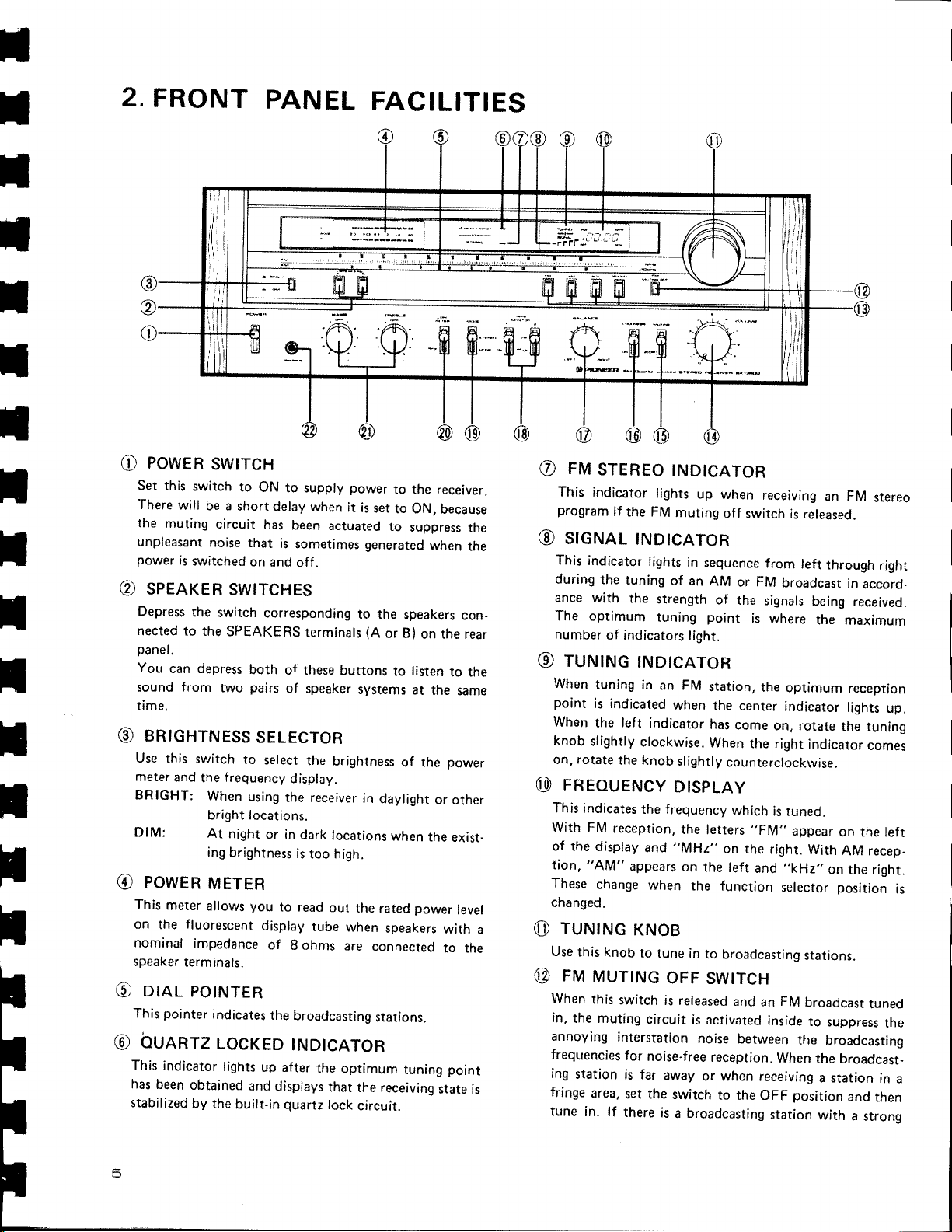

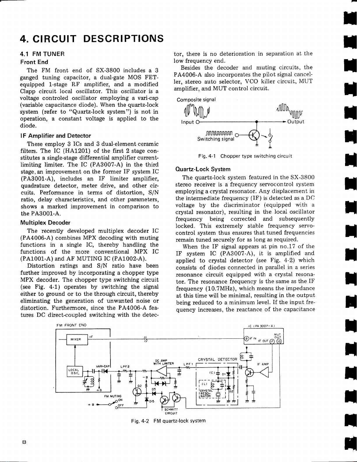
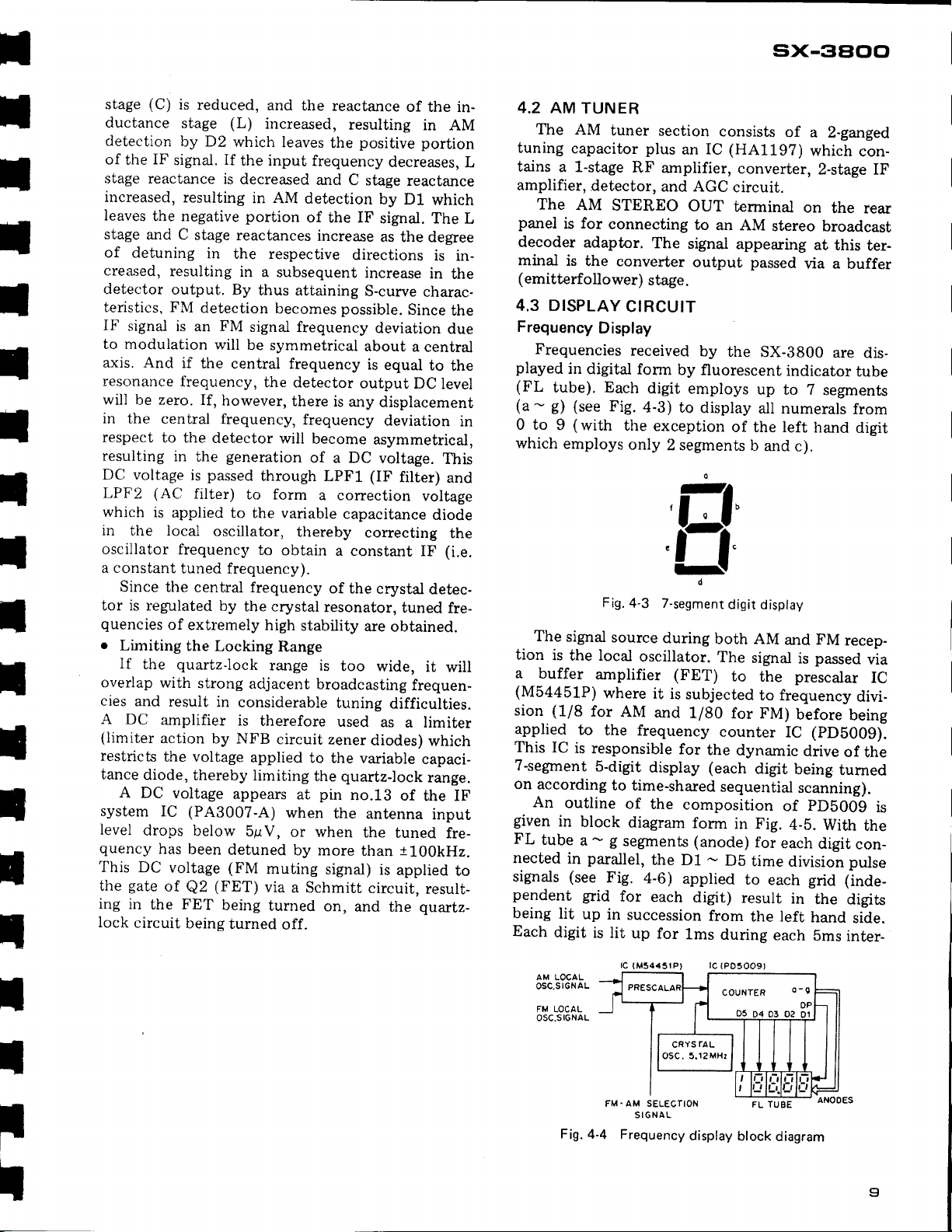
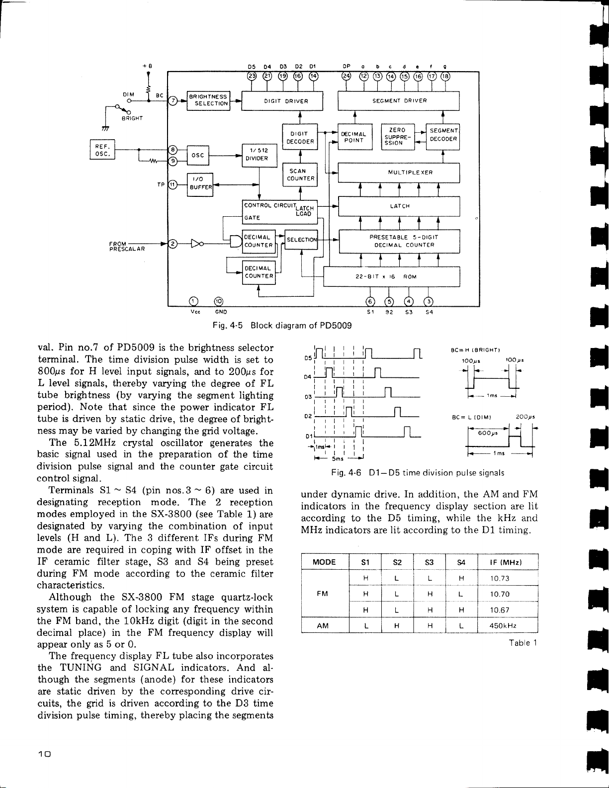
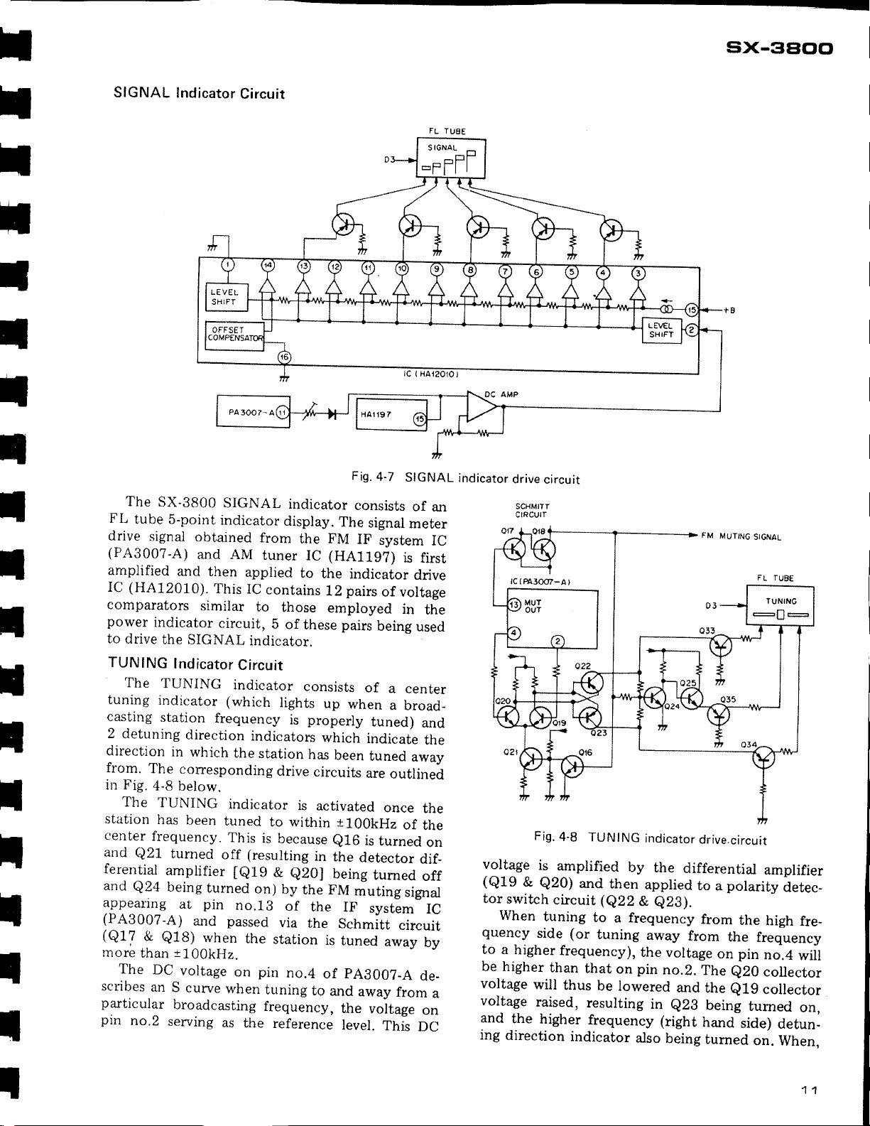
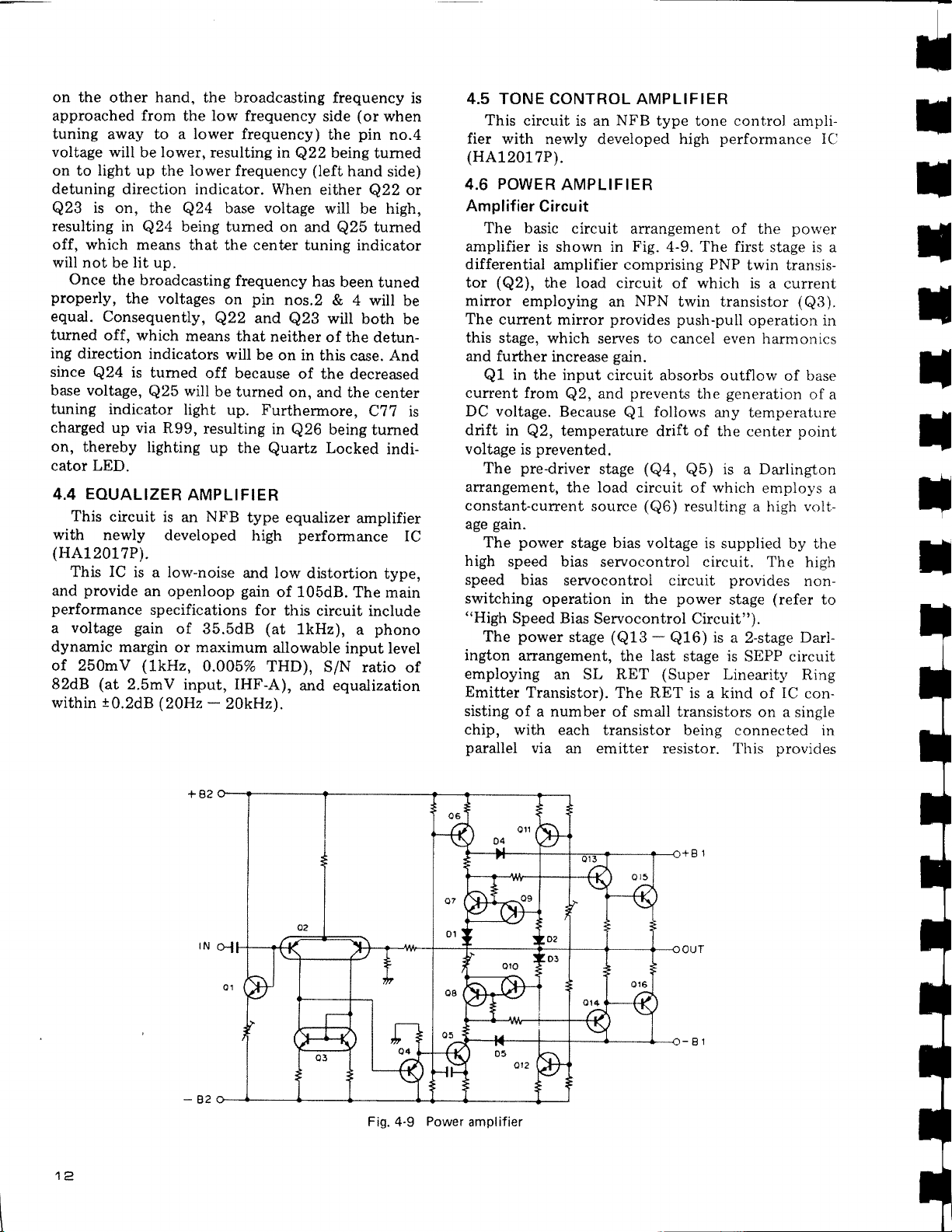
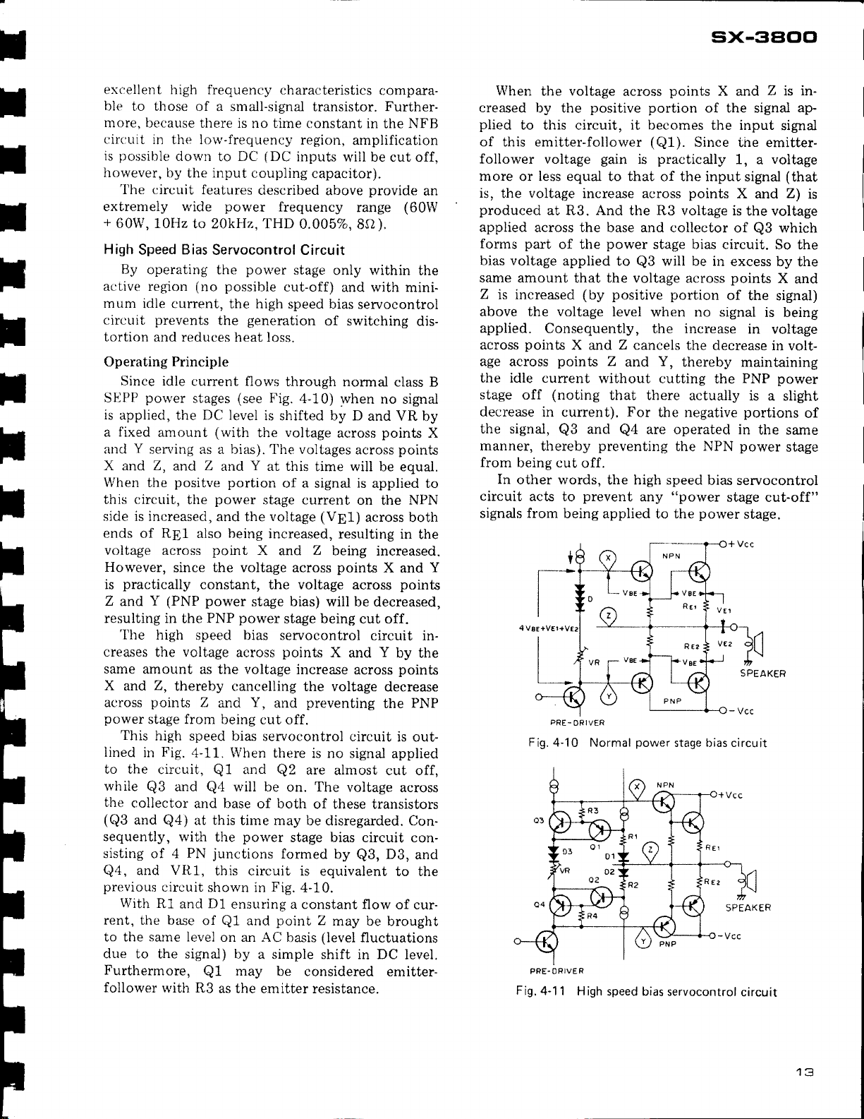
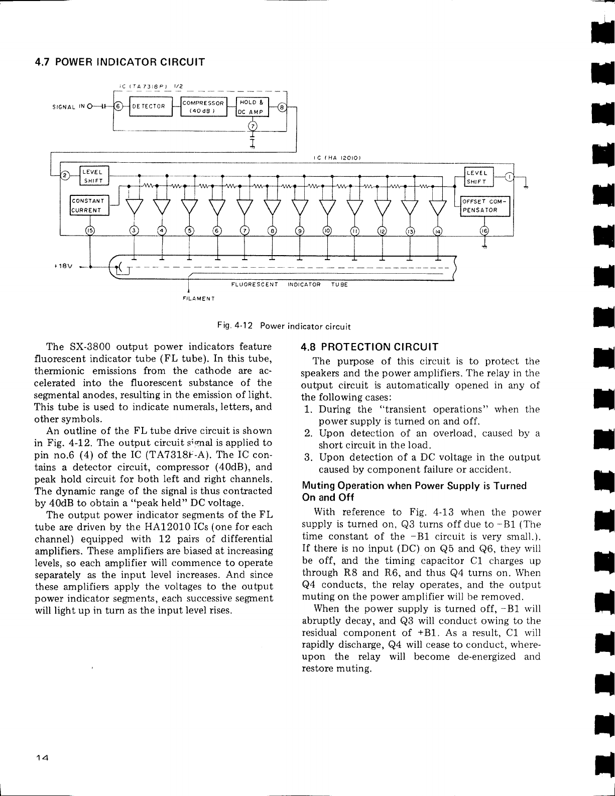
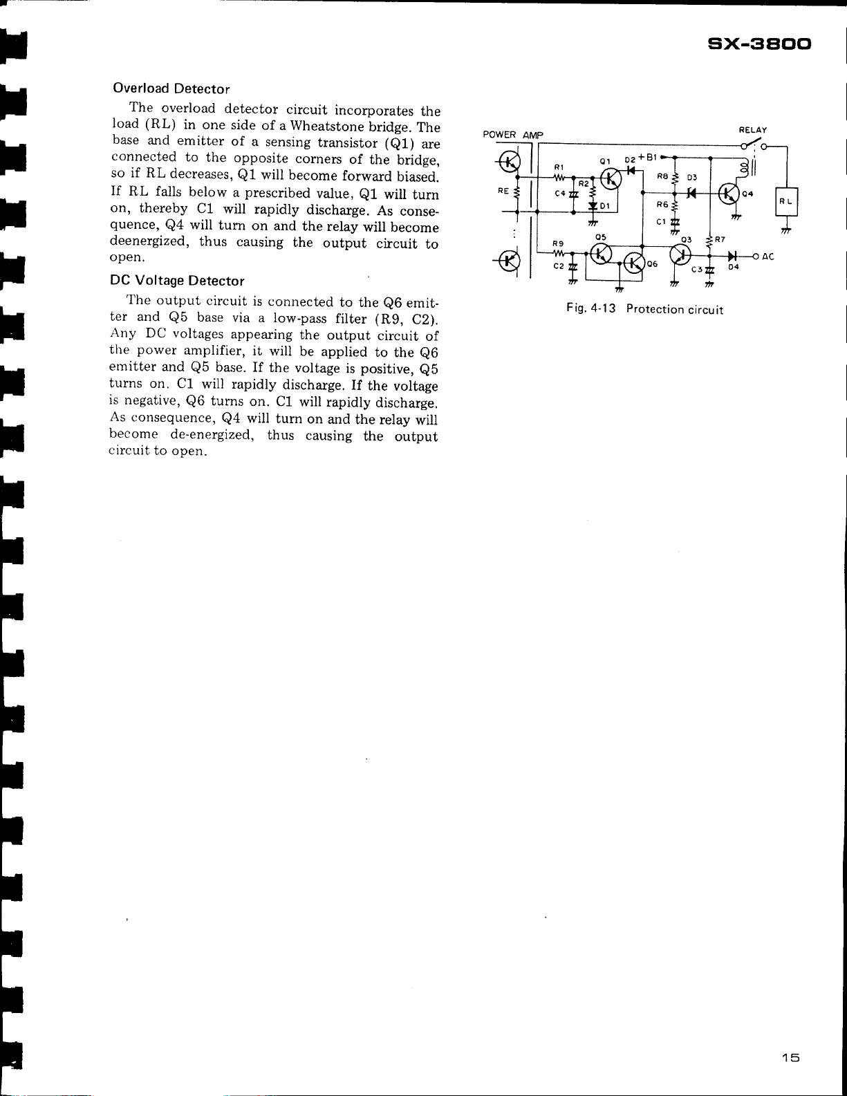
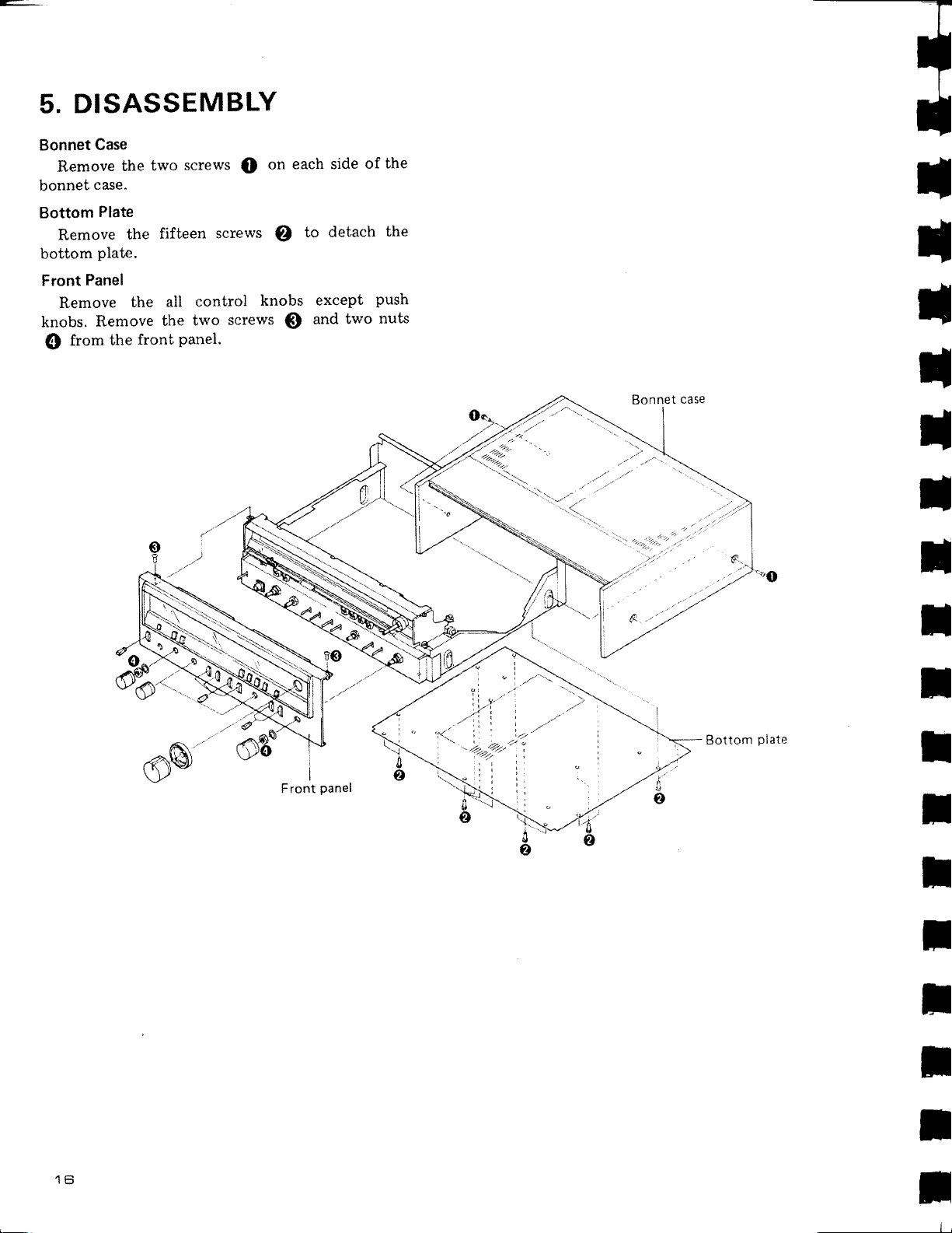


 Loading...