

Pioneer SX-3700, SX-820 Service manual
,a
rilf
EefvicecTlanual
a
STEREO
RECEIVER
sSx-37cIcI
sx-8ecl
()rqoru€Err
MODEL SX-3700
COMES
IN FOUR VERSIONS DISTINGUISHED AS FOLLOWS.
Typ. Voltag.
KU 120V only U.S.A. model
'|
20V only Can€da
11OV
12OV
,
1 1OV . 12OV
is applicable
end 24OV
,22OV ,
22OV , and 240V
,
(Switchabls)
(
Switcha
ble )
to the SX-3700/KU.
Gen€ral
U.S. Military mod6l
For
e
KC
This
service manual
refer
to the additional service manual.
CONTENTS
1. SPECTF |CATTONS
FRONT
2.
3. BLOCK DIAGRAM
4.
CIRCUIT DESCR IPTIONS
4.1 FM Tuner
4.2 AM
4.3 Display
4.4 Equalizer
4.5
4.6 Power Amplif
4.7 Power Indicator
4.8 Protection
DISASSEMBLY
5.
6. PARTS
PANEL FACILITIES
Tuner
Tone Control Amplifier
LOCATION
...........
Circuit . .
Amplif ier
ier . . .... ...
Circuit .. -.
Cirorit . . . . . . -.
......
. , . .
. . . . . . .
. . . .
2
..4
..6
..8
. 11
11
.
11
.
11
.
11
.
13
.
.14
7. DIAL
8. ADJUSTMENTS
8.1
8.2
8.3
8.4
9. SCHEMATIC DIAGRAMS, P,C. BOARD
CONNECTION DIAGRAM AND
LIST
9.1 Schematic
9.2 P.C. Board Conneaion Oiagram . . .
9.3 PansList.....
1O. PACKING
11. EXPLODEOVIEW....
12. ADDITIONAL
Ramarks
model
exDort model
servicing of the other
STRINGING
CORD
FM
Tuner
AM
Tuner
ldle
Current Adiustment
FL
IndicatorCircuit
Diagram
SERVICE
...
.
MANUAL SX.82O
types,
-.......
PARTS
please
......16
41
l'
17
18
19
19
21
za
30
34
J5
l
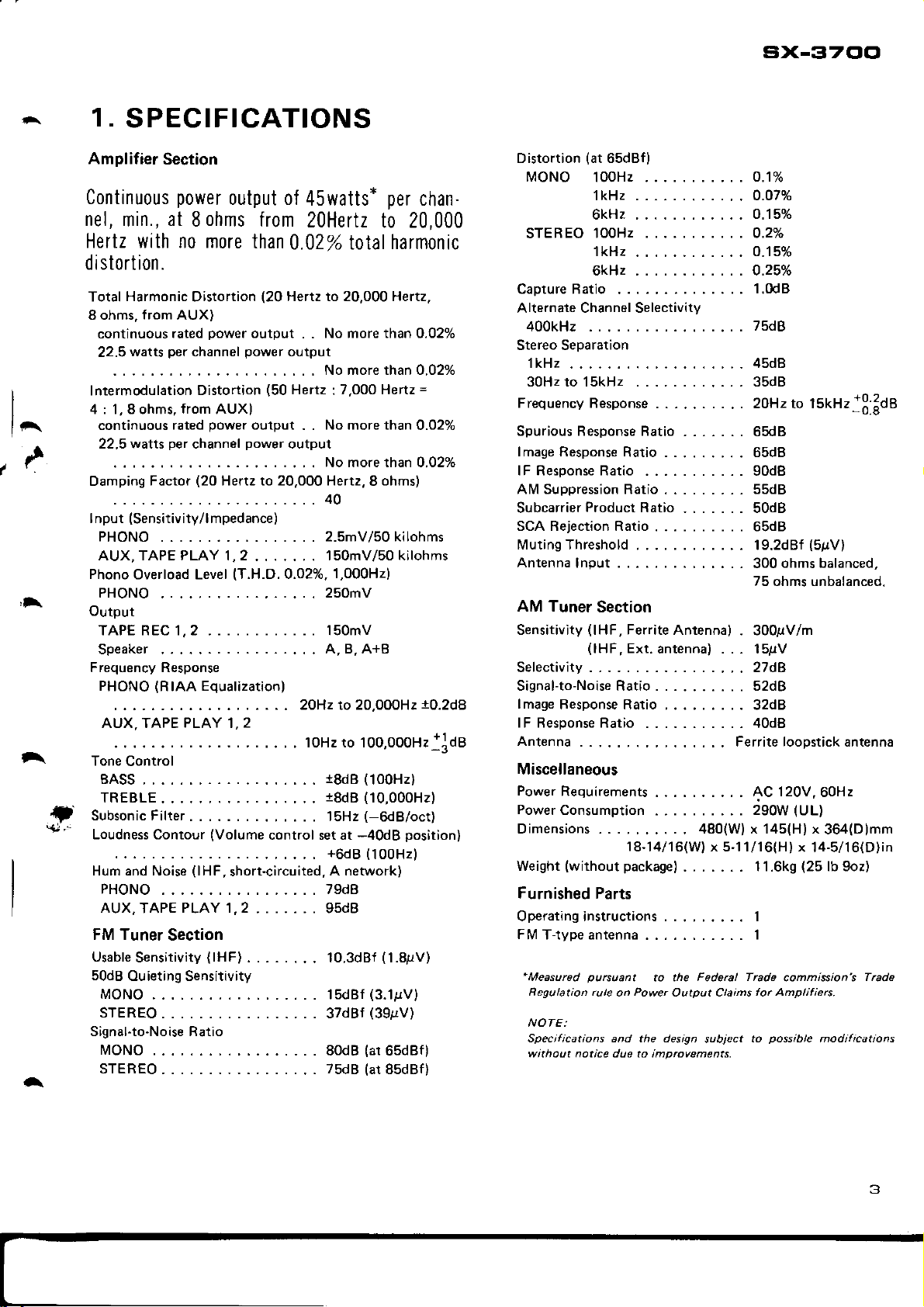
1.
SPECIFICATIONS
six-37C'c'
A
t
,A
A
A
Amplifier
Continuous
nel,
Hertz with n0 more
Section
at 8 ohms
min.,
power
output of
45watts-
from
20Hertz
than0.0?%
d i stort ion .
Harmonic
Total
8 ohms,
Intermodulation
4 : 1, 8 ohms,
Damping
f rom
continuous
per
watts
22.5
continuous
22,5 watts
per
Factor
AUX)
rated
from
rated
Oistortion
Dower
channel
Distortion
oower
channel
(20
(20
Hertz to 20,000 Hertz.
outout
power
AUX)
output
power
Hertz to 20,000 Hertz, S ohms)
. .
output
......
(50
Hertz : 7,0O0 Henz
. .
output
...... Nomorethan0.02%
,"o,irs"",i,i"'ir),;;";;;";;
PHONO
AUX,TAPEPLAY 1,2
Phono
PHONO.
Output
TAPE REC 1,2 -.. .
Speaker
Frequency Response
PHONO
AUX, TAPE
Tone Control
BASS
TREBLE.
Subsonic Filter
Loudness Contour
Hum and Noise
PHONO
AUX,TAPE PLAY 1.2,.
FM Tuner
Usable
50dB
MONO
STEREO
Signal-to-Noise Ratio
t\40No
STEREO,
.
.......'l50mv/50kilohms
Overload Level
.
(R
IAA
PLAY
,,.
. ........79d8
(T.H.O.0.02%,
Equalization)
2
1,
(Volume
(lHF,
control set at
......
short-circuited.
. . 20Hz to 20.000H2
. . .
.....
.....
.....
..... 95dB
Section
Sensitivity
Ou ieting Sensitivity
..
.
(lHF)
. . .
.
.
lOHzto IOO,OOOHZ]]dB
per
chan.
to 20,000
harmonic
total
No more than 0.02%
Nomorethan0,02%
=
No more than
0.02%
""
2.5mV/50 kilohms
1,000H2)
250mV
l50mV
A, B, A+B
10.2d8
(100H2)
iSdB
(10,000H2)
iSdB
(-tuB/oct)
15Hz
-40d8
+6dB{100H2)
A network)
10.3dBf
15dBf
37dBJ
80dB
75dB
position)
(1.8pV)
(3.1l]V)
(39pV)
65dBf)
{at
(at
85dBf)
Distortion
MONO
STEREO
Capture Ratio
Alternate Channel Selectivity
400kHz.
Stereo Separation
l kHz
30Hz to l5kHz
Frequency Response
Spurious Response Ratio
lmage Response
lF Response Ratio
AN4Suppression Ratio.
SubcarrierProductRatio .. . . . .
SCA Rejection Ratio.
Muting Threshold
Antenna
AM Tuner
Sensitivity
Selectivity
Signal-to-Noise Ratio. ......
lmage
lF Response Ratio
Antenna.
(at
65dBf)
l00Hz ........
1kH2.........
6kHz.........
,IOOHZ
1kHZ.........
6kH2.........
.
..... .
Ratio ...
. . .
Input
. . .,.
.. . . ...
.. . . . . . .
Section
(lHF,
Ferrite Antenna)
(lHF,
Ext.
antenna) . .
Besponse Ratio,....
. . .
o.'t70
o.o7./"
0.15%
o.2y,
o.15%
o.25%
1.ft8
75d
B
.45d8
.35d8
. 2OHz to lskHz]3
. 65dB
.65d8
.90d8
.55dB
. 50dB
.65dB
. 19.2dBf
. 300
75
. 300rrV/m
.. 15pV
27dB
..
52dB
. .
. .
. . .
. . 32dB
. . 40d8
Ferrite loopstick antenna
(spv)
ohms balanced,
ohms unbalanced.
3dB
Miscellaneous
Power
Requirements
PowerConsumption
Dimensions .. 480(W) x 145(H) x364(D)mm
Weight
(without
..........
... .....
18-14/16(W)
package)
AC 120V.60H2
290W(UL)
x 5-11/16{H)
x 14-5l16(D}in
11.6k9
{25
lb 9oz)
Furnished Parts
Operatinginstructions ...,,.... 1
FMT-typeantenna
*Measured
Regulation
NOTE:
Specifications and the design
without notice due to improvements.
pursuant
tule on
...........
to the
Power
Output Claims
Federal Trcde
subject
1
commission's
for Amplifie6.
possible
to
Trade
modifications
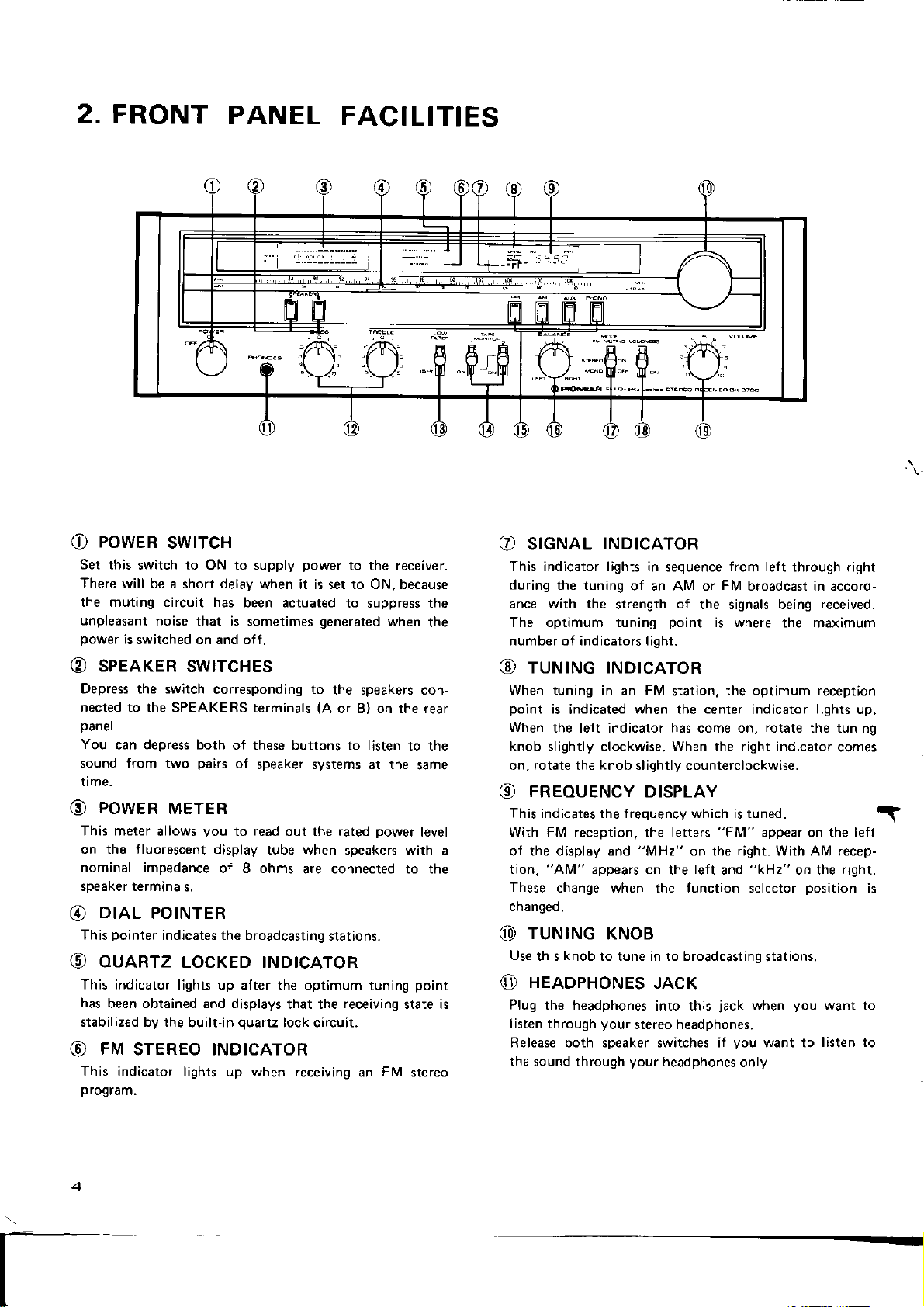
2. FRONT
PANEL
FACILITIES
PowER
O
Set this
There will be a
the muting circuit has
unpleasant
power
SPEAKER
@
Depress the
nected to
panel.
You
can depress both
sound from
time.
POWER
@
This meter
on the fluorescent display
nominal impedance
speaker terminals.
DIAL
O
pointer
This
ouARTz
@
This indicator
has
been obtained
stabilized bv the
FM
@
This indicator
program.
swrrcH
switch to ON to supply
delay
short
noise that is
is
switched on and off.
swITcHEs
switch corresponding to
the SPEAKERS terminals
of these buttons to listen
pairs
two
METER
you
allows
POINTER
indicates the broadcasting
LocKED rNDrcAToR
lights up after the optimum
STEREO INOICATOR
lights up when receiving
to
of I ohms
displays
and
built-in ouartz lock circuit.
power
to the
when it is set to ON. because
been actuated
sometimes
oi
speaker systems at the
read
out the rated
tube when
that the
to suppress the
generated
the speakers con-
(A
or B) on the rear
speakers with a
are connected to the
stations.
receiving
power
tuning
FM
an
receiver.
when
the
to the
same
level
point
state is
stereo
SIGNAL
@
This indicator lights
during
ance with the
The optimum tuning
number of indicators light.
TUNING INDICAToR
@
When
tuning in an FM
point
is
When
the left indicator has come on,
knob
slightly clockwise. When the right indicator
rotate
on.
FREOUENCY
@
This indicates the frequency which is tuned.
With FM reception,
of the display and
"AlV"
tion.
These
changed.
TUNING
@
Use
this
HEADPHONES
O
Plug
the headphones
listen through
Release both speaker switches ii
the
sound through
INDtcAToR
in sequence
the tuning
indicated
the
of an AM or
strength of the signals being received.
point
station.
when the
knob
slightly counterclockwise.
DISPLAY
the letters
"MHz"
appears
change when the function
on
the
KNOB
knob
to tune in to broadcastinq
JACK
into this
your
stereo headphones.
your
headphones
from
FM
is where
the optimum reception
center indicator
"FM"
on the right. With AM recep-
left
and
jack
you
broadcast in
appear on the left
"kHz"
selector
when
want to
only.
left through right
accord-
the maximum
lights
up.
rotate
the tuning
comes
on the
stations.
you
right.
position
want to
listen to
T
is
six-37clcl
]^
.r.
\A
a
q}'..
BNSS AND TREBLE
@
Use these controls to adjust the bass
turn the bass control to the
you
tion,
frequency range. Conversely,
left
You
high-trequency range.
@
When this switch is
can
that
which is
table and other
cannot be heard, it can
tion and damage the
@
Employ for tape
progress.
1: Playback or monitoring of a tape deck connected
2:
NOTE:
L Be sure to set the switches to the uppet
2. When lecording with two tape decks
@
Depress the function
program
before selecting a different function
sound
FM:
AM:
AUX:
PHONO:
NOTE:
Only one function switch should be deptessed at a time.
will be able to emphasize the sound in
from
the center
can use the treble
LOW
rape
FILTER
provided
be
you
can cancel out noise in the ultra-low frequencies
generated
MoNtroR
the TAPE 1
Playback
the TAPE
playing
when
opefate the tape monitor I switch as
signal to the TAPE 2 deck.
(0)
SWITCH
set to
for frequencies
by low-pitched rumble from
forms
of distortion. Although this noise
speakers.
playback
jacks.
or monitoring of a tape deck connected to
2
iacks.
rccords or
FUNCTION SELECTOR
source. Turn the volume control down first
trom
program
one
Depress this switch
Depress this
Depress this
audio component
AUX
Oepress this switch
cord
PHONO
coNTRoLS
and the treble.
right
from itscenter
turning this control to the
position
control
generate
willattenuate the
to adiust
'lsHz.
below 15H2. This means
the sound
a 6dB/oct attenuation
intermodulation distor-
{0)
the
a turn-
swrrcHEs
or to monitor a recording in
(OFF)
position
listeninq to
switch which corresponds to the
source is being reproduced.
jacks.
on the turntable connected to the
iacks.
brcadcasts.
simultaneously,
switch
when listening
switch
will interupt the
this
switch
for FM
for
connected to the
when
while
broadcasts.
AM broadcasts.
playing
you
lf
posi-
low-
sound.
in
the
to
do not
the
to an
re-
a
enlnNce
@
Use
this control
right
channels.
switch
to MONO/OFF.
on the right, it means
higher.
is
Conversely, if the
it
Therefore,
adjust. After adjusting.
switch to STE REO/ON.
@
This
the mode
STEREO/ON
while
interstation
listening
MONO/OFF
mode. while the FM muting function
enabling
tuning in to the FM broadcasting
NOTE:
Recoding
the MONO/OFF
@
When
trol
accentuated.
When
hear
switch is
By depressing
more
the volume control is
@
Use this control
and
put
Turn
means
MODE/FM MUTING SWITCH
switch is a combination of the
the
to
suitable reception of weak radio
LOUDNESS
listening
turned down, depress
the
the bass than when
thus designed to compensate
strongly and the
VOLUME
headphones.
level. No
coNTRoL
to balance the volume
First,
however,
lf the
that the volume
the balance control to
sound appears to be louder
that the volume
turn the balance
select switch.
position
F l\il
muting function acts to suppress unpleasant
noise while tuning between FM
FM
position,
stercophonically
the reproduction is
broadcasting. When
however,
position
may
SWITCH
perlormance
to a
volume
low,
is
this switch, the bass come through much
sound
turned down,
CONTROL
to adjust the output level to
Turn it
sound will be heard if
set the mode/FM muting
sound appears to be louder
of the left channel is higher.
control to the right
return the mode/Fl\4
When setting this switch at
reproduction is in mono
station.
with
the
the
mode/FM muting
the
cause deteriorction in channel se-
this switch and the bass
human
volume is high.
takes on a
clockwise to increase the
of the left and
right
ot the
the left and adiust.
F l\il muting
jn
setting this switch at
does not act, thus
with the
finds
ear
for
this deliciency.
punch
you
set
channel
on the leJt,
muting
switch and
mode,
stereo
stations
stations
volume
The
it
when
when
swiach
will
it harder to
loudness
even when
the speakers
"0."
to
and
in
con-
be
out-
5
BLOCK
3.
RF
Block
STEREO
AM
OUT
DIAGRAM
(NAt201)
c
]NOICATOR IUEE
AF Block
t;
REC F.AY R€C PLAY
R
CHANNEL ( SAME
AS
L CHANNEL)
r$
SPEA(ER B
HEAo
ll
a i,BfffiJ*
G)
o
r
six-37ClC'
-)A
-\-A
4.
CIRCUIT
4.1 FM TUNER
Front End
FM front
The
ganged
equipped 1-stage RF
Clapp circuit
voltage controled
(variable
system
operation, a constant
diode.
lF Amplif
filters. The IC
,)
stitutes a
limiting
stage,
(PA3001-A),
quadrature
cuits.
ratio, delay
shows a marked improvement in
the
Multiplex Decoder
(PA4006-A)
functions in a
functions
(PA1001-A)
further improved by incorporating a chopper
MPX
(see
either to
t
eliminating the
distorition. Furthermore, since the
tures
tuning capacitor, a dual-gate
local oscillator. This oscillator is
capacitance diode). When the
(refer
These employ 3 ICs
an
Performance in terms of distortion,
PA3001-A.
The recently developed multiplex
Distortion
decoder.
Fig. 4-1) operates by switching
DC
to
ier and Detector
(HA1201)
single-stage differential amplifier current-
limiter. The IC
improvement on the
includes an IF
detector, meter drive, and
characteristics, and other
combines
of
the
and AF MUTING
ratings
The
ground
generation
direct{oupled
DESCRIPTIONS
of
end
oscillator employing a vari-cap
"Quartz-lock
single IC, thereby
more conventional
chopper type
or to
SX-3700
amplifier, and a modified
voltage is applied to
and 3 dual-element ceramic
of the first 2 stage con-
(PA3007-A)
former IF system IC
MPX
decoding
S/N ratio have been
and
the through circuit, thereby
of
switching with the detec-
includes a 3
MOS EFT-
quartz-lock
system") is not in
in
the third
limiter amplifier,
other cir-
parameters,
comparison to
decoder
lvith muting
handling the
MPX IC
(PA1002-A).
IC
switching circuit
the signal
unwanted nois€ or
PA4006-A fea-
the
S/N
IC
type
at the
circuits,
signal cancel-
the
MUT
and
VCO
ctcuit.
separation
in
muting
pilot
the
killer circuit,
there is
tor,
frequency end.
low
Besides
PA4006-A also incorporates
ler, stereo
a
amolifier. and
Composite
no
deterioration
decoder
the
auto selector,
MUT
control
signal
4l1i\r1l''
InoutffiOutOut
-ri:-'',
JlIlIl[JlIUUrn ^---a
s* iiit''i'iri
4-1 Chopper type switching circuit
Fig.
Ouartz-Lock System
quartzJock system
The
stereo receiver is
employing
in the
DC voltage by
crystal resonator),
frequency
locked.
control system
remain
When
IF system
applied
consists
resonance
tor.
frequency
at this time
being
quency
a crystal
intermediate
This extremely
tuned securely
the IF signal
to crystal
of diodes
clcuit equipped
The resonance
(10.7MH2),
reduced
increases,
a frequency
the discriminator
being
thus ensures
(PA3007-A),
IC
will be
to a minimum
the
"--\y'
i r
featured in
resonator.
frequency
resulting in
conected
stable
that tuned
long as required'
for as
appears
detector
connected
frequency is
which
minimal, resulting
reactance
i
-
7
,,T
SX-3700
the
servocontrol
Any displacement
(IF)
is
(equipped with a
the local
and
frequency
pin
at
is amplified
it
(see Fig.4-2) which
parallel
in
with a crystal
the same
means the
level. If
of the canacitance
system
detected
subs€quently
frequencies
no.17
impedance
in the
the input
as a
oscillator
servo-
of the
and
in a series
resona-
as the
output
fre-
IF
----f::,
-"
'''i'ill
(!r
t5
DETECTOR
r:
I I I
,t
?-J
I
CRYSTAL
|
| +:
t:
;i..*'F--?-'i+r
ITNATOR = rll'
t_-----F-- I | ;
l_
(C)
stage
ductance
detection
of
the IF signal. If the input frequency
L stage reactance is decreased
ance increased,
which leaves
The L stage
the
is
increased, resulting in
the detector
characteristics, FM
Since
deviation
about a central
is equal
output DC level
any displacement
quency
become asymmetrical,
of a DC
LPF1
correction voltage
capacitance diode in
correcting
constant IF
Since
tor is regulated
quencies
r
Limiting the t ocking
If
overlap with strong
cies and result in considerable
A DC amplifier
(limiter
restricts
tance diode, thereby limiting the
A DC
system IC
level drops below
quency
This
the
ing in the FET
lock circuit being
4.2
The AM
capacitor,
transistor
(converter),
4.3 DISPLAY
Frequency
Frequencies
is reduced,
stage
by D2
the negative
and C stage reactances
degree of detuning in the respective
output. By thus attaining
IF
the
to the resonance frequency,
deviation
voltage. This DC voltage
(IF
the central frequency
the
action
the
has
DC
gate
of
signal is an FM signal
due
to
filter)
the
(i.e.
of extremely high
quartzJock
by
voltage
voltage appears at
(PA3007-A)
been detuned by more
voltage
(FET)
Q2
and the
(L)
increased,
which leaves the
resulting in AM detection by D1
detection
modulation it will
axis. And if the central frequency
will be zero. If, however,
in the central
in respect to
resulting in
and LPF2
which is applied
the
oscillator
a constant
by the crystal resonator,
Range
range
adjacent broadcasting frequen-
is therefore used as a limiter
NFB
circuit zener
applied to the variable
SpV, or when the tuned fre-
(FM
muting
via
being turned on, and
tumed off .
reactance
and C stage react-
portion
a subs€quent increase in
becomes
(AC
local
oscillator,
frequency
tuned
of the crystal det€c-
stability
is too wide, it
tuning
pin
when the antenna
signal) is applied
a Schmitt circuit, result-
AM TUNER
tuner stage
a singleclement
RF amplifier, a PNP
and an NPN transistor
CIRCUIT
Display
received
employs a
ceramic filter,
by
the SX-3700 are
of the in-
resulting in AM
positive portion
decreases,
of the IF signal.
increase as
directions
S-cuwe
possible.
frequency
symmetrical
be
the
detector
there is
frequency, fre-
detector
the
generation
the
passed
is
filter)
frequency).
quartz-lock
no.13 of the IF
to form a
to the variable
to obtain a
tuned fre-
are obtained.
difficulties.
diodes) which
than 1 100kHz.
the
will
through
thereby
will
capaci
range.
input
quartz-
2-ganged tuning
NPN
an
transistor mixer
IF amplifier.
dis-
to
played
tube
ments
from 0
digit which
in digital
(FL
-
(a
to 9
tube). Each digit employs up to 7 seg-
g)
employs
form
(see
Fig.
(with
the exception of the left hand
only 2
fluorescent
by
4-3) to display all numerals
segments b and c).
Lt
ti
d
Fig. 4-3
The
signal source
tion is the local oscillator.
a buffer
(M54451P)
sion
applied to the frequency
This IC is responsible
?-segment 5-digit
on according to
An outline of the
given
FL
tube a
nected in
signals
pendent
being lit up
Each
osc,sr6NAL
OSC.SIGNAL
val. Pin
terminal. The time
8009s
level signals,
L
tube
period).
tube
ness may
The
basic signal used
division
control
amplifier
where it is
(1/8
for AM and 1/80 for FM)
in block diagram form
-
g
segments
parallel,
(see
Fig. 4-6)
grid
for each digit) result
in succession from the left hand
digit is lit up for
Fig.
4-4 Frequency
no.7 of PD5009
for H
brightness
is driven by static drive, the degree of bright-
level input signals,
Note
varied
be
5.12MHz crystal oscillator
pulse
signal and the counter
signal.
7-segment
during both AM and
(FET)
subjected to
for the dynamic
display
time-shared sequential
composition of
D1 - D5
the
applied to each
1ms during each 5ms
sr.NAL
division
thereby varying the degree of FL
(by
varying the segment lighting
that since the
by changing the
in the
display
The signal is
to the
frequency
counter IC
(each
(anode)
display block
is the brightness selector
preparation
digit being
Fig. 4-5. With
in
for
each digit con-
time
division
in the digits
FL luB€
diagram
pulse
width is set to
and to 2009s
power
indicator
grid
generates
indicator
FM
recep-
passed
prescalar
before being
(PD5009).
drive of the
scanning).
PD5009
grid
voltage.
of the time
gate
via
IC
divi-
tumed
the
pulse
(inde-
side.
inter-
for
FL
the
circuit
is
r
sx-37c'cl
l;
(^,
\
t,
+1,.
Terminals S1 - 54
designating reception
modes
designated
levels
mode are required
IF
during
employed in the SX-3700
by varying the
(H
and L). The 3 different IFs during
in coping with IF
ceramic
filter stage, S3
FM mode according
(pin
nos. 3
mode.
combination
-6)
are used in
The 2 reception
(see
Table 1) are
offset in the
54 being
and
to the
ceramic filter
of input
FM
preset
characteristics .
Although the SX-3700
FM stage
quartzJock
system is capable of locking any frequency within
the FM band, the 10kHz digit
decimal
place)
in
FM frequency display will
the
(digit
in the second
appear only as 5 or 0.
The frequency
the TUNING
display
and
though the segrnents
are static
cuits, the
division
driven by the
grid
is
driven according to
pr:lse
timing,
Fig.
4.6 D1.D5 time division
FL tube also incorporates
SIGNAL
(anode)
indicators. And al-
for
these indicators
corresponding drive cir-
the D3 time
thereby
placing
gC=
H
pulse
the segments
(ARIGHT,
signals
PRESETABLE
OECIMAL COUNTER
22-BlT r 15
under
dynamic drive. In addition, the AM and
indicators in the frequency
according to the Db timing,
MHz
indicators are lit according to the
MODE st
H H 10.73
H
H
L
TUNI NG Indicator
The TUNING indicator
tuning indicator
casting
2
station
frequency
detuning direction indicators
5-OIGIT
ROM
s2
L
L
H L
Circuit
(which
lighLs up when a broad-
display section are lit
while the
s3
H
H H
consists of a center
properly
is
which
direction in which the station has
from. The corresponding
lined in Fig.
The
station has
center frequency.
and
Q21
ferential amplifier
and
Q14
signal appearing at
(PA3007-A)
(Q15
more
than
4-7.
TUNING indicator
been tuned to
This is because
(resulting
tumed
off
IQ19
being tumed
pin
passed
and
&
when the station is tuned away by
Q16)
t
100kHz.
drive circuits are out-
activated once
is
within
in the detector dif-
&
Q20l
on) by the
no.13 of the IF system IC
via the Schmitt
FM
kHz
and
D1
timing.
s4 lF
{MHz)
't0.70
'r0.67
450k Hz
Table
tuned)
and
indicate the
been tuned away
t
100kHz of
is tumed on
Q22
being tumed off
FM
muting
circuit
1
the
the
The DC voltage
scribes
a
pin
voltage
(Q19
tors switch
an S
particular
no.2
serving
is amplified by
&
Q20)
SCHMiTT
curve when tuning
broadcasting
circuit
pin
on
frequency,
as the reference
the differential
and then
(Q16
applied
&
Q26).
no.4
of PA300?-A
to
to a
and
away from
the voltage
level.
This DC
amplifier
poladty
de-
on
detec-
and
the higher frequency
ing direction
on the other hand, the broadcasting frequency
approached from the low frequency
tuning away to a lower frequency) the
voltage
on to light up the
detuning
is on, the
Q26
resulting in
off,
which
not be lit up.
will
Once the broadcasting frequency has been tuned
properly,
equal.
turned off, which means that neither of
ing direction indicators will be on in this case. And
since
Q14
base voltage,
tuning indicator light up.
charged up via R84, resulting in
on, thereby lighting up the
cator
LED.
indicator
will be
Consequently,
lower, resulting
lower
direction indicator.
Q14
being turned on and
Q14
means that
voltages
the
is turned off because of
will
Q18
(right
hand
also being
frequency
base voltage
the center tuning
on
Q16
be turned
turned on.
side
in
Q16
(left
When
pin
and
Furthermore,
Quartz
either
will be
nos.2 & 4 will be
Q26
the decreased
on, and
Q23
side) detun-
When,
(or
when
pin
no.4
being turned
hand side)
or
Q16
high,
turned
Q18
indicator
will both be
the detun-
the center
C16
tumed
being
Locked indi-
is
is
Fig.
4-7 TUNING indicator
When
quency
to a
be
voltage will thus
voltage raised, resulting
tuning to a frequency from
(or
higher
higher
side
than that on
tuning away from
frequency),
pin
be lowered and the
voltage
the
no.2. The
in
Q26
driver
circuit
the
the frequency
pin
on
Q20
Q19
being
turned on,
high
fre-
no.4 will
collector
collector
SIGNAL Indicator
The
SX-3700
FL
tube
5-point indicator
drive
signal obtained
(P43007-A)
then applied
This IC
similar to
circuit, 5 of
SIGNAL indicator.
contains
those employed
SIGNAL
and AM
to
the indicator drive
12
these
Circuit
indicator consists
display. The signal
from the FM
tuner is first amplified
pairs
of voltage comparators
in the
pairs
being used to
IF system IC
IC
power
of an
meter
and
(HA12010).
indicator
drive the
r
Fig. 4-8
SIGNAL indicator driver circuit
F
EOUALIZER AMPLIFIER
4.4
NFB
This circuit
with
(M5214L-P).
and
performance
a voltage
dynamic
of 250mV
79dB
within t 0.2dB
4.5 TONE CONTROL
fier with newly
(M5214L-P).
4.6
amplifier. The
(Q3),
employing an
rent mirror
stage, v/hich
harmonics
circuit
provides
complementary
of 45W
O.O2%,2OHz-2OkHz\.
newly developed
This IC
provide
(at
circuit
This
POWER
This is the basic circuit
the load circuit of which
pre-driver
The
(D5,
power
The
is an
is a low-noise and
openloop
an
specifications
gain
margin or maxirnum
(lkHz,
2.5mV
AMPLIFIER
provides push-pull
and
Q11),
voltage
high
(8O
load. at both
35.5dB
of
O.O2Vo
input, IHF-A),
(2OHz
is
NPN
serves
further increase
stage
-
NFB type tone
an
developed
first stage is a differential amplifier
twin
stage
enables
gain.
is a
SEPP ctcuit,
equalizer amplifier
type
performance
high
low distortion
gain
2OkHz).
AMPLIFIER
transistor
to
(Q7)
Darlington connection
105dB. The main
of
for this circuit include
(at
lkHz), a
allowable input
THD),
high
arrangement of
cancel even
with a current
stable operation
channels driven,
S/N ratio
and equalization
control ampli-
performance IC
is
a current
(Qb).
operation
gain.
and
The cur-
numbered
has an output
IC
type,
phono
level
power
mirror
in
this
mirror
and
pure
THD
of
POWER INDICATOR CIRCUIT
4.7
The SX-3700
fluorescent
thermionic
celerated
segmental anodes,
This tube
other symbols.
An
Fig.
in
pin
tains a detector
peak
The
40dB to obtain a
by
The output
tube are driven
channel)
amplifiers.
ing levels, so
operate
since these amplifiers
put power
segment will
rises.
4.8 PROTECTION CIRCUIT
In order to
speakers,
protection
automatically
As can be seen
of 3
into the
is used to
outline of the
4-9.
(4)
no.6
hold circuit for
dynamic range
equipped with
separately
the SX-3700
main component
output
indicator tube
emissions
resulting in
The output
of the
circuit,
power
by the
These amplifiers
each amplifier will
as the input
indicator
light up in tum
protect
circuit which
by a relay
from
power
(FL
from
fluorescent substance
indicate numerals.
FL tube drive circuit
circuit signal is
(TA7318P-A).
IC
compressor
both left and
of the signal is
"peak
held"
indicator segments
HA12010 ICs
12
apply the
segments, each
both the amplifier
has been equipped
is opened and
Fig. 4-11, this circuit
parts.
Eix-37c'Cl
indicators
tube).
the
the emission
pairs
are biased
level increases.
in the output
In this
cathode
letters,
applied to
The
(40dB)'
right channels.
thus contracted
DC voltage.
(one
of differential
at increas-
commence
voltage to the out"
successive
as the input
feature
tube,
are ac-
of the
of light.
and
is shown
IC con-
and
of the
for each
And
level
and the
with a
closed
circuit.
consists
FL
to
T^
fD
(fafatSP)
)c
OE
TECIOR
t/2
gE
FLUORESCEN
Fig. 4-9 Power indicator circlrit
I ]NDICAIOR
TU
ac
7 .2v
The relay
delaying
on, opening
tumed
to instructions
power
the
via R8,
across
difference
on due
the
off, C4 is
ing
being opened.
10 below consists
load
by the
opposite comers
value
be
on
charged
tumed
the capacitor
relay contacts.
in
The overload
RL
drops
tumed on
C4
drive circuit
relay
closure
the relay
off, and
thereby increasing
to
Q6
forming
potential
in
via
off and
a.lso opening the relay
from
is first switched
exceeds
the forward
discharged rapidly
being
detector circuit
below a
due to forward
the relay
D3
the relay contacts
controls relay operation,
when the
quickly
each detector
terminals. Once
the zener diode,
When the
tumed off and
of a Wheatstone
one
of the arms.
difference
of the bridge
certain fixed level,
drive circuit
and
Q3,
when the
on,
potential
the
biasing, thereby closing
via
betyyeen
biasing. The charge
resulting
power
C4
power
Db
the relay contacts
outlined in Fig. 4-
circuit. If
is switched
power
in response
circuit.
is
this
Q6
and
bridge with
Q3
diametrically
will thus be dis-
in
being opened.
When
charged up
difference
potential
is turned
is switched
result-
R7,
the
is
biased
the RL
will
Q3
being
Q6
If for
the output, it
is
detector
being
Rb
normal signal
application
and
output, it is
to
Q4
to
the
of
be tumed
ly,
Q6
opened. If
output,
while
since a negative
Q5
contacts
any reason a DC voltage
will be detected
circuit, resulting in
opened to
and C2 form a low-pass
of signal voltages
If
Q5.
and
ground,
reverse bias
Q4
the base of
being turned
Q5
in
this situation,
a
Q5.
this transistor
is
connected
on due to a forward
a negative DC voltage
is tumed
Q4
is
tumed on due to a forward
ooened.
thereby
components,
positive
divided by
Since the
applied.
Q6
voltage is
DC voltage
ground,
to
grounded
is
off and the
off due to a reverse
is tumed
Q6
R5 and R6, and applied
the relay
protect
filter
thereby
to
base of
will remain off
And since the emitter
by
relay contacts
applied to the
generated
is
by the DC voltage
contacts
the speakers.
designed to block
preventing
the bases of
appears at the
is connected
Q5
this transistor
bias.
Consequent-
resulting in
Q4,
appears at the
bias.
emitter of
off and the relay
at
the
Q4
due to
will
being
bias,
And
Fig.4-10
Overload
Pow€r
amplifi€r
""*";.;;;l
F|€l€y driv€
Detector
Overload detector
circuit
C ircu it
F
powor
AC
supply
Fig.
circuit
voltag€
DC
dstsctor circuit
l[&'#bfr
ll
J
;.+
|
t:.
R6lay
4-11 Protection
Circu it
driv€
ci rcuit
,l
I
J
4,
 Loading...