

Page 1
PIONEER CORPORATION 4-1, Meguro 1-chome, Meguro-ku, Tokyo 153-8654, Japan
PIONEER ELECTRONICS (USA) INC. P.O. Box 1760, Long Beach, CA 90801-1760, U.S.A.
PIONEER EUROPE NV Haven 1087, Keetberglaan 1, 9120 Melsele, Belgium
PIONEER ELECTRONICS ASIACENTRE PTE. LTD. 253 Alexandra Road, #04-01, Singapore 159936
PIONEER CORPORATION 2004
SE-DIR800C
DIGITAL CORDLESS SURROUND HEADPHONE
SE-DIR800C
THIS MANUAL IS APPLICABLE TO THE FOLLOWING MODEL(S) AND TYPE(S).
Model Type Power Requirement Remarks
SE-DIR800C KUCXCN1 AC120V
SE-DIR800C NYXCN AC220- 240V
ORDER NO.
TRT1133
For details, refer to "Important symbols for good services" .
T-ZZR MAR. 2004 printed in Japan
Page 2
1234
SAFETY INFORMATION
A
This service manual is intended for qualified service technicians; it is not meant for the casual
do-it-yourselfer. Qualified technicians have the necessary test equipment and tools, and have been
trained to properly and safely repair complex products such as those covered by this manual.
Improperly performed repairs can adversely affect the safety and reliability of the product and may
void the warranty. If you are not qualified to perform the repair of this product properly and safely, you
should not risk trying to do so and refer the repair to a qualified service technician.
WARNING
B
This product contains lead in solder and certain electrical parts contain chemicals which are known to the state of California to
cause cancer, birth defects or other reproductive harm.
Health & Safety Code Section 25249.6 – Proposition 65
NOTICE
(FOR CANADIAN MODEL ONLY)
Fuse symbols (fast operating fuse) and/or (slow operating fuse) on PCB indicate that replacement
parts must be of identical designation.
REMARQUE
(POUR MODÈLE CANADIEN SEULEMENT)
C
Les symboles de fusible (fusible de type rapide) et/ou (fusible de type lent) sur CCI indiquent que
les pièces de remplacement doivent avoir la même désignation.
(FOR USA MODEL ONLY)
1. SAFETY PRECAUTIONS
The following check should be performed for the
continued protection of the customer and service
technician.
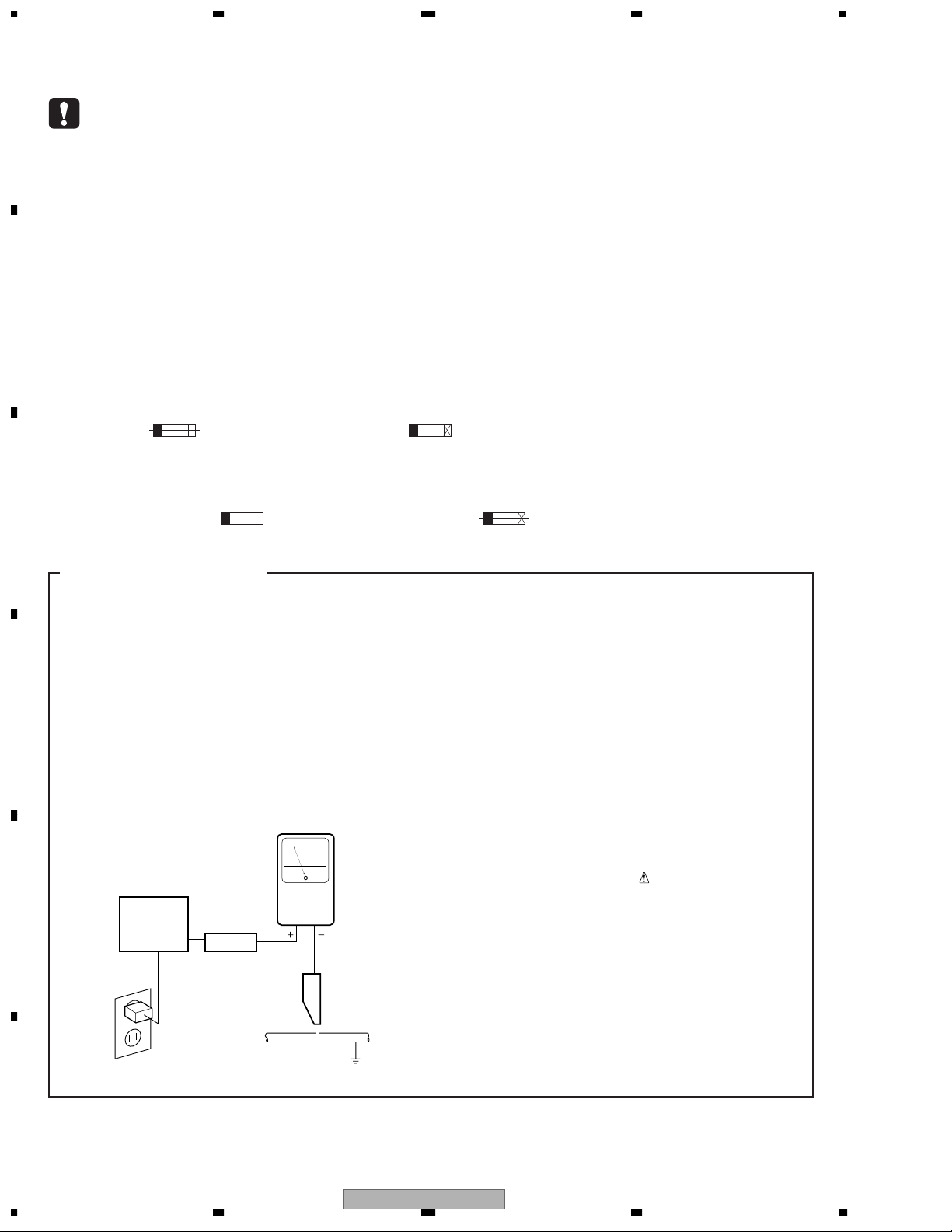
LEAKAGE CURRENT CHECK
Measure leakage current to a known earth ground
(water pipe, conduit, etc.) by connecting a leakage
D
E
current tester such as Simpson Model 229-2 or
equivalent between the earth ground and all exposed
metal parts of the appliance (input/output terminals,
screwheads, metal overlays, control shaft, etc.). Plug
the AC line cord of the appliance directly into a 120V
AC 60 Hz outlet and turn the AC power switch on. Any
current measured must not exceed 0.5 mA.
Reading should
not be above
0.5 mA
Earth
ground
Device
under
test
Also test with
plug reversed
(Using AC adapter
plug as required)
Test all
exposed metal
surfaces
Leakage
current
tester
AC Leakage Test
ANY MEASUREMENTS NOT WITHIN THE
LIMITS OUTLINED ABOVE ARE INDICATIVE
OF A POTENTIAL SHOCK HAZARD AND
MUST BE CORRECTED BEFORE RETURNING THE APPLIANCE TO THE CUSTOMER.
2. PRODUCT SAFETY NOTICE
Many electrical and mechanical parts in the appliance
have special safety related characteristics. These are
often not evident from visual inspection nor the
protection afforded by them necessarily can be obtained
by using replacement components rated for voltage,
wattage, etc. Replacement parts which have these
special safety characteristics are identified in this
Service Manual.
Electrical components having such features are
identified by marking with a
on the parts list in this Service Manual.
The use of a substitute replacement component which
does not have the same safety characteristics as the
PIONEER recommended replacement one, shown in the
parts list in this Service Manual, may create shock, fire,
or other hazards.
Product Safety is continuously under review and new
instructions are issued from time to time. For the latest
information, always consult the current PIONEER
Service Manual. A subscription to, or additional copies
of, PIONEER Service Manual may be obtained at a
nominal charge from PIONEER.
on the schematics and
F
2
1234
SE-DIR800C
Page 3
5678
[ Important symbols for good services ]
In this manual, the symbols shown-below indicate that adjustments, settings or cleaning should be made securely.
When you find the procedures bearing any of the symbols, be sure to fulfill them:
2. Adjustments
To keep the original performances of the product, optimum adjustments or specification confirmation is indispensable.
In accordance with the procedures or instructions described in this manual, adjustments should be performed.
3. Cleaning
For optical pickups, tape-deck heads, lenses and mirrors used in projection monitors, and other parts requiring cleaning,
proper cleaning should be performed to restore their performances.
5. Lubricants, glues, and replacement parts
Appropriately applying grease or glue can maintain the product performances. But improper lubrication or applying
glue may lead to failures or troubles in the product. By following the instructions in this manual, be sure to apply the
prescribed grease or glue to proper portions by the appropriate amount.For replacement parts or tools, the prescribed
ones should be used.
4. Shipping mode and shipping screws
To protect the product from damages or failures that may be caused during transit, the shipping mode should be set or
the shipping screws should be installed before shipping out in accordance with this manual, if necessary.
1. Product safety
You should conform to the regulations governing the product (safety, radio and noise, and other regulations), and
should keep the safety during servicing by following the safety instructions described in this manual.
A
B
CONTENTS
SAFETY INFORMATION......................................................................................................................................2
1. SPECIFICATIONS.............................................................................................................................................4
2. EXPLODED VIEWS AND PARTS LIST .............................................................................................................6
2.1 PACKING ....................................................................................................................................................6
2.2 TRANSMITTER SECTION .........................................................................................................................8
2.3 HEADPHONE SECTION..........................................................................................................................10
3. BLOCK DIAGRAM AND SCHEMATIC DIAGRAM ..........................................................................................12
3.1 MAIN, POWER, L.PHOTO and R.PHOTO PCB ASSYS ..........................................................................12
3.2 PCB ASSY................................................................................................................................................14
4. PCB CONNECTION DIAGRAM ......................................................................................................................16
4.1 L.PHOTO and R.PHOTO PCB ASSYS.....................................................................................................16
4.2 POWER PCB ASSY .................................................................................................................................17
4.3 MAIN PCB ASSY......................................................................................................................................18
4.4 PCB ASSY................................................................................................................................................20
5. PCB PARTS LIST............................................................................................................................................24
6. ADJUSTMENT ................................................................................................................................................26
7. GENERAL INFORMATION .............................................................................................................................27
7.1 DIAGNOSIS..............................................................................................................................................27
7.1.1 TROUBLE SHOOTING .......................................................................................................................27
7.1.2 Disassembly .......................................................................................................................................32
7.2 IC ..............................................................................................................................................................34
7.3 ABOUT LOT MARK INDICATION.............................................................................................................53
8. PANEL FACILITIES .........................................................................................................................................54
C
D
E
56
SE-DIR800C
F
7
8
3
Page 4
1234
1. SPECIFICATIONS
A
Specifications
Headphones SE-DHP800
Transmitter TRE-D800
Decoder function ....................... Dolby Digital
.......................................... Dolby Pro Logic II
................................................................. DTS
........................... PCM (Fs=44.1kHz, 48kHz)
Dolby Headphone (DH) mode
...................................... DH1/DH2/DH3/OFF
Dolby Pro Logic II mode
B
C
........................... AUTO/MOVIE/MUSIC/OFF
Modulation system.............................. DQPSK
Secondary carrier wave frequency... 3.75MHz
Transmission distance
................................ Approx. 8m to the front
Transmission range.................... 12Hz - 22kHz
Distortion rate...................... 1% or less (1kHz)
Audio input
..... Optical digital input (rectangular type) x 1
...... Coaxial digital input (RCA terminal) x 1
........... Analog input (RCA terminal L/R) x 1
Power source.......................................... DC9V
........ (from the supplied AC power adaptor)
Dimensions....... 209 (W) x 50 (H) x 104 (D) mm
Mass............................................ Approx. 520g
Playback frequency range......... 12Hz - 22kHz
Power source....................................... DC 2.4V
(supplied rechargeable battery x 2)
............. DC 3V (size AA dry cell battery x 2)
Mass........ Approx. 250g (excluding batteries)
Accessories
AC power adaptor (9V 800mA) ...................... 1
Rechargeable nickel-metal hydride battery
(size AA) .......................................................... 2
Coaxial digital cable (1.5m) ........................... 1
Vertical stand ..................................................1
Operating instructions ...................................1
Warranty card ................................................. 1
Note
Design and specifications are subject to
change without notice.
* Manufactured under license from Dolby
Laboratories. “Dolby”, “Pro Logic” and the
D
E
F
double-D symbol are trademarks of Dolby
Laboratories.
** “DTS” and “DTS VIRTUAL” are trademarks
of Digital Theater Systems, Inc.
4
1234
SE-DIR800C
Page 5
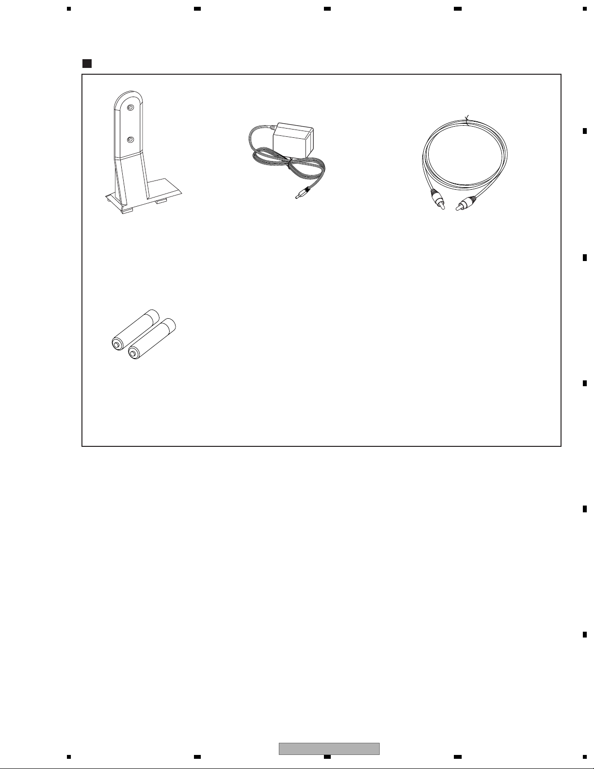
Accessories
Vertical Stand
(WNK2387)
Coaxial digital cable
(WDE1228 / UC)
(WDE1236 / EW)
(WEX1012)
AC/DC Power Adaptor
(WWR1017 / UC)
(WWR1018 / EW)
Operating Instructions
(WRB1055 / UC/EW)
(WRB1056 / EW)
(WRX1003 / UC)
(WRX1004 / EW)
Warranty card
Rechargeable nickel-metal
hydride batteries (2)
5678
A
B
C
D
56
SE-DIR800C
E
F
7
8
5
Page 6
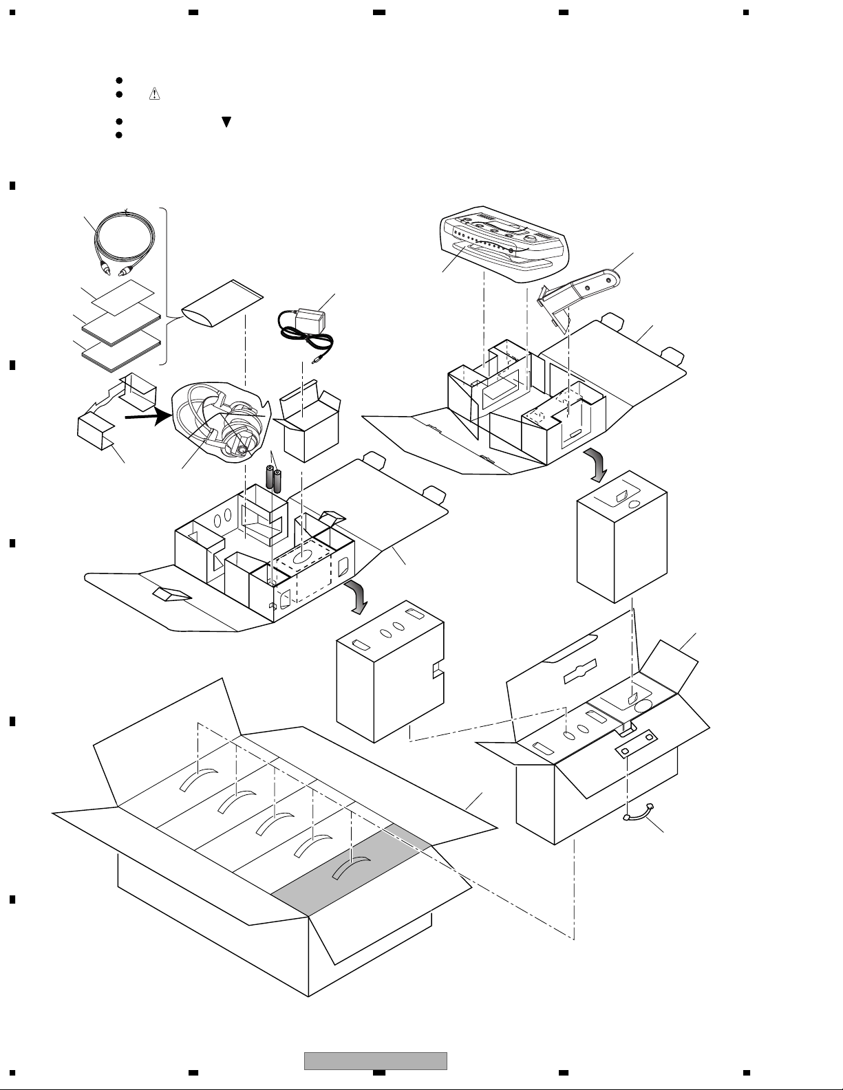
1234
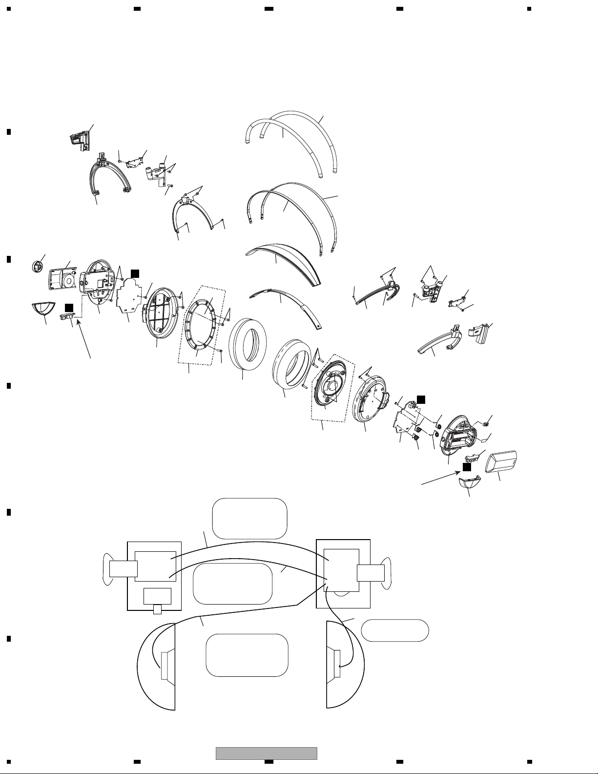
2. EXPLODED VIEWS AND PARTS LIST
NOTES:
A
2.1 PACKING
2
B
C
1
6
6
Parts marked by "NSP" are generally unavailable because they are not in our Master Spare Parts List.
The mark found on some component parts indicates the importance of the safety factor of the part.
Therefore, when replacing, be sure to use parts of identical designation.
Screws adjacent to mark on product are used for disassembly.
For the applying amount of lubricants or glue, follow the instructions in this manual.
(In the case of no amount instructions, apply as you think it appropriate.)
7
4
9
3
13
5
10
9
D
11
E
x5 set
8
12
F
6
1234
SE-DIR800C
Page 7
5678
PACKING Parts List
Mark
Mark
No. Description Part No.
NSP 1 Warranty card See Contrast table(2)
2 Coaxial digital cable See Contrast table(2)
NSP 3 HEADPHONE WPH1021
4 Rechargeble Battery WEX1012
5 Vertical stand WNK2387
6 Operating Instructions See Contrast table(2)
7 AC/DC Power adaptor See Contrast table(2)
>
No. Description Part No.
8 Packing Case See Contrast table(2)
9 Headhone case WHG1864
10 Transmitter case WHG1865
11 Outer carton See Contrast table(2)
12 Handle WNK2160
NSP 13 TRANSMITTER WPX1010
(2) CONTRAST TABLE
SE-DIR800C/KUCXCN1 and SE-DIR800C/NYXCN are constructed the same except for the following :
Mark No. Symbol and Description
NSP
1
Warranty card
2
Coaxial digital cable
Operating Instructions (English, French,
6
Spanish)
Operating Instructions (Garman, Duch,
6
Italian, Portuguese, Swedish)
AC/DC Power adaptor
7
Packing Case
8
Outer carton
11
SE-DIR800C/
KUCXCN1
WRX1003 WRX1004
WDE1228 WDE1236
WRB1055
Not used WRB1056
WWR1017 WWR1018
WHG1946 WHG1947
WHP1603 WHP1610
SE-DIR800C/
NYXCN
WRB1055
A
B
C
D
E
F
56
SE-DIR800C
7
8
7
Page 8
1234
2.2 TRANSMITTER SECTION
A
22
B
11
14
3
C
25
4
7
31
24
5
8
17
29
E
13
16
18
19
10
29
15
28
9
22
33
1
34
32
D
E
F
36
6
12
35
27
2
30
21
21
23
21
21
30
21
26
8
1234
SE-DIR800C
Page 9
5678
TRANSMITTER SECTION Parts List
Mark
Mark
No. Description Part No.
1 PCB Assy WWX1067
2 Weight WNA1127
3 Cover WNK2291
4 Front panel WNK2396
5 Upper case WNK2397
6 Bottom case WNK2422
7 Battery lid WNK2398
8 Upper lens WNK2297
9 Volume knob WNK2393
10 Switching button WNK2394
11 Power button WNK2395
12 Stand WNK2386
13 LED holder_C WNK2302
14 LED holder_L WNK2303
15 LED holder_R WNK2304
16 - terminal WNA1126
17 + terminal WBH1028
18 C terminal WBH1029
No. Description Part No.
19 Connect terminal WBH1030
20 • • • •
21 Foot WEP1061
22 Sheet WER1107
23 Label WRW1067
24 Seal WRW1063
25 Front lens WNK2296
26 Screw PMZ30P060FZK
27 Screw PPZ26P080FZK
28 Screw PPZ30P060FZK
29 Screw PPZ20P050FZK
30 Screw CPZ30P080FNI
NSP 31 Caution sheet See Contrast table(2)
32 Shield sheet WET1020
33 Heat sink WNC1002
34 Screw PMA30P060FZN
35 Screw KPZ14P050FZK
NSP 36 License label See Contrast table(2)
(2) CONTRAST TABLE
SE-DIR800C/KUCXCN1 and SE-DIR800C/NYXCN are constructed the same except for the following :
A
B
C
Mark No. Symbol and Description
31
NSP
NSP
Caution sheet WRN1002 Not used
License label
36
SE-DIR800C/
KUCXCN1
WRW1068 Not used
SE-DIR800C/
NYXCN
D
E
56
SE-DIR800C
F
7
8
9
Page 10
1234
2.3 HEADPHONE SECTION
A
42
43
15
27
35
3
41
18
5
40
42
13
16
40
39
17
40
39
40
A
8
1
Refer to
" 7.1.2 Wiring
processing figure "
26
25
23
24
6
20
36
38
C
11
4
14
40
B
16
21
10
40
D
C
4
7
37
Refer to
" 7.1.2 Wiring
processing figure "
5
19
41
40
42
39
17
B
40
2
40
9
12
44
39
34
42
42
22
27
3
29
28
22
D
Cable wiring Diagram
4 Heart Rittsu wire
L=560
(It lets the inside of a
33
front band tube pass.)
Power
Phot
E
PCB
PCB
SW
1Heart Shield
L=700
(It lets the inside of a
rear band tube pass.)
30
Main
PCB
Vol
Phot
PCB
31
2 Heart Rittsu wire
L=110
R ch
L ch
SP
L
32
2 Heart Rittsu wire
L=700
(It lets the inside of a
front band tube pass.)
SP
R
F
10
SE-DIR800C
1234
Page 11

5678
HEADPHONE SECTION Parts List
Mark
No. Description Part No.
1 Power PCB ASSY WWX1066
2 Main PCB ASSY WWX1065
3 Headband WNA1123
4 Photo cover WNK2282
5 Bracket WNA1125
6 Case L WNK2371
7 Case R WNK2372
8 Base cover L WNK2278
9 Base cover R WNK2279
10 Volume cover WNK2389
11 Battery lid WNK2388
NSP 12 Base R WNK2277
13 Holder_ L WNK2390
14 Holder_ R WNK2391
NSP 15 Base L WNK2276
16 Hanger WNK2375
17 Hanger cover WNK2284
18 Holder cover L WNK2287
19 Holder cover R WNK2399
20 Switch knob WNK2289
A
B
C
21 Volume knov WNK2392
22 Ear pad WNV1113
23 + terminal F WBH1020
24 + terminal R WBH1021
25 - terminal F WBH1022
26 - terminal R WBH1023
27 Band tube WBP1059
28 Rubber band WER1102
29 Band cushion WNV1114
NSP 30 Shield wire WDA1031
NSP 31 Cable WDC1066
NSP 32 Cable WDC1067
NSP 33 Cable WDC1068
NSP 34 Damper WER1103
NSP 35 Resistance WER1104
36 Seal WRW1063
NSP 37 R PHOTO PCB ASSY WWX1069
NSP 38 L PHOTO PCB ASSY WWX1068
39 Screw KPZ14P050FZK
40 Screw PPZ20P060FZK
41 Screw PPZ20P080FZK
42 Screw PPZ25P100FZK
43 L Speaker unit Assy WXX1338
44 R Speaker unit Assy WXX1339
D
E
56
SE-DIR800C
F
7
8
11
Page 12
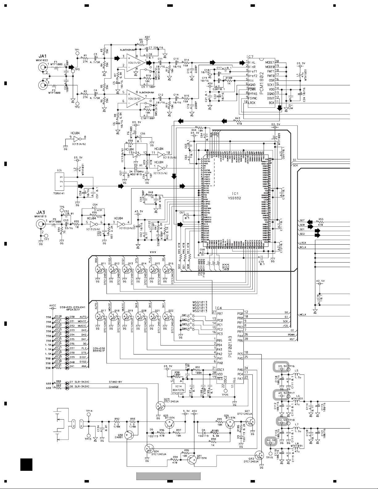
1234
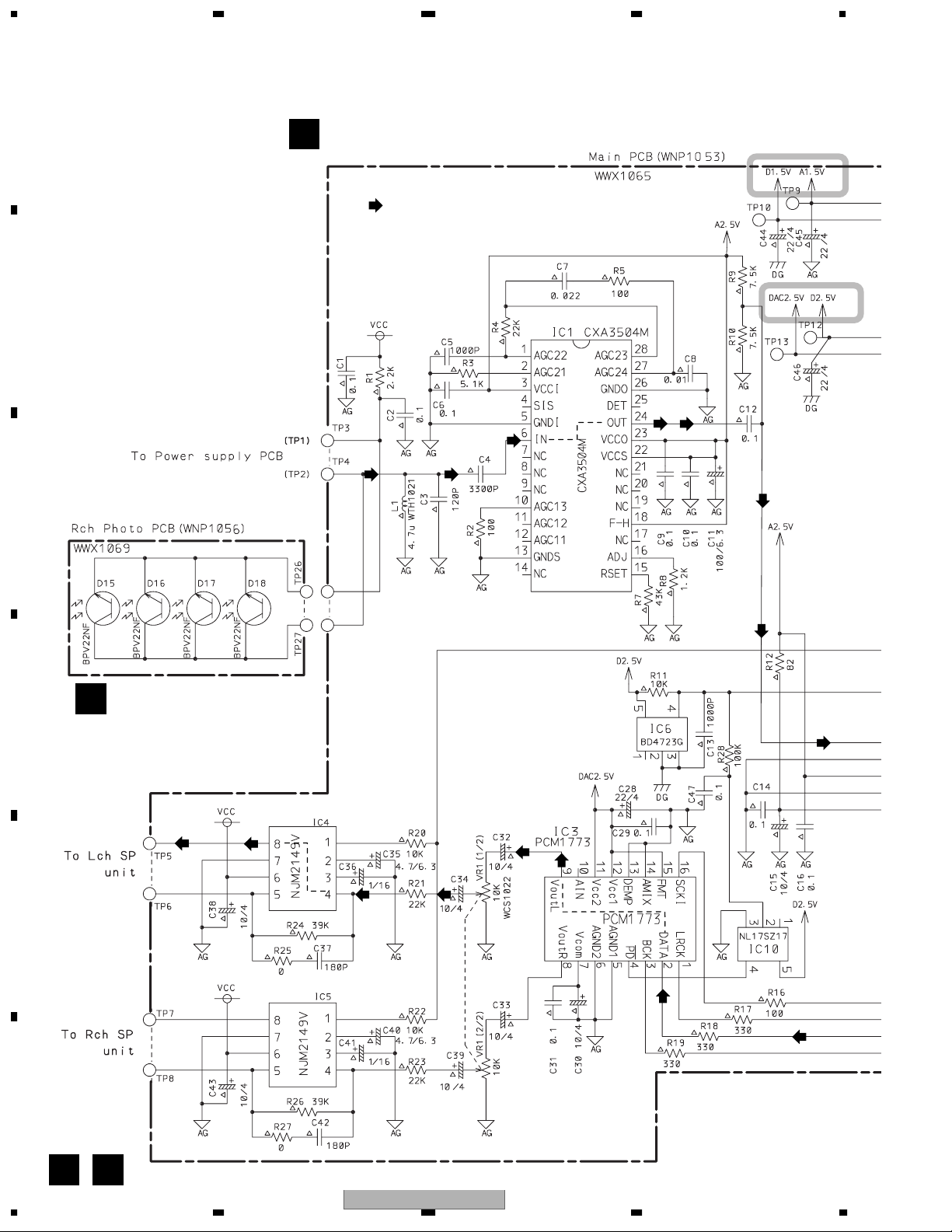
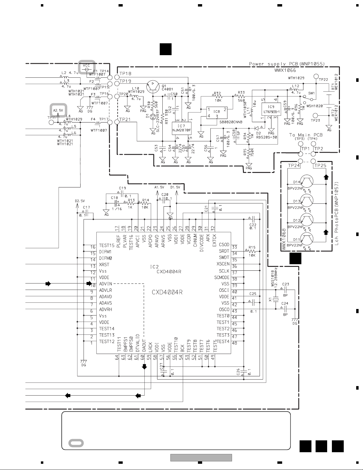
3. BLOCK DIAGRAM AND SCHEMATIC DIAGRAM
3.1 MAIN, POWER, L.PHOTO and R.PHOTO PCB ASSYS
A
MAIN PCB ASSY (WWX1065)
A
: AUDIO SIGNAL ROUTE (L ch)
B
C
R. PHOTO PCB ASSY
D
E
D
(WWX1069)
F
A D
12
1234
SE-DIR800C
Page 13
5678
A
POWER PCB ASSY
B
(WWX1066)
B
L. PHOTO
C
PCB ASSY
(WWX1068)
C
D
E
÷
When ordering service parts, be sure to refer to "EXPLODED VIEWS and PARTS LIST" or
"PCB PARTS LIST".
÷
The > mark found on some component parts indicates the importance of the safety factor
of the part. Therefore, when replacing, be sure to use parts of identical designation.
÷
: The power supply is shown with the marked box.
SE-DIR800C
56
7
F
CA B
13
8
Page 14
1234
3.2 PCB ASSY
A
B
C
D
E
F
E
14
1234
SE-DIR800C
Page 15
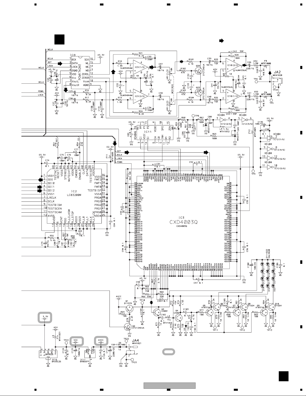
5678
A
PCB ASSY (WWX1067)
E
: AUDIO SIGNAL ROUTE (L ch)
B
C
D
E
: The power supply is shown with the marked box.
SE-DIR800C
56
F
E
7
8
15
Page 16
1234
PCB CONNECTION DIAGRAM
A
B
C
NOTE FOR PCB DIAGRAMS :
1. Part numbers in PCB diagrams match those in the schematic
diagrams.
2. A comparison between the main parts of PCB and schematic
diagrams is shown below.
Symbol In PCB
Diagrams
BCE
BCE
D
Symbol In Schematic
Diagrams
BCEBCE
BCE
DGGSS
BCE
DGS
Part Name
Transistor
Transistor
with resistor
Field effect
transistor
Resistor array
3-terminal
regulator
3. The parts mounted on this PCB include all necessary parts for
several destinations.
For further information for respective destinations, be sure to
check with the schematic diagram.
4. View point of PCB diagrams.
Connector
P.C.Board
Capacitor
Chip Part
SIDE A
SIDE B
4.1 L.PHOTO and R.PHOTO PCB ASSYS
SIDE A SIDE B
D
E
L.PHOTO PCB ASSY
C
(WNP1057)
R.PHOTO PCB ASSY
D
L.PHOTO PCB ASSY
C
To TP2part angle
B
hole Direct solder
R.PHOTO PCB ASSY
D
To TP1part angle
hole Direct solder
B
(WNP1057)
To TP4part angle
A
F
(WNP1056)
hole Direct solder
To TP3part angle
hole Direct solder
C D C D
16
1234
SE-DIR800C
A
(WNP1056)
Page 17
5678
SIDE A SIDE A
SIDE B
SIDE B
B B
POWER
PCB ASSY
POWER
PCB ASSY
B
B
A
TP15
TP19
A
TP17
TP21
A
TP14
TP18
A
TP16
TP20
Q1IC8IC7 IC9
(WNP1055-A)
(WNP1055-A)
A
A
TP4 (Shield Line
Heart Line)
TP2
TP3 (Shield Line
GND)
TP1
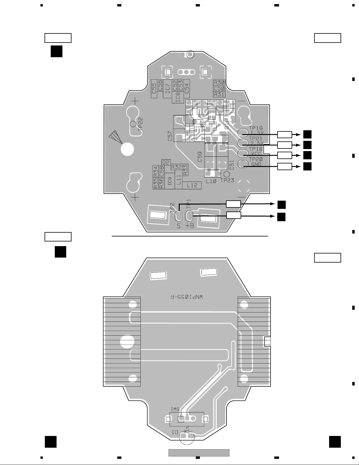
4.2 POWER PCB ASSY
A
B
C
D
56
SE-DIR800C
7
E
F
17
8
Page 18
1234
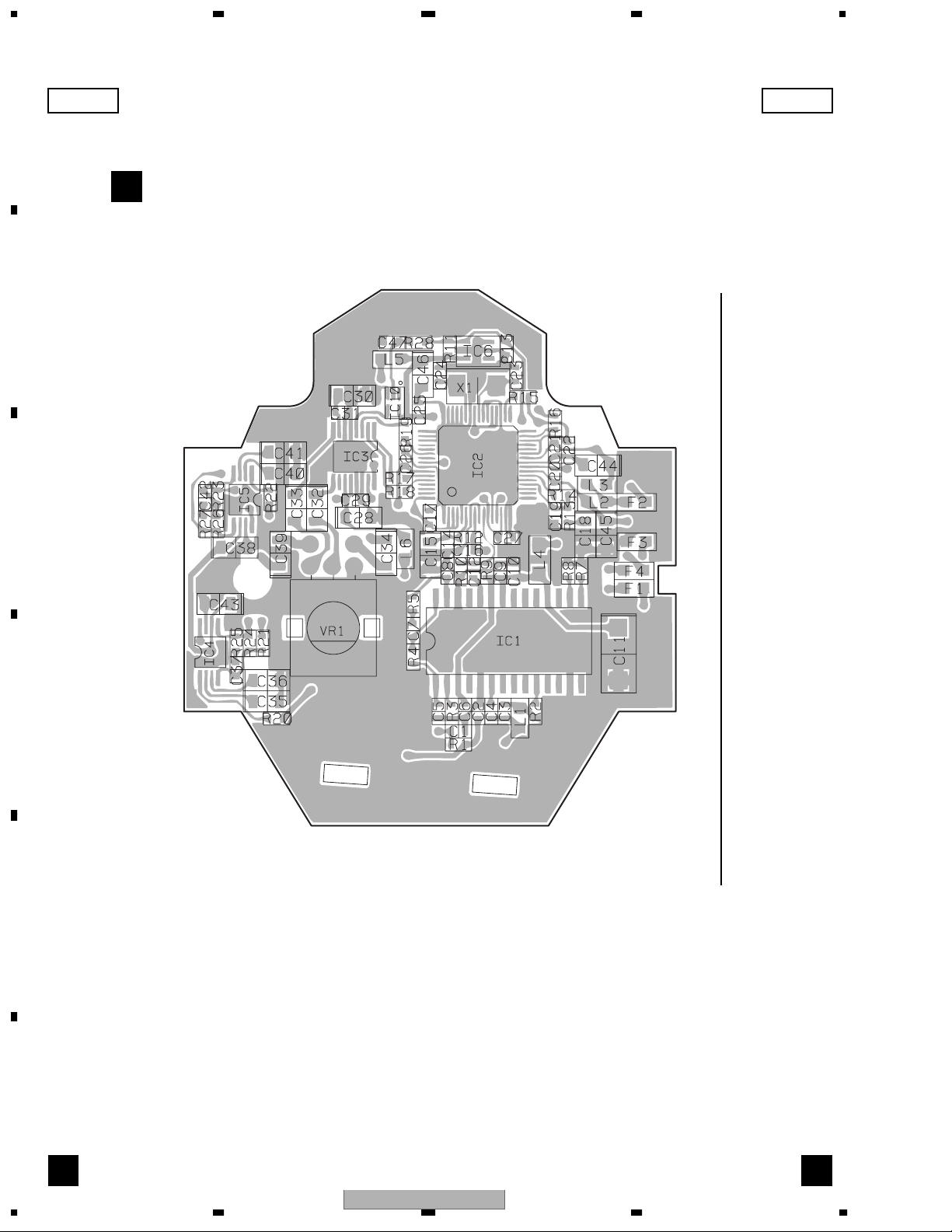
4.3 MAIN PCB ASSY
SIDE A SIDE A
A
B
MAIN PCB ASSY
A
IC6
IC3
IC2
C
VR1
D
E
(WNP1053-A)
IC5
IC1
IC4
F
A A
18
1234
SE-DIR800C
Page 19

5678
SIDE B SIDE B
A A
MAIN PCB ASSY
A
(WNP1053)
B
TP20
TP16
SPEAKER
L ch
TP5
TP6
TP7
SPEAKER
R ch
TP8
B
TP21
TP17
B
TP18
TP14
B
TP19
TP15
TP1
B
B
TP3
TP2
TP4
(Shield Line
Heart Line)
(Shield Line GND)
A
B
C
D
56
SE-DIR800C
7
E
F
19
8
Page 20

1234
4.4 PCB ASSY
A
SIDE A
B
PCB ASSY
E
Q29
Q28
IC16
IC17
IC10
Q11
Q12
IC9
Q13
IC7
IC6
Q19
IC2
IC8
Q17
IC14
Q18
IC4
Q20
Q32
Q27
C
D
E
F
E
20
1234
SE-DIR800C
Page 21

5678
A
SIDE A
Q18
IC4
Q20
Q32
Q27
Q31
Q26
Q5
Q30
IC13
Q21 Q22
IC1
Q14
Q24
Q7
Q1
Q2
Q15
IC5
Q4
IC11
Q16
Q23
IC3
Q3
IC12
Q10
Q9
B
C
E173761
D
E
(WNP1054-A)
F
56
SE-DIR800C
E
7
8
21
Page 22

A
B
SIDE B
1234
PCB ASSY
E
C
D
E
F
E
22
1234
SE-DIR800C
Page 23

5678
A
SIDE B
B
C
D
E
56
SE-DIR800C
7
(WNP1054-A)
F
E
23
8
Page 24

1234
5. PCB PARTS LIST
A
B
NOTES:
Parts marked by "NSP" are generally unavailable because they are not in our Master Spare Parts List.
The mark found on some component parts indicates the importance of the safety factor of the part.
Therefore, when replacing, be sure to use parts of identical designation.
When ordering resistors, first convert resistance values into code form as shown in the following examples.
Ex.1 When there are 2 effective digits (any digit apart from 0), such as 560 ohm and 47k ohm (tolerance is shown by J=5%,
and K=10%).
Ex.2 When there are 3 effective digits (such as in high precision metal film resistors).
560 Ω
47k Ω
0.5 Ω
1 Ω
5.62k Ω
1
56 x 10
47 x 10
R50
1R0
3
561
473
1
5621
LIST OF ASSEMBLIES
Mark
NSP 1..DIGITAL CORDLESS HEADPHONE WPH1021 WPH1021
NSP 1..Composite PCB ASSY WNX1019 WNX1019
NSP 2..L.PHOTO PCB ASSY WWX1068
NSP 2..R.PHOTO PCB ASSY WWX1069 WWX1069
C
NSP 1..TRANSMITTER WPX1010 WPX1010
Symbol and Description
2..MAIN PCB ASSY WWX1065 WWX1065
2..Power PCB ASSY WWX1066 WWX1066
SE-DIR800C
/KUCXCN
SE-DHT800C
/NYXCN
WWX1068
RD1/4PU J
RD1/4PU J
RN2H K
RS1P K
RN1/4PC F562 x 10
561
473
R50
1R0
5621
NSP 1..Gathering PCB ASSY WNX1020 WNX1020
2.. PCB ASSY WWX1067 WWX1067
Mark No. Description Part No.
MAIN PCB ASSY
A
SEMICONDUCTORS
D
IC3 PCM1773PWR
IC1 CXA3504M
IC2 CXD4004R
IC4, IC5 NJM2149V
IC6 BD4723G
IC10 NL17SZ17DFT2G
COILS AND FILTERS
F1, F2, F3, F4 EMI Filter WTF1007
L1, L2, L3, L5, L6 Chip inductor WTH1021
L4 Chip inductor WTH1029
E
CAPACITORS
C3 CCSRCH121J50
C37, C42 CCSRCH181J50
C23, C24 CCSRCH8R0D50
C5, C13 CKSRYB102K50
C8 CKSRYB103K50
C7 CKSRYB223K50
C4 CKSRYB332K50
C1, C12, C10, C14, C16, C17 CKSRYF104Z25
C19, C2, C20, C22, C21, C26 CKSRYF104Z25
F
C25, C27, C29, C31, C6, C9,C47 CKSRYF104Z25
C15, C30, C32, C33, C34, C38 CSZS100M4
C39, C43 CSZS100M4
C18, C36, C41 CSZS1R0M16
24
1234
SE-DIR800C
Mark No. Description Part No.
C28, C44, C45, C46 CSZS220M4
C35, C40 CSZS4R7M6R3
C11 CSZSC101M6R3
RESISTORS
R25, R27 RS1/16S0R0J
R16, R2, R5 RS1/16S101J
R13 RS1/16S102J
R11, R14, R15, R20, R22 RS1/16S103J
R28 RS1/16S104J
R8 RS1/16S122J
R1 RS1/16S222J
R21, R23, R4 RS1/16S223J
R18, R19, R17 RS1/16S331J
R24, R26 RS1/16S393J
R7 RS1/16S433J
R3 RS1/16S512J
R10, R9 RS1/16S752J
R12 RS1/16S820J
VR1 Volume (10k) WCS1022
OTHERS
X1 Ossillator (12.28MHz) WSS1018
POWER PCB ASSY
B
SEMICONDUCT
IC9 LT1615ES5-1
IC7 NJM2870F25
IC8 S-80820CNNB-B8F
ORS
Page 25

5678
Mark
No. Description Part No.
Q1 2SC4081
D1 SLC-22VR3F
D2 RB520S-30
COILS AND FIL
L11 Chip inductor WTH1030
L10, L12 Chip inductor WTH1029
CAP
ACITORS
C58 CCSRCH5R0C50
C50, C52, C53, C56 CKSRYF105Z10
C54, C55 CSZS220M4
C51, C57, C59 CSZSC101M6R3
RESIST
ORS
R32 RS1/16S103J
R34, R36 RS1/16S105J
R31 RS1/16S331J
R30, R33 RS1/16S561J
R35 RS1/16S754J
TERS
SWITCH
SW1 WSH1020
L.PHOTO PCB ASSY
C
SEMICONDUCTORS
L Photo PCB WNP1057
D11, D12, D13, D14 BPV22NF
R.PHOTO PCB ASSY
D
SEMICONDUCTORS
R Photo PCB WNP1056
D15, D16, D17, D18 BPV22NF
PCB ASSY
E
SEMICONDUCTORS
IC17 BA05SFP
IC16 BA33C25FP
IC14 BD4727G
IC3 CXD4003Q
IC2 LC83200W
Mark
No. Description Part No.
D30, D31, D32, D33, D34, D35 MPG4361F
D39, D40, D41 MPG4361F
D36, D37, D38 BR4361F
D11, D12, D13, D14, D15, D16 DAL5820
D17, D18, D19, D20, D21, D22 DAL5820
D7, D8 SLR-342VC
COILS AND FIL
F1, F2, F3,F4, F5 EMI Filter WTF1008
F10, F11, F12, F6, F7,F8,F9 Filter WTF1009
L1, L2, L6, L8, L9 Inductor WTH1031
L3 Chip inductor WTH1032
L4 Chip inductor WTH1026
L5, L7 Inductor LAYU1R5K
CAP
ACITORS
C57, C58, C122 CCSRCH100D50
C1, C10, C2, C75, C77, C88, C89, C9 CCSRCH101J50
C42, C43 CCSRCH390J50
C33, C34 CCSRCH391J50
C54, C55 CCSRCH470J50
C108, C60 CCSRCH471J50
C11, C12, C13, C14, C18 CEAT100M16
C19, C22, C24, C26, C28 CEAT100M16
C29, C30, C37, C38, C39 CEAT100M16
C40, C5, C50, C6, C61 CEAT100M16
C110 CEAT101M16
C112, C115, C116, C118 CEAT101M16
C121, C135 CEAT101M16
C100 CEAT101M25
C125, C44 CEAT102M16
C46, C47, C7 CEAT221M16
C35, C41, C53, C79, C86 CEAT330M16
C3, C4 CEAT4R7M50
C123, C134, C52 CKSRYB103K50
C130, C131 CKSRYB152K50
C15, C16 CKSRYB222K50
C59, C63, C81 CKSRYB472K50
C101, C102, C103, C104, C105 CKSRYF104Z25
C106, C107, C109, C111, C113 CKSRYF104Z25
C114, C117, C119, C120, C124 CKSRYF104Z25
TERS
A
B
C
D
IC11 MC74HC4046AF
IC6, IC9 NJM3404AM
IC10 NJM4556AL
IC8 PCM1742KEG/2K
IC7 PCM1802DBR
IC4 PEF001A9
IC12, IC13 TC74HCU04AF
IC5 TORX141
IC1 YSS932-S
Q5, Q7, Q9 2SA1037AK
Q1, Q25, Q26, Q31 2SB1197K
Q4, Q3, Q30 2SC4081
Q10, Q6, Q8 2SD1664
Q11, Q12, Q13, Q14, Q15, Q16 DTC124EUA
Q17, Q18, Q19, Q2, Q20, Q21 DTC124EUA
Q22, Q23, Q24, Q27, Q28, Q29, Q32 DTC124EUA
D6 1SR139-400
D3, D4, D5, D9 1SS119
D1, D2 MA2Z371
56
C126, C17, C20, C21, C23, C25 CKSRYF104Z25
C27, C36, C45, C51, C56, C62 CKSRYF104Z25
C64, C65, C66, C67, C68, C69 CKSRYF104Z25
C70, C71, C72, C73, C74, C76 CKSRYF104Z25
C78, C8, C80, C82, C83, C84, C85 CKSRYF104Z25
C90, C91, C92, C93, C94, C95, C96 CKSRYF104Z25
C97, C98, C99 CKSRYF104Z25
C132, C133, C32, C87 CKSRYF105Z10
C48, C49 CQMA103K50
C127 (2200uF/25) WCH1011
RESISTORS
R79, R82, R85 RD1/4PS100JL
R92 RD1/4PS1R2JL
R93 RD1/4PS1R5JL
R32, R33 RD1/4PS330JL
R22, R29, R35 RS1/16S100J
R58, R77, R80, R83 RS1/16S101J
R40, R71, R98, R100 RS1/16S102J
R10, R11, R12, R13, R44, R57, R64 RS1/16S103J
SE-DIR800C
E
F
7
8
25
Page 26

1234
Mark
No. Description Part No.
R69, R95, R97, R99 RS1/16S103J
R28, R31, R62, R63, R90, R91 RS1/16S104J
A
B
C
R38 RS1/16S105J
R14, R15, R65, R75 RS1/16S151J
R126, R127, R128, R74 RS1/16S152J
R25, R26, R72 RS1/16S153J
R18, R19 RS1/16S182J
R9 RS1/16S220J
R68 RS1/16S221J
R37, R70, R78, R81, R84 RS1/16S222J
R1, R2 RS1/16S273J
R73 RS1/16S242J
R67 RS1/16S272J
R66 RS1/16S331J
R105 RS1/16S332J
R120, R121, R122, R123, R124 RS1/16S391J
R125, R129, R130, R131 RS1/16S391J
R3, R4, R5, R6 RS1/16S393J
R39, R43, R45, R46, R47 RS1/16S471J
R51, R54, R55, R94, R96 RS1/16S471J
R101, R104, R60, R76 RS1/16S472J
R102, R103, R36 RS1/16S473J
R42 RS1/16S512J
R56 RS1/16S562J
R61, R88, R89 RS1/16S681J
R7, R8 RS1/16S682J
R59 RS1/16S684J
R34 RS1/16S750J
R16, R17, R21, R24, R41, R106 RS1/16S822J
VR1 Volume (10k) WCS1022
SWITCHES AND RELAYS
SW1, SW2, SW3, SW4 WSG1013
SW5 WSH1018
OTHERS
D
E
JA1 JACK (2P) WKN1022
JA2 JACK (HP) WKN1020
JA3 JACK (1P) WKN1019
Heat Sink WNC1002
X1 Oscillator (24.57MHz) WSS1019
JA4 Jack WKN1021
ADJUSTMENT
There is no information to be shown in this chapter.
F
26
1234
SE-DIR800C
Page 27

5678
Symptom: No recharging possible
Insert the dedicated rechargeable battery (supplied) into the battery case
of the transmitter.
Check the periphery of Q25 and
R92-R93 of the transmitter.
START
Does the CHARGE
LED light up?
Short-circuit between
TP14 and TP15.
Does the CHARGE
LED light up for 5 sec.?
Check the periphery of the
charge terminal.
No
No
Ye s
Ye s
Ye s
Check the peripheries of Q24, Q26, Q27,
Q30, Q31, and Q32 of the transmitter.
7. GENERAL INFORMATION
7.1 DIAGNOSIS
7.1.1 TROUBLE SHOOTING
A
B
C
D
E
F
56
SE-DIR800C
7
8
27
Page 28

1234
Symptom: No sound from the cordless headphones
A
Connect the AC adaptor while holding the POWER
START
B
switch and the ProLogic II switch of the transmitter pressed.
(Noise simulation mode)
Is sound output from
the headphone terminal
No
of the transmitter?
Ye s
C
Is the IR-LED-drive
waveform normal?
No
(TP11-TP13)
D
Ye s
Check the headphones.
E
F
28
SE-DIR800C
1234
Check the transmitter.
Page 29

5678
Symptoms: Failure in sound and indication of the transmitter (Checking the transmitter)
Connect the AC adaptor while holding the POWER switch
and the INPUT switch of the transmitter pressed.
Check the power source (AVCC).
Check the peripheries of the LED
drive TR and of microcomputer (IC4).
Check the peripheries of the following:
headphone output (IC10), filter (IC9),
DSP (IC2), DECODER (IC1), and
D/A (IC8).
Check the peripheries of IC11 and IC12.
Check the peripheries of IC3,
and of the IR-LED-drive TR.
START
Did all the LEDs light up
in order?
Disconnect the AC adaptor.
Connect the AC adaptor while holding the POWER
switch and the ProLogic II switch of the transmitter
pressed.
Is noise output from
the headphone terminal?
Is the VCOT circuit
oscillating? (TP9)
Is the IR-LED-drive waveform
normal? (TP11-TP13)
POWER-OFF
Yes
Yes
Yes
Yes
No
No
No
No
A
B
C
D
E
SE-DIR800C
56
7
8
F
29
Page 30

1234
A
Connect a player (DIGITAL 1, DIGITAL 2, and analog).
POWER ON
B
Is sound output?
No
Check the peripheries of
IC5 and IC1.
Switch to DIGITAL 2.
C
Is sound output?
No
Check the peripheries
Ye s
of IC13 and JA3.
Switch to analog input.
D
No
Is sound output?
Check the peripheries of A/D
(IC7), IC6 and JA1.
Ye s
E
After three minutes or more
of continuous playback,
No
Checking audio detection
Check the peripheries of IC9 and Q1.
does the IR LED
remain lit?
Ye s
OK
F
30
1234
SE-DIR800C
Page 31

5678
Symptoms: Failure in sound and indication of the cordless headphones (Checking the headphones)
START
Insert the battery and set the Power switch to ON.
Does the LED light up?
Is each voltage
(VCC, A1.5 V, D1.5 V,
A2.5 V, D2.5 V, and
DAC2.5 V) OK?
Is sound output while
signals are being received?
OK
Check the Power Board Assy,
lead wires, and the peripheries
of Q1 and D1.
Check the Power Board Assy,
the peripheries of IC7, IC8,
and IC9, and the periphery of Q1.
Check the Photo Board Assy, and the
peripheries of the following:
IC1 (RF amplifier), IC2 (decoder),
IC3 (DAC), IC4 and IC5 (power amplifier),
and the speaker.
Ye s
No
No
No
Ye s
Ye s
A
B
C
D
E
F
56
SE-DIR800C
7
8
31
Page 32

1234
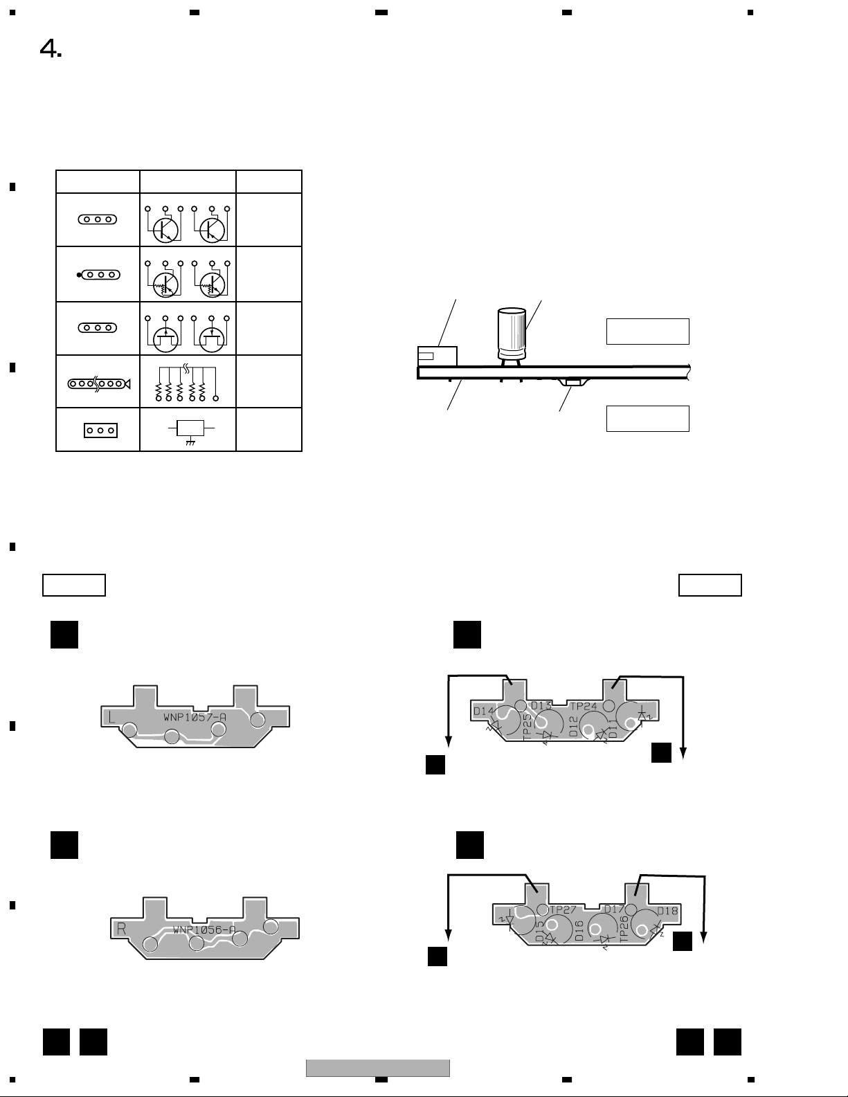
7.1.2 Disassembly
7 Transmitter
A
1. Remove the two screws of the stand.
2. Remove the four screws of the lower case.
3. Slide the cover of the upper and lower cases.
4. Remove the lower case.
5. Remove the soldering from the charge terminal.
6. Remove the three fixing screws of the phono jack.
7. Remove the Board Assy from the upper case with the VR control attached.
B
Board Assy
7 Headphones
<L side>
C
1. Remove the ear pad.
2. Remove the three screws of the base and remove the base.
3. Remove the two screws of the base cover and remove the base cover.
4. Remove the soldering from the lead wire on the photo board.
5. Remove the screw of the board.
POWER BOARD Assy
6. Remove the photo cover.
D
PHOTO BOARD Assy
<R side>
1. Remove the ear pad.
2. Remove the three screws of the base and remove the base.
3. Remove the two screws of the base cover and remove the base cover.
4. Remove the soldering from the lead wire on the photo board.
5. Remove the screw of the board.
E
6. Remove the photo cover.
MAIN BOARD Assy
PHOTO BOARD Assy
F
32
1234
SE-DIR800C
Page 33

5678
Wire dressing
Wire dressing
Wire dressing
Shielding wire
Shielding wire
7 Lead dressing on the L-ch side
Incorrect dressing of the wire may result
in insufficient transmissible distance
between the transmitter and the cordless
headphones.
7 Lead dressing on the R-ch side
Incorrect dressing of the wire may result
in insufficient transmissible distance
between the transmitter and the cordless
headphones.
A
B
C
D
E
SE-DIR800C
56
7
F
33
8
Page 34

1234
7.2 IC
• The information shown in the list is basic information and may not correspond exactly to that shown in the schematic diagrams.
A
B
List of IC
YSS932, LC83200W, CXD4003Q, PEF001A9, CXA3504M, CXD4004R
TRANSMITTER TRE-D800
YSS932 (PCB ASSY : IC1)
• 96kHz DIR + Dolby Digital / Pro Logic II / DTS Decoder + SubDSP
Pin Arrangement (Top view)
VSS
SCK
/ICSOSI
128
127
125
126
124
TESTXI
TESTXO
VDD2
TESTMS
C
D
E
TESTXEN
IPORT0
IPORT1
IPORT2
IPORT3
IPORT4
DDIN0
DDIN1
DDIN2
DDIN3
VSS
CPO
AVDD
DIRPCO
DIRPRO
AVSS
TESTBRK
TESTR1
TESTR2
VDD1
SDWCKI0
SDBCKI0
/SDBCKO
SDIA
SDOA2
SDOA1
SDOA0
SDIB3
SDIB2
SDIB1
SDIB0
VSS
XO
XI
1
2
3
4
5
6
7
8
9
10
11
12
13
14
15
16
17
18
19
20
21
22
23
24
25
26
27
28
29
30
31
32
33
34
35
36
37
38
/CS
DIRINT
123
122
/LOCK
121
CRC
SURENC
119
120
VDD1
118
KARAOKE
117
MUTE
116
AC3DATA
115
DTSDATA
114
VSS
NONPCM
ZEROFLG
OVFB/END
113
111
112
110
RAMA17
109
RAMA16
108
RAMA15
107
RAMA14
106
RAMA13
105
RAMA12
104
VDD2
103
102
101
100
99
98
97
96
95
94
93
92
91
90
89
88
87
86
85
84
83
82
81
80
79
78
77
76
75
74
73
72
71
70
69
68
67
66
65
VSS
RAMA11
RAMA10
RAMA9
RAMA3
RAMA4
RAMA2
RAMA5
RAMA1
RAMA6
RAMA0
RAMA7
RAMA8
VDD1
VSS
RASN
RAMOEN
RAMWEN
CASN
RAMD15
RAMD14
RAMD13
RAMD12
RAMD11
RAMD10
RAMD9
RAMD8
VDD1
VSS
RAMD7
RAMD6
RAMD5
RAMD4
RAMD3
RAMD2
RAMD1
RAMD0
VDD2
60
OPORT4
62
64
VSS
OPORT6
OPORT5
OPORT7
56
OPORT0
58
OPORT1
OPORT2
OPORT3
55
53
51
49
44
ERR/BS
SYNC/U
46
FS128/C
DBL/V
43
41
39
VDD2
F
34
1234
42
40
DIRSDO
DIRBCK
DIRWCK
DIRMCK
47
45
50
48
VSS
SDOB3
SDBCKI1
SDWCKI1
SE-DIR800C
54
52
SDOB2
SDOB0
SDOB1
VDD1
59
57
63
61
Page 35

Block Diagram
DIRMCK
DDIN0
DDIN1
DDIN2
DDIN3
DDINSEL
V
ERR/BS
DBL/V
DIRINT
PLL DIR
DIRO Interface
DIRBCK
DIRWCK
SDIASEL
SDIA Interface
SDIACKSEL
SDWCKI0
SDBCKI0
/SDBCKO
CRC
DIRPCO
DIRSDO
SDIA
SURENC
KARAOKE
MUTE
CRC
AC3DATA
DTSDATA
NONPCM
ZEROFLG
XI
XO
CPO
PLL
Clock for DIR
Block (25MHz)
Clock for DSP
Block (30MHz)
SDOA Interface
MainDSP
(AC-3/ProLogicII/DTS decoder)
SDIB Interface
SDOA0
SDOA1
SDOA2
L,R
LS,RS
C,LFE
SDIB0
SDIB1
SDIB2
SDIB3
SDIBSEL
SDIBCKSEL
External Memory
Interface
SubDSP
RAMD0-15
CASN
RASN
RAMWEN
RAMOEN
RAMA0-17
OVFB/END
SDOB Interface
SDOBCKSEL
SDOB3
SDOB2
SDOB1
SDOB0
SDWCKI1
SDBCKI1
OPORT0-7
Coefficient /
Program RAM
MPLOAD
/CS
SO
SI
SCK
IPORT0-4
Control Signal
DBL
Control Register
Microprocessor I/F
VMOD BSMOD
ERR
BS
SYNC
U
FS128
C
SYNC/U
FS128/C
UMOD CMOD
OVFSEL
OVFB
END
7 6 5 IPORT5-7
DIRPRO
/LOCK
5678
A
B
C
D
56
SE-DIR800C
E
F
7
8
35
Page 36

1234
Pin Function
No. Pin Name I/O Function
A
B
C
D
E
1 TESTXI I LSI Test pin (must be connected to VSS)
2 TESTXO O LSI Test pin (to be open)
3 VDD2
4 XO O Crystal oscillator connection
5 XI I Crystal oscillator connection (24.576MHz)
6 TESTMS I+ LSI Test pin (to be open)
7 TESTXEN I+ LSI Test pin (to be open)
8 IPORT0 I+ General purpose input port
9 IPORT1 I+ General purpose input port
10 IPORT2 I+ General purpose input port
11 IPORT3 I+ General purpose input port
12 IPORT4 I+ General purpose input port
13 DDIN0 Is DIR: Digital audio interface data input 0
14 DDIN1 Is DIR: Digital audio interface data input 1 / General purpose input port
15 DDIN2 Is DIR: Digital audio interface data input 2 / General purpose input port
16 DDIN3 Is DIR: Digital audio interface data input 3 / General purpose input port
17 VSS
18 CPO A PLL filter connection
19 AVDD
20 DIRPCO A DIR: PLL filter connection
21 DIRPRO A DIR: PLL filter connection
22 AVSS
23 TESTBRK I+ LSI Test pin (to be open)
24 TESTR1 I+ Initial Clear input for PLL in DSP block
25 TESTR2 I+ LSI Test pin (to be open)
26 VDD1
27 SDWCKI0 I+ Word clock input for SDIA, SDOA, SDIB, SDOB
28 SDBCKI0 I+ Bit clock input for SDIA, SDOA, SDIB, SDOB
29 /SDBCKO O Reverse clock output of DIRBCK or SDBCKI0
30 SDIA I Input of bitstream or PCM data to Main DSP
31 SDOA2 O PCM data output from Main DSP (C, LFE)
32 SDOA1 O PCM data output from Main DSP (LS, RS)
33 SDOA0 O PCM data output from Main DSP (L, R)
34 SDIB3 I+ PCM data input 3 to Sub DSP
35 SDIB2 I+ PCM data input 2 to Sub DSP
36 SDIB1 I+ PCM data input 1 to Sub DSP
37 SDIB0 I+ PCM data input 0 to Sub DSP
38 VSS
39 VDD2
40 DIRSDO O Output of bitstream or PCM data from DIR
41 DIRWCK O DIR: Serial data word clock (fs) output
42 DIRBCK O DIR: Serial data bit clock (64fs) output
43 DIRMCK O DIR: Serial data master clock (256fs or 128fs) output
44 ERR/BS O DIR: Data error detect / Block start output
45 SYNC/U O DIR: Serial data synchronized timing / User data output
46 FS128/C O DIR: Serial data master clock 128fs / Channel status output
47 DBL/V O DIR: Double rate lock detect / Validity flag output
48 SDWCKI1 I+ Word clock input for SDIB, SDOB
49 SDBCKI1 I+ Bit clock input for SDIB, SDOB
50 VSS
−
+2.5V power supply (for internal core logic)
−
Ground
−
+3.3V power supply (for DIR block)
−
Ground (for DIR block)
−
+3.3V power supply (for I/O)
−
Ground
−
+2.5V power supply (for internal core logic)
−
Ground
F
36
1234
SE-DIR800C
Page 37

5678
No. Pin Name I/O Function
51 SDOB3 O PCM data output from Sub DSP
52 SDOB2 O PCM data output from Sub DSP
53 SDOB1 O PCM data output from Sub DSP
54 SDOB0 O PCM data output from Sub DSP
55 VDD1
−
+3.3v power supply (for I/O)
56 OPORT0 O General purpose output port (LED control : DD)
57 OPORT1 O General purpose output port (LED control : PL2)
58 OPORT2 O General purpose output port (LED control : DTS)
59 OPORT3 O General purpose output port (LED control : DIG1)
60 OPORT4 O General purpose output port (LED control : DIG2)
61 OPORT5 O General purpose output port (LED control : ANA)
62 OPORT6 O General purpose output port
63 OPORT7 O General purpose output port
64 VSS
−
Ground
65 VDD2
−
+2.5V power supply (for internal core logic)
66 RAMD0 I+/O Sub DSP: External memory interface Data 0
67 RAMD1 I+/O Sub DSP: External memory interface Data 1
68 RAMD2 I+/O Sub DSP: External memory interface Data 2
69 RAMD3 I+/O Sub DSP: External memory interface Data 3
70 RAMD4 I+/O Sub DSP: External memory interface Data 4
71 RAMD5 I+/O Sub DSP: External memory interface Data 5
72 RAMD6 I+/O Sub DSP: External memory interface Data 6
73 RAMD7 I+/O Sub DSP: External memory interface Data 7
74 VSS
−
Ground
75 VDD1
−
+3.3V power supply (for I/O)
76 RAMD8 I+/O Sub DSP: External memory interface Data 8
77 RAMD9 I+/O Sub DSP: External memory interface Data 9
78 RAMD10 I+/O Sub DSP: External memory interface Data 10
79 RAMD11 I+/O Sub DSP: External memory interface Data 11
80 RAMD12 I+/O Sub DSP: External memory interface Data 12
81 RAMD13 I+/O Sub DSP: External memory interface Data 13
82 RAMD14 I+/O Sub DSP: External memory interface Data 14
83 RAMD15 I+/O Sub DSP: External memory interface Data 15
84 CASN O Sub DSP: External DRAM interface Column address strobe output
85 RAMWEN O Sub DSP: External memory interface Write enable output
86 RAMOEN O Sub DSP: External memory interface Output enable output
87 RASN O Sub DSP: External DRAM interface Row address strobe output
88 VSS
−
Ground
89 VDD1
−
+3.3V power supply (for I/O)
90 RAMA8 O Sub DSP: External memory interface Address 8
91 RAMA7 O Sub DSP: External memory interface Address 7
92 RAMA0 O Sub DSP: External memory interface Address 0
93 RAMA6 O Sub DSP: External memory interface Address 6
94 RAMA1 O Sub DSP: External memory interface Address 1
95 RAMA5 O Sub DSP: External memory interface Address 5
96 RAMA2 O Sub DSP: External memory interface Address 2
97 RAMA4 O Sub DSP: External memory interface Address 4
98 RAMA3 O Sub DSP: External memory interface Address 3
99 RAMA9 O Sub DSP: External memory interface Address 9
100 RAMA10 O Sub DSP: External memory interface Address 10
A
B
C
D
E
F
56
SE-DIR800C
7
8
37
Page 38

1234
No. Pin Name I/O Function
101 RAMA11 O Sub DSP: External memory interface Address 11
A
102 VSS
103 VDD2
104 RAMA12 O Sub DSP: External memory interface Address 12
105 RAMA13 O Sub DSP: External memory interface Address 13
106 RAMA14 O Sub DSP: External memory interface Address 14
107 RAMA15 O Sub DSP: External memory interface Address 15
108 RAMA16 O Sub DSP: External memory interface Address 16
109 RAMA17 O Sub DSP: External memory interface Address 17
110 OVFB/END O Sub DSP: Overflow / Program end detect
111 ZEROFLG O Main DSP: Zero flag output
B
112 VSS
113 NONPCM O Main DSP: non-PCM data detect
114 DTSDATA O Main DSP: DTS data detect
115 AC3DATA O Main DSP: AC-3 data detect
116 MUTE O Main DSP: Auto mute detect
117 KARAOKE O Main DSP: AC-3 Karaoke data detect
118 VDD1
119 SURENC O Main DSP: AC-3 2/0 mode Dolby Surround Encode input detect
120 CRC O Main DSP: AC-3 CRC error detect
121 /LOCK O DIR: PLL lock detect
C
122 DIRINT O DIR: interrupt output
123 /CS Is Microprocessor interface Chip select input
124 SO Ot Microprocessor interface Data output
125 SI Is Microprocessor interface Data input
126 SCK Is Microprocessor interface Clock input
127 /IC Is Initial clear input
128 VSS
I : Input pin
Is : Schmitt trigger input pin
I+ : Input pin with a pull-up resistor
D
O : Output pin
Ot : Tri-state output pin
A : Analog pin
−
Ground
−
+2.5V power supply (for internal core logic)
−
Ground
−
+3.3V power supply (for I/O)
−
Ground
E
F
38
1234
SE-DIR800C
Page 39

5678
LC83200W (PCB ASSY : IC2)
• Dolby Headphone LSI
Pin Arrangement (Top view)
A
B
C
D
E
SE-DIR800C
56
F
7
8
39
Page 40

1234
Block Diagram
A
Data RAM
B
11.5k×24bits
Program ROM
15kW×32bits
Input RegisterOutput Register
C
Status I/O I/F
Control Register
Host I/F
D
E
F
40
1234
SE-DIR800C
Page 41

5678
Pin Function
Block No. Pin Name I/O Function
Audio IN
7 LRCLOCK I LR clock for audio data input
8 SCLOCK I Bit clock for audio data input
3 SDI0 I Audio data serial input (L, R)
4 SDI1 I Audio data serial input (Ls, Rs)
5 SDI2 I Audio data serial input (C, LFE)
Audio OUT 2 SDO O Audio data serial output (L, R)
Host I/F
41 ENABLE I Command enable input
40 CLOCK I Serial data input clock
39 DATA I Address and data input
Reset 47 RESET I System reset input (Low: reset on)
PLL
14 R I VCO bias resistor pin
15 VCNT I VCO control input pin
23 MCLOCK I Moving clock input pin
16 PDO O Output pin for VCO charge pump
Power
supply
1,19 VDD1 − I/O power supply
25,37,43 VDD2 − Digital power supply
13 AVDD − Power supply for PLL
6,20 VSS1 − I/O GND
31,36,46 VSS2 − Digital GND
12 AVSS − GND for PLL
Test
9,10,11,17,24 I Test pin
32,38 O Test pin
Parallel
control
port
42 CMODE I Parallel (High) / Serial (Low) selection pin
30 PRG4 I
Dolby headphone mode selection pin
29 PRG3 I
28 PRG2 I
27 PRG1 I
26 PRG0 I
35 FMT2 I
Audio I/O selection pin
34 FMT1 I
33 FMT0 I
44 MUTE I Mute pin (High: Mute on)
45 STEREO I Bypass setting pin of LR signal (High: Stereo bypass)
18 PLL STOP I Power save pin (Low: PLL circuit OFF)
21 PLL1 I
PLL clock selection pin
22 PLL0 I
A
B
C
D
E
56
SE-DIR800C
F
7
8
41
Page 42

1234
CXD4003Q (PCB ASSY : IC3)
• Digital signal-processing LSI that provides functions for both transmission and reception
A
B
in the DIAT (Digital Infrared Audio Transmission) system
Pin Arrangement (Top view)
C
D
E
F
42
1234
SE-DIR800C
Page 43

Block Diagram
5678
A
B
C
D
E
56
SE-DIR800C
F
7
8
43
Page 44

1234
Pin Function
No. Pin Name I/O Function
A
B
C
D
E
1 VSS − Digital GND
2NC − Non connection
3NC
4 DAAVD − Analog power supply for RF DAC
5 DAAOUT O RF DAC output
6 DAAVS − Analog GND for RF DAC
7 DAVRO I/O Internal current setting for RF DAC
8 DAVREF I Reference voltage input for RF DAC
9NC − Non connection
10 ADAVS − Analog GND for RF ADC
11 ADVRH I Reference voltage input for RF DAC (high)
12 ADAVD − Analog power supply for RF DAC
13 ADVRL I Reference voltage input for RF DAC (low)
14 ADVIN I RF ADC input
15 TEST1 I Test pin, normally fixed to L
16 TEST2 I Test pin, normally fixed to L
17 VSS
18 TEST3 I Test pin, normally fixed to L
19 TEST4
20 TEST5 I Test pin, normally fixed to L
21 TEST6 I Test pin, normally fixed to L
22 TEST7
23 TEST8 I/O Test pin, normally open-circuit
24 TEST9 I/O Test pin, normally open-circuit
25 TEST10 I/O Test pin, normally open-circuit
26 TEST11
27 TEST12 I/O Test pin, normally open-circuit
28 VSS − Digital GND
29 TEST13 I/O Test pin, normally open-circuit
30 TEST14 I/O Test pin, normally open-circuit
31 TEST15 I/O Test pin, normally open-circuit
32 TEST16 I Test pin, normally fixed to L
33 VDD − Digital power supply
34 TEST17 O Test pin, normally open-circuit
35 TEST18 O Test pin, normally open-circuit
36 TEST19 O Test pin, normally open-circuit
37 TEST20 O Test pin, normally open-circuit
38 TEST21
39 VSS
40 TEST22 I Test pin, normally fixed to L
41 TEST23 I Test pin, normally fixed to L
42 TEST24 I Test pin, normally fixed to L
43 TEST25 I Test pin, normally fixed to L
44 TEST26 I Test pin, normally fixed to L
45 TEST27 I Test pin, normally fixed to L
46 TEST28 I Test pin, normally fixed to L
47 TEST29 O Test pin, normally open-circuit
48 TEST30 O Test pin, normally open-circuit
49 TEST31 O Test pin, normally open-circuit
50 VSS
−
Non connection
−
Digital GND
O
Test pin, normally open-circuit
I
Test pin, normally fixed to L
I/O
Test pin, normally open-circuit
I
Test pin, normally fixed to L
−
Digital GND
−
Digital GND
F
44
1234
SE-DIR800C
Page 45

5678
No. Pin Name I/O Function
51 TEST32 O Test pin, normally open-circuit
52 TEST33 O Test pin, normally open-circuit
53 TEST34
O
Test pin, normally open-circuit
54 TEST35 O Test pin, normally open-circuit
55 TEST36 O Test pin, normally open-circuit
56 VDD − Digital power supply
57 TEST37 I Test pin, normally fixed to L
58 TEST38 O Test pin, normally open-circuit
59 TEST39 O Test pin, normally open-circuit
60 TEST40 O Test pin, normally open-circuit
61 VSS − Digital GND
62 TEST41 O Test pin, normally open-circuit
63 TEST42 O Test pin, normally open-circuit
64 TEST43 O Test pin, normally open-circuit
65 TEST44 I Test pin, normally fixed to L
66 TEST45 I Test pin, normally fixed to L
67 TEST46
I
Test pin, normally fixed to L
68 TEST47 I Test pin, normally fixed to L
69 VSS
−
Digital GND
70 NC − Non connection
71 OSCO O X'tal resonator circuit output (24.576MHz)
72 VSS
−
Digital GND
73 OSCI I X'tal resonator circuit input (24.576MHz)
74 XOSCEN I Stop function control of X'tal resonator circuit
75 TEST48 I Test pin, normally fixed to L
76 TEST49
I
Test pin, normally fixed to L
77 VDD − Digital power supply
78 NC − Non connection
79 VSS − Digital GND
80 TEST50 O Test pin, normally open-circuit
81 TEST51 O Test pin, normally open-circuit
82 TEST52 O Test pin, normally open-circuit
83 VSS − Digital GND
84 TEST53 O Test pin, normally open-circuit
85 TEST54 O Test pin, normally open-circuit
86 TEST55 O Test pin, normally open-circuit
87 VPD I Penetration current prevention pin, normally fixed to L
88 EMP
O
Emphasis output (Off/On=L/H)
89 FSO0
O
Sampling frequency detecting output 0
(FSO1, FSO0) = 00 (44.1kHz), 01 (48kHz),
11 (32kHz)
90 FSO1 O Sampling frequency detecting output 1
91 DTVALID O Data valid flag (Valid/Invalidity = H/L)
92 TXOUT O Digital audio interface format output
93 DAOUT O Data output for audio DA converter
94 VSS − Digital GND
95 RXIN I Digital audio interface format input
96 DTIN I Data input
97 BCKIN I Bit clock input
98 LRCKIN I LR clock input (L ch/R ch = H/L)
99 LRCKO O LR clock output (L ch/R ch = H/L)
100 VDD
−
Digital power supply
56
SE-DIR800C
A
B
C
D
E
F
7
8
45
Page 46

1234
No. Pin Name I/O Function
A
B
C
D
E
101 BCKO O Bit clock output
102 DACLKO O Clock output for audio DA converter, 256fs (VCOR/2)
103 DTOK
104 C12 O 12.288MHz clock output (OSCI/2)
105 VSS − Digital GND
106 TEST56 I/O Test pin, normally open-circuit
107 TEST57 I/O Test pin, normally open-circuit
108 TEST58 O Test pin, normally open-circuit
109 TEST59 I/O Test pin, normally open-circuit
110 PDDN O Phase comparison output down
111 PDUP O Phase comparison output up
112 PLVAR O PLL comparator output (VCOT/640 or VCOR/512)
113 PLREF O PLL reference output (fs)
114 TEST60 I Test pin, normally fixed to L
115 TEST61 I Test pin, normally fixed to L
116 VSS − Digital GND
117 VCOR
118 TEST62 I Test pin, normally fixed to H
119 TEST63
120 VCOT I Transmission VCO input
121 VDD − Digital power supply
122 TEST64
123 TEST65 I Test pin, normally fixed to L
124 TEST66 I Test pin, normally fixed to L
125 TEST67 I Test pin, normally fixed to L
126 TEST68
127 VSS − Digital GND
128 CSOD O Chapter start delay output
129 CSO O Chapter start output
130 SCMODE I Serial control mode selection (Pin/Serial = L/H)
131 TRMODE I Transmission/Reception mode selection (Transmission/Reception = L/H)
132 TEST69 I Test pin, normally fixed to L
133 DIVCODE I Full/Half band mode selection (Full/Half = L/H)
134 CHNUM I Channel number selection (0 ch/1 ch = L/H)
135 TEST70 I Test pin, normally fixed to L
136 ERRO O Error output (No error/Error = L/H)
137 TEST71 O Test pin, normally open-circuit
138 VSS
139 XRST
140 XRSTS I Software reset (Reset=L)
141 IIFSEL0 I Input selection 0
142 TEST72 I Test pin, normally fixed to L
143 MLSEL I MSB/LSB selection of digital-audio AD/DA converter data
144 VDD − Digital power supply
145 PSSEL I Front/back squeeze selection of digital-audio AD/DA converter data
146 XMUTE I Mute input (Mute/Through = L/H)
147 CRCCK I CRC check request (Off/On = L/H)
148 TEST73 I Test pin, normally fixed to L
149 VSS − Digital GND
150 SRDT
O
Receive data condition (Good/poor = H/L)
I
Reception VCO input
I
Test pin, normally fixed to H
I
Test pin, normally fixed to L
I
Test pin, normally fixed to H
−
Digital GND
I
Hardware reset (Reset=L)
O
Read-out output of CPU interface data
F
46
1234
SE-DIR800C
Page 47

5678
No. Pin Name I/O Function
151 SCLK I Clock input of CPU interface data
152 XLAT I Latch input of CPU interface data
153 SWDT
I
Writing input of CPU interface data
154 TEST74 O Test pin, normally open-circuit
155 TEST75 I Test pin, normally fixed to L
156 TEST76 O Test pin, normally open-circuit
157 TEST77 O Test pin, normally open-circuit
158 TEST78 O Test pin, normally open-circuit
159 TEST79 O Test pin, normally open-circuit
160 VSS − Digital GND
161 TEST80 O Test pin, normally open-circuit
162 TEST81 O Test pin, normally open-circuit
163 TEST82 O Test pin, normally open-circuit
164 TEST83 O Test pin, normally open-circuit
165 VDD − Digital power supply
166 TEST84 O Test pin, normally open-circuit
167 TEST85
I
Test pin, normally fixed to L
168 TEST86 I Test pin, normally fixed to L
169 TEST87
O
Test pin, normally open-circuit
170 TEST88 O Test pin, normally open-circuit
171 VSS − Digital GND
172 TEST89
O
Test pin, normally open-circuit
173 TEST90 O Test pin, normally open-circuit
174 TEST91 O Test pin, normally open-circuit
175 TEST92 I Test pin, normally fixed to L
176 TEST93
O
Test pin, normally open-circuit
A
B
C
D
56
SE-DIR800C
E
F
7
8
47
Page 48

1234
PEF001A9 (PCB ASSY : IC4)
• 8-bit 1-chip microcomputer
A
Pin Arrangement (Top view)
1
PB5
2
PB4
3
PA3
4
PA2
5
PA1
6
PA0
7
PB3
8
B
PB2
PB1/BZ
PB0/BZ
VSS
PG0/INT
PC0/TMR0
PC1
9
10
11
12
13
14
28
PB6
27
PB7
26
PA4
25
PA5
24
PA6
23
PA7
22
OSC2/PG2
21
OSC1/PG1
20
VDD
19
RES
18
PC5/TMR1
17
PC4
16
PC3
15
PC2
Pin Function
Pin Name
No.
C
D
E
1 PB5 O LED control
2 PB4 O LED control
3 PA3 O LED control
4 PA2 O LED control
5 PA1 O LED control
6 PA0 O LED control
7 PB3 O Chip enable output for DSP
8 PB2 O Chip select output for DSP
9 PB1 O Serial clock output
10 PB0 O Serial data output
11 VSS − Ground
12 PG0 I Serial data input
13 PC0 I Key input 1
14 PC1 I Key input 2
15 PC2 I Key input 3
16 PC3 I Key input 4
17 PC4 I Battery detection input
18 PC5 I Battery voltage abnormality detection
19 RES − External reset input
20 VDD − Power supply
21 OSC1 I CR oscillation input
22 OSC2 O Oscillation output
23 PA7 O LED control
24 PA6 O Charge control
25 PA5 O IR LED control
26 PA4 O A/D reset output
27 PB7 O DSP reset output 1
28 PB6 O DSP reset output 2
I/O Pin Function
F
48
1234
SE-DIR800C
Page 49

5678
CXA3504M (MAIN PCB ASSY : IC1)
• DIAT Receiver Analog Signal Processing IC
Block Diagram
HEADPHONE SE-DHP800
A
B
C
D
E
SE-DIR800C
56
F
7
8
49
Page 50

1234
Pin Function
Pin Name
No.
A
B
1 AGC22 O AGC response setting pin
2 AGC21 O Charging current control pin
3 VCCI − Power supply of the input section
4 SIS I Electric shunt input pin
5 GNDI − GND of the input section
6 IN I Photodiode input signal pin
7NC − Non connection
8NC − Non connection
9NC − Non connection
10 AGC13 I AGC amplifier input pin
11 AGC12 O Input AGC response setting pin
12 AGC11 O Charging current control pin
13 GNDS − GND of the signal processing section
14 NC − Non connection
15 RSET O Resistor connection pin for power supply setting
16 ADJ O Resistor connection pin for power supply setting for filter Adjust the center frequency of the BPF.
17 NC − Non connection
18 F_H I Filter switching pin Switch the H/L, BPF, Full BPF. H/L BPF: 3 to 4.5MHz, Full BPF: 3 to 6MHz
I/O Pin Function
F_H (pin 18) Mode
L FULL (3 to 6MHz)
C
19 NC − Non connection
20 NC − Non connection
21 NC − Non connection
22 VCCS − Power supply for signal processing section
23 VCCO − Power supply for output section
24 OUT O Signal output pin
25 DET O Output pin for input level detection
26 GNDO − GND for output section
D
E
27 AGC24 O AGC amplifier output pin
28 AGC23 I AGC amplifier input pin
H H/L (3 to 4.5MHz)
F
50
1234
SE-DIR800C
Page 51

5678
CX4004R (MAIN PCB ASSY : IC2)
• Digital Signal-processing IC for DIAT system reception
Pin Arrangement (Top view)
Block Diagram
* Without TEST pin
A
B
C
D
E
56
SE-DIR800C
F
7
8
51
Page 52

1234
Pin Function
No. Pin Name I/O Function No. Pin Name I/O Function
A
B
C
D
E
1 TEST12 I Test pin, normally fixed to L 33 CSOD O Chapter start delayed output
2 TEST13 I Test pin, normally fixed to H 34 SRDT O Read-out output of serial interface data
3 TEST14 I Test pin, normally fixed to H 35 SWDT I Writing input of serial interface data
4 VDDE
5 VSS
6 ADVRH I
7 ADAVS
8 ADAVD
9 ADVRL I
10 ADVIN I RF A/D converter input 42 VSS
11 VDDE
12 VSS
13 XRST I Reset (negative logic) 45 TEST1 I Test pin, normally fixed to L
14 DIFM0 I Select the audio output type 46 TEST2 I Test pin, normally fixed to L
15 DIFM1 I Select the audio output type 47 TEST3 I Test pin, normally fixed to L
16 TEST15 I Test pin, normally fixed to L 48 TEST4 I Test pin, normally fixed to L
17 PLREF O PLL reference output (fs) 49 TEST5 I Test pin, normally fixed to L
18 PLVAR O
19 TEST16 I Test pin, normally fixed to L 51 TEST7 I Test pin, normally fixed to L
20 APVCI I PLL VCO control voltage input 52 TEST8 O Test pin, normally open-circuit
21 VSS
22 APCPO O PLL charge pump 54 BCK O Bit clock output
23 APAVD
24 APAVS
25 VSS
26 VDDI
27 VDDE
28 VCOR I Clock input for data output 60 DAOUT O Data output for audio D/A converter
29 CHNUM I Channel number selection (L: 0ch,H: 1ch) 61 DTVALID O
30 DIVCODE I
31 APX 0 PLL VCO output 63 EMPFS1 O Emphasis, fs information output
32 EXTCK I
−
Digital I/O power supply 36 XSCEN I
−
Digital GND 37 SCLK I Clock input of serial interface data
Reference voltage input for RF A/D
converter (high)
−
Analog GND for RF A/D converter 39 VSS
−
Analog power supply for RF A/D converter 40 OSCI I Crystal resonator circuit input (12.288MHz)
Reference voltage input for RF A/D
converter (low)
−
Digital I/O power supply 43 OSCO O
−
Digital GND 44 TEST0 I Test pin, normally fixed to L
PLL dividing output (256 dividing of APX
output or VCOR input)
−
Digital GND 53 TEST9 O Test pin, normally open-circuit
−
Power supply for PLL VCO 55 TEST10 O Test pin, normally open-circuit
−
GND for PLL VCO 56 VDDE
−
Digital GND 57 VSS
−
Digital internal power supply 58 VDDI
−
Digital I/O power supply 59 LRCK O Audio sampling clock output
Full/Half band mode selection
(L: Full-band, H: Half-band)
Clock selection for data output
(L: APX internal connection, H: VCOR pin
input)
38 SCMODE I
41 VDDE
50 TEST6 I Test pin, normally fixed to L
62 EMPFS0 O Emphasis, fs information output
64 TEST11 I Test pin, normally fixed to H
Enable input of serial interface data
(negative logic)
Control mode selection (L: Pin setting, H:
Serial setting)
−
Digital GND
−
Digital I/O power supply
−
Digital GND
Crystal resonator circuit output
(12.288MHz)
−
Digital I/O power supply
−
Digital GND
−
Digital internal power supply
Data valid flag output
(DTVALID, L: valid, H: Invalidity)
F
52
1234
SE-DIR800C
Page 53

5678
7 Lot mark is sealing indication to the above part of the product.
Indication of lot is four columns
0424
2004
Indicates the total weeks through the year
Date codeTX
RX
Date code location
XXXX
TX sticker
placed in middle
7.3 ABOUT LOT MARK INDICATION
A
B
C
D
56
SE-DIR800C
7
8
E
F
53
Page 54

1234
8. PANEL FACILITIES
A
Controls and displays
Transmitter (top)
B
C
1 STANDBY/ON button
D
E
Press to turn the transmitter on / off.
2 Standby indicator
Lights when the transmitter is in standby.
The indicator is unlit when the transmitter is
on.
3 CHARGE indicator
Lights when the rechargeable batteries are
being charged. The indicator is unlit when
the batteries are fully charged.
4 DOLBY HEADPHONE button
Press to select the Dolby Headphone mode
(DH1 / DH2 / DH3 / OFF).
5 DOLBY PRO LOGIC II button
Press to select the Dolby Pro Logic II mode
(AUTO / MOVIE / MUSIC / OFF).
6 INPUT button
Press to select the source input (DIGITAL 1 /
DIGITAL 2 / ANALOG).
7 VOLUME control
Use to adjust volume level of headphones
(sold separately) connected to the PHONES
jack on the front panel.
8 Battery compartment
Use to recharge the supplied rechargeable
batteries.
F
54
1234
SE-DIR800C
Page 55

5678
Transmitter (front)
1 Infrared transmitters
Infrared transmitters are located on either
side of the unit. Make sure there is an
unobstructed path from the transmitter to
your listening position.
2 DECODE indicators
Light to indicate the automatic decoding
mode for the current source:
2D: Dolby Digital
2PL II: Dolby Pro Logic II decoding of
analog or digital source.
DTS: DTS
3 DOLBY HEADPHONE mode indicators
Light to show the Dolby Headphone mode
(DH1 / DH2 / DH3).
4 DOLBY PRO LOGIC II mode indicators
Light to show the Dolby Pro Logic II mode
(AUTO / MOVIE / MUSIC).
5 INPUT mode indicators
The corresponding indicator lights up to
show the selected input mode (DIGITAL 1 /
DIGITAL 2 / ANALOG).
6 PHONES jack
Use for connecting corded headphones.
A
B
C
D
E
56
SE-DIR800C
F
7
8
55
Page 56

1234
A
Transmitter (rear)
B
C
1 DC IN jack
Connect the supplied AC power adaptor to
this jack. (Use only the supplied AC power
adaptor. Using adpators with different plug
4 DIGITAL IN 2 COAX
Coaxial digital input for connection to digital
audio/video equipment such as a DVD
player, LD player or CD player.
polarities or other characteristics could
cause malfunction.)
D
2 ATT switch
Switches the analog input level between -8dB
and 0dB for compatibility with a wide range
of analog equipment.
5 DIGITAL IN 1 OPT
Optical digital input for connection to digital
audio/video equipment such as a DVD
player, LD player or CD player.
3 LINE IN jacks
Analog input jacks for connection to
audio/video equipment such as a VCR or TV.
E
F
56
1234
SE-DIR800C
Page 57

1 VOL (Volume) control
Use to adjust the volume.
2 Self-adjusting headband
The headband automatically adjusts when
you put the headphones on.
3 POWER indicator
Lights when the headphones are on.
4 POWER switch
Press to turn on / off.
5 Battery compartment
Press and slide where indicated to open the
cover. Use with the supplied rechargeable
batteries or size AA dry-cell batteries.
6 Infrared sensor
Infrared sensors are located on either side.
7 Ear pads
HEADPHONES
5678
A
B
C
D
E
56
SE-DIR800C
F
7
8
57
 Loading...