

Pioneer RSP-99 Service manual
ORDER NO.
PIONEER CORPORATION 1-1, Shin-ogura, Saiwai-ku, Kawasaki-shi, Kanagawa 212-0031, Japan
PIONEER ELECTRONICS (USA) INC. P.O. Box 1760, Long Beach, CA 90801-1760, U.S.A.
PIONEER EUROPE NV Haven 1087, Keetberglaan 1, 9120 Melsele, Belgium
PIONEER ELECTRONICS ASIACENTRE PTE. LTD. 253 Alexandra Road, #04-01, Singapore 159936
PIONEER CORPORATION 2010
CRT4559
RS-P99/EW5
OPTICAL DIGITAL REFERENCE SYSTEM UNIVERSAL DIGITAL PREAMP
RS-P99
/EW5
For details, refer to "Important Check Points for Good Servicing".
K-ZZZ. JUNE 2010 Printed in Japan

1234
1234
C
D
F
A
B
E
SAFETY INFORMATION
Where in a manufacturer’s service documentation, for example in circuit diagrams or lists
of components, a symbol is used to indicate that a specific component shall be replaced only
by the component specified in that documentation for safety reasons, the following symbol shall
be used:
This service manual is intended for qualified service technicians; it is not meant for the casual do-it-yourselfer.
Qualified technicians have the necessary test equipment and tools, and have been trained to properly and safely repair
complex products such as those covered by this manual.
Improperly performed repairs can adversely affect the safety and reliability of the product and may void the warranty.
If you are not qualified to perform the repair of this product properly and safely, you should not risk trying to do so
and refer the repair to a qualified service technician.
2
RS-P99/EW5
5 678
56
7
8
C
D
F
A
B
E
[Important Check Points for Good Servicing]
In this manual, procedures that must be performed during repairs are marked with the below symbol.
Please be sure to confirm and follow these procedures.
1. Product safety
Please conform to product regulations (such as safety and radiation regulations), and maintain a safe servicing environment by
following the safety instructions described in this manual.
1 Use specified parts for repair.
Use genuine parts. Be sure to use important parts for safety.
2 Do not perform modifications without proper instructions.
Please follow the specified safety methods when modification(addition/change of parts) is required due to interferences such as
radio/TV interference and foreign noise.
3 Make sure the soldering of repaired locations is properly performed.
When you solder while repairing, please be sure that there are no cold solder and other debris.
Soldering should be finished with the proper quantity. (Refer to the example)
4 Make sure the screws are tightly fastened.
Please be sure that all screws are fastened, and that there are no loose screws.
5 Make sure each connectors are correctly inserted.
Please be sure that all connectors are inserted, and that there are no imperfect insertion.
6 Make sure the wiring cables are set to their original state.
Please replace the wiring and cables to the original state after repairs.
In addition, be sure that there are no pinched wires, etc.
7 Make sure screws and soldering scraps do not remain inside the product.
Please check that neither solder debris nor screws remain inside the product.
8 There should be no semi-broken wires, scratches, melting, etc. on the coating of the power cord.
Damaged power cords may lead to fire accidents, so please be sure that there are no damages.
If you find a damaged power cord, please exchange it with a suitable one.
9 There should be no spark traces or similar marks on the power plug.
When spark traces or similar marks are found on the power supply plug, please check the connection and advise on secure
connections and suitable usage. Please exchange the power cord if necessary.
a Safe environment should be secured during servicing.
When you perform repairs, please pay attention to static electricity, furniture, household articles, etc. in order to prevent injuries.
Please pay attention to your surroundings and repair safely.
2. Adjustments
To keep the original performance of the products, optimum adjustments and confirmation of characteristics within specification.
Adjustments should be performed in accordance with the procedures/instructions described in this manual.
4. Cleaning
For parts that require cleaning, such as optical pickups, tape deck heads, lenses and mirrors used in projection monitors, proper
cleaning should be performed to restore their performances.
3. Lubricants, Glues, and Replacement parts
Use grease and adhesives that are equal to the specified substance.
Make sure the proper amount is applied.
5. Shipping mode and Shipping screws
To protect products from damages or failures during transit, the shipping mode should be set or the shipping screws should be
installed before shipment. Please be sure to follow this method especially if it is specified in this manual.
RS-P99/EW5
3

1234
1234
C
D
F
A
B
E
CONTENTS
SAFETY INFORMATION..................................................................................................................................... 2
1. SERVICE PRECAUTIONS............................................................................................................................... 5
1.1 SERVICE PRECAUTIONS ........................................................................................................................ 5
1.2 NOTES ON SOLDERING .......................................................................................................................... 5
2. SPECIFICATIONS............................................................................................................................................ 6
2.1 SPECIFICATIONS ..................................................................................................................................... 6
2.2 CONNECTION DIAGRAM ......................................................................................................................... 7
3. BASIC ITEMS FOR SERVICE.......................................................................................................................... 9
3.1 CHECK POINTS AFTER SERVICING....................................................................................................... 9
3.2 JIGS LIST .................................................................................................................................................. 9
4. BLOCK DIAGRAM.......................................................................................................................................... 10
5. DIAGNOSIS.................................................................................................................................................... 14
5.1 OPERATIONAL FLOWCHART................................................................................................................ 14
5.2 CONNECTOR FUNCTION DESCRIPTION............................................................................................. 15
6. SERVICE MODE ............................................................................................................................................ 15
7. DISASSEMBLY .............................................................................................................................................. 16
8. EACH SETTING AND ADJUSTMENT ........................................................................................................... 19
9. EXPLODED VIEWS AND PARTS LIST.......................................................................................................... 20
9.1 PACKING ................................................................................................................................................. 20
9.2 EXTERIOR............................................................................................................................................... 22
10. SCHEMATIC DIAGRAM............................................................................................................................... 24
10.1 CONTROL UNIT(1/2)(GUIDE PAGE) .................................................................................................... 24
10.2 CONTROL UNIT(2/2)(GUIDE PAGE) .................................................................................................... 30
10.3 DSP UNIT(1/2)(GUIDE PAGE) .............................................................................................................. 36
10.4 DSP UNIT(2/2)(GUIDE PAGE) .............................................................................................................. 42
11. PCB CONNECTION DIAGRAM.................................................................................................................... 48
11.1 CONTROL UNIT .................................................................................................................................... 48
11.2 DSP UNIT............................................................................................................................................... 52
12. ELECTRICAL PARTS LIST .......................................................................................................................... 56
4
RS-P99/EW5

5 678
56
7
8
C
D
F
A
B
E
1. You should conform to the regulations govering the product (safety, radio and noise, and other regulations),
and should keep the safety during servicing by following the safety instructions described in this manual.
2. Be careful in handling ICs. Some ICs such as MOS type are so fragile that they can be damaged by
electrostatic induction.
3. "When you carry out the diagnosis and the repair in the cover (CNN3484: spacer, CNN3485: sheet) of this
sound master clock part, remove the cover carefully not to damage it and reuse it after the diagnosis and
the repair."
For environmental protection, lead-free solder is used on the printed circuit boards mounted in this unit.
Be sure to use lead-free solder and a soldering iron that can meet specifications for use with lead-free solders for repairs
accompanied by reworking of soldering.
Compared with conventional eutectic solders, lead-free solders have higher melting points, by approximately 40 C.
Therefore, for lead-free soldering, the tip temperature of a soldering iron must be set to around 373 C in general, although
the temperature depends on the heat capacity of the PC board on which reworking is required and the weight of the tip of
the soldering iron.
Compared with eutectic solders, lead-free solders have higher bond strengths but slower wetting times and higher melting
temperatures (hard to melt/easy to harden).
The following lead-free solders are available as service parts:
Parts numbers of lead-free solder:
GYP1006 1.0 in dia.
GYP1007 0.6 in dia.
GYP1008 0.3 in dia.
1. SERVICE PRECAUTIONS
1.1 SERVICE PRECAUTIONS
1.2 NOTES ON SOLDERING
RS-P99/EW5
5
1234
1234
C
D
F
A
B
E
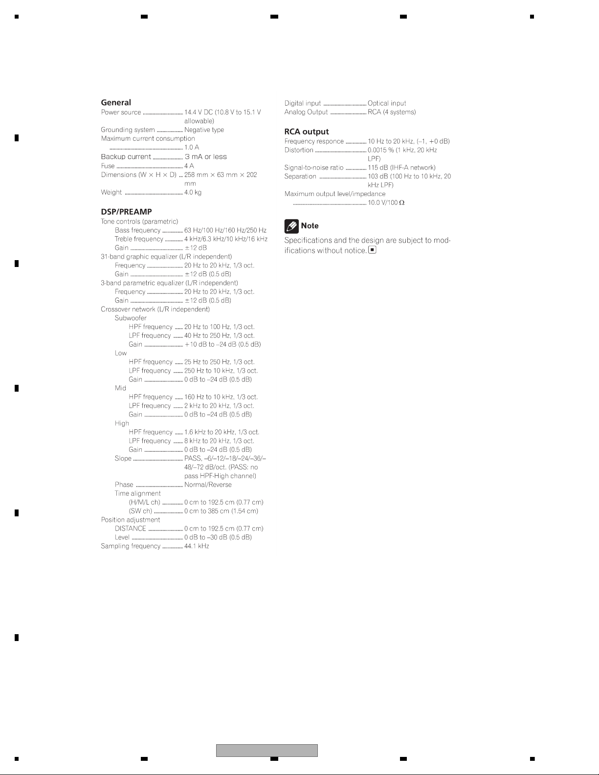
2. SPECIFICATIONS
2.1 SPECIFICATIONS
6
RS-P99/EW5
5 678
56
7
8
C
D
F
A
B
E
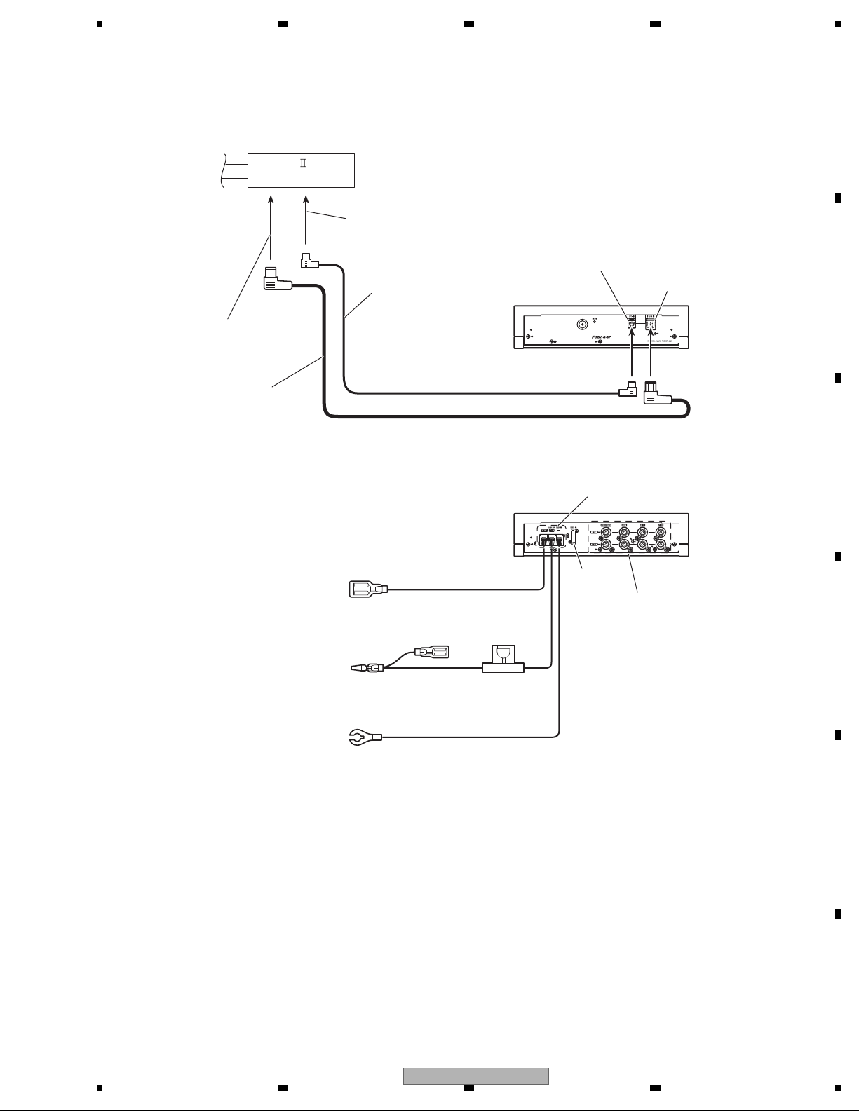
Optical input
(blue)
IP-BUS input
(blue)
IP-BUS cable
(supplied)
optical cable
(supplied)
RS-D7R
(sold separately)
To IP-BUS output
(black)
To optical output
(black)
Fuse (4A)
Right side
Left side
Fuse holder
(4A)
RCA output
Power terminal
Blue/white lead
Connect to system control
terminal of the power amp
(max. 300 mA 12 V DC).
Clear/red lead
Connect to the constant
12 V supply terminal.
Clear/black lead (chassis
ground)
Connect to a clean,
paint-free metal location.
Connection diagram
2.2 CONNECTION DIAGRAM
RS-P99/EW5
7
1234
1234
C
D
F
A
B
E
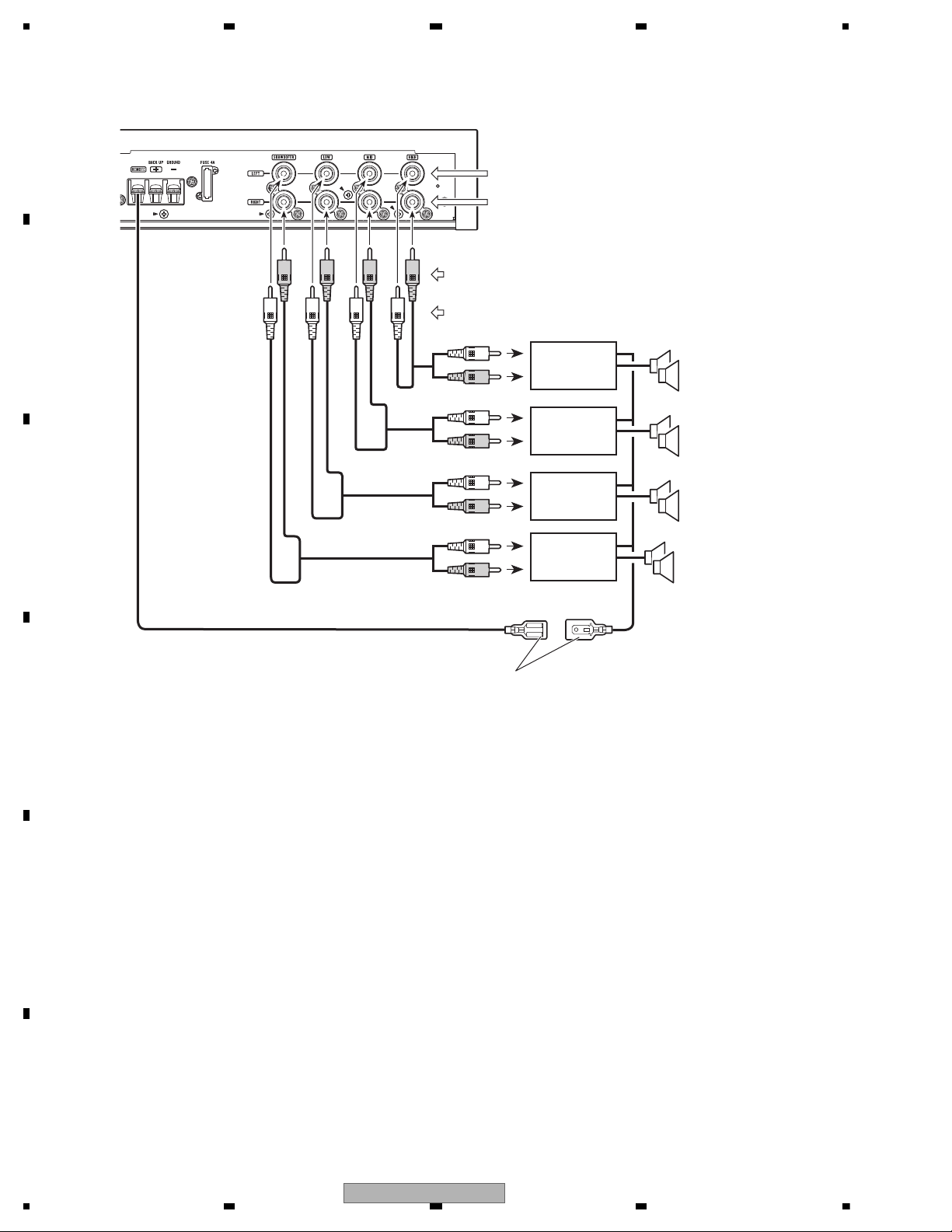
Connecting the RCA input amplifier
White (Left)
Red (Right)
Blue/whiteBlue/white
system remote control
Tweeter
Mid range
Woofer
Subwoofer
Power
amplifier
(sold separately)
Power
amplifier
(sold separately)
Power
amplifier
(sold separately)
Power
amplifier
(sold separately)
White (Left)
Red (Right)
8
RS-P99/EW5
5 678
56
7
8
C
D
F
A
B
E
To keep the product quality after servicing, please confirm following check points.
demrifnoc eb ot metIserudecorP.oN
1 Confirm whether the customer complain has
been solved.
The customer complain must not be
reappeared.
Audio and operations must be normal.
2 Check the output sound. Audio and operations must be normal.
retfa ecnaraeppa sti no trid ro sehctarcs oNkcehc ecnaraeppA3
receiving it for service.
See the table below for the items to be checked regarding audio:
Item to be checked regarding audio
Distortion
Noise
Volume too low
Volume too high
Volume fluctuating
Sound interrupted
DSP Unit
Control Unit
GGD1262
- Jigs List
Name
Extension cable
Jig No.
GGD1262
Remarks
Flexible extension
3. BASIC ITEMS FOR SERVICE
3.1 CHECK POINTS AFTER SERVICING
3.2 JIGS LIST
RS-P99/EW5
9
1234
1234
C
D
F
A
B
E
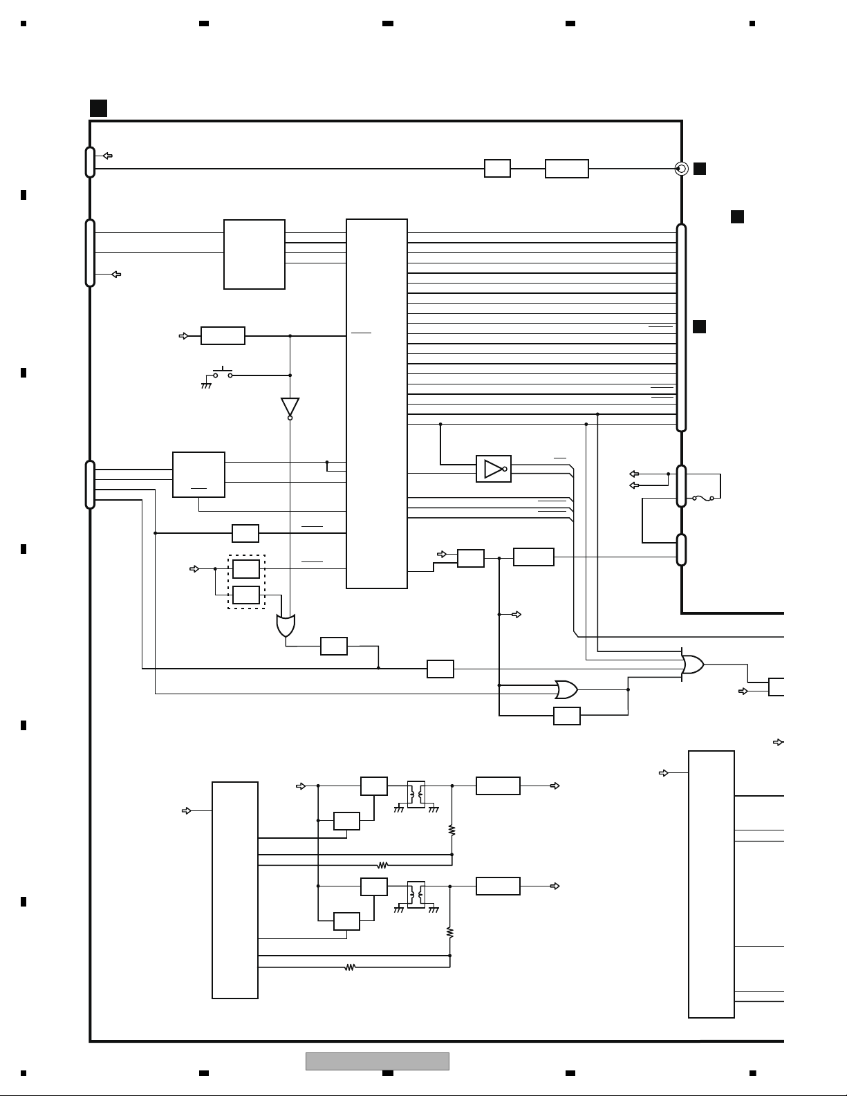
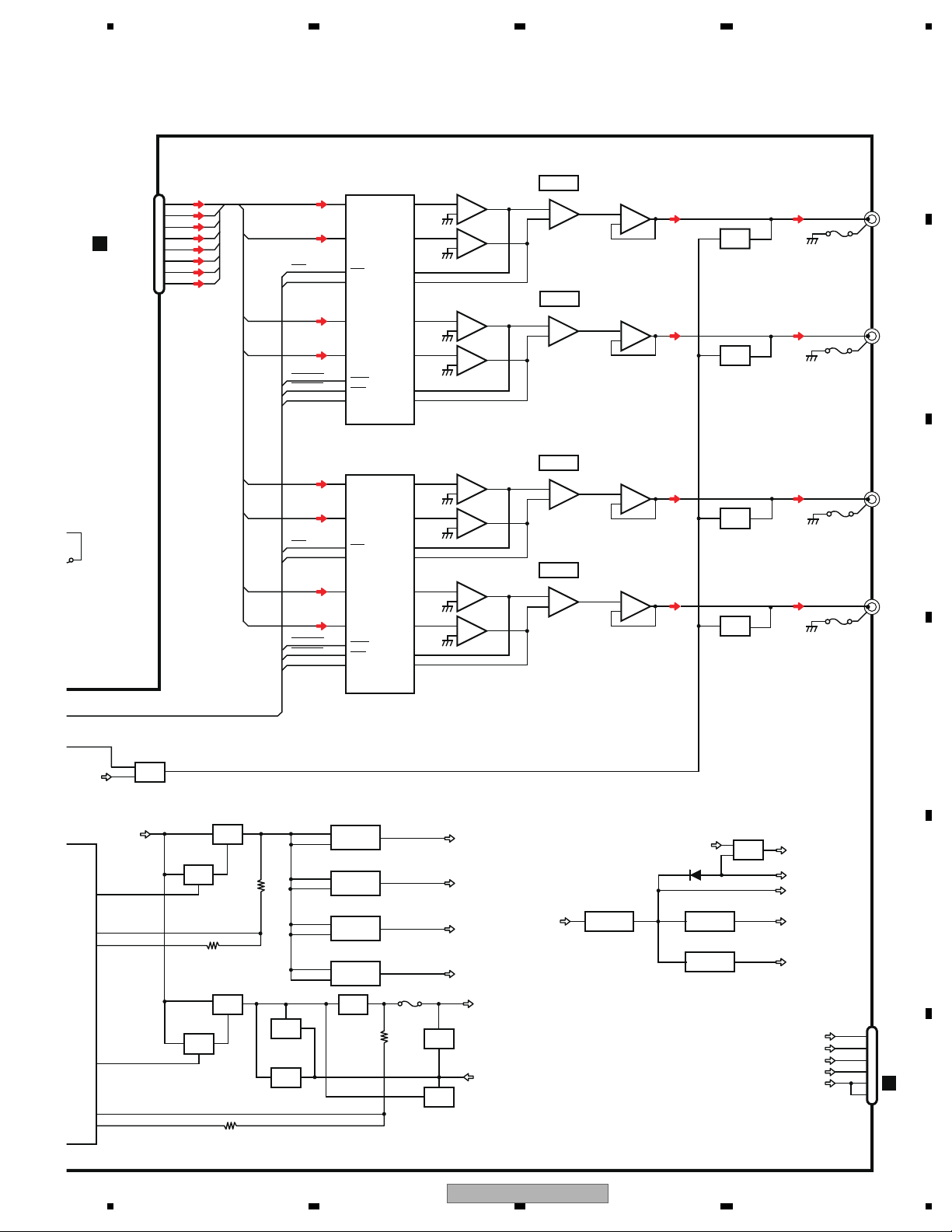
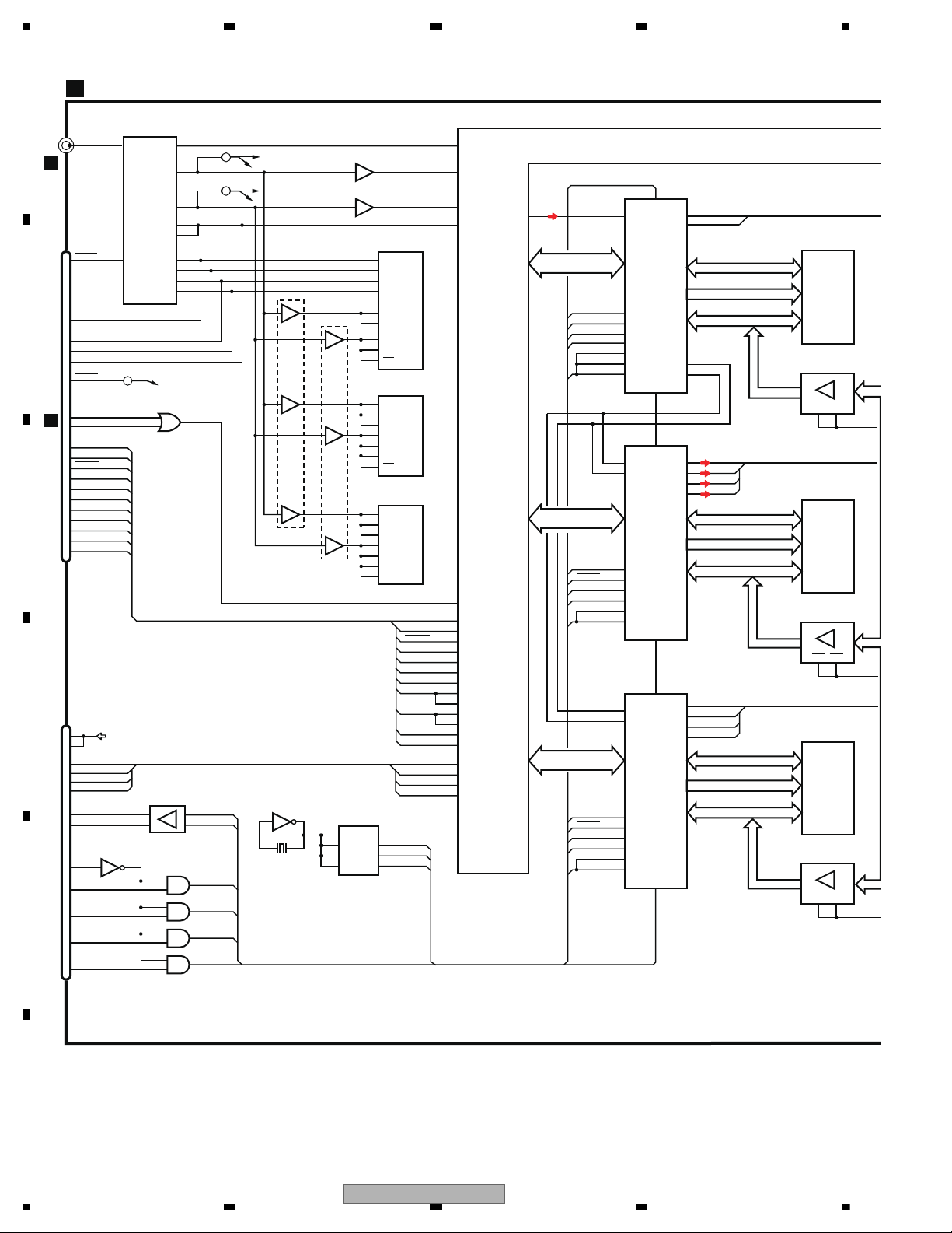
4. BLOCK DIAGRAM
OPT-IN
IP-BUS IN
2
4
5
YA
1
DATA IN
D5V
CONTROL UNIT
TC7WH157FU
1
3
2
D+
2
1
2
1
REM1
B.U
SWBU
BATT
VP15L
±17V REGULATOR
AN8011S
9
OUT2
7
4
IN-2
VCC
T851
OUT1
10
IN+
14
VREF
16
T852
3
OUTIN
1
NJM78M15DL1A
3
OUTIN
2
NJM79M15DL1A
SWBU
3V/6V REGULATOR
AN8011S
9
OUT1
10
13
IN-1
VCC
OUT2
7
4
IN-2
5
8
4
1
BUS+
ASENB
BMUTE
US+5V
USB MICRO
COMPUTER
CY7C68013A-100AXC
18
RXD0
41
40
TXD0
DMINUS
17
DPLUS
37
PB3/FD3
45
PB5/FD5
PEG169A
TC7WH04FU
TXD1
24
25
RXD1
27
P64
6
67
66
1
80
CNVSS
22
P71
23
RX
TX
P70
21IPPW
P76
15
P84
P00
P01
CLK4
Sout4
79
62
61
53
Sin4
P05
P06
P26
43
51
65
63
P40
P30
P02
P04
50
49
46
45
P31
P32
P35
P36
44
47
48
42
1
35
7
5 CLKIN
P37
P34
P33
P41
CLK3
M3.3V
BATT
BATT
SWBU
4
3
5
6
7
8
9
18
20
2
10
12
14
16
22
24
26
28
30
32
DIRRST
DITRST
DIRBRATE1
DIRBRATE0
DIRADFLG
DIREMFLG
DIRUNLOCK
nCONFIG2
nCONFIG1
UMUTE
4 ELDATA
SOUT3
3
P93
2
P94
40
SWBU
ASENM
P43
CONFDONE
PLDRST
DSPERR
DSPSTOP
nSTATUS
PLDIN
PLDOUT
PLDCLK
PLDSEL1
PLDSEL0
EVOLENB
EVOLSTB
ASENS
CLR
4.0A
BATT
VBUM
VBUM
1
OUTIN
6
TPD1018F
19
2
4
OUTVDD
2
POWER ON RESET
S-80827CNUA-B8M
2
ROUT
5
16
P83
BSENS
6
8
1
DIN1
HA12241FP
TC7SET04FUS1
RESET
STBY
RESET
VM15L
BATT
JA301
IC301
CN904
IC851
IC952
IC954
IC801
JA701
IC651
IC601
IC150
IC552
IC621
IC701
IC631
CN302
CN901
H902
CN601
CN5101
CN3001
CN2101
Q541
Q502
Q501
Q511
Q932
Q512
Q311
Q521
Q853
Q851
Q854
Q852
Q52
S401
Q931
B
B
B
Q52
D-
A
BUS-
BUS+
BUS-
OPI1
S/PDIF SELECTOR
SYSTEM MICRO
COMPUTER
IP-BUS DRIVER
18
P81
ACC SENSE
BACK UP SENSE
5
FB2
12
FB1
5
FB2
10
RS-P99/EW5
5 678
56
7
8
C
D
F
A
B
E
1
7
8
4
5
6
2
3
HLP
HLM
MLP
MLM
LLP
LLM
SLP
SLM
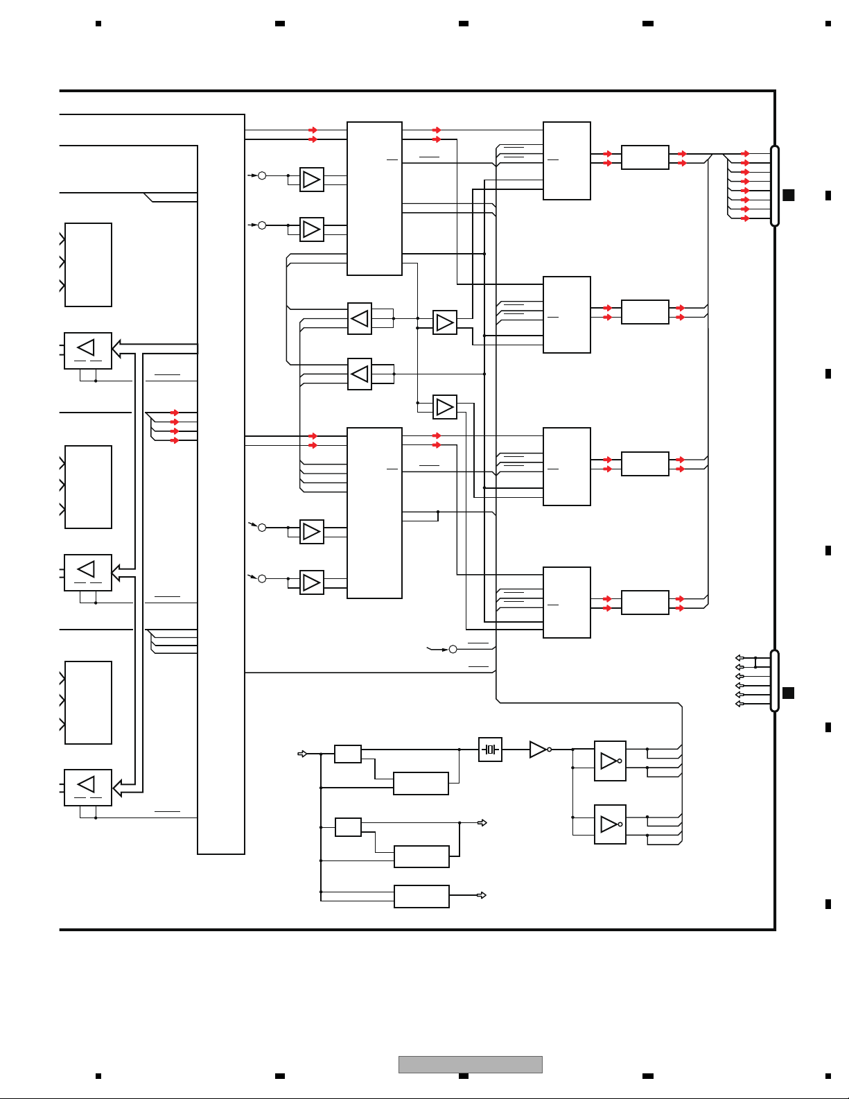
12bit DACx4
AD7564BRS
LT1358CS8
LT1358CS8
LT1358CS8
6
EVOLENB
EVOLSTB
CLR
SDIN
CLKIN
15
16
LDAC
13
FSIN
CLR
12
14
IOUT1C
46
7
8
5
HLP
HLO
MLO
HLM
ELDATA
CLKIN
IOUT1D
13
2
8
5
14
11
RFBC
5
9
RFBD
VREFC
10
VREFD
D3.3V
D5V
DAC5V
VP15L
23MLP
MLM
VREFB
19
VREFA
2
1
3
5
7
6
LT1358CS8
IOUT1B
25 2
1
21
3
IOUT1A
RFBB
24
20
RFBA
6
7
5
3
1
2
12bit DACx4
AD7564BRS
LT1358CS8
6
EVOLENB
EVOLSTB
CLR
SDIN
CLKIN
15
16
LDAC
13
FSIN
CLR
12
14
IOUT1C
46
7
8
5
LLP
LLO
LLM
ELDATA
CLKIN
IOUT1D
RFBC
5
9
RFBD
VREFC
10
VREFD
23SLP
SLM
VREFB
19
VREFA
2
1
3
LT1358CS8
IOUT1B
25 2
1
21
3
IOUT1A
RFBB
24
20
RFBA
6
7
5
SLO
DAC5V
OUT1
10
13
IN-1
OUT2
7
4
IN-2
D5V
4
VOUT
VIN
5
NJM2880U1-05
4
VOUT
VIN
5
NJM2880U1-05
V5DAVOR
4
VOUT
VIN
5
NJM2880U1-05
V5DAVOL
N3.3V
D3.3V
4
VOUT
VIN
5
NJM2880U1-05
N3.3V
VDD5V
VBUM
3
VOUTVIN
2
S-812C33AMC-C2N
M3.3V
3
VOUT
VIN
2
S-812C33AMC-C2N
US3.3V
N3.3V
MUTE
VBUM
Hi-Lch
Mid-Lch
Low-Lch
Sw-Lch
5
7
6
LT1358CS8
(1/2)
(1/2)
3
1
2
LT1358CS8
(2/2)
(2/2)
LT1358CS8
LT1358CS8
5
7
6
3
1
2
5
7
6
LT1358CS8
(1/2)
(1/2)
3
1
2
LT1358CS8
(2/2)
(2/2)
3
VOUTVIN
1
BD3931FP
5V REGULATOR
VM15L
BATT
IC974
IC973
IC972
IC971
IC921
IC931
Q699
IC911
CN101
IC101
IC102
IC104
IC104
CN801
IC103
IC201
IC202
IC203
IC105
IC105
JA102
JA101
IC204
IC204
IC205
IC205
JA202
JA201
P202
P201
CN5101
CN1001
CN3001
CN2101
P102
P801
Q804
Q802
Q813
Q810
Q803
Q811
Q815
Q812
Q523
Q236
Q235
Q136
Q135
B
B
Q522
P101
+
-
+
-
-
+
+
-
+
-
-
+
-
+
-
+
+
-
+
-
-
+
+
-
+
-
-
+
-
+
-
+
Q698
Q814
12
FB1
Q801
5
FB2
CONT
1
CONT
1
CONT
1
CONT
1
PREOUT
BUFFER
BAL→UNBAL
BAL→UNBAL
BAL→UNBAL
BAL→UNBAL
PREOUT
BUFFER
PREOUT
BUFFER
PREOUT
BUFFER
+15VL
-15VL
US+5V
RS-P99/EW5
11
1234
1234
C
D
F
A
B
E
(IAD
0-9
)2,IAD132,ISDA102
(IDAT
0-31
)2
(IDAT
0-7
)2
DATA IN
B
DOUTRXIN
DIR
DIR9001IPWRQ1
Rch EQ DSP
ADSP-21065LCS240S1
TC7WZ34FU
TC7WZ34FU
TC7WZ34FU
TC7SH32FUS1
12
BCKO
11 1 7
BCKO
20
21
4
3
5
6
7
8
9
18
20
2
10
12
14
16
22
24
26
28
30
32
DIRRST
DIRBRATE1
DIRBRATE0
DIRADFLG
DIREMFLG
DIRUNLOCK
nCONFIG2
nCONFIG1
2
nCONFIG
4
1
UMUTE
CONFDONE
PLDRST
DITRST
RST
DSPERR
DSPSTOP
nSTATUS
PLDIN
PLDOUT
PLDCLK
PLDSEL1
PLDSEL0
2
21
23
19
6
8
10
TDI
JTD1
JRST
25
JTCK
27
JTMS
JTEMU
JTD4
31
4
JEMU
JTTD4
JTTRST
JTTD1
JTTCK
JTTMS
TMS
TDO
TCK
JTEMU
JTTD4
JTTRST
JTTMS
JTTCK
UMUTE
CONFDONE
PLDRST
PLDOUT
PLDCLK
DSP UNIT
TC7WZ34FU
LRCKO
10
ERROR
27 DIRUNLOCK
CKSEL
28
EMPH
17 DIREMFLG
FSOUT1
3 DIRBRATE1
FSOUT0
2 DIRBRATE0
AUDIO
1 DIRADFLG
TFS0
7
2
18
RFS0
TFS1
TCLK0
8
4
19
RCLK0
TCLK1
TC74VHC541FK
9
A8
A6
7
6
42
8
11
13
14
12
DSP0CLK
DSP2CLK
DSP1CLK
A5
A7
Y8
Y6
Y5
Y7
IS45S32200E-7TLA1
TC74LCX541FK
146
19 1
TDO
TDI
CLKIN
TMS
149
147
151
23
12
11
22
INSR
INMR
INHR
INLR
TRST
145
TCK
DT1B
TD0B
DT0A
DT1A
PLDDATA
PLD
EPF6016ATI144-3S1
21
PLDBCK
20
PLDLRCK
17
DIRUNLOCK
59
nCONFIG
53
MUTERQ
63
CONF_DONE
105
RESET
89
DSPERR
62
DSPSTOP
60
nSTATUS
56
PLDIN
123
PLDOUT1
124
PLDOUT2
128
PLDCLK1
130
PLDCLK2
125
PLDSEL1
129
PLDSEL0
131
13
TDI
73
TMS
TDO
27
TCK
34
CLK30
92
6
5
17
LRCKO
62
TC7SZU04FU
62
Lch EQ DSP
ADSP-21065LCS240S1
TFS0
7
2
18
RFS0
TFS1
TCLK0
8
4
19
RCLK0
TCLK1
35
35
COEFFICIENT DSP
ADSP-21065LCS240S1
TFS0
7
2
205
RFS0
TCLK0
8
4
RCLK0
76
FLAG11
FLAG8
80
79
78
FLAG9
FLAG10
17
17
30MHz
17
62
JTAG
24
2
1
5
10
13
4
9
12
3
6
8
11
TC7WZ34FU
TC7SH04FUS1
TC74VHC08FK
OE2 OE1
EMU
DR0B
DR0A
(IAD
0-9
)1,IAD131,ISDA101
(IDAT
0-31
)1
(IDAT
0-7
)1
JTEMU
JTTRST
JTTMS
JTTCK
DSP1CLK
IS45S32200E-7TLA1
TC74LCX541FK
30
146
148
TDI
148
19 1
TDO
CLKIN
15
RCLK1
TMS
149
147
151
23
12
11
22
INSL
INML
INHL
INLL
TRST
145
TCK
DT1B
TD0B
DT0A
DT1A
6
5
OE2 OE1
EMU
DR0B
DR0A
(IAD
0-9
)0,IAD130,ISDA100
(IDAT
0-31
)0
(IDAT
0-7
)0
JTEMU
JTTRST
JTTMS
JTTCK
OUTL
JTTD1
DSP0CLK
ADSP-21065
IS45S32200E-7TLA1
TC74LCX541FK
30
146
19 1
TDO
CLKIN
15
RCLK1
19
TCLK1
TMS
149
147
151
23
12
11
22
DS0DT1B
DS0DT1A
TRST
145
TCK
DT1B
TD0B
DT0A
DT1A
OUTL
37 5
OE2 OE1
EMU
DR0A
TDI
148
A
B
C
IRQ0
AA
DSP2CLK
30
15
RCLK1
(1/2)
(1/2)
(1/2)
(2/2)
LCS240S1
CN2101
IC2001
IC2111
IC2101
IC2161
IC3051
CN3001
CN4951
IC2171
IC4901
IC4902
IC4951
IC4953
IC4952
CN601
IC4803
IC4751
IC3001
IC4501
IC4451
IC4201
IC4151
IC4601
IC4301
IC4001
IC4001
Lch EQ DSP
ADSP-21065
(2/2)
LCS240S1
IC4301
Rch EQ DSP
ADSP-21065
(2/2)
LCS240S1
IC4601
X4901
CN302
PLD BCK
PLD LRCK
205
IRQ0
DSP BCK
DSP LRCK
5
7
B33V
JTAG
OSCILLATOR
30MHz CLOCK
DSPCLK/PLDCLK
30MHz
DSP CONTROL
DATA0
COEFFICIENT
DSP
CONTROL DATA
SDRAM
DSP CONTROL
DATA1
CONTROL DATA
SDRAM
SDRAM
CONTROL DATA
205
IRQ0
DSP CONTROL
DATA2
12
RS-P99/EW5
5 678
56
7
8
C
D
F
A
B
E
4
10
9
5
8
7
3
6
HLP
HLM
MLP
MLM
LLP
LLM
SLP
SLM
SDOUTASDINA
SRC0
SRC4184IPAG
DAC-High
I/V CONVERTER
I/V CONVERTER
I/V CONVERTER
I/V CONVERTER
PCM1794ADB
LT1358CS8
TC7WZ34FU
64 558HDATA22
RST
DMUTE
RCKIA
RCKIB
SCK
MUTE
BCKOA
LRCKOA
19 1
DS1BFEN
DMUTE
OE2 OE1
19 1
OE2 OE1
BDAT0-7
TC74LCX541FK
19 1
DS0DT1B
DS0DT1A
OE2 OE1
15
10
8
12
INSL
INML
INHL
109
64
DSP1BFEN
MUTE
INLL
DS2BFEN
16
11
9
14
INSR
INMR
INHR
108
DSP2BFEN
INLR
DS0BFEN
60
53
3
1
5
7
TC7WZ34FU
1
2
7
5
66
67
DSP0DT1B
LRCK2 51
LRCKOB
BCK2
LRCK2
BCK2
LRCK3
BCK3
LRCK4
BCK4
TC7WZ34FU
3
2
5
7
50 62
63 BCK
49
20
29
7
10
S0K5
RST
21
S0K6
SOK4
BCK
6
LRCK
4LRCK5
14
BCKOB
BCKIA
BCKIB
TC7WZ34FU
59
54
3
1
5
7
TC7WZ34FU
3
5
7
TC7WZ34FU
3
5
7
LRCKIA
LRCKIB
DSP0DT1A
110
DSP0BFEN
BCKO
LRCKO
A
B
OUTHLR
SDINB SDOUTB
IOUTL-
26
25
HLP
HLM
IOUTL+
OUT_A
1
7
2
6
OUT_B
55MDATA24
OUTMLR
1
13
7
10
2
4
SDOUTASDINA
SRC1
SRC4184IPAG
TC7WZ34FU
6458LDATA25
RCKIA
RCKIB
60
53
3
1
5
7
LRCK4 62
LRCKOA
LRCK3
51
49
20
29
MCK18
LRCKOB
BCK3 63
BCKOA
BCK4 50
BCKOB
BCKIA
BCKIB
TC7WZ34FU
59
54
3
1
5
7
LRCKIA
LRCKIB
BCKO
LRCKO
A
B
C
OUTLLR
SDINB SDOUTB
55SDATA26
OUTSLR
DATA
DAC-Mid
PCM1794ADB
LT1358CS8
5
RST
DMUTE
DITRST
SCK
MUTE
7
10
SOK3
BCK
6
LRCK
4LRCK6
14
IOUTL-
26
25
MLP
MLM
IOUTL+
OUT_A
1
7
2
6
OUT_B
DATA
DAC-Low
PCM1794ADB
LT1358CS8
5
RST
DMUTE
DITRST
SCK
MUTE
7
10
SOK2
BCK
6
LRCK
4LRCK7
14
IOUTL-
26
25
LLP
LLM
IOUTL+
OUT_A
1
7
2
6
OUT_B
DATA
DAC-Sw
PCM1794ADB
LT1358CS8
5
RST
DMUTE
DITRST
SCK
MUTE
7
10
SOK1
BCK
6
LRCK
4LRCK8
14
IOUTL-
26
25
SLP
SLM
IOUTL+
OUT_A
1
7
2
6
OUT_B
DATA
DSP33V
B33V
D5V
A5V
-15VL
+15VL
TC7WH04FU
1
4234
7
5
SOK1
SOK2
SOK3
SOK4
TC7WH04FU
5
7
SOK5
MCK18
3
TC7SH04FUS1
X1001
24.576MHz
A
A
DITRST
D5V
5
4
NJM2880U1-33
LM4120AIM5-3.3
+3.3V
DAC3.3V
LM4120AIM5-3.3
DITRST
RST
21
DITRST
3
IC4803
IC4751
IC4501
IC4451
IC4201
IC4151
CN5101
IC2501 IC5101
IC5151
IC2121
IC2911
IC2921
IC2141
IC2931
IC2941
CN1001
IC2551
IC2131
IC2151
IC5201
IC5251
IC5301
IC5351
IC5401
IC5451
IC1101
IC1153
CN101
CN801
IC1001
IC1051
IC5501
IC1152
DITRST
-IN_A
-IN_B
-IN_A
-IN_B
-IN_A
-IN_B
-IN_A
-IN_B
SDRAM
SDRAM
SDRAM
SRC BCK
SRC LRCK
6
3
1
1
6
1
MCK20
SRC BCK
SRC LRCK
Q1001
VIN
ENABLE
VOUT
5
4
3
Q1051
VIN
ENABLE
VOUT
BCK
BCK
BCK
BCK
3
SOK6
MCK20
1
4
5
1
VIN
CONTROL
VOUT
IVM15L
IVP15L
SPXO
RS-P99/EW5
13
1234
1234
C
D
F
A
B
E
5. DIAGNOSIS
Herdware reset release
Initialization of reset release
Bus communication
System power on
DSP Initialization OK
DSP error
Pin51:H
Un lock
Pin48:H?
Bup or Acc off
DSP initialization failure
DSP initialization
failure
Pin16:Low and Pin15:Low
Error
ON
DSPPW on (Pin40:H)
Normal
Mute OFF(Pin42:L)
PLD,DSP initialization
About 3 seconds
Mute off (Pin42:L)
DSPPW on (Pin40:H)
OFF
DSPPW off (Pin40:L)
Mute on (Pin42:H)
Power on commond
DSP error
PW lamp on and off
DIT reset
Pin47 = L
Main loop
-SYSTEM RESET
Bup,Acc check
Acc:Pin15,Bup:Pin16
Microcomputer dispatch stop
Power saving mode
Pin16:Low
and
Pin15:Low
Pin16:Low
and
Pin15:Low
Unit check program start
Test program mode
Pin39 = Low
Pin39 = High
Low
Hi
Yes
Yes
OFF
ON
No
Pin48 = H
No
No
AbnormalitiesNormal
1
Yes
1
No
5.1 OPERATIONAL FLOWCHART
14
RS-P99/EW5
5 678
56
7
8
C
D
F
A
B
E
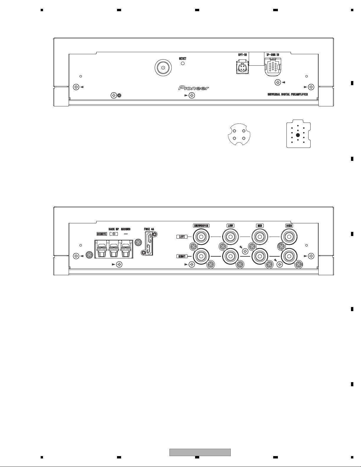
1. BUS+
2. BUSG
3. BUSG
4. BMUTE
5. BUS-
6. BUSG
IP-BUS INPUT
7. NC
8. ASENB
9. NC
10. NC
11. NC
1
2
3
4
8
9
10
11
5
6
7
1 : OPIG
2 : OPI
3 : GND
4 : OPI5V
4
2
3
1
OPTICAL INPUT
5.2 CONNECTOR FUNCTION DESCRIPTION
6. SERVICE MODE
There is not information to be shown in this chapter.
RS-P99/EW5
15
1234
1234
C
D
F
A
B
E
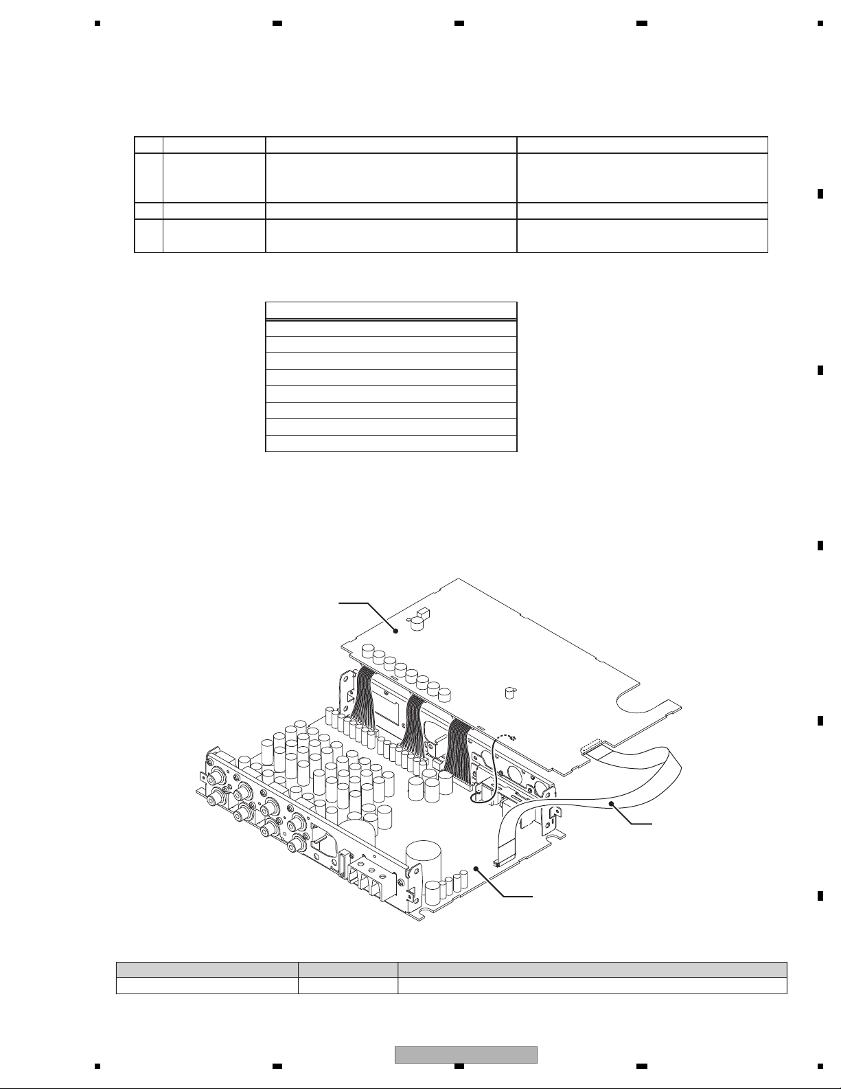
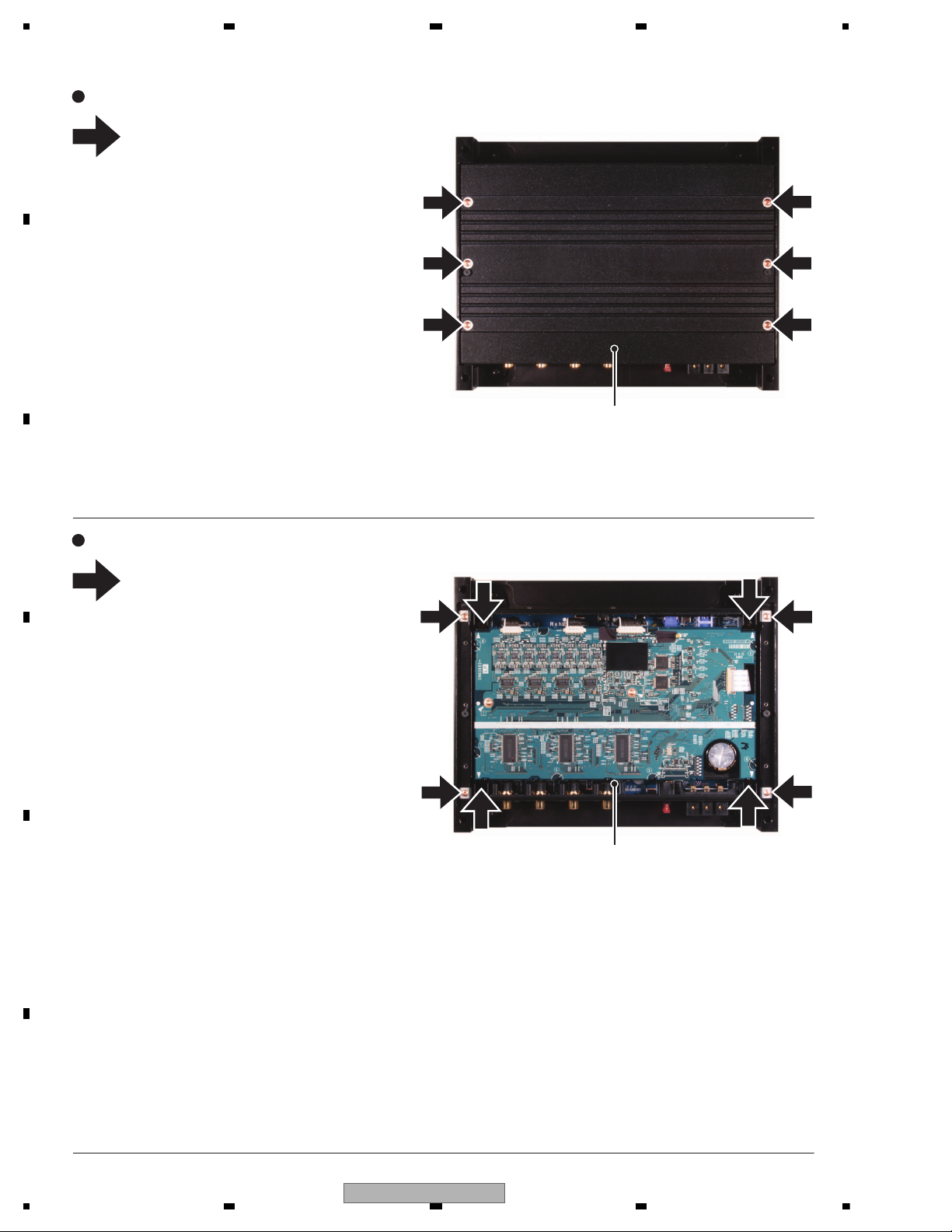
7. DISASSEMBLY
Removing the Lower Case (Fig.1)
Remove the six screws and then remove the
1
Lower Case.
1
1
1
1
1
1
Lower Case
Fig.1
Removing the Control Unit (Fig.2)
Remove the eight screws and then remove the
1
Control Unit.
1
1
1
1
1
1
1
1
Control Unit
Fig.2
16
RS-P99/EW5
5 678
56
7
8
C
D
F
A
B
E
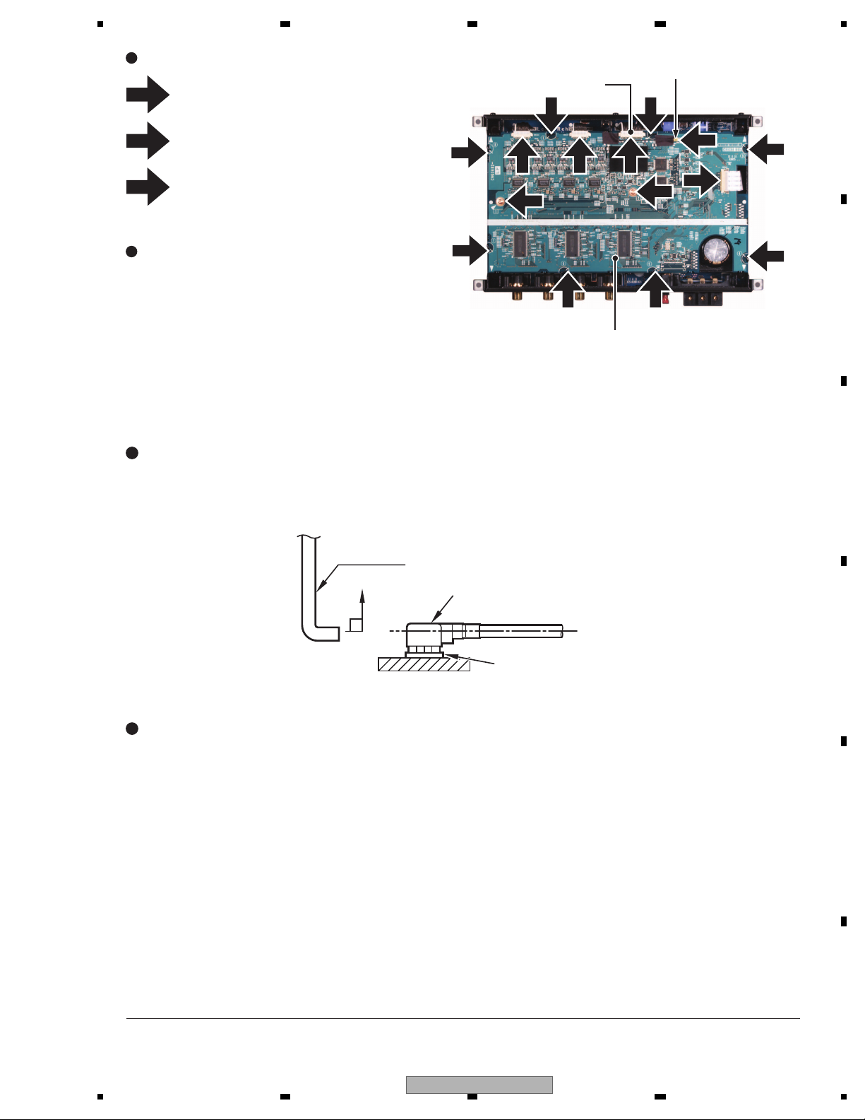
Removing the DSP Unit (Fig.3)
Disconnect the five connectors.
1
Remove the two screws.
2
14P Power Cable
3
1 1 1
3 3
Coaxial Jumper
1
3
Straighten the tabs at eight locations
3
indicated and then remove the DSP Unit.
Precaution for Disconnecting/Connecting the
14P Power Cable in DSP Unit
This connector has been built to fit more tightly
than other connectors. Please use due caution
not to cause damage when disconnecting or
2
2
3
3 3
1
3
connecting it.
DSP Unit
When unplugging the Coaxial Jumper, make sure to use jig GGF1539.
If the Coaxial Jumper is directly unplugged without using jig GGF1539, you might damage your fingertip or fingernail.
- -
How to Remove the Coaxial Jumper
- - When unplugging Coaxial Jumper, hook the point of jig GGF1539 on the lid of Coaxial Jumper
- - and vertically draw out along with the engagement axis of connector.
GGF1539
Coaxial Jumper
How to Attach the Coaxial Jumper
- -
Connector
- - For inserting Coaxial Jumper, adjust cord assy with the engagement axis of connector and insert it as vertically
- - as possible.
- - Do not insert the Coaxial Jumper in extreme slant, as the connector might suffer damage.
Fig.3
RS-P99/EW5
17
1234
1234
C
D
F
A
B
E
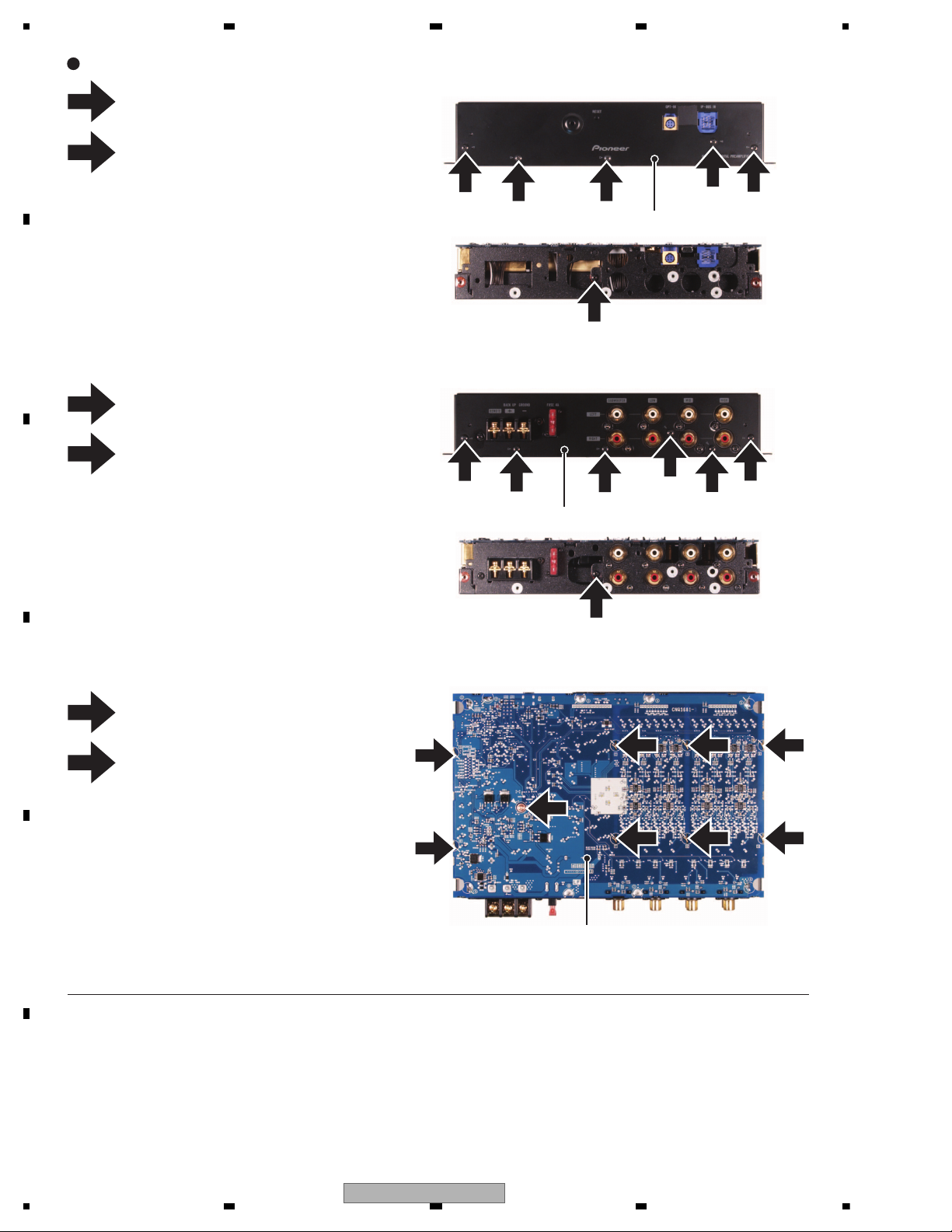
Removing the Control Unit (Fig.4)
(IP-BUS Side)
Remove the five screws and then remove
1
the Panel(IP-BUS Side).
Remove the screw.
2
1
1
1
1
1
Panel
2
(RCA Side)
Remove the six screws and then remove
3
the Panel(RCA Side).
Remove the screw.
4
3
3
3
3
3
3
Panel
4
Remove the screw.
4
Straighten the tabs at eight locations
5
indicated and then remove the Control Unit.
5
5
5
5
4
5
5
5
5
18
RS-P99/EW5
Control Unit
Fig.4
5 678
56
7
8
C
D
F
A
B
E
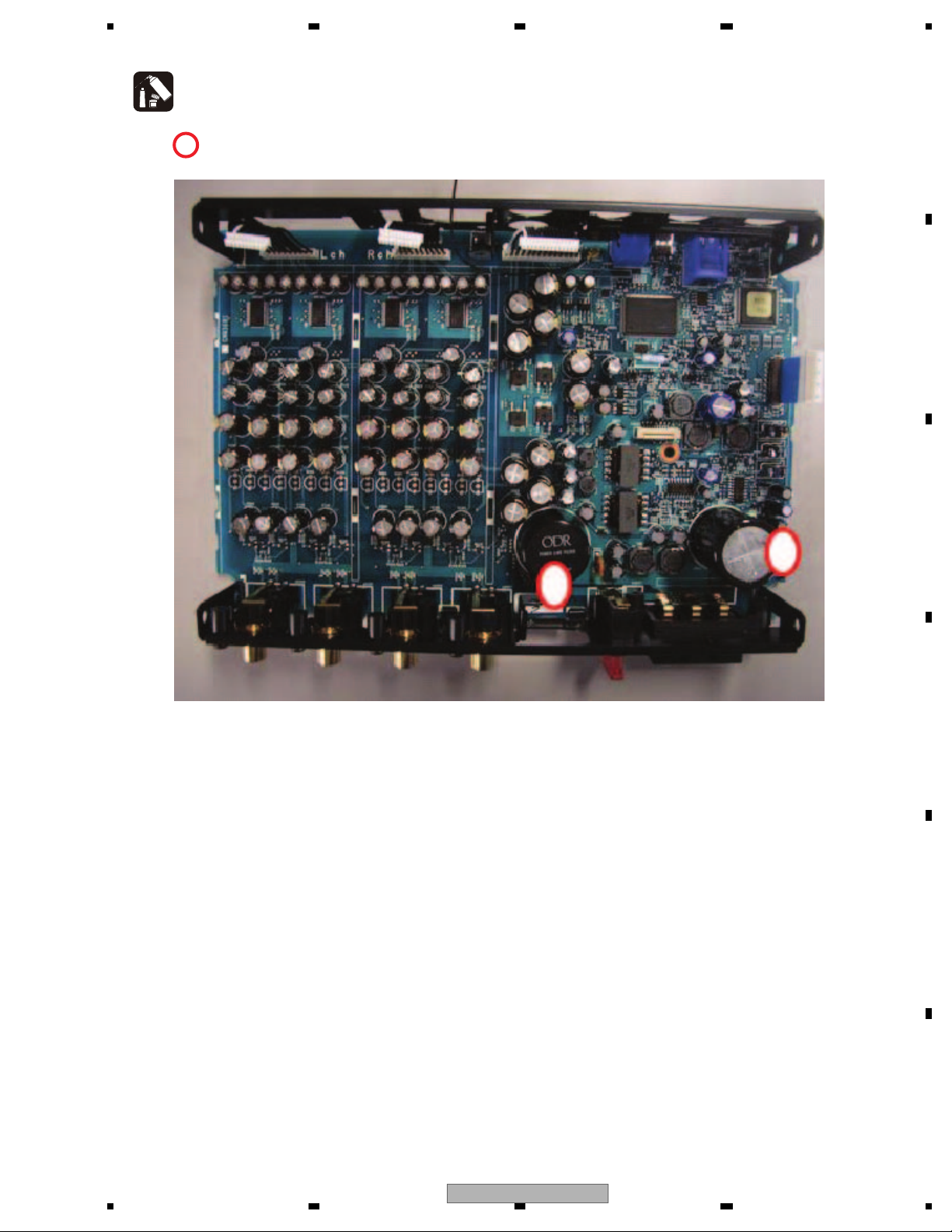
Bonding Position
: GEM1017
8. EACH SETTING AND ADJUSTMENT
There is not information to be shown in this chapter.
RS-P99/EW5
19
1234
1234
C
D
F
A
B
E
9. EXPLODED VIEWS AND PARTS LIST
NOTES : Parts marked by " * " are generally unavailable because they are not in our Master Spare Parts List.
The > mark found on some component parts indicates the importance of the safety factor of the part.
Therefore, when replacing, be sure to use parts of identical designation.
Screw adjacent to mark on the product are used for disassembly.
For the applying amount of lubricants or glue, follow the instructions in this manual.
(In the case of no amount instructions,apply as you think it appropriate.)
""
9.1 PACKING
20
RS-P99/EW5
5 678
56
7
8
C
D
F
A
B
E
PACKING SECTION PARTS LIST
Mark
Mark No. Description Part No.
1 Screw BNC50P250FTB
2 Cord CDE4167
3 Cord Assy CDE6642
4 Cable CDE6690
5 •••••
6 Cover CEG1057
7 Polyethylene Bag CEG1161
8 Unit Box CHG7379
9 Sub Unit Box CHG7380
10 Contain Box CHL7379
11 Protector CHP4057
No. Description Part No.
* 12 Shaft CLP1100
* 13 Shaft CLP1224
14 Clamper CNV1443
* 15 Polyethylene Bag E36-634
16 IM CD-ROM CPJ1313
17-1 Quick Start Guide CRD4501
17-2 Quick Start Guide CRD4502
* 17-3 Caution Card CRP1389
* 17-4 Caution Card CRP1423
* 17-5 Warranty Card CRY1279
> 18 Fuse(4 A) CEK1001
Quick Start Guide
Part No. Language
CRD4501 English, French, Italian, Spanish(Espanol)
CRD4502 German, Dutch, Russia
CONTENTS OF CD-ROM (Operation Manual), CPJ1313
Part No. Language
*CRB3380 English
*CRB3381 French
*CRB3382 Italian
*CRB3383 Spanish(Espanol)
*CRB3384 German
*CRB3385 Dutch
*CRB3386 Russia
All operation manuals are supplied in PDF files by the CD-ROM.
Regarding the availability of paper manual, contact Pioneer Service representative in your region.
RS-P99/EW5
21
 Loading...