

Page 1
ORDER NO.
CRT3659
RS-D7R — /EW5
SYSTEM CONTROL TUNER/CD OPTICAL DIGITAL REFERENCE SYSTEM
——
RS-D7R——
—
/EW5
This service manual should be used together with the following manual(s):
Model No. Order No. Mech.Module Remarks
CX-961 CRT2503 H2 CD Mech. Module : Circuit Descriptions, Mech. Descriptions, Disassembly
For details, refer to "Important Check Points for Good Servicing".
PIONEER CORPORATION 4-1, Meguro 1-chome, Meguro-ku, Tokyo 153-8654, Japan
PIONEER ELECTRONICS (USA) INC. P.O. Box 1760, Long Beach, CA 90801-1760, U.S.A.
PIONEER EUROPE NV Haven 1087, Keetberglaan 1, 9120 Melsele, Belgium
PIONEER ELECTRONICS ASIACENTRE PTE. LTD. 253 Alexandra Road, #04-01, Singapore 159936
PIONEER CORPORATION 2006
K-ZZW.OCT. 2006 Printed in Japan
Page 2
e
r
y
the
d
the
y
the
d
g
to
.
e
esults.
:
.
r
e
.
h
eter
abe
th
r
1234
SAFETY INFORMATION
This service manual is intended for qualified service technicians; it is not meant for the casual do-it-yourself
Qualified technicians have the necessary test equipment and tools, and have been trained to properly and safely repai
A
B
Improperl
ou
renotualified
Safety Precautions for those who Service this Unit
hen checking or adjusting the emitting power of the laser diode exercise caution in order to get safe, reliabl
r
ion
1. During repair or tests, minimum distance of 13 cm from the focus lens must be kept
2. During repair or tests, do not view laser beam for 10 seconds or longe
n
repair
safetyndreliability theroduct
thisroduct
roperlyn
ndmayvoi
ou
houldnotrisktryin
warrant
LASS 1 LASER PRODUCT
bottom of the playe
l
l is affixed to
CLASS 1
LASER PRODUCT
C
Specifications of Laser Diod
Specifications of laser radiation fields to which human access is possible during service
avelengt
- Service Precautions
1. You should conform to the regulations governing the product (safety, radio and noise, and other regulations),
and should keep the safety during servicing by following the safety instructions described in this manual.
D
2. Be careful in handling ICs. Some ICs such as MOS type are so fragile that they can be damaged by electrostatic
induction.
CD MECHANISM MODULE section precaution
1. Before disassembling the unit, be sure to turn off the power. Unplugging and plugging the connectors
during power-on mode may damage the ICs inside the unit.
2. To protect the pickup unit from electrostatic discharge during servicing, take an appropriate treatment
(short pin) by referring to "the DISASSEMBLY".
3. After replacing the pickup unit, be sure to check the grating.
nanom
E
F
2
1234
RS-D7R — /EW5
Page 3
5678
[Important Check Points for Good Servicing]
In this manual, procedures that must be performed during repairs are marked with the below symbol.
Please be sure to confirm and follow these procedures.
1. Product safety
Please conform to product regulations (such as safety and radiation regulations), and maintain a safe servicing environment by
following the safety instructions described in this manual.
1 Use specified parts for repair.
Use genuine parts. Be sure to use important parts for safety.
2 Do not perform modifications without proper instructions.
Please follow the specified safety methods when modification(addition/change of parts) is required due to interferences such as
radio/TV interference and foreign noise.
3 Make sure the soldering of repaired locations is properly performed.
When you solder while repairing, please be sure that there are no cold solder and other debris.
Soldering should be finished with the proper quantity. (Refer to the example)
4 Make sure the screws are tightly fastened.
Please be sure that all screws are fastened, and that there are no loose screws.
5 Make sure each connectors are correctly inserted.
Please be sure that all connectors are inserted, and that there are no imperfect insertion.
6 Make sure the wiring cables are set to their original state.
Please replace the wiring and cables to the original state after repairs.
In addition, be sure that there are no pinched wires, etc.
7 Make sure screws and soldering scraps do not remain inside the product.
Please check that neither solder debris nor screws remain inside the product.
8 There should be no semi-broken wires, scratches, melting, etc. on the coating of the power cord.
Damaged power cords may lead to fire accidents, so please be sure that there are no damages.
If you find a damaged power cord, please exchange it with a suitable one.
9 There should be no spark traces or similar marks on the power plug.
When spark traces or similar marks are found on the power supply plug, please check the connection and advise on secure
connections and suitable usage. Please exchange the power cord if necessary.
0 Safe environment should be secured during servicing.
When you perform repairs, please pay attention to static electricity, furniture, household articles, etc. in order to prevent injuries.
Please pay attention to your surroundings and repair safely.
A
B
C
D
2. Adjustments
To keep the original performance of the products, optimum adjustments and confirmation of characteristics within specification.
Adjustments should be performed in accordance with the procedures/instructions described in this manual.
3. Lubricants, Glues, and Replacement parts
Use grease and adhesives that are equal to the specified substance.
Make sure the proper amount is applied.
4. Cleaning
For parts that require cleaning, such as optical pickups, tape deck heads, lenses and mirrors used in projection monitors, proper
cleaning should be performed to restore their performances.
5. Shipping mode and Shipping screws
To protect products from damages or failures during transit, the shipping mode should be set or the shipping screws should be
installed before shipment. Please be sure to follow this method especially if it is specified in this manual.
56
RS-D7R — /EW5
E
F
7
8
3
Page 4

1234
CONTENTS
SAFETY INFORMATION..................................................................................................................................... 2
1. SPECIFICATIONS ............................................................................................................................................ 5
2. EXPLODED VIEWS AND PARTS LIST............................................................................................................ 6
A
B
C
2.1 PACKING ...................................................................................................................................................6
2.2 EXTERIOR(1) ............................................................................................................................................8
2.3 EXTERIOR(2) ..........................................................................................................................................10
2.4 CD MECHANISM MODULE..................................................................................................................... 12
3. BLOCK DIAGRAM AND SCHEMATIC DIAGRAM..........................................................................................14
3.1 BLOCK DIAGRAM ................................................................................................................................... 14
3.2 OVERALL CONNECTION DIAGRAM(GUIDE PAGE).............................................................................. 16
3.3 CD MECHANISM MODULE..................................................................................................................... 22
3.4 MASTER CLOCK UNIT ...........................................................................................................................26
3.5 KEYBOARD UNIT.................................................................................................................................... 28
4. PCB CONNECTION DIAGRAM ..................................................................................................................... 30
4.1 AUDIO CONTROL PCB........................................................................................................................... 30
4.2 CD CORE UNIT ....................................................................................................................................... 34
4.3 MASTER CLOCK UNIT ...........................................................................................................................36
4.4 KEYBOARD UNIT.................................................................................................................................... 38
4.5 OPT PCB AND SWITCH PCB ................................................................................................................. 40
5. ELECTRICAL PARTS LIST ............................................................................................................................ 41
6. ADJUSTMENT ............................................................................................................................................... 51
6.1 MASTER CLOCK ADJUSTMENT............................................................................................................ 51
6.2 CD ADJUSTMENT................................................................................................................................... 52
6.3 CHECKING THE GRATING AFTER CHANGING THE PICKUP UNIT .................................................... 54
6.4 ERROR MODE ........................................................................................................................................56
6.5 SYSTEM MICROCOMPUTER TEST PROGRAM ...................................................................................59
7. GENERAL INFORMATION ............................................................................................................................. 60
7.1 DIAGNOSIS ............................................................................................................................................. 60
7.1.1 DISASSEMBLY ..................................................................................................................................... 60
7.1.2 CONNECTOR FUNCTION DESCRIPTION.......................................................................................... 65
7.2 IC ............................................................................................................................................................. 66
7.3 OPERATIONAL FLOW CHART ............................................................................................................... 84
8. OPERATIONS ................................................................................................................................................ 85
D
E
F
4
1234
RS-D7R — /EW5
Page 5

5678
1. SPECIFICATIONS
General
Power source ..................................................... 14.4 V DC
(10.8 V to 15.1 V allowable)
Grounding system ........................................ Negative type
Max. current consumption .......................................... 4.0 A
Backup current ............................................... 5 mA or less
Dimensions
(mounting size)
..................178 (W) mm x 50 (H) mm x 160 (D) mm
(front face)
....................188 (W) mm x 58 (H) mm x 20 (D) mm
Weight ...................................................................... 1.6 kg
Digital input .................................................... Optical input
(Sampling frequency: 44.1 kHz to 96 kHz)
Digital output ................................................ Optical output
(Sampling frequency: 44.1 kHz)
CD player
System .................................... Compact disc audio system
Usable discs ................................................. Compact disc
Signal format ...................... Sampling frequency: 44.1 kHz
Number of quantization bits: 16; linear
Frequency characteristics ........ 5 Hz to 20 000 Hz (± 1 dB)
FM tuner
Frequency range ............................. 87.5 MHz to 108 MHz
Usable sensitivity ....................................................... 9 dBf
(0.8 µV/75 Ω, mono, S/N: 30 dB)
50 dB quieting sensitivity ........ 15 dBf (1.5 µV/75 Ω, mono)
Signal-to-noise ratio ........................ 70 dB (IEC-A network)
Distortion ........................... 0.3% (at 65 dBf, 1 kHz, stereo)
Frequency response .............. 30 Hz to 15 000 Hz (± 3 dB)
Stereo separation ......................... 40 dB (at 65 dBf, 1 kHz)
A
B
C
MW tuner
Frequency range ................. 531 kHz to 1 602 kHz (9 kHz)
Usable sensitivity ................................. 18 µV (S/N: 20 dB)
Selectivity .................................................. 50 dB (± 9 kHz)
LW tuner
Frequency range ................................. 153 kHz to 281 kHz
Usable sensitivity ................................. 30 µV (S/N: 20 dB)
Selectivity .................................................. 50 dB (± 9 kHz)
Infrared Remote Control
Wavelength ............................................... 940 nm ± 50 nm
Output ................................. typ; 12 nw/sr per Infrared LED
D
E
F
56
RS-D7R — /EW5
7
8
5
Page 6
N
1234
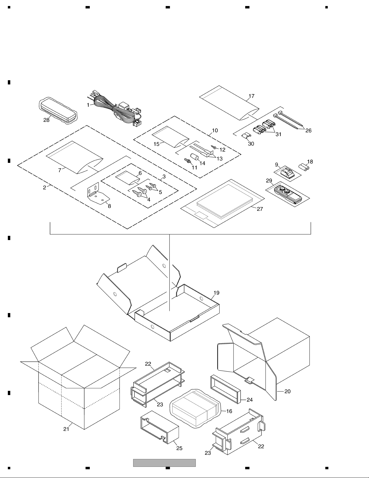
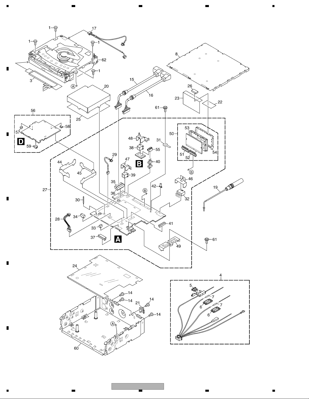
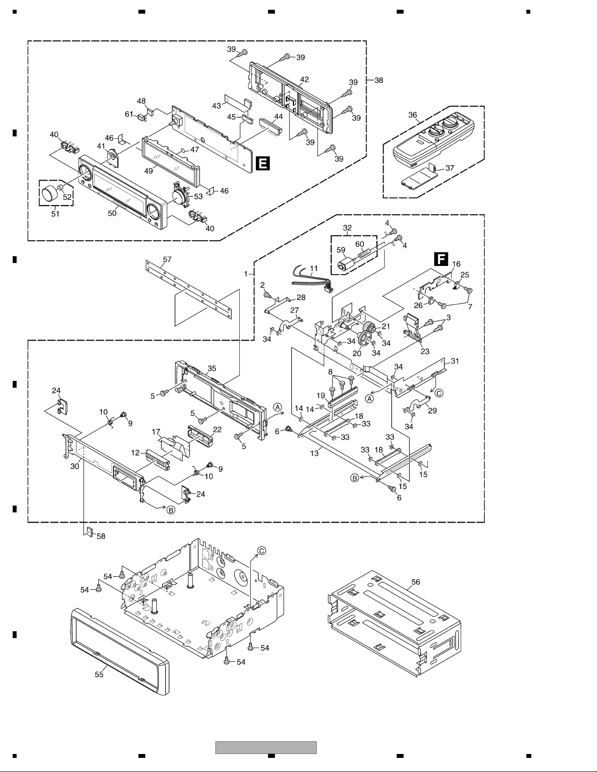
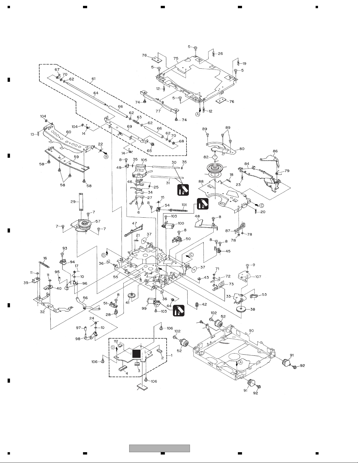
2. EXPLODED VIEWS AND PARTS LIST
OTES : • Parts marked by " * " are generally unavailable because they are not in our Master Spare Parts List.
• The > mark found on some component parts indicates the importance of the safety factor of the part.
A
Therefore, when replacing, be sure to use parts of identical designation.
• Screw adjacent to mark on the product are used for disassembly.
• For the applying amount of lubricants or glue, follow the instructions in this manual.
(In the case of no amount instructions,apply as you think it appropriate.)
2.1 PACKING
B
"
C
D
E
F
6
1234
RS-D7R — /EW5
Page 7

5678
PACKING SECTION PARTS LIST
Mark No. Description Part No.
1 Cord Assy CDE7598
2 Bracket Assy CEA2346
3 Screw Assy CZE3198
4 Screw BNC40P120FTB
5 Screw BPZ30P100FTB
* 6 Polyethylene Bag CEG-127
* 7 Polyethylene Bag CZE3201
8 Bracket CZN6467
9 Base Assy CEA2799
10 Accessory Assy CEA4784
A
11 Screw CBA1650
12 Screw CBA1921
13 Handle CNC5395
14 Bush CNV1917
* 15 Polyethylene Bag E36-615
16 Cover CEG1064
17 Polyethylene Bag CEG1161
* 18 Battery CEX1006
19 Sub Carton CHA3167
20 Carton CHG5897
21 Contain Box CHL5897
22 Protector CHP2383
23 Protector CHP2384
24 Protector CHP2385
25 Protector CHP2386
* 26 Lock Tie CNV-754
27-1 Owner's Manual(English) CRB2206
27-2 Owner's Manual(Spanish) CRB2207
27-3 Owner's Manual(German) CRB2208
27-4 Owner's Manual(French) CRB2209
27-5 Owner's Manual(Italian) CRB2210
27-6 Owner's Manual(Dutch) CRB2211
27-7 Owner's Manual(Russian) CRB2212
* 27-8 Caution Card CRP1332
* 27-9 Passport CRY1013
B
C
D
* 27-10 Warranty Card CRY1157
27-11 Polyethylene Bag CEG1116
28 Case Assy CXB3520
29 Remote Control Assy CXC3398
30 Filter CTX1054
31 Filter CTX1060
56
RS-D7R — /EW5
E
F
7
8
7
Page 8
1234
2.2 EXTERIOR(1)
A
B
C
D
E
F
8
1234
RS-D7R — /EW5
Page 9

5678
EXTERIOR(1) SECTION PARTS LIST
Mark No. Description Part No.
1 Screw BSZ26P050FCU
2 •••••
3 Flat Cable CDE6627
4 Cord Assy CDE7598
> 5 Fuse(4 A) CEK1001
6 Cap CNS1472
7 Resistor RS1/2PMF102J
8 Case CNB2991
9 •••••
10 •••••
11 •••••
12 •••••
13 •••••
14 Screw BSZ26P050FCU
15 Cord CDE4107
16 Cord CDE4108
17 Cord CDE6684
18 •••••
19 Antenna Cord CDH1251
20 Shield CNC9688
21 Holder CND2224
22 Seal CNM7598
23 Insulator CNM8845
24 Insulator CNM8846
25 Insulator CNM8850
Mark No. Description Part No.
50 FM/AM Tuner Unit CWE2027
51 Connector(CN1) CKS4276
52 Connector(CN2) CKS4276
53 Holder(SH1) CNC8708
54 Case CNC8713
55 Connector(CN173) HKS-193
56 Master Clock Unit CWN1766
57 Connector(CN1551) CKS4977
58 Connector(CN1502) CKS4977
59 Connector(CN1501) CKS4979
60 Chassis Unit CXC7221
61 Screw ISS26P055FTC
62 CD Mechanism Module(H2) CXK5358
A
B
C
26 Spacer CNM8852
27 Audio Control Unit CWN2000
28 Connector(CN353) CDE6681
29 Cord(CN321) CDE8126
30 Clamper CEF1041
31 Terminal(CN401) CKF1064
32 Connector(CN901) CKM1500
33 Plug(CN652) CKS-783
34 Plug(CN851) CKS-786
35 Plug(CN101) CKS1044
36 Plug(CN102) CKS1045
37 Connector(CN801) CKS1085
38 Connector(CN172) CKS1940
39 Connector(CN171) CKS2600
40 Connector(CN174) CKS5184
41 Connector(CN651) CKS4865
42 Mini Pin Jack(CN451) CKX1046
43 •••••
44 Holder CNC9186
45 Holder CNC9187
46 Holder CNC9188
47 Holder CNC9451
48 Holder CNC9452
49 Holder CNC9556
D
E
F
56
RS-D7R — /EW5
7
8
9
Page 10
1234
2.3 EXTERIOR(2)
A
B
C
D
E
F
10
1234
RS-D7R — /EW5
Page 11

5678
EXTERIOR(2) SECTION PARTS LIST
Mark No. Description Part No.
1 Panel Assy CXC7351
2 Screw BMZ20P030FTC
3 Screw BPZ20P060FTC
4 Screw(M2 x 3) CBA1061
5 Screw(M2 x 3) CBA1931
6 Screw CBA1933
7 Screw(M2 x 7) CBA1938
8 Screw(M1.4 x 4) CBA1942
9 Screw CBA1946
10 Spring CBH2445
11 Cord CDE5960
12 Connector CKS4436
13 Frame CNC8201
14 Spacer CNM6155
15 Spacer CNM6156
16 PCB CNP5941
17 Flexible PCB CNP6124
18 Guide CNV5696
19 Rack CNV5697
20 Gear CNV5698
21 Torque Limit Unit CNV5762
22 Cover CNV6573
23 Lighting Conductor CNV6574
24 Holder CNV6575
25 Switch(S951) CSN1012
Mark No. Description Part No.
50 Sub Grille Assy CXC6141
51 Knob Unit(VOLUME) CXC6209
52 Spring CBL-108
53 Button assy(SELECT) CXC6210
54 Screw(M2 x 2.5) CBA1609
55 Panel CNS8708
56 Holder CNC8659
57 Cover CNM9146
58 Cushion CNN1687
59 Motor CXM1217
60 Gear CNV5761
61 IC(IC1881) TSOP4840SB1
A
B
C
26 Switch(S952) CSN1022
27 Arm Unit CXB3574
28 Bracket Unit CXB3577
29 Arm Unit CXB3866
30 Holder Unit CXB6726
31 Frame Unit CXB6727
32 Motor Unit(M10) CXC2489
33 Washer 2-1816-0035-D2-00
34 Washer 2-1821-0045-D2-00
* 35 Panel CNS8707
36 Remote Control Assy CXC3398
37 Lower Case CNS8028
38 Detach Grille Assy CXC6140
39 Screw BPZ20P100FTB
40 Button CAC6862
41 Cushion CNM7548
* 42 Cover CNS8709
43 Flat Cable CDE6700
44 Connector(CN1881) CKS4435
45 Connector(CN1861) CKS5640
46 Spacer CNM7397
47 Seal CNM7549
48 Spacer CNM9191
49 OEL Module MXK8203
D
E
F
56
RS-D7R — /EW5
7
8
11
Page 12
1234
2.4 CD MECHANISM MODULE
A
B
83
85
111
C
GEM1030
GEM1030
D
GEM1029
E
108
109
C
110
F
12
1234
RS-D7R — /EW5
Page 13

5678
CD MECHANISM MODULE SECTION PARTS LIST
Mark No. Description Part No.
1 CD Core Unit CWX3369
2 Connector(CN101) CKS4939
3 Connector(CN901) CKS5248
4 Connector(CN701) CKS5091
5 Screw BSZ20P035FTC
6 Screw(M2 x 4) CBA2037
7 Screw(M2 x 2.5) CBA1974
8 Screw(M2 x 3) CBA1762
9 Screw(M2 x 6.2) CBA1763
10 Washer CBF1037
11 Washer CBF1064
12 Spring CBH2291
13 Spring CBH2292
14 Spring CBH2293
15 Spring CBH2295
16 Spring CBH2297
17 Spring CBH2298
18 Spring CBH2299
19 Spring CBH2303
20 Spring CBH2304
21 Spring CBH2305
22 Spring CBH2308
23 Spring CBH2309
24 Spring CBH2332
25 Spring CBH2416
26 Spring CBH2434
27 Spring CBL1448
28 Spring CBL1466
29 Connector CDE6099
30 Shaft CLA3683
31 Shaft CLA3684
32 Lever CNC8501
33 Bracket CNC8507
34 Bracket CNC8509
35 Cushion CNM6301
36 Sheet CNM6773
37 Sheet CNM6774
38 Gear CNR1559
39 Arm CNV5928
40 Arm CNV5929
41 Gear CNV5930
42 Gear CNV5932
43 Gear CNV5931
44 Gear CNV5933
45 Holder CNV5943
46 Holder CNV5944
47 Arm CNV5948
48 Cover CNV5950
49 Holder CNV5951
50 Holder CNV6222
51 Holder CNV6223
52 Damper CNV6426
53 Holder CNV6446
54 Holder CNV6512
55 Chassis Unit CXB4501
56 Arm Unit CXB4503
57 Motor Unit(M3) CXC6003
56
Mark
RS-D7R — /EW5
No. Description Part No.
58 Screw(M2 x 1.2) CBA1760
59 Guide CNV5925
60 Arm Unit CXB5311
61 Loading Arm Assy CXB5715
62 Washer CBF1060
63 Spring CBH2170
* 64 Shaft CLA3678
* 65 Gear CNV5934
66 Roller CNV6068
67 Holder CNV6210
68 Collar CNV6439
69 Arm Unit CXB5686
70 Washer YE20FTC
71 Washer CBF1038
72 Arm CNC8498
73 Lever Unit CXB4502
74 Screw(M2 x 1.5) CBA1761
75 Frame CNC9417
76 Sheet CNM6951
77 Guide CNV5924
78 Washer CBF1037
79 Spring CBH2300
80 Spring CBL1446
81 •••••
82 Spacer CNM6467
83 Spacer CNR1189
84 Guide CNV5945
85 Clamper CNV6767
86 Arm CNV5947
87 Lever CNV5949
88 Arm Unit CXB4505
89 Screw JFZ20P020FTC
90 Frame CNC9416
91 Damper CNV6426
92 Screw ISS20P060FTC
93 Screw(M2 x 3) CBA1762
94 Holder CNV6341
95 Roller CNV6389
96 Arm Unit CXB5970
97 Roller CNV6389
98 Armunit CXB5971
99 Load Motor Assy(M2) CXC5821
100 Carriage Motor Assy(M1) CXC5819
101 Screw Unit(-B) CXB6363
102 Screw ISS20P060FTC
103 Screw JFZ20P025FNI
104 Washer YE15FUC
105 Pickup Unit(Service)(P8) CXX1305
106 Screw IMS20P030FTC
* 107 Cover CNC9151
108 Screw BMZ26P030FTC
109 Cord CDE8349
110 Spacer CNM7805
111 Sheet CNC9466
112 Connector(CN301) CKS4439
7
8
A
B
C
D
E
F
13
Page 14
7
B
S
1
1234
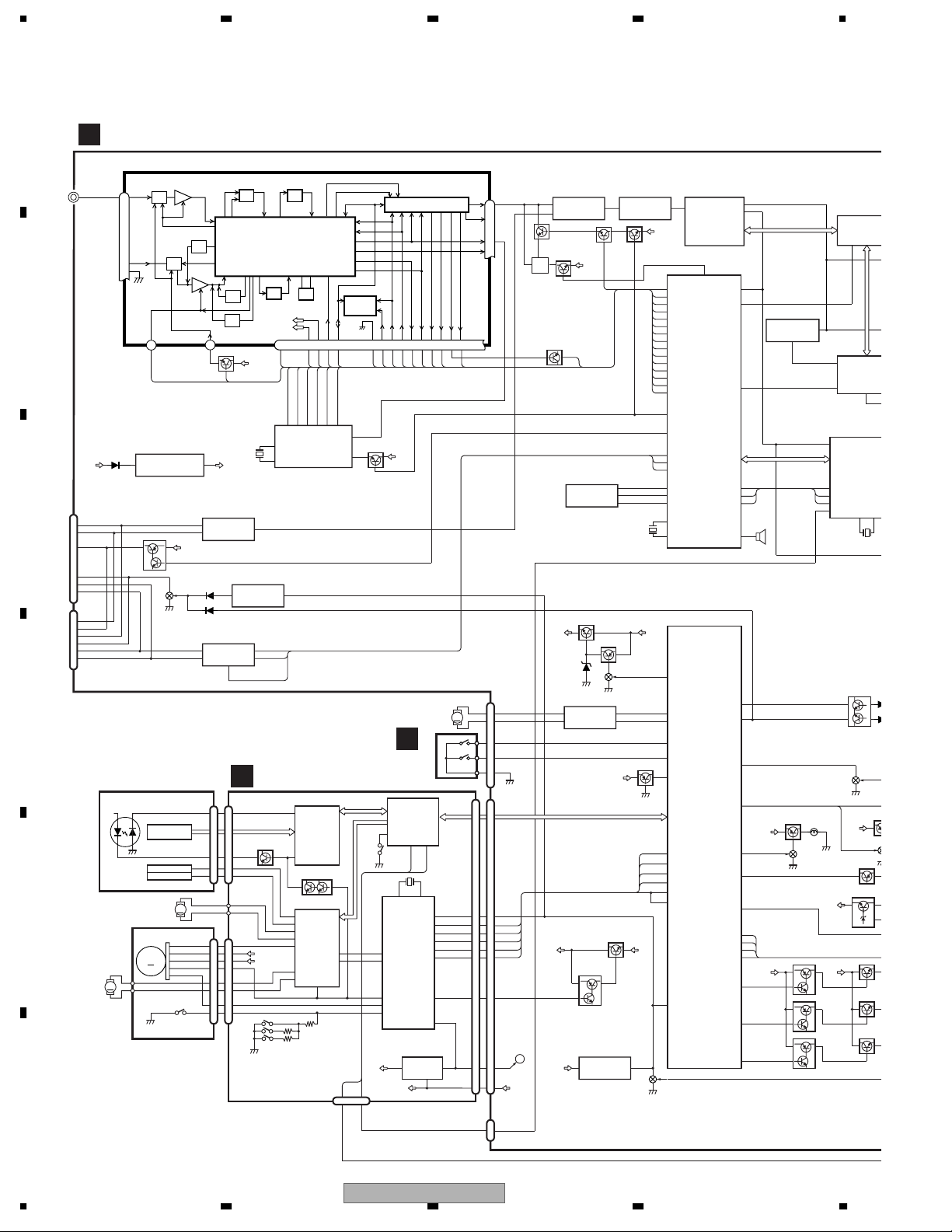
3. BLOCK DIAGRAM AND SCHEMATIC DIAGRAM
3.1 BLOCK DIAGRAM
A
AUDIO CONTROL PCB
A
FM/AM TUNER UNIT
CN451
CN451
MAIN
ANT
AMANT
28
ATT
FMANT
27
RFGND
26
B
LOCH
23
IC 401
BUP
C
7
11
8
4
5
1
CN101
BUSL1
BUSL2
ASENB1
2
S-812C50AUA-C3E
Q101
Q102
Q103
CN102
11
8
7
4
BUS+
1
BUS-
5
D
PICKUP UNIT(SERVICE)(P8)
MONITOR
DIODE
+5V
HOLOGRAM
UNIT
LASER
DIODE
FOCUS ACT.
TRACKING ACT.
CARRIAGE
E
LOADING
MOTOR
MOTOR
SPINDLE
MOTOR
M
M
F
AMRF
ATT
M
EC
VM
VCC
FG
CLAMPSW
ANT ADJ
BUP
FM/AM 1ST IF 10.7 MHz
T51 Q51 CF51
MIXER, IF AMP, DET.
FMRF
IMG ADJ
AM 2ND IF
RF ADJ
LOCL
Q401
SYS+8
X501
3.648MHz
VDD
1
2
IP-BUS DRIVER
6
5
HA12187FPS1
MD
LD(–)
FO+
TO+
3
IC 102
TA2050S
INVERTER
42
IC 103
TC7S04FU
12TX
IC 101
8
CD CORE UNIT
C
CN101
5
AC/F/E/BD
Q101
17
4
3
CN901
9
VD
7
V+5
12
CONTST/SP
10
1
2
3
4
11
6
CF52 CF53
MPXREF 41 kHz
IC1
CF202
X901
10.25 MHz
450 kHz
VDD
VCC
CREQ
DI/DO
NCNCWC
222510 14 12 15 16 8 13 3
19
20177
rck
RDT
ldet
drst
rdslk
RDS57K
15
678
45
RDS DECODER
11
IC 501
PM4009A1
12
RX
IPPW
RF AMP
8
MDI
IC 201
TA2153FNS1
9
LDO
Q102
13
11
15
IC 401
16
BA5811FM
22
10
9
MUTE
21
AMDET
EEPROM
FMLOCL
1
2
MCK
1
IC3
NC
924
20
24
HOME
SW
TX
4
DGND
CE2CKCE1
11
COMP
Q501
AUTOMATIC FLAP
MOTOR AND SENSE
SWITCH
PCB
TC9495F2S1
66
HOME
9
X2
PE5238A1
4
CDLOAD
5
CDEJET
3
CONT
73
SPDIFG
58
DSCSNS
V+5
CN301
IC 2 FM MPX
SDBWSLFMSD
FM/AM
VDD
F
IC 301
DOUT
978
TX
MCK
X601
10
X1
IC 601
CD5VON
+5V
REGULATOR
IC 801
4
BA05SFP
2
VD
L ch
6
R ch
5
COMP
21
LDET
18
STIND
NL1
NL2
1
42
CN851
5
M
4
3
2
1
CN701
CN651
XI
RESET
7
52
77
1
29
2
31
BRXEN
VDCONT
1
CD5VON
BSRQ
BRST
BSCK
BDATA
20
20
15
15
16
16
17
17
18
18
19
19
VDCONT48
5
5
13
13
VD
8
8
CN652
CDTX
1
2
4
BA3131FS
Q151
Q154
Q153
Q402
NL2
VCC
3
14
BUP
A
VDD
VD
21
71
IC 121
PDH098A
IC 851
BA6288FS
Q155
LDET
VDD
1
IC 602
2
3
12.58291MHz
Q851
Q852
Q853
6
11
VDD
Q998
Q991
RESET
IC 961
S-80834CNUA-B8T
NJM4580M
X601
IC 122
FM/AM
Q601
1
Q962
ADC
166MCK1
IC 201
PCM1800S1
VDD
Q156
59
TMUTE
79
NL1
58
NL2DT
60
SDBW
37
TUNPCE2
74
SL
94
TUNPDI
97
TUNPCK
39
ST
38
CONTROLLER
SD
99
TUNPCE
57
CURRQ
IC 601 (1/2)
88
LDET
PE5208A1
35
LOCL
36
LOCH
98
TUNPDO
29
FM/AM
28
ASENBO
86
TX
85
RX
27
IPPW
33
ROMCS
32
ROMCK
31
ROMDATA
16
X1
15
X2
BUP
SYSTEM
CONTROLLER
22
FLPPWR
IC 601 (2/2)
PE5208A1
43
FLPOPN
42
FLPCLS
45
FCLSSW
44
FOPNSW
83
AVREF
70
BSRQ
69
BRST
65
BSCK
68
BRXEN
67
BSO
66
BSI
VD
11
RESET
SYSTEM
DGMUTE
SYSPWR
dgrst
DSEL
AUDIO
DERR
DIRSEL
ASENS
BSENS
ISENS
ELPILM
TELIN
DALMON
ROT0
ROT1
OELPW
SWVDD
ILMPWR
PEE
RXD
TXD
46
52
IC 264
TC7SH02FUS1
4
47
26
7
53
SP641
100
92
93
91
21
Q804
BUP
Q805
23
4
71
95
96
63
64
BUP BUP
25
1
24
Q808
Q802
Q807
2
63
22
47
dgrst
LC89055WH
24
AUDIO
34
DERR
1
DIRSEL
4
CDTX
VDD
SELECTO
IC 251
TC74HCT15
1
MCK1
SRC
IC 261
SM5849
DMUTE
6
DIR
IC 221
NIX
23 22
X221
12.288MHz
Q931
Q932
BUP
Q951
Q911
Q803
Q801
Q806
DOUT/BCKO/LRCO
XOUT
Q
Q174
14
1234
RS-D7R — /EW5
Page 15
5678
A
64
2FUS1
4
Q808
Q802
Q807
SELECTOR
IC 251
TC74HCT157AF
1
2
63
MCK1
SM5849BF
22
DMUTE
47
dgrst
IC 221
LC89055WHS-RA8
24
AUDIO
34
DERR
1
DIRSEL
4
CDTX
12.288MHz
Q931
Q932
BUP
VDD
BUP
4
9
7
DOUT/BCKO/LRCO
24
IC 302
TC7SET04FUS1
SRC
IC 261
2
DI
6
42
3
DINO
DIR
13
2
NIX
23 22
X221
XOUT
DATA0
1417
EF 901
Q173
3
IC 173
Q912
NJM78L05UA
BUP
Q174
Q951
Q911
Q803
Q801
Q806
DIT
7
6
IC 301
4
TC9271FS
14
IC 172
TC7SET08FUS1
IC 263
TC7SH08FUS1
IC 281
PD0236BM
18
1
VCC
4
16
12
TC7WH04FU
4
IC 262
TC7WH34FU
3
8
A
6 1 BREM
TPD1018F
IC 322
TC7S04FU
IC 171
Q171
5V
SYS+B
BUP
IC 941
2
OPT IN
5
Q971
Q921
Q923
Q922
Q172
SYS+B
SWD+B
CN321
CN174
CN171
CN353
CD5VON
CN901
BUP2
CN801
KYDT
DPDT
OELB
SWVDD
RST1
TEL1
1
OPT PCB
B
CN173
2
2
CN172
2
OPT OUT
B
MASTER CLOCK UNIT
D
Q1551
3
IC 1551
NJM431U
1
2
4
3
IC 1552
NJM2373AF
+8V
4
Q1502
CD5VON
3
CN1501
IC 1503
NJM431U
ACC
4
2
CEK1001
4A
3
ILL
1
6
5
KEYBOARD UNIT
E
CN1881
KYDT
13
4
DPDT
12
5
OELB
15
2
SWDVDD
8
9
ILB
ILB
13
4
RESRT
15
2
SWDVDD
5
2
Q1501
Q1504
3
1
SWDVDD
SWDVDD
KEY
MATRIX
VDD
3
IC 1881
TSOP4840SB1
REMOTE CONTROL
SENSOR
Q1554
ACC
BACKUP
ILL
MUTE
1
Q1506
GND
B.REM
Q1555
IC 1502
NJM431U
Q1881
X1801
3.77MHz
OPT IN
1
25
26
64
81
80
45
IC 1553
2
NJM2373AF
Q1503
3
Q1505
IC 1504
NJM431U
1,3
KEYDT
DSPDT
X1
X0
IC 1801
PD6556A
REMIN
IC 1888
S-93C46BD0I-J8
Q1552
5
Q1507
VCC
75 4
CPU_RESET
70 2
OEL_WR
67 2
OEL_RESET
72
7
Q1553
SWDVDD
X1511
16.9344MHz
X1501
16.9344MHz
S-80929CNNB-G8Z
TC7SET08FUS1
TC7SET08FUS1
TC7SET08FUS1
5
S-818A33AUC-BGN
MAX4412EXK
IC 1501
TC7SU04FU
IC 1802
IC 1884
IC 1885
IC 1886
IC 1887
TC74VHCT541AFK
IC 1821
PD8166A
IC 1883
IC1555
3
2
4
4
4
1
CN1551
CN1502
CN1861
SWDVDD
23,33
14
1
42
1
1
2
17
18
22
19
C
D
E
OEL MODULE
F
56
RS-D7R — /EW5
7
8
15
Page 16
A-a
A-b
1234
3.2 OVERALL CONNECTION DIAGRAM(GUIDE PAGE)
Note: When ordering service parts, be sure to refer to " EXPLODED VIEWS AND PARTS LIST" or
"ELECTRICAL PARTS LIST".
A
Large size
A-b
A-b
SCH diagram
Guide page
CN701
C
A-a
A-a
A-a
C
CN301
A-b
Detailed page
A-a
B
FM(100%): -7.8dBs
IP-BUS
(MCD, MDVD):-+2.2dBs
AM(30%):-17.8dBs
IP-BUS: -1.8dBs
C
AM(30%):-30dBs
FM(100%):-20dBs
CWE2027
D
MAIN ANTENNA
E
CN1881
E
F
M
M10
AUTOMATIC
FLAP MOTOR
CXC2489
OPEN
CLOSE
S952
CSN1022
S951
CSN1012
SWITCH PCB
F
A F
16
1234
RS-D7R — /EW5
Page 17
5678
A
A-b
OPT PCB
B
AUDIO CONTROL PCB
A
AUDIO CONTROL UNIT
Consists of
AUDIO CONTROL PCB
OPT PCB
CN1501
B
D
CN1551
D
>
CEK1001
4A
BACKUP
ILL
GND
ACC
MUTE
>
B.REM
C
D
PCB
E
CN1881
NOTE :
Symbol indicates a resistor.
No differentiation is made between chip resistors and
discrete resistors.
Symbol indicates a capacitor.
No differentiation is made between chip capacitors and
discrete capacitors.
Decimal points for resistor
and capacitor fixed values
are expressed as :
2.2 2R2
0.022 R022
RS-D7R — /EW5
56
>
E
The > mark found on some component parts indicates
the importance of the safety factor of the part.
Therefore, when replacing, be sure to use parts of
←
←
identical designation.
F
A B
7
8
17
Page 18
1234
A
CN1501
D
AUDIO CONTROL UNIT
Consists of
AUDIO CONTROL PCB
B
OPT PCB
CN1551
D
C
AUDIO CONTROL PCB
A
A-a A-b
D
E
OPT PCB
B
F
A-b
18
123
B
RS-D7R — /EW5
1234
Page 19
5678
>
BACKUP
4A
CEK1001
ILL
GND
ACC
MUTE
B.REM
A
B
The > mark found on some component parts indicates
the importance of the safety factor of the part.
Therefore, when replacing, be sure to use parts of
identical designation.
←
←
>
Decimal points for resistor
and capacitor fixed values
are expressed as :
2.2 2R2
0.022 R022
C
>
A-a A-b
D
Symbol indicates a resistor.
No differentiation is made between chip resistors and
discrete resistors.
Symbol indicates a capacitor.
No differentiation is made between chip capacitors and
discrete capacitors.
NOTE :
E
4
RS-D7R — /EW5
56
F
A-b
881
7
8
19
Page 20
W
1234
A
B
C
A-b
B
123
IP-BUS: -1.8dBs
AM(30%):-17.8dBs
FM(100%): -7.8dBs
CN301
C
A-bA-a
D
CN701
C
E
F
A-a
20
E2027
(MCD, MDVD):-+2.2dBs
IP-BUS
AM(30%):-30dBs
FM(100%):-20dBs
RS-D7R — /EW5
1234
Page 21
5678
4
A
A-b
CN1881
E
SWITCH PCB
F
S951
CSN1012
S952
CSN1022
OPEN
CLOSE
M
AUTOMATIC
M10
CXC2489
FLAP MOTOR
B
C
CWE2027
A-bA-a
D
E
MAIN ANTENNA
56
RS-D7R — /EW5
F
A-a
7
8
F
21
Page 22
1234
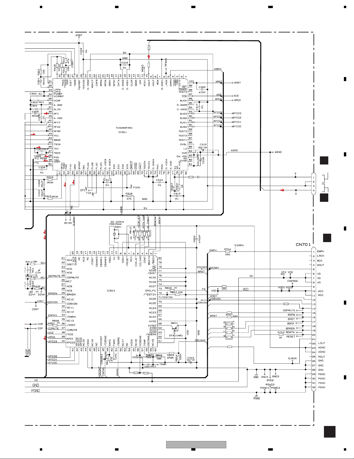
3.3 CD MECHANISM MODULE
A
PICKUP UNIT(SERVICE)(P8)
F
SL
T
B
T
F
SL SL
F
T
F
T
CD CORE UNIT
C
F
SL
F
T
F
T
RF AMP
SL
SL
SL
F
SL
T
T
F
F
SL
T
T
SL
4
!
5
T
F
8200P
F
T
330K
SL
F
T
6
T
C
CARRIAGE MOTOR
M1 CXC5819
SL
SIGNAL LINE
F
FOCUS SERVO LINE
T
TRACKING SERVO LINE
C
D
SWITCHES:
CD CORE UNIT
S901 :LOAD,EJ SWITCH . . . . ON-OFF
S902, 903 :LOAD,EJ SWITCH . . . . ON-OFF
S904
The underlined indicates the switch position.
CARRIAGE SERVO LINE
S
SPINDLE SERVO LINE
:HOME SWITCH . . . . . . ON-OFF
C
C
RED
BLACK
WHITE
C
C
F
T
C
2
7
1
#
F
T
ACT / MOTOR DRIVE
3
F
T
S
C
C
)
S
S
9
T
T
F
5V
LOADING MOTOR
E
M2 CXC5821
SPINDLE MOTOR
M3 CXC6003
S
S
0
REGULATOR
S
F
C
S
C
C
S
F
C
22
1234
RS-D7R — /EW5
Page 23
5678
TX
0R0
R321
33P
220K
330K
0P
SL
SERVO CONTROL / DSP / DAC / LPF
SL
220
R311
A
B
F
T
F
T
CN301
C314
R305
220P
4R7K
S
C
(
@
TX
8
MCK
SL
TX
D
CN1502
MCK
GND
GND
TX
A
C
CN652
S
C
A
CN651
)
VDCONT
⁄
R713
CSENS
PE5238A1
CD MECH. CONTROLLER
S
R605
R606
22K
47K
DSPMUTE
BSRQ
BSCK
BRXEN
BDATA
SUBOK
R702
R711
R701
220
220
0R0
R708
0R0
CSENS
XRST
CD5VON
DSPMUTE
BSRQ
BRST
BSCK
BRXEN
BDATA
RESET
SUBOK
D
E
56
RS-D7R — /EW5
F
C
7
8
23
Page 24
1234
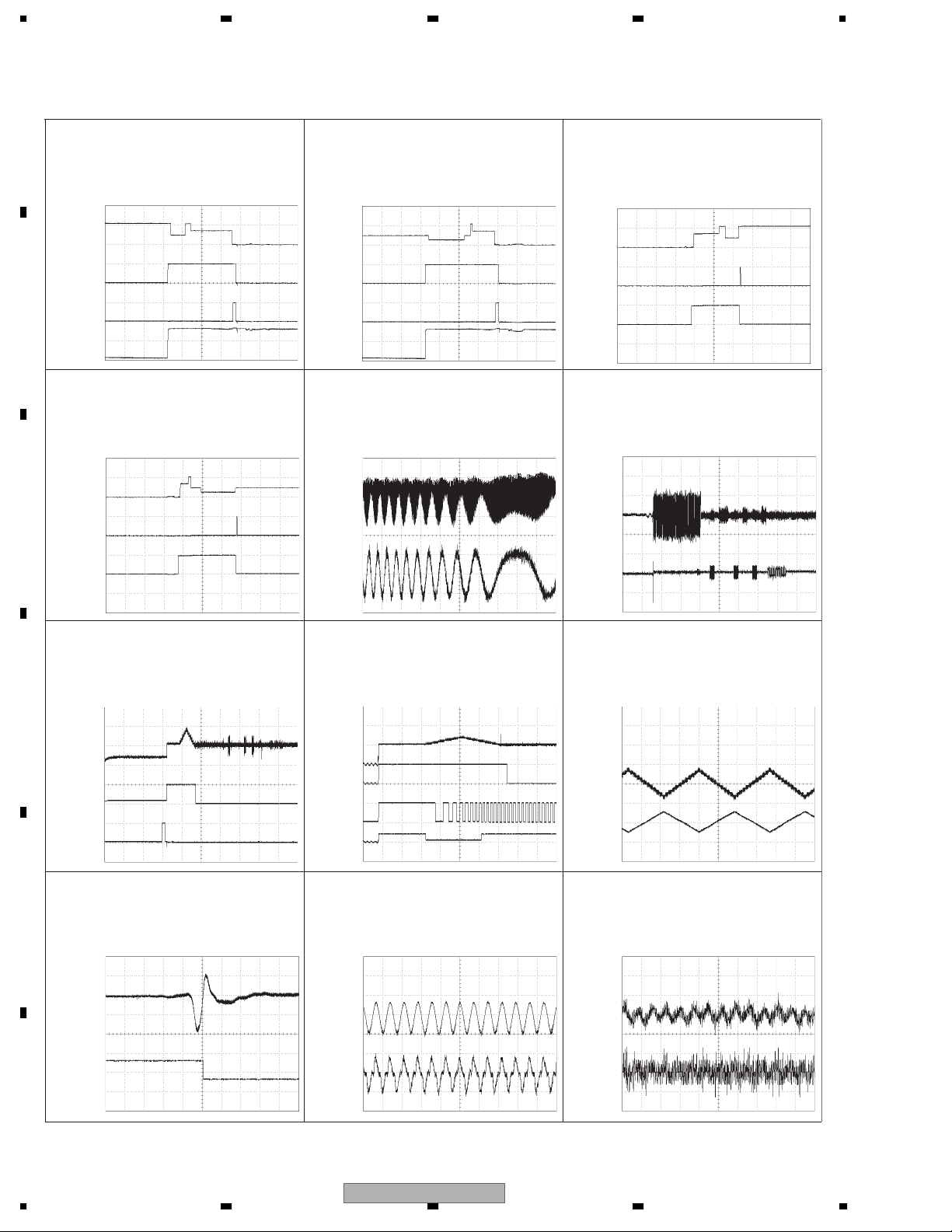
- Waveforms
A
1 CH1:DSCSNS 5 V/div.
2 CH2:CDLOAD 5 V/div.
3 CH3:CDEJET 5 V/div.
⁄ CH4:VD 5 V/div.
8 cm LOAD
500 ms/div.
Note:1. The encircled numbers denote measuring pointes in the circuit diagram.
2. Reference voltage
VREF:2.1 V
1 CH1:DSCSNS 5 V/div.
2 CH2:CDLOAD 5 V/div.
3 CH3:CDEJET 5 V/div.
500 ms/div.
1 CH1:DSCSNS 5 V/div.
2 CH2:CDLOAD 5 V/div.
3 CH3:CDEJET 5 V/div.
500 ms/div.
⁄ CH4:VD 5 V/div.
12 cm LOAD
8 cm EJECT
→
GND
→
GND
B
GND
GND
→
→
1 CH1:DSCSNS 5 V/div.
2 CH2:CDLOAD 5 V/div.
3 CH3:CDEJET 5 V/div.
12 cm EJECT
→
GND
C
→
GND
→
GND
7 CH1:FD 1 V/div.
8 CH2:fok 5 V/div.
9 CH3:SINY 5 V/div.
Setup
D
500 ms/div.
500 ms/div.
→
GND
→
GND
→
GND
→
GND
4 CH1:RFO 500 mV/div.
5 CH2:TEY 500 mV/div.
Tracking open
→
VREF
→
VREF
7 CH1:FD 2 V/div.
8 CH2:fok 5 V/div.
0 CH3:FG 5 V/div.
9 CH4:SINY 5 V/div.
Setup(In focus)
2 ms/div.
100 ms/div.
→
GND
→
GND
→
GND
5 CH1:TEY 500 mV/div.
6 CH2:FEY 500 mV/div.
Setup
→
VREF
→
VREF
7 CH1:FD 1 V/div.
! CH2:FOP 2 V/div.
Setup(In focus)
200 ms/div.
200 ms/div.
→
VREF
→
VREF
→
VREF
6 CH1:FEY 500 mV/div.
@ CH2:foon 5 V/div.
E
Setup(Focus close)
→
VREF
→
VREF
F
24
1234
1 ms/div.
→
VREF
→
VREF
→
VREF
→
VREF
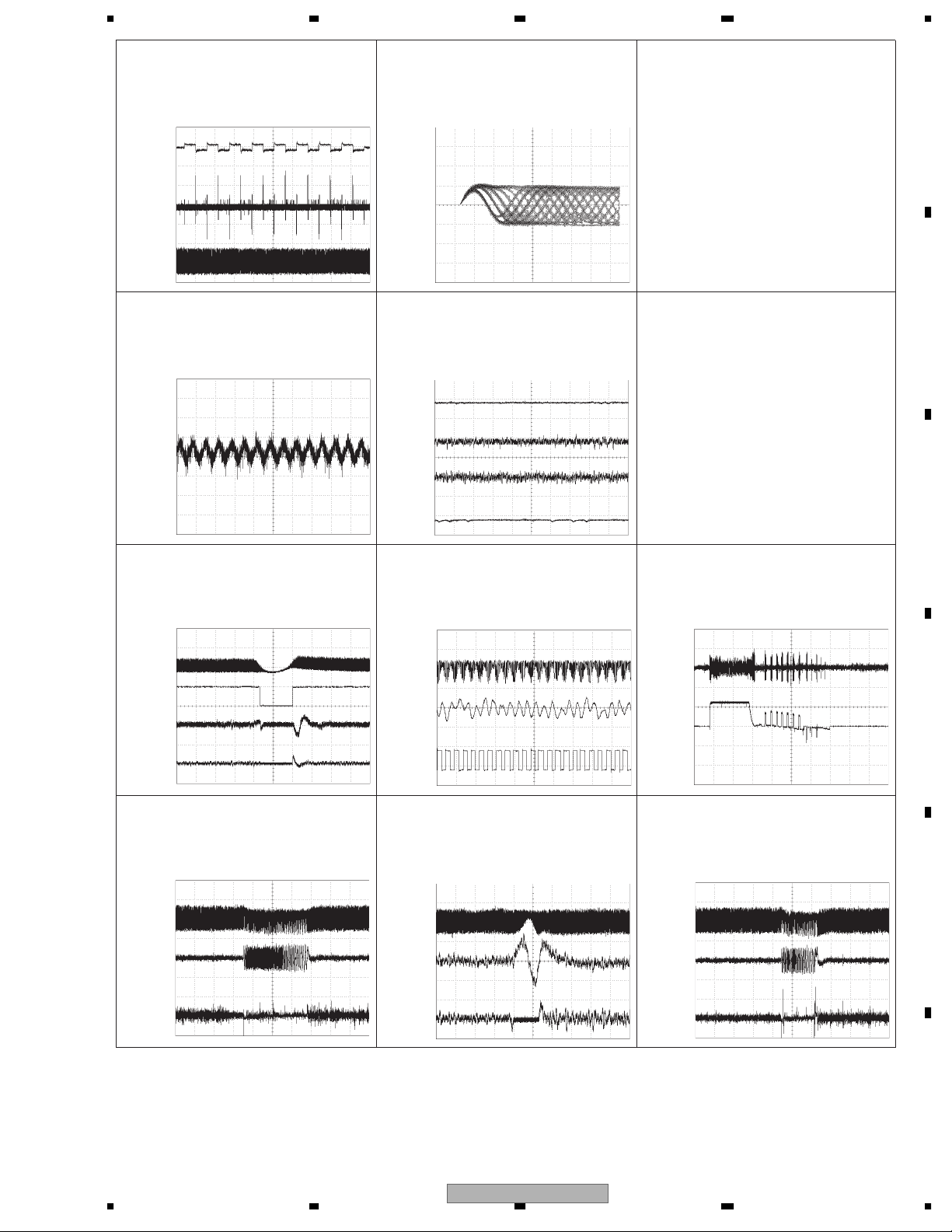
6 CH1:FEY 200 mV/div.
7 CH2:FD 500 mV/div.
Setup(Focus AGC)
→
VREF
→
VREF
RS-D7R — /EW5
1 ms/div.
→
VREF
→
VREF
5 CH1:TEY 200 mV/div.
# CH2:TD 200 mV/div.
Setup(Tracking AGC)
→
VREF
→
VREF
1 ms/div.
Page 25
5678
6 CH1:FEY 500 mV/div.
7 CH2:FD 500 mV/div.
4 CH3:RFO 1 V/div.
Setup(FE Bias adjustment)
→
VREF
→
VREF
→
VREF
9 CH1:SINY 100 mV/div.
Play
→
VREF
10 ms/div.
200 ms/div.
4 CH1:RFO 0.5 V/div.
Play
→
VREF
6 CH1:FEY 500 mV/div.
7 CH2:FD 500 mV/div.
5 CH3:TEY 500 mV/div.
# CH4:TD 500 mV/div.
Play
→
VREF
→
VREF
→
VREF
0.5 µs/div.
A
B
1 ms/div.
4 CH1:RFO 2 V/div.
( CH2:dfct 5 V/div.
7 CH3:FD 1 V/div.
# CH4:TD 2 V/div.
Play(The defect part passes)
→
VREF
→
VREF
→
VREF
→
VREF
4 CH1:RFO 1 V/div.
5 CH2:TEY 1 V/div.
# CH3:TD 1 V/div.
Test mode 100TRjump
→
VREF
→
VREF
500 µs/div.
5 ms/div.
→
VREF
4 CH1:RFO 1 V/div.
5 CH2:TEY 500 mV/div.
( CH3:dfct 5 V/div.
CRG move
→
VREF
→
VREF
→
VREF
4 CH1:RFO 1 V/div.
5 CH2:TEY 500 mV/div.
# CH3:TD 1 V/div.
Test mode 1TRjump
→
VREF
→
VREF
50 µs/div.
500 µs/div.
5 CH1:TEY 500 mV/div.
) CH2:CIN 500 mV/div.
Search
→
VREF
→
VREF
4 CH1:RFO 1 V/div.
5 CH2:TEY 1 V/div.
# CH3:TD 1 V/div.
Test mode 32TRjump
→
VREF
→
VREF
C
200 ms/div.
D
5 ms/div.
E
VREF
→
VREF
→
RS-D7R — /EW5
56
→
VREF
F
7
8
25
Page 26
1234
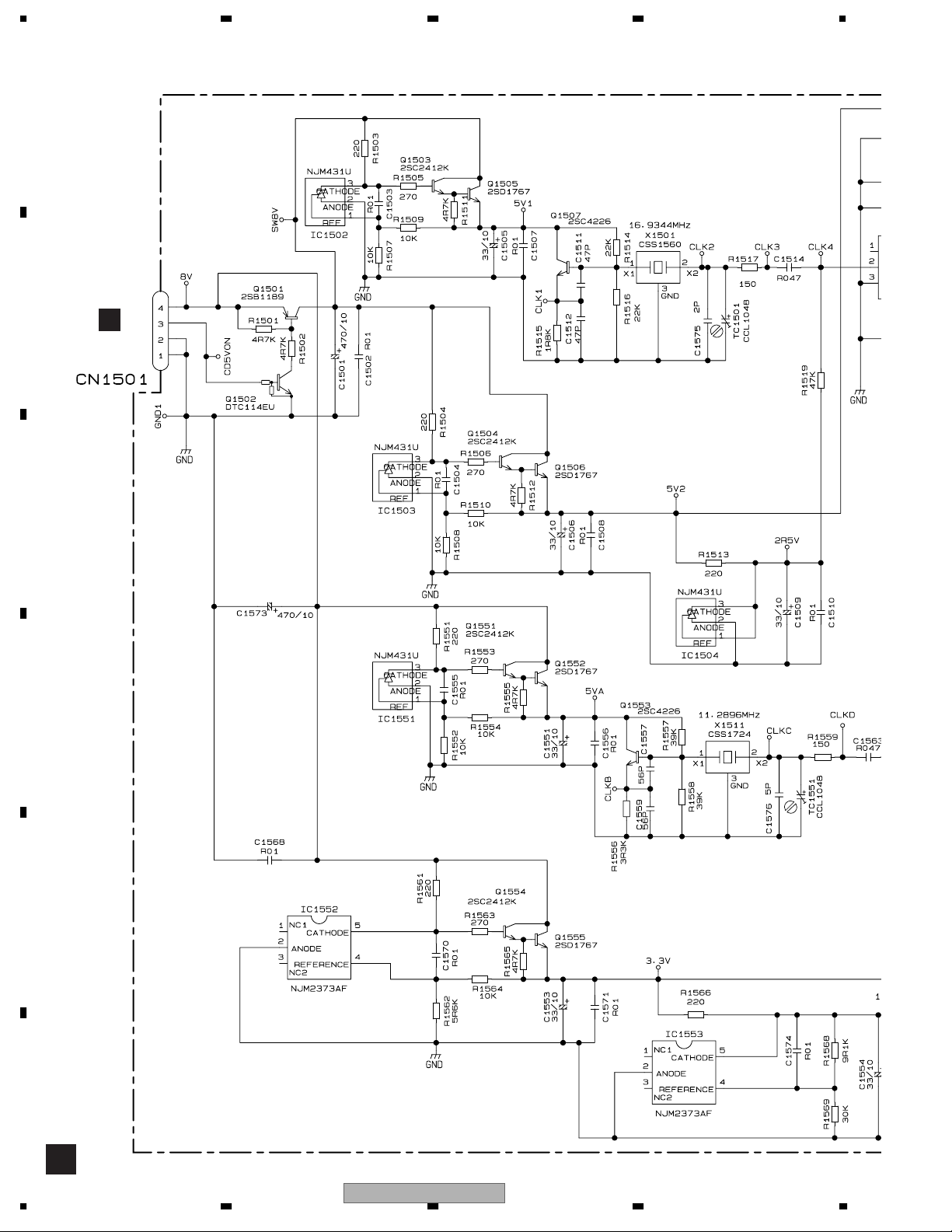
3.4 MASTER CLOCK UNIT
A
B
C
D
A
CN353
E
F
D
26
1234
RS-D7R — /EW5
Page 27
5678
A
MASTER CLOCK UNIT
D
C
CN301
B
A
CN321
C
D
E
56
RS-D7R—/EW5
F
D
7
8
27
Page 28

1234
3.5 KEYBOARD UNIT
A
CN801
A
B
VOLUME
C
D
E
OEL Module
MXK8203
F
E
28
1234
RS-D7R—/EW5
Page 29

5678
KEYBOARD UNIT
E
A
B
C
EL Module
MXK8203
D
E
F
56
RS-D7R—/EW5
E
7
8
29
Page 30

1234
0
A
4. PCB CONNECTION DIAGRAM
4.1 AUDIO CONTROL PCB
A
B
C
NOTE FOR PCB DIAGRAMS
1.The parts mounted on this PCB
include all necessary parts for
several destination.
For further information for
respective destinations, be sure
to check with the schematic dia gram.
2.Viewpoint of PCB diagrams
Connector
P.C.Board
A
Capacitor
Chip Part
AUDIO CONTROL PCB
SIDE A
SIDE B
140
130
120
110
100
90
B
CN173
OPT IN
1
3
2
4
IP-BUS IN
FM/
IP-BUS OUT
80
70
CN1551
D
D
60
50
40
E
30
CN1501
D
20
10
F
F
M10
A
30
1234
Y
0
10 20 30 40 50 60 70 8
X
RS-D7R—/EW5
Page 31

5678
FM/AM TUNER UNIT
MAIN ANTENNA
11
A
SIDE A
CORD ASSY
B
C
C
CN701
D
E
CN301
C
E
FRONT
70 80 90 100 110 120 130 140 150 160 170
56
RS-D7R—/EW5
7
CN1881
8
F
A
31
Page 32

1234
A
11
B
TESTIN
AUDIO CONTROL PCB
A
PCL
C
D
E
F
890100110120130140150160170
32
A
RS-D7R—/EW5
1234
Page 33

5678
SIDE B
1
140
A
130
120
B
110
100
90
C
80
70
60
50
40
30
20
D
E
56
RS-D7R—/EW5
10
Y
F
102030405060708090
X
7
0
8
A
33
Page 34

1234
4.2 CD CORE UNIT
A
B
C
CD CORE UNIT
C
IC,Q
LOAD, EJ
SIDE A
LOAD, EJ
HOME
D
E
E
F
C
34
1234
RS-D7R—/EW5
Page 35

5678
A
CN651
CD CORE UNIT
C
1
LOAD, EJ
A
SIDE B
IC,Q
B
M2 LOADING MOTOR
M3 SPINDLE MOTOR
C
A
D
CN652
CN1502
VREF1
E
F
PICKUP UNIT
(SERVICE)(P8)
D
M1 CARRIAGE MOTOR
E
F
56
RS-D7R—/EW5
C
7
8
35
Page 36

1234
4.3 MASTER CLOCK UNIT
MASTER CLOCK UNIT
D
A
CN301
C
80
B
70
60
C
SIDE A
CN321
A
50
40
D
30
20
E
10
Y
0
X
F
10 20 30 40 50 60 70
CN353
A
D
36
1234
RS-D7R—/EW5
Page 37

5678
MASTER CLOCK UNIT
D
CLKO
SIDE B
80
70
60
A
B
C
CLKA
50
40
D
30
20
E
10
56
RS-D7R—/EW5
10203040506070
0
X
F
D
7
8
37
Page 38

1234
4.4 KEYBOARD UNIT
KEYBOARD UNIT
A
B
E
40
30
20
VOLUME
10
SOURCE
DISPLAY
RESET
Y
C
0
E
0
D
X
KEYBOARD UNIT
X
10 20 30 40 50 60 70 80
10 20 30 40 50 60 70 80
Y
10
20
E
30
40
F
E
38
1234
RS-D7R—/EW5
Page 39

5678
SIDE A
A
B
EJECT
BAND
80 90 100 110 120 130 140 150 160
80 90 100 110 120 130 140 150 160
C
SIDE B
D
E
OEL MODULE
A
RS-D7R—/EW5
56
CN801
7
F
E
8
39
Page 40

1234
4.5 OPT PCB AND SWITCH PCB
OPT PCB
A
CN174
A
B
OPT OUT
C
OPT PCB
B
SIDE BSIDE A
SWITCH PCB
F
D
BLUE
A
RED
WHITE
CN851
OPEN
S952
E
F
CLOSE
S951
BBF
40
1234
RS-D7R—/EW5
Page 41

5678
N
5. ELECTRICAL PARTS LIST
OTE:
• Parts whose parts numbers are omitted are subject to being not supplied.
• The part numbers shown below indicate chip components.
Chip Resistor
RS1/_S___J,RS1/__S___J
Chip Capacitor (except for CQS.....)
CKS....., CCS....., CSZS.....
• The > mark found on some component parts indicates the importance of the safety factor of the part.
Therefore, when replacing, be sure to use parts of identical designation.
• Meaning of the figures and others in the parentheses in the parts list.
Example) IC 301 is on the point (face A, 91 of x-axis, and 111 of y-axis) of the corresponding
PC board.
IC 301 (A, 91, 111) IC NJM2068V
A
B
Circuit Symbol and No. Part No.
Unit Number : CWN2000
Unit Name : Audio Control Unit
Unit Number : CWN1766
Unit Name : Master Clock Unit
Unit Number :
Unit Name : Keyboard Unit
Unit Number :
Unit Name : Switch PCB
Unit Number : CWX3369
Unit Name : CD Core Unit
Audio Control Unit
Consists of
Audio Control PCB
OPT PCB
AB
Unit Number : CWN2000
Unit Name : Audio Control Unit
MISCELLANEOUS
IC 101 (A,38,128) IC HA12187FPS1
IC 102 (A,29,121) IC TA2050S
IC 103 (A,42,118) IC TC7S04FU
IC 121 (A,45,96) IC BA3131FS
IC 122 (B,56,97) IC NJM4580M
IC 171 (A,39,134) IC TC7WH04FU
IC 172 (A,44,137) IC TC7SET08FUS1
IC 173 (A,48,137) IC NJM78L05UA
IC 201 (A,44,82) IC PCM1800S1
IC 221 (A,72,41) IC LC89055WHS-RA8
IC 251 (A,59,75) IC TC74HCT157AF
IC 261 (A,79,78) IC SM5849BF
IC 262 (A,83,62) IC TC7WH34FU
Circuit Symbol and No. Part No.
IC 263 (A,82,56) IC TC7SH08FUS1
IC 264 (A,57,68) IC TC7SH02FUS1
IC 281 (A,71,62) IC PD0236BM
IC 301 (A,60,85) IC TC9271FS
IC 302 (A,52,71) IC TC7SET04FUS1
IC 322 (A,34,71) IC TC7S04FU
IC 401 (A,65,129) IC S-812C50AUA-C3E
IC 501 (A,75,98) IC PM4009A1
IC 601 (A,118,95) IC PE5208A1
IC 602 (A,102,83) IC PDH098A
IC 851 (A,48,11) IC BA6288FS
IC 941 (B,140,116) IC TPD1018F
IC 961 (A,110,112) IC S-80834CNUA-B8T
Q 101 (A,8,114) Transistor 2SA1037K
Q 102 (A,8,111) Transistor DTC124EUA
Q 103 (B,9,115) Transistor 2SC4081
Q 121 (B,32,95) Transistor IMD2A
Q 151 (B,64,129) Transistor 2SD1757K
Q 152 (B,56,129) Transistor 2SD1757K
Q 153 (B,57,120) Transistor IMH3A
Q 154 (A,57,119) Transistor DTA114EU
Q 155 (B,91,142) Transistor 2SC4081
Q 156 (B,78,142) Transistor DTA124EUA
Q 171 (A,40,142) Transistor 2SC2412K
Q 172 (B,39,132) Transistor 2SC4453
Q 173 (A,46,129) Transistor 2SB1238
Q 174 (B,42,124) Transistor DTC114EU
Q 261 (A,69,21) Transistor 2SD1767
Q 301 (B,58,90) Transistor DTC114EU
Q 401 (B,107,142) Transistor 2SC4081
Q 402 (B,69,143) Transistor 2SC2412K
Q 501 (A,68,114) Transistor DTA123EU
Q 601 (B,126,101) Transistor DTA114EU
Q 801 (A,153,12) Transistor 2SD1760F5
Q 802 (B,149,13) Transistor IMD2A
Q 803 (A,140,29) Transistor 2SD2396
Q 804 (A,103,12) Transistor 2SB1238
Q 805 (A,96,13) Transistor DTC124EUA
Q 806 (A,103,17) Transistor 2SD1859
Q 807 (B,96,18) Transistor IMD2A
Q 808 (B,129,35) Transistor IMD2A
C
D
E
F
56
RS-D7R—/EW5
7
8
41
Page 42

1234
Circuit Symbol and No. Part No.
Q 851 (A,65,9) Transistor 2SD1760F5
Circuit Symbol and No. Part No.
L 173 (B,42,139) Inductor LCYC100K2125
Q 852 (B,63,11) Transistor DTA114EU
A
Q 853 (B,73,14) Transistor DTC124EUA
Q 911 (A,141,87) Transistor 2SD1760F5
Q 912 (B,143,91) Transistor IMD2A
Q 921 (A,140,40) Transistor 2SD2396
Q 922 (B,131,53) Transistor DTC114EU
Q 923 (A,135,49) Transistor 2SB1243
Q 931 (B,126,113) Transistor IMX1
Q 932 (B,126,110) Transistor DTC114EU
Q 951 (B,125,117) Transistor 2SA1576A
Q 962 (B,114,116) Transistor 2SC4081
Q 971 (A,140,63) Transistor 2SD2396
B
Q 991 (B,126,74) Transistor IMD2A
Q 998 (A,140,74) Transistor 2SD2396
D 101 (A,42,121) Diode DAN202U
D 102 (B,42,120) Diode 1SS355
D 171 (B,31,143) Diode 1SS352
D 221 (B,80,51) Diode Network DA204U
D 222 (B,76,51) Diode Network DA204U
D 261 (A,63,23) Diode HZS4LL(A)
D 262 (B,80,71) Diode Network DA204U
D 263 (B,80,67) Diode Network DA204U
D 264 (B,72,80) Diode Network DA204U
C
D 265 (B,72,76) Diode Network DA204U
D 281 (B,74,58) Diode Network DA204U
L 174 (B,36,132) Inductor CTF1407
L 201 (A,52,83) Inductor CTF1305
L 202 (A,52,85) Inductor CTF1305
L 221 (A,83,19) Inductor LCTAW1R0J3225
L 222 (A,83,23) Inductor LCTAW1R0J3225
L 251 (A,67,71) Inductor CTF1305
L 261 (A,60,38) Inductor LCTAW1R0J3225
L 262 (B,79,64) Inductor CTF1305
L 263 (B,76,67) Inductor CTF1305
L 264 (A,85,56) Inductor CTF1305
L 265 (A,57,65) Inductor CTF1305
L 281 (B,61,63) Inductor LCYC1R0K2125
L 301 (A,58,92) Inductor LCTAW1R0J3225
L 302 (B,56,64) Inductor LCYC100K2125
L 322 (A,34,67) Inductor LCYC100K2125
L 401 (A,70,131) Inductor LAU2R2K
L 402 (A,116,130) Ferri-Inductor LAU4R7K
L 404 (A,98,125) Chip Coil LCTAW1R0J4532
L 430 (B,70,119) Inductor CTF1295
L 501 (A,65,101) Inductor LCTAW100J3225
L 503 (A,65,96) Inductor LCTAW101J3225
L 504 (A,72,114) Inductor CTF1305
L 601 (A,134,98) Chip Coil LCTAW100J2520
L 602 (A,132,97) Inductor LCTAW2R2J2520
L 604 (A,133,104) Inductor LCTAW2R2J2520
D 282 (B,74,61) Diode Network DA204U
D 401 (A,63,121) Diode ERA15-02VH
D 402 (A,66,122) Diode HZS16(2)
D 801 (B,120,35) Diode Network DA204U
D 802 (B,120,26) Diode Network DA204U
D 803 (B,120,29) Diode Network DA204U
D 804 (B,120,23) Diode Network DA204U
D 805 (B,155,12) Diode MA3056(M)
D 806 (A,134,29) Diode HZS9L(C2)
D
D 807 (B,120,32) Diode Network DA204U
D 808 (A,116,19) Diode Network DA204U
D 810 (B,115,24) Diode MA3062(M)
D 811 (A,103,20) Diode HZS9L(C2)
D 812 (A,93,7) LED NECWB205-5780
D 851 (A,57,14) Diode HZS7L(C3)
D 852 (A,23,11) Diode 1SS133
D 853 (A,26,11) Diode 1SS133
D 901 (A,148,130) Diode ERA15-02VH
D 911 (A,148,95) Diode ERA15-02VH
D 912 (A,134,87) Diode HZS6L(B1)
E
D 921 (A,134,43) Diode HZS9L(B3)
D 922 (B,125,55) Diode DAN202U
D 931 (A,140,104) Diode HZS7L(A1)
D 932 (A,143,104) Diode HZS7L(C3)
D 933 (A,136,104) Diode ERA15-02VH
D 943 (A,149,104) Diode ERA15-02VH
D 944 (A,153,104) Diode ERA15-02VH
D 951 (B,126,120) Diode DAN202U
D 961 (B,114,113) Diode 1SS355
D 972 (A,131,61) Diode HZS6L(B1)
F
D 991 (A,133,76) Diode HZS9L(B1)
L 101 (A,38,123) Inductor LCTC3R3K2125
L 171 (A,35,144) Inductor LCTC2R7K2125
L 172 (A,32,144) Inductor LCYC1R0K2125
42
1234
RS-D7R—/EW5
L 605 (A,130,104) Inductor LCTAW2R2J2520
L 651 (A,124,70) Inductor LAU2R2K
L 801 (A,137,11) Inductor CTF1614
L 802 (A,126,28) Inductor CTF1489
L 951 (A,146,104) Inductor LAU2R2K
X 221 (A,70,51)
X 501 (A,86,95) Radiator 3.648 MHz CSS1500
X 601 (A,102,94) Radiator 12.5829 MHz CSS1495
>FU911 (A,134,94) Fuse 200 mA CEK1247
>FU971 (A,116,59) Fuse 400 mA CEK1250
SP641 (A,77,11) Buzzer CPV1062
EF901 (A,166,111) EMI Filter CCG1175
ZNR451 (A,129,141) Surge Protector DSP-201M-A21F
FM/AM Tuner Unit CWE2027
Crystal Resonator 12.288 MHz
CSS1416
RESISTORS
R 101 (A,32,129) RS1/10S101J
R 102 (B,21,128) RS1/10S620J
R 103 (A,32,126) RS1/10S101J
R 104 (A,7,119) RS1/10S152J
R 105 (A,35,124) RS1/16S103J
R 106 (A,10,111) RS1/10S562J
R 107 (A,10,114) RS1/16S332J
R 109 (B,21,122) RS1/16S181J
R 110 (B,21,117) RS1/16S181J
R 111 (B,22,111) RS1/16S223J
R 112 (B,22,118) RS1/16S223J
R 113 (B,21,111) RS1/16S102J
R 114 (B,22,123) RS1/16S102J
R 115 (A,10,120) RD1/4PU560J
R 116 (B,42,117) RS1/16S472J
R 117 (B,9,112) RS1/16S224J
R 118 (A,41,123) RS1/16S681J
Page 43

5678
Circuit Symbol and No. Part No.
R 119 (A,41,124) RS1/16S681J
R 121 (B,37,97) RS1/16S622J
R 122 (B,45,97) RS1/16S622J
R 123 (B,38,94) RS1/16S392J
R 124 (B,46,94) RS1/16S392J
R 125 (B,41,101) RS1/16S103J
R 126 (B,46,100) RS1/16S103J
R 127 (B,38,100) RS1/16S393J
Circuit Symbol and No. Part No.
R 271 (B,85,77) RS1/16S272J
R 272 (A,86,61) RS1/16S221J
R 273 (B,66,69) RS1/16S221J
A
R 281 (A,78,64) RAB4C101J
R 282 (A,65,57) RS1/16S681J
R 301 (A,62,92) RN1/16SE1000D
R 302 (B,53,72) RN1/16SE1000D
R 321 (B,42,70) RN1/16SE6800D
R 128 (B,43,100) RS1/16S393J
R 135 (B,62,97) RS1/16S472J
R 136 (B,49,93) RS1/16S472J
R 137 (B,59,101) RS1/16S472J
R 138 (B,50,97) RS1/16S472J
R 153 (B,68,133) RS1/16S224J
R 154 (B,61,130) RS1/16S224J
R 155 (A,59,129) RS1/16S222J
R 156 (A,56,129) RS1/16S222J
R 157 (B,68,129) RS1/16S223J
R 158 (B,59,130) RS1/16S223J
R 159 (B,95,143) RS1/16S224J
R 160 (B,83,143) RS1/16S473J
R 161 (A,65,133) RS1/16S102J
R 162 (A,64,133) RS1/16S102J
R 163 (B,66,133) RS1/16S332J
R 164 (B,52,126) RS1/16S332J
R 165 (B,56,125) RS1/16S223J
R 166 (B,48,126) RS1/16S223J
R 171 (B,41,128) RS1/16S473J
R 172 (A,43,129) RD1/4PU272J
R 173 (B,17,133) RS1/16S102J
R 174 (A,28,143) RS1/16S102J
R 175 (B,33,143) RS1/16S473J
R 176 (A,40,138) RS1/16S102J
R 323 (B,29,67) RS1/16S470J
R 351 (B,62,39) RS1/16S0R0J
R 401 (B,61,142) RS1/16S473J
R 402 (B,59,142) RS1/16S473J
R 403 (A,58,133) RS1/16S681J
R 404 (A,60,133) RS1/16S681J
R 405 (A,61,133) RS1/16S681J
R 406 (A,67,133) RS1/16S102J
R 407 (B,63,141) RS1/16S473J
R 409 (A,79,123) RS1/16S681J
R 410 (A,79,133) RS1/16S103J
R 411 (A,80,130) RS1/16S681J
R 412 (A,84,131) RS1/16S681J
R 413 (A,84,128) RS1/16S681J
R 414 (B,78,130) RS1/16S473J
R 415 (B,78,131) RS1/16S472J
R 416 (B,79,133) RS1/16S473J
R 417 (B,79,121) RS1/16S473J
R 418 (B,99,140) RS1/16S473J
R 419 (B,103,142) RS1/16S222J
R 420 (B,103,144) RS1/16S222J
R 421 (A,85,131) RS1/16S681J
R 422 (A,86,128) RS1/16S681J
R 423 (B,111,130) RS1/16S0R0J
R 424 (B,78,125) RS1/16S393J
B
C
R 177 (B,48,135) RS1/16S470J
R 181 (B,37,135) RN1/16SE1101D
R 182 (B,35,128) RN1/16SE1001D
R 183 (A,36,141) RN1/16SE3900D
R 201 (A,51,77) RAB4C471J
R 202 (A,40,76) RS1/16S103J
R 203 (B,51,78) RS1/16S561J
R 221 (A,79,43) RN1/16SE1002D
R 222 (A,79,46) RN1/16SE5101D
R 223 (A,78,46) RN1/16SE7501D
R 224 (A,80,43) RN1/16SC75R0D
R 225 (A,79,51) RAB4C221J
R 227 (B,72,50) RS1/16S471J
R 228 (A,70,48) RN1/16SE1003D
R 229 (A,66,47) RS1/16S101J
R 230 (B,78,46) RS1/16S101J
R 231 (B,81,36) RS1/16S101J
R 232 (A,74,34) RS1/16S103J
R 235 (B,93,93) RAB4C101J
R 236 (A,70,34) RS1/16S103J
R 251 (A,69,86) RAB4C101J
R 262 (A,80,68) RAB4C221J
R 263 (A,66,24) RS1/16S271J
R 265 (A,69,81) RAB4C101J
R 266 (B,81,83) RS1/16S222J
R 426 (B,65,139) RS1/16S153J
R 427 (B,73,144) RS1/16S474J
R 428 (A,79,119) RS1/16S681J
R 429 (B,96,134) RS1/16S0R0J
R 431 (B,69,123) RS1/8S151J
R 501 (A,73,92) RS1/16S102J
R 502 (A,75,92) RS1/16S102J
R 503 (A,76,92) RS1/16S102J
R 511 (A,81,104) RS1/16S102J
R 513 (A,78,106) RS1/16S225J
R 518 (A,78,92) RS1/16S681J
R 601 (B,120,106) RS1/16S0R0J
R 602 (A,108,108) RS1/16S473J
R 604 (A,103,106) RS1/16S473J
R 605 (A,103,105) RS1/16S473J
R 611 (B,88,82) RS1/16S473J
R 612 (A,103,78) RS1/16S103J
R 616 (A,115,113) RS1/16S473J
R 617 (A,116,113) RS1/16S473J
R 618 (A,118,113) RS1/16S473J
R 619 (B,116,107) RS1/16S0R0J
R 621 (A,108,77) RS1/16S681J
R 622 (A,92,59) RS1/16S102J
R 624 (A,102,87) RS1/16S473J
R 625 (A,89,60) RS1/16S102J
D
E
F
R 269 (B,80,80) RS1/16S272J
R 270 (B,95,68) RS1/16S152J
56
R 633 (B,104,95) RS1/16S102J
R 641 (A,97,19) RS1/16S102J
RS-D7R—/EW5
7
8
43
Page 44

1234
Circuit Symbol and No. Part No.
R 651 (A,102,73) RS1/16S221J
R 652 (A,102,74) RS1/16S221J
R 653 (A,102,76) RS1/16S222J
A
R 654 (A,100,71) RS1/16S221J
R 655 (A,103,68) RS1/16S222J
R 656 (A,100,70) RS1/16S221J
R 658 (B,109,32) RN1/16SC22R0D
R 671 (A,117,63) RS1/16S473J
Circuit Symbol and No. Part No.
R 963 (B,119,118) RS1/16S473J
R 964 (B,112,118) RS1/16S822J
R 965 (A,122,112) RS1/16S472J
R 971 (B,138,64) RS1/16S392J
R 991 (B,137,73) RS1/8S101J
R 992 (B,132,73) RS1/8S101J
CAPACITORS
R 672 (B,101,71) RS1/16S473J
R 673 (B,103,73) RS1/16S473J
R 674 (A,103,71) RS1/16S473J
R 676 (A,103,70) RS1/16S473J
R 677 (B,127,77) RS1/16S222J
B
R 678 (B,95,66) RS1/16S222J
R 679 (B,100,64) RS1/16S222J
R 680 (A,114,77) RS1/16S104J
R 801 (A,131,16) RS1/8S222J
R 802 (A,129,16) RS1/8S222J
R 803 (A,125,16) RS1/8S222J
R 804 (A,116,15) RS1/8S103J
R 805 (A,112,15) RS1/8S472J
R 806 (A,123,16) RS1/8S222J
R 807 (A,103,7) RS1/16S152J
R 808 (A,121,16) RS1/8S222J
C
R 809 (A,106,8) RS1/16S472J
R 810 (B,91,15) RS1/16S681J
R 812 (B,142,15) RS1/8S152J
R 813 (B,148,9) RS1/16S1R0J
R 814 (A,134,32) RD1/4PU391J
R 818 (A,100,9) RS1/16S472J
R 821 (B,136,26) RS1/10S1R0J
R 822 (B,145,9) RS1/16S222J
R 823 (B,128,24) RS1/16S222J
C 101 (B,15,128) CKSRYB104K16
C 102 (B,38,127) CKSRYB104K16
C 103 (A,25,111) CEJQ1R0M50
C 104 (A,25,128) CEJQ1R0M50
C 105 (A,25,117) CEJQ1R0M50
C 106 (A,25,123) CEJQ1R0M50
C 107 (A,34,120) CEJQ100M16
C 108 (B,32,122) CKSRYB473K25
C 109 (A,38,113) CCSRCH101J50
C 110 (A,42,114) CCSRCH101J50
C 111 (B,38,114) CKSRYB104K16
C 121 (A,40,105) CEVWNP220M10
C 122 (A,47,105) CEVWNP220M10
C 123 (A,59,105) CEVW4R7M50
C 124 (A,53,105) CEVW4R7M50
C 125 (B,38,102) CCSRCH470J50
C 126 (B,43,102) CCSRCH470J50
C 127 (B,36,94) CCSRCH221J50
C 128 (B,44,94) CCSRCH221J50
C 129 (B,45,91) CKSRYB223K25
C 130 (A,36,93) CEVW101M10
C 131 (A,60,97) CEVW220M10
C 132 (A,53,97) CEVW101M10
C 133 (B,55,101) CKSRYB104K16
C 134 (B,44,90) CKSRYB104K16
R 824 (A,119,22) RS1/16S104J
R 825 (A,121,20) RS1/16S473J
D
R 851 (A,65,14) RD1/4PU271J
R 852 (A,52,16) RS1/16S102J
R 853 (A,49,16) RS1/16S102J
R 862 (A,30,16) RS1/16S102J
R 863 (A,107,23) RS1/16S104J
R 864 (A,31,16) RS1/16S102J
R 865 (A,110,22) RS1/16S104J
R 911 (B,144,93) RS1/16S223J
R 912 (B,150,93) RS1/10S472J
R 921 (B,136,40) RS1/10S1R0J
R 923 (A,134,46) RD1/4PU821J
E
R 924 (A,128,52) RD1/4PU152J
R 925 (B,136,51) RS1/16S223J
R 931 (B,157,112) RS1/16S472J
R 932 (B,134,115) RS1/16S473J
R 933 (B,133,113) RS1/16S103J
R 934 (B,133,119) RS1/16S473J
R 935 (B,133,117) RS1/16S104J
R 936 (B,132,109) RS1/16S103J
R 941 (B,138,110) RS1/16S102J
R 951 (B,129,120) RS1/16S153J
R 952 (B,122,118) RS1/16S472J
F
R 953 (B,128,117) RS1/16S472J
C 137 (B,59,103) CCSRCH151J50
C 138 (B,49,97) CCSRCH151J50
C 151 (A,59,125) CEJQ1R0M50
C 152 (A,54,124) CEJQ1R0M50
C 153 (B,95,141) CKSRYB223K25
C 161 (B,64,133) CKSRYB153K25
C 162 (B,60,133) CKSRYB153K25
C 163 (B,55,133) CKSRYB104K16
C 171 (B,17,143) CKSRYB104K16
C 172 (B,29,143) CKSRYB104K16
C 173 (A,46,142) CASA6R8M6R3
C 174 (B,45,140) CKSRYB103K50
C 175 (A,52,131) CEJQ101M16
C 176 (B,47,136) CCSRCH220J50
C 177 (B,44,137) CKSRYB104K16
C 182 (A,37,136) CKSRYB103K50
C 183 (B,37,137) CCSRCH150J50
C 184 (A,38,141) CKSRYB104K16
C 186 (B,33,129) CKSYB106K6R3
C 187 (A,29,135) CKSYB106K6R3
C 201 (A,36,86) CEVW1R0M50
C 202 (A,35,76) CEVW1R0M50
C 203 (A,47,88) CSZSR100M16
C 204 (B,53,85) CKSRYB104K16
C 205 (A,42,88) CKSYB106K6R3
R 954 (B,114,111) RS1/16S102J
R 962 (B,109,113) RS1/16S102J
44
1234
C 206 (B,44,81) CKSRYB104K16
RS-D7R—/EW5
Page 45

5678
Circuit Symbol and No. Part No.
C 207 (A,35,83) CSZS4R7M16
C 208 (A,35,81) CSZS4R7M16
C 209 (B,48,84) CCSRCH471J50
C 210 (B,48,81) CCSRCH471J50
Circuit Symbol and No. Part No.
C 328 (B,112,62) CCSRCH221J50
C 330 (B,24,65) CCSRCH470J50
C 401 (B,65,143) CKSRYB182K50
C 403 (B,76,135) CKSRYB473K25
A
C 212 (B,45,78) CKSRYB104K16
C 213 (A,43,76) CKSRYB102K50
C 214 (B,24,77) CKSRYB224K16
C 216 (B,53,82) CCSRCH220J50
C 221 (B,75,41) CKSRYB104K16
C 222 (A,83,16) CKSRYB473K25
C 223 (A,86,19) CKSRYB473K25
C 224 (A,83,25) CKSRYB473K25
C 225 (A,86,22) CKSRYB473K25
C 226 (A,83,31) CEVW100M10
C 227 (A,85,38) CEVW100M10
C 228 (A,90,15) CEVW470M6R3
C 229 (A,90,22) CEVW470M6R3
C 230 (A,83,48) CFHXSP104J16
C 231 (B,72,45) CKSRYB104K16
C 232 (B,68,41) CKSRYB104K16
C 234 (B,72,39) CKSRYB104K16
C 235 (A,81,39) CFHXSQ103J16
C 236 (A,83,43) CFHXSP104J16
C 237 (A,83,45) CFHXSQ103J16
C 238 (B,70,50) CCSRCH270J50
C 239 (B,67,50) CCSRCH330J50
C 240 (B,75,38) CKSRYB103K50
C 251 (B,70,70) CKSRYB104K16
C 252 (B,67,73) CKSRYB473K25
C 404 (A,75,131) CEJQ101M10
C 405 (A,105,134) CKSRYB103K50
C 406 (A,97,131) CEAT221M10
C 407 (B,116,133) CKSQYB103K50
C 408 (B,110,141) CKSRYB223K25
C 409 (B,101,133) CKSRYB223K25
C 411 (B,79,123) CKSRYB472K50
C 412 (B,72,140) CKSRYB472K50
C 430 (A,94,114) CCSRCH101J50
C 431 (A,74,123) CEAL101M16
C 432 (B,72,128) CKSRYB104K16
C 434 (B,126,88) CCSRCH101J50
C 436 (B,102,133) CCSRCH102J50
C 437 (B,98,144) CCSRCH101J50
C 438 (B,100,144) CCSRCH101J50
C 501 (A,69,91) CEVW220M6R3
C 502 (B,70,96) CCSRCH101J50
C 503 (B,85,94) CCSRCH270J50
C 504 (B,83,97) CCSRCH270J50
C 505 (A,78,104) CKSRYB104K25
C 506 (A,76,105) CCSRCH471J50
C 507 (A,73,109) CCSRCH471J50
C 508 (B,70,102) CKSRYB104K25
C 509 (A,69,106) CEVW220M6R3
C 511 (B,63,105) CKSRYB103K50
B
C
C 253 (A,68,75) 10 µF/10 V CCH1424
C 255 (B,78,84) CCSRCH101J50
C 261 (A,57,17) CKSRYB473K25
C 262 (A,75,21) CEVW470M4
C 263 (A,61,44) CEVW100M10
C 264 (A,75,24) CKSRYB473K25
C 265 (B,59,41) CKSRYB473K25
C 266 (B,81,73) CKSRYB104K16
C 267 (B,76,72) CKSRYB104K16
C 268 (B,77,81) CKSRYB104K16
C 269 (B,83,81) CKSRYB104K16
C 270 (B,83,62) CKSRYB104K16
C 271 (B,81,77) CKSRYB102K50
C 273 (A,59,22) CEJQ100M16
C 274 (A,88,69) 22 µF/6.3 V CCH1426
C 275 (B,79,61) CKSYB106K6R3
C 276 (A,79,57) CKSRYB103K50
C 277 (A,77,58) CKSYB106K6R3
C 278 (B,57,70) CKSRYB103K50
C 279 (B,61,71) CKSYB106K6R3
C 281 (B,67,65) CKSRYB104K16
C 282 (B,67,62) CKSRYB473K25
C 283 (A,61,62) CEVW100M10
C 301 (B,63,89) CKSRYB473K25
C 302 (B,54,88) CCSRCH101J50
C 512 (A,81,106) CKSRYB104K16
C 513 (B,67,117) CCSRCH471J50
C 601 (B,134,104) CKSYB475K10
C 602 (A,133,102) CKSRYB103K50
C 603 (B,130,94) CKSRYB104K16
C 604 (B,105,92) CCSRCH270J50
C 605 (B,105,96) CCSRCH270J50
C 606 (B,114,96) CKSRYB105K10
C 607 (B,115,96) CKSRYB103K50
C 608 (B,119,87) CKSRYB103K50
C 609 (B,123,102) CCSRCH101J50
C 610 (B,131,106) CKSRYB103K50
C 611 (A,121,110) CKSRYB103K50
C 613 (B,126,103) CCSRCH101J50
C 651 (A,117,71) CEJQ101M10
C 652 (B,120,69) CKSRYB473K25
C 653 (B,129,69) CKSRYB473K25
C 654 (B,111,68) CCSRCH471J50
C 655 (A,117,64) CCSRCH471J50
C 656 (B,114,72) CCSRCH471J50
C 657 (A,117,61) CCSRCH471J50
C 659 (B,111,70) CCSRCH221J50
C 660 (B,111,65) CCSRCH221J50
C 670 (B,112,39) CCSRCH220J50
C 802 (B,140,10) CKSRYB104K16
D
E
C 303 (A,52,89) 10 µF/10 V CCH1424
C 304 (B,46,71) CKSYB106K6R3
C 305 (B,49,71) CKSRYB103K50
C 323 (B,33,72) CKSRYB473K25
C 326 (B,31,72) CCSRCH101J50
C 327 (B,29,71) CKSYB106K6R3
56
C 803 (A,143,10) CEJQ470M10
C 804 (B,155,9) CKSRYB103K50
C 806 (B,131,27) CKSRYB103K50
C 807 (B,115,27) CKSRYB102K50
C 814 (A,134,24) CEJQ470M10
C 815 (B,130,24) CKSRYB104K16
RS-D7R—/EW5
F
7
8
45
Page 46

1234
Circuit Symbol and No. Part No.
C 816 (B,130,15) CKSQYB225K10
C 820 (B,124,28) CKSQYB225K10
C 821 (A,124,36) CEAT101M16
A
C 822 (B,135,11) CCSRCH101J50
C 823 (B,133,11) CKSRYB105K10
C 824 (B,110,12) CKSQYB225K10
C 825 (A,114,14) CKSRYB104K16
C 826 (A,93,6) CKSYB104K25
C 851 (B,59,12) CKSRYB103K50
C 852 (B,57,8) CKSRYB104K16
C 853 (A,55,8) CEJQ220M10
C 855 (A,43,12) CKSRYB102K50
C 856 (A,43,15) CCSRCH101J50
C 857 (A,43,9) CCSRCH101J50
B
C 858 (B,69,9) CCSRCH101J50
C 901 (A,162,116) 4 700 µF/16 V CCH1566
C 902 (B,158,121) CKSRYB104K16
C 911 (A,156,93) 1 500 µF/16 V CCH1312
C 912 (B,131,87) CKSRYB472K50
C 913 (B,138,94) CKSRYB103K50
C 914 (A,140,96) CEJQ470M10
C 921 (A,134,37) CEAT331M10
C 922 (B,129,44) CKSRYB103K50
C 923 (A,127,44) CEJQ101M16
C
C 931 (B,132,111) CKSQYB105K16
C 932 (B,157,114) CKSRYB104K16
C 941 (B,140,112) CKSYB225K16
C 943 (B,142,121) CKSRYB104K16
C 951 (B,152,99) CKSRYB104K16
C 961 (B,110,113) CKSRYB102K50
C 962 (B,119,116) CKSRYB103K50
C 963 (B,120,113) CKSYB225K16
C 971 (A,124,62) CEJQ101M16
C 972 (B,128,63) CKSRYB472K50
C 973 (B,135,56) CKSRYB103K50
D
C 974 (A,135,55) 47 µF/25 V CCH1538
C 979 (A,135,61) CEJQ100M16
C 991 (B,133,79) CKSRYB473K25
C 992 (B,137,68) CKSRYB102K50
C 993 (A,133,69) 100 µF/16 V CCH1539
C 994 (A,134,80) CEVW100M10
Circuit Symbol and No. Part No.
Q 1505 (A,21,37) Transistor 2SD1767
Q 1506 (A,34,40) Transistor 2SD1767
Q 1507 (A,14,55) Transistor 2SC4226
Q 1551 (A,60,40) Transistor 2SC2412K
Q 1552 (A,61,45) Transistor 2SD1767
Q 1553 (A,49,54) Transistor 2SC4226
Q 1554 (A,51,40) Transistor 2SC2412K
Q 1555 (A,52,45) Transistor 2SD1767
L 1501 (A,17,75) Inductor CTF1305
L 1551 (A,72,63) Inductor CTF1305
TC1501 (A,29,60) Trimmer CCL1048
TC1551 (A,60,64) Trimmer CCL1048
X 1501 (A,21,60) Radiator 16.934 4 MHz CSS1560
X 1511 (A,53,64) Radiator 11.289 6 MHz CSS1724
RESISTORS
R 1501 (A,32,15) RN1/4PC4701F
R 1502 (A,32,18) RN1/4PC4701F
R 1503 (A,15,20) RN1/4PC2200F
R 1504 (A,30,24) RN1/4PC2200F
R 1505 (A,15,28) RN1/4PC2700F
R 1506 (A,32,32) RN1/4PC2700F
R 1507 (A,21,24) RN1/4PC1002F
R 1508 (A,39,24) RN1/4PC1002F
R 1509 (A,26,27) RN1/4PC1002F
R 1510 (A,41,30) RN1/4PC1002F
R 1511 (A,26,30) RN1/4PC4701F
R 1512 (A,39,36) RN1/4PC4701F
R 1513 (A,39,49) RN1/4PC2200F
R 1514 (A,17,52) RN1/4PC2202F
R 1515 (A,17,66) RN1/4PC1801F
R 1516 (A,25,52) RN1/4PC2202F
R 1517 (A,28,66) RN1/4PC1500F
R 1518 (A,28,75) RN1/4PC1200F
R 1519 (A,28,70) RN1/4PC4702F
R 1521 RS1/10S0R0J
R 1551 (A,60,25) RN1/4PC2200F
R 1552 (A,69,28) RN1/4PC1002F
R 1553 (A,60,33) RN1/4PC2700F
R 1554 (A,66,36) RN1/4PC1002F
R 1555 (A,66,39) RN1/4PC4701F
D
Unit Number : CWN1766
Unit Name : Master Clock Unit
E
MISCELLANEOUS
IC 1501 (A,22,74) IC TC7SU04FU
IC 1502 (A,20,29) IC NJM431U
IC 1503 (A,36,29) IC NJM431U
IC 1504 (A,37,59) IC NJM431U
IC 1551 (A,64,29) IC NJM431U
IC 1552 (A,49,34) IC NJM2373AF
IC 1553 (A,58,77) IC NJM2373AF
IC 1555 (A,58,54) IC MAX4412EXK
Q 1501 (A,40,17) Transistor 2SB1189
F
Q 1502 (A,24,18) Transistor DTC114EU
Q 1503 (A,16,36) Transistor 2SC2412K
Q 1504 (A,29,38) Transistor 2SC2412K
46
1234
R 1556 (A,46,53) RN1/4PC3301F
R 1557 (A,53,53) RN1/4PC3902F
R 1558 (A,46,64) RN1/4PC3902F
R 1559 (A,66,66) RN1/4PC1500F
R 1560 (A,66,51) RN1/4PC1200F
R 1561 (A,51,25) RN1/4PC2200F
R 1562 (A,47,25) RN1/4PC5601F
R 1563 (A,54,33) RN1/4PC2700F
R 1564 (A,47,42) RN1/4PC1002F
R 1565 (A,44,42) RN1/4PC4701F
R 1566 (A,59,80) RN1/4PC2200F
R 1568 (A,59,73) RN1/4PC9101F
R 1569 (A,59,70) RN1/4PC3002F
R 1570 (A,64,58) RN1/4PC1202F
R 1571 (A,61,53) RN1/4PC8201F
CAPACITORS
C 1501 (A,55,15) 470 µF/10 V CCH1341
RS-D7R—/EW5
Page 47

5678
Circuit Symbol and No. Part No.
C 1502 (A,19,17) CKSRYB103K50
C 1503 (A,20,33) CKSRYB103K50
C 1504 (A,36,33) CKSRYB103K50
C 1505 (A,19,45) CASAQ330M10
C 1506 (A,33,47) CASAQ330M10
C 1507 (A,14,47) CKSRYB103K50
C 1508 (A,16,78) CKSRYB103K50
C 1509 (A,37,68) CASAQ330M10
C 1510 (A,38,55) CKSRYB103K50
C 1511 (A,14,59) CCSRCH470J50
C 1512 (A,14,61) CCSRCH470J50
C 1514 (A,22,68) CFHXS473J16
C 1516 (A,20,76) CKSRYB103K50
C 1517 (A,17,72) CSZS1R0M16
C 1518 (A,18,78) CKSRYB103K50
C 1525 (A,35,78) CFHXS473J16
C 1551 (A,69,44) CASAQ330M10
C 1552 (A,70,60) CSZS1R0M16
C 1553 (A,43,76) CASAQ330M10
C 1554 (A,51,76) CASAQ330M10
C 1555 (A,64,33) CKSRYB103K50
C 1556 (A,49,50) CKSRYB103K50
C 1557 (A,49,57) CCSRCH560J50
C 1559 (A,48,59) CCSRCH560J50
C 1563 (A,67,63) CFHXS473J16
C 1565 (A,66,78) CKSRYB103K50
C 1566 (A,55,54) CKSRYB103K50
C 1568 (A,64,24) CKSRYB103K50
C 1570 (A,49,30) CKSRYB103K50
C 1571 (A,54,81) CKSRYB103K50
C 1572 (A,63,77) CKSRYB103K50
C 1573 (A,67,15) 470 µF/10 V CCH1341
C 1574 (A,61,77) CKSRYB103K50
C 1575 (A,29,55) CCSRCK2R0C50
C 1576 (A,57,59) CCSRCH5R0C50
E
Unit Number :
Unit Name : Keyboard Unit
MISCELLANEOUS
Circuit Symbol and No. Part No.
D 1885 (A,24,12) LED NECWB205-5780
D 1886 (A,7,12) LED NECWB205-5780
D 1887 (A,127,5) LED CL-196HR-CD
D 1888 (A,146,12) LED NECWB205-5780
D 1889 (A,157,12) LED NECWB205-5780
D 1890 (A,151,5) LED NECWB205-5780
D 1891 (A,151,31) LED NECWB205-5780
D 1892 (B,108,12) Diode DAP202U
D 1893 (B,108,9) Diode DAN202U
D 1894 (A,7,13) LED CL-196HR-CD
D 1895 (A,24,13) LED CL-196HR-CD
D 1896 (A,156,13) LED CL-196HR-CD
D 1897 (A,147,13) LED CL-196HR-CD
D 1898 (A,151,30) LED CL-196HR-CD
D 1899 (A,151,6) LED CL-196HR-CD
D 1900 (A,16,33) LED CL-196HR-CD
D 1901 (A,16,6) LED CL-196HR-CD
L 1801 (B,32,11) Inductor LCTAW2R2J3225
L 1802 (B,31,21) Inductor LCTAW2R2J3225
L 1803 (B,31,31) Inductor LCTAW2R2J3225
L 1804 (B,58,12) Inductor LCTAW2R2J3225
L 1821 (B,79,33) Inductor-Array CTF1542
L 1822 (B,78,38) Inductor-Array CTF1542
L 1823 (B,97,32) Inductor-Array CTF1542
L 1824 (B,97,36) Inductor-Array CTF1542
L 1825 (B,90,16) Inductor LCTAW2R2J3225
L 1861 (B,105,16) Inductor ATH1167
L 1862 (B,125,15) Inductor LCTAW2R2J3225
L 1863 (B,104,33) Inductor CTF1295
L 1864 (B,150,19) Inductor CTF1305
L 1881 (B,117,16) Inductor CTF1305
L 1882 (B,119,16) Inductor CTF1305
L 1883 (B,121,16) Inductor CTF1305
X 1801 (B,56,33) Radiator 3.77 MHz CSS1427
S 1881 (A,9,7) Push Switch CSG1111
S 1882 (A,23,7) Push Switch CSG1111
S 1883 (A,145,7) Push Switch CSG1111
S 1884 (A,143,25) Push Switch CSG1111
S 1885 (A,161,25) Push Switch CSG1111
S 1886 (A,159,7) Push Switch CSG1111
S 1887 (A,152,35) Push Switch CSG1111
S 1888 (A,152,16) Push Switch CSG1111
A
B
C
D
IC 1801 (B,44,26) IC PD6556A
IC 1802 (B,41,39) IC S-80929CNNB-G8Z
IC 1821 (B,87,29) IC PD8166A
IC 1881 (A,12,38) IC TSOP4840SB1
IC 1883 (B,83,11) IC S-818A33AUC-BGN
IC 1884 (B,63,35) IC TC7SET08FUS1
IC 1885 (B,60,39) IC TC7SET08FUS1
IC 1886 (B,56,9) IC TC7SET08FUS1
IC 1887 (B,72,28) IC TC74VHCT541AFK
IC 1888 (B,31,37) IC S-93C46BD0I-J8
Q 1881 (B,131,7) Transistor DTC143EUA
Q 1882 (B,130,16) Transistor DTC124EUA
Q 1883 (B,133,14) Transistor 2SA1576
Q 1884 (B,139,15) Transistor 2SA1576
Q 1885 (B,137,11) Transistor DTC124EUA
D 1801 (B,46,36) Diode 1SS355
D 1881 (A,16,5) LED NECWB205-5780
D 1882 (A,16,35) LED NECWB205-5780
56
S 1889 (A,41,5) Push Switch CSG1111
S 1890 (A,16,25) Encoder(VOLUME) CSD1042
RESISTORS
R 1801 (B,32,8) RS1/16S222J
R 1802 (B,44,40) RS1/16S822J
R 1803 (B,43,37) RS1/16S102J
R 1804 (B,57,39) RS1/16S102J
R 1807 (B,30,27) RS1/16S102J
R 1808 (B,31,28) RS1/16S102J
R 1809 (B,31,24) RS1/16S472J
R 1810 (B,31,25) RS1/16S472J
R 1811 (B,29,20) RS1/16S473J
R 1812 (B,41,36) RS1/16S473J
R 1815 (B,49,15) RAB4C221J
R 1816 (B,43,15) RAB4C221J
RS-D7R—/EW5
OEL Module MXK8203
7
E
F
8
47
Page 48

1234
Circuit Symbol and No. Part No.
R 1817 (B,37,14) RAB4C221J
R 1818 (B,33,16) RAB4C221J
R 1819 (B,55,17) RAB4C221J
A
R 1821 (B,88,40) RS1/16S222J
R 1822 (B,85,40) RS1/16S472J
R 1841 (B,71,35) RAB4C101J
R 1842 (B,75,34) RAB4C101J
R 1847 (B,71,23) RAB4C101J
R 1848 (B,75,23) RAB4C101J
R 1861 (B,104,37) RS1/16S101J
R 1862 (B,131,31) RS1/16S473J
R 1863 (B,64,40) RS1/16S152J
R 1881 (B,38,6) RS1/16S181J
B
R 1882 (B,143,12) RS1/16S181J
R 1883 (B,35,5) RS1/16S181J
R 1884 (B,119,8) RS1/16S821J
R 1885 (B,142,12) RS1/16S181J
R 1886 (B,22,10) RS1/16S152J
R 1887 (B,150,27) RS1/16S152J
R 1888 (B,150,22) RS1/16S472J
R 1889 (B,150,34) RS1/16S472J
R 1890 (B,150,24) RS1/16S153J
R 1891 (B,150,25) RS1/16S153J
R 1893 (B,113,15) RS1/8S222J
C
R 1894 (B,115,15) RS1/8S222J
R 1895 (B,26,33) RS1/16S101J
R 1896 (B,118,13) RS1/16S103J
R 1897 (B,97,28) RAB4C102J
Circuit Symbol and No. Part No.
C 1809 (B,41,37) CKSRYB105K10
C 1811 (B,53,35) CCSRCH101J50
C 1813 (B,37,40) CKSRYB103K50
C 1821 (B,90,18) CKSRYB103K50
C 1822 (B,94,16) CKSQYB225K10
C 1823 (B,90,13) CKSYB106K6R3
C 1861 (B,110,17) CKSQYB225K10
C 1862 (B,107,32) CKSYB105K16
C 1863 (B,134,33) CKSYB105K16
C 1881 (A,23,14) CKSRYB104K16
C 1882 (A,7,14) CKSRYB104K16
C 1883 (A,19,6) CKSRYB104K16
C 1884 (A,18,34) CKSRYB104K16
C 1885 (A,147,16) CKSRYB104K16
C 1886 (A,158,14) CKSRYB104K16
C 1890 (A,155,6) CKSRYB104K16
C 1891 (A,154,31) CKSRYB104K16
C 1892 (A,6,23) CSZSR220M10
C 1893 (A,6,27) CCSRCH101J50
C 1894 (B,105,13) CCSRCH101J50
C 1895 (B,83,7) CKSYB474K16
C 1896 (B,77,10) CKSYB225K16
C 1897 (B,73,18) CKSRYB103K50
C 1898 (B,54,12) CKSRYB103K50
C 1899 (B,64,38) CKSRYB103K50
C 1900 (B,62,38) CKSRYB103K50
R 1898 (B,97,24) RAB4C102J
R 1899 (B,97,20) RAB4C102J
R 1900 (B,85,17) RAB4C102J
R 1901 (B,80,17) RAB4C102J
R 1902 (B,82,16) RS1/16S102J
R 1903 (B,104,36) RS1/16S221J
R 1904 (B,59,21) RAB4C221J
D
R 1905 (B,73,16) RAB4C221J
R 1906 (B,63,28) RAB4C221J
R 1907 (B,63,32) RAB4C221J
R 1908 (B,133,17) RS1/16S103J
R 1909 (B,130,14) RS1/16S472J
R 1910 (B,136,15) RS1/16S103J
R 1911 (B,140,12) RS1/16S472J
R 1912 (B,38,9) RS1/16S221J
R 1913 (B,146,17) RS1/16S221J
R 1914 (B,145,13) RS1/16S221J
R 1915 (B,38,7) RS1/16S221J
E
R 1916 (B,35,9) RS1/16S221J
R 1917 (B,146,18) RS1/16S221J
R 1918 (B,145,11) RS1/16S221J
R 1919 (B,19,5) RS1/16S221J
R 1920 (B,37,37) RAB4C102J
R 1921 (B,34,40) RS1/16S103J
R 1922 (B,29,40) RS1/16S473J
F
Unit Number :
Unit Name : Switch PCB
MISCELLANEOUS
S 951 Switch(CLOSE) CSN1012
S 952 Switch(OPEN) CSN1022
C
Unit Number : CWX3369
Unit Name : CD Core Unit
MISCELLANEOUS
IC 201 IC TA2153FNS1
IC 301 IC TC9495F2S1
IC 401 IC BA5811FM
IC 601 IC PE5238A1
IC 801 IC BA05SFP
Q 101 Transistor 2SD1664
Q 102 Transistor UMD2N
Q 601 Transistor DTA114EU
TH601 Thermistor CCX1037
X 601 Ceramic Resonator 32.00 MHz CSS1544
CAPACITORS
C 1801 (B,27,11) CKSYB106K6R3
C 1802 (B,23,13) CKSYB106K6R3
F
C 1803 (B,60,37) CKSRYB104K16
C 1804 (B,26,17) CCSRCH101J50
C 1805 (B,24,37) CKSRYB104K16
48
1234
S 901 Spring Switch(LOAD,EJ) CSN1052
S 902 Spring Switch(LOAD,EJ) CSN1052
S 903 Spring Switch(LOAD,EJ) CSN1052
S 904 Spring Switch(HOME) CSN1051
RESISTORS
R 101 RS1/16S222J
RS-D7R—/EW5
Page 49

5678
Circuit Symbol and No. Part No.
R 102 RS1/16S220J
R 103 RS1/16S220J
R 104 RS1/16S220J
R 105 RS1/16S220J
Circuit Symbol and No. Part No.
R 711 RS1/16S0R0J
R 713 RS1/16S0R0J
R 901 RS1/16S104J
R 902 RS1/16S473J
A
R 201 RS1/16S153J
R 202 RS1/16S153J
R 203 RS1/16S823J
R 204 RS1/16S823J
R 205 RS1/16S102J
R 206 RS1/16S823J
R 207 RS1/16S102J
R 208 RS1/16S124J
R 209 RS1/16S183J
R 210 RS1/16S153J
R 211 RS1/16S103J
R 212 RS1/16S103J
R 213 RS1/16S124J
R 215 RS1/16S471J
R 216 RS1/16S473J
R 217 RS1/16S473J
R 301 RS1/16S153J
R 302 RS1/16S332J
R 303 RS1/16S332J
R 304 RS1/16S105J
R 305 RS1/16S472J
R 311 RS1/16S221J
R 312 RS1/16S103J
R 313 RS1/16S473J
R 314 RS1/16S224J
R 315 RS1/16S334J
R 316 RS1/16S473J
R 321 RS1/16S0R0J
R 401 RS1/16S103J
R 403 RS1/16S154J
R 404 RS1/16S362J
R 405 RS1/16S183J
R 406 RS1/16S183J
R 407 RS1/16S752J
R 408 RS1/16S102J
R 409 RS1/16S103J
R 410 RS1/16S752J
R 411 RS1/16S153J
R 412 RS1/16S154J
R 413 RS1/16S333J
R 602 RS1/16S1502D
R 603 RS1/16S222J
R 604 RS1/16S104J
R 605 RS1/16S223J
R 606 RS1/16S473J
R 607 RS1/16S103J
R 608 RS1/16S102J
R 609 RS1/16S102J
R 610 RAB4CQ102J
R 611 RS1/16S473J
R 701 RAB4CQ221J
R 702 RS1/16S221J
R 703 RS1/16S102J
R 704 RS1/16S0R0J
R 707 RS1/16S221J
R 708 RS1/16S0R0J
56
R 903 RS1/16S273J
CAPACITORS
C 101 CEVLW470M6R3
C 102 CKSRYB102K50
C 103 CKSRYB104K16
C 104 CKSRYB334K10
C 105 CEVLW470M6R3
C 106 CKSRYB104K16
C 201 CKSRYB104K16
C 202 CCSRCH560J50
C 204 CKSRYB334K10
C 205 CKSRYB334K10
C 206 CKSRYB273K25
C 207 CKSRYB273K25
C 208 CKSRYB104K16
C 209 CKSRYB104K16
C 210 CCSRCK2R0C50
C 211 CCSRCH220J50
C 212 CCSRCH220J50
C 301 CKSRYB153K25
C 302 CKSRYB104K16
C 303 CKSRYB103K50
C 304 CKSRYB822K50
C 305 CKSRYB223K25
C 306 CKSRYB104K16
C 307 CKSRYB103K50
C 308 CKSRYB104K16
C 309 CKSRYB473K16
C 310 CKSRYB473K16
C 311 CKSRYB104K16
C 312 CKSRYB104K16
C 313 CKSRYB104K16
C 314 CCSRCH221J50
C 315 CEVLW220M16
C 316 CEVLW101M6R3
C 317 CKSRYB104K16
C 318 CKSRYB104K16
C 319 CKSRYB104K16
C 320 CCSRCH330J50
C 325 CCSRCH471J50
C 329 CKSRYB223K25
C 401 CCSRCH271J50
C 402 CCSRCH471J50
C 403 CKSRYB223K25
C 404 CKSRYB103K50
C 405 CEVLW101M10
C 601 CKSRYB103K50
C 602 CKSRYB472K50
C 703 10 µF/10 V CCH1349
C 801 10 µF/10 V CCH1349
C 802 CEVLW101M6R3
C 803 CKSRYB334K10
C 901 CKSRYB103K50
C 902 CKSRYB103K50
RS-D7R—/EW5
B
C
D
E
F
7
8
49
Page 50

1234
Circuit Symbol and No. Part No.
Miscellaneous Parts List
A
M 1 Carriage Motor Assy CXC5819
M 2 Load Motor Assy CXC5821
M 3 Motor Unit CXC6003
M 10 Motor Unit CXC2489
B
Pickup Unit(Service)(P8) CXX1305
C
D
E
F
50
1234
RS-D7R—/EW5
Page 51

5678
6. ADJUSTMENT
6.1 MASTER CLOCK ADJUSTMENT
A
- Adjustment point
CN1502
TC1501
CN1501
TC1551
CN1551
SIDE BSIDE A
CLKO
B
CLKA
C
- Master Clock Unit frequency adjustment
No. Measuring point Adjusting point Content of adjustment
1 CLKO
2 CLKA
1. Remove the Master Clock Unit from the Audio Control Unit.
2. Play the CD with the cable connected.
3. Monitor CLKO (frequency counter and high frequency probe are required) and adjust TC1501 to match
the frequency.
4. Monitor CLKA (frequency counter and high frequency probe are required) and adjust TC1551 to match
the frequency.
TC1501 Frequency counter : 16 934.400 ± 20 Hz
TC1551 Frequency counter : 11 289.600 ± 15 Hz
D
E
56
RS-D7R—/EW5
F
7
8
51
Page 52

1234
6.2 CD ADJUSTMENT
1) Precautions
A
• This unit uses a single power supply (+5V) for the regulator. The signal reference potential, therefore, is
connected to VREF(approx. 2.1V) instead of GND.
If VREF and GND are connected to each other by mistake during adjustments, not only will it be impossible to measure the potential correctly, but the servo
will malfunction and a severe shock will be applied to
the pick-up. To avoid this, take special note of the following.
Do not connect the negative probe of the measuring
equipment to VREF and GND together. It is especially
B
important not to connect the channel 1 negative
probe of the oscilloscope to VREF with the channel 2
negative probe connected to GND.
Since the frame of the measuring instrument is usually at the same potential as the negative probe, change
the frame of the measuring instrument to floating status.
If by accident VREF comes in contact with GND,
immediately switch the regulator or power OFF.
• Always make sure the regulator is OFF when connecting and disconnecting the various filters and wiring
C
required for measurements.
• Before proceeding to further adjustments and measurements after switching regulator ON, let the player
run for about one minute to allow the circuits to stabilize.
2) Test Mode
This mode is used for adjusting the CD mechanism
module of the device.
• Test mode starting procedure
Reset while pressing the DISP and ] keys together.
• Test mode cancellation
Switch ACC, back-up OFF.
• After pressing the EJECT key, do not press any other
key until the disk is completely ejected.
• If the ] or [ key is pressed while focus search is in
progress, immediately turn the power off (otherwise
the actuator may be damaged due to adhesion of the
lenses).
• Jump operation of TRs other than 100TR continues
after releasing the key. CRG move and 100TR jump
operations are brought into the “T
racking close” sta-
tus when the key is released.
• Powering Off/On r
esets the jump mode to “1TR”, the
RF AMP gain setting to TYP, and the automatic adjustment value to the initial value.
• Please use the "remote control unit of the pr
oduct
accessory" after the test mode starts.
• Since the protective systems in the unit's software are
rendered inoperative in test mode, be very careful to
avoid mechanical and /or electrical shocks to the system when making adjustment.
• The RFI and RFO signals are easy to oscillate because
D
of a wide band. When observing them, insert a resistor of about 1 kΩ to the series.
• This equipment will not guarantee the load ejection
operation when the mechanical unit is turned upside
down. In particular, if the ejection operation is incorrectly performed and recovery is disabled, the recovery is enabled by resetting a product or turning ACC
off to on.
E
F
52
1234
RS-D7R—/EW5
Page 53

5678
- Flow Chart
[KEY]
Contents
Display
[DISP]+[ ]+Reset
Test Mode In
[SOURCE]
Source S-CD
TRK MIN SEC
A
[BAND]
Power Off
TRK MIN SEC
[BAND]
Power Off
TRK MIN SEC
[BAND]
Power Off
TRK MIN SEC
[BAND]
Power Off
TRK MIN SEC
[BAND]
Power On
(F. T. offset is adjusted)
TRK
MIN
SEC
00
00
00
[3]
Focus Close /
S. curve check
TRK
T.CLS and F,T AGC
and RF AGC and
Applicable servomechanism
TRK
91
xx
MIN
MIN
*2
SEC
91
91
[1]
SEC
xx
xx
[1]
F,T,RF AGC /
F.Bias display switching
TRK
??
MIN
*6
SEC
??
??
[3]
Power On
(F. T. offset is not adjusted)
TRK
MIN
SEC
99
99
99
[6]
Focus Mode switching
TRK
MIN
SEC
0x
0x
0x
[6]
T.Close and
Applicable servomechanism
TRK
MIN
SEC
xx
xx
xx
[3]
F,T AGC,F.Bias
and RF AGC
TRK
MIN
SEC
xx
xx
xx
Gain switching
TRK
GG
Tracking Servo
*3
TRK
00
TRK
or
RF AGC coefficient display
TRK
??
CRG/TR jump value
TRK
xx
[2]
RF AMP
MIN
GG
[1]
Close
MIN
00
MIN
99
[3]
RF AGC /
MIN
??
[6]
switching
MIN
xx
99
[6]
*1
SEC
GG
New Test Mode
B
[]]
*4
CRG+
SEC
00
SEC
99
MIN
SEC
TRK
00
00
99
MIN
99
00
SEC
99
TRK
or
[]]
CRG+
SEC
TRK
MIN
??
or
SEC
8x
8x
9x
MIN
9x
8x
SEC
9x
TRK
[[]
*4
CRG-
MIN
TRK
or
SEC
00
00
99
MIN
99
00
SEC
99
TRK
[[]
CRG-
TRK
MIN
SEC
8x
8x
9x
MIN
9x
8x
SEC
9x
TRK
or
[2]
Automatic adjustment value
display switching
TRK
*5
MIN
SEC
??
??
??
[2]
T.Balance adjustment /
T.Balance coefficient display
TRK
MIN
SEC
??
??
??
C
[]]
MIN
xx
*8
SEC
xx
*7
CRG+/TR Jump+
SEC
TRK
xx
xx
[[]
CRG-/TR Jump+
MIN
xx
xx
SEC
TRK
*8
xx
*9
[2]
Tracking Open
TRK
MIN
SEC
8x
8x
9x
MIN
9x
8x
SEC
9x
TRK
or
[2]
Tracking Open
TRK
MIN
8x
8x
TRK
MIN
or
9x
9x
SEC
8x
SEC
9x
D
*1)
TYP
TRK MIN SEC
+12dB
TRK12 MIN12 SEC
Switch a value
12
*2) Focus Close for “00” or “99” display
Perform the S. curve check operation for “01” display
Focus Close setting
*3)
TRK00 MIN00 SEC
TRK99 MIN99 SEC
or
00
99
S. curve check setting
TRK01 MIN01 SEC
01
F. EQ measurement setting
TRK02 MIN02 SEC
*4) CRG motor voltage = 2 [V]
F.Offset
*5)
Display
TRK/MIN/SEC Switch a value
*6)
*7)
TRK
or
T.Offset
Display
F.AGC
Gain
1TR
MIN
SEC
91
91
TRK
MIN
SEC
81
81
Switch to the order of the original display
T.AGC
91
81
Gain
TRK
or
F.Bias
32TR
MIN
SEC
92
92
82
92
MIN
SEC
82
82
TRK
RF AGC
Gain
TRK
93
TRK
or
100TR
MIN
MIN
83
93
SEC
83
*8) 1TR/32TR/100TR
*9) Only at the time of CRG move or 100TR jump
56
02
93
SEC
83
Switch a value
CRG Move
TRK
94
TRK
or
84
RS-D7R—/EW5
[Key]
[BAND]
Power On/Off
CRG +/TR Jump+
[]]
(Direction of the external surface)
CRG -/TR Jump-
[[]
(Direction of the internal surface)
T.CLS and AGC and Applicable servomechanism/
[1]
AGC,AGC display switching
RF Gain switching/Offset adjustment display/
[2]
T.Balance adjustment/T.OPN
F.CLS,S.Curve/Rough Servo and RF
[3]
Lens down/SPDL 1X/2X switching
(Double-speed compatibility only)
-
Error rate measurement
F.Mode switching/T.CLS/CRG
[6]
Jump switching
94
84
SEC
SEC
94
84
Switch a value
MIN
MIN
Test Mode New Test Mode
Operation
Error occurrence time/
cause display switching
TRK+/FF
TRK-/REV
SCAN
MODE
(ITP)
-
-
Auto/Manual switching
E
F
7
8
53
Page 54

1234
6.3 CHECKING THE GRATING AFTER CHANGING THE PICKUP UNIT
A
• Note :
The grating angle of the PU unit cannot be adjusted after the PU unit is changed. The PU unit in the CD mecha-
nism module is adjusted on the production line to match the CD mechanism module and is thus the best adjusted
PU unit for the CD mechanism module. Changing the PU unit is thus best considered as a last resort. However, if
the PU unit must be changed, the grating should be checked using the procedure below.
• Purpose :
To check that the grating is within an acceptable range when the PU unit is changed.
• Symptoms of Mal-adjustment :
B
If the grating is off by a large amount symptoms such as being unable to close tracking, being unable to perform
track search operations, or taking a long time for track searching.
• Method :
• Measuring Equipment • Oscilloscope, Two L.P.F.
• Measuring Points • E, F, VREF
• Disc • TCD-784
• Mode • TEST MODE
CD CORE UNIT
C
D
F
E
VREF
VREF
VREF
L.P.F.
E
100 kΩ
390 pF
F
100 kΩ
390 pF
L.P.F.
Xch Ych
Oscilloscope
• Checking Procedure
1. In test mode, load the disc and switch the 5 V regulator on.
2. Using the ] and [ buttons, move the PU unit to the innermost track.
3. Press key 3 to close focus, the display should read "91". Press key 2 to implement the tracking balance adjust-
ment the display should now read "81". Press key 3. The display will change, returning to "81" on the fourth
press.
4. As shown in the diagram above, monitor the LPF outputs using the oscilloscope and check that the phase differ-
ence is within 75° . Refer to the photographs supplied to determine the phase angle.
E
5. If the phase difference is determined to be greater than 75° try changing the PU unit to see if there is any
improvement. If, after trying this a number of times, the grating angle does not become less than 75° then the
mechanism should be judged to be at fault.
• Note
Because of eccentricity in the disc and a slight misalignment of the clamping center the grating wavefor
seen to "wobble" ( the phase difference changes as the disc rotates). The angle specified above indicates the average angle.
• Hint
Reloading the disc changes the clamp position and may decr
F
54
1234
RS-D7R—/EW5
ease the "wobble".
Page 55

5678
Grating waveform
0°
45°
Ech → Xch 20 mV/div, AC
Fch → Ych 20 mV/div, AC
A
30°
B
60°
C
75°
D
90°
E
F
56
RS-D7R—/EW5
7
8
55
Page 56

1234
6.4 ERROR MODE
- CD Section Error No. Display
A
B
C
D
If the CD player cannot operate or if it stops when an error occurred in operation, it enters the error mode and displays the cause of the error in numerals. Accordingly, an object of this display is to assist in analysis and repair.
(1) Display example
r XX
Er
(2) Err
or codes
Error code Type Description Details and cause
10 Mechanical unit Carriage Home NG Carriage cannot move to and from the inside circumfer
11 Electricity Focus Search NG Focus is disabled.
12 Electricity Spindle Lock NG Spindle Lock is not performed and no subcode can be read.
14 Electricity Mirror NG
17 Electricity Setup NG AGC protection does not work.
19 Electricity Setup NG The tracking balance deviation is 50% or higher or the
30 Electricity Search Timeout Could not reach the target addr
A0 System Power Supply NG Higher or lower than the specified voltage, or no power is
→
Defective Home SW, Carriage move error.
→
At the rear of disc. Disc damage, dirt and vibration ar
intense.
→
Defective spindle. Disc damage, dirt and vibration ar
intense.
CD-R to which data is not written.
(At the rear of disc on rare occasions)
Focus immediately slips of
→
Disc damage, dirt and vibration are intense.
tracking error level is low
f.
.
→ The pickup or tracking error circuit is abnormal.
ess.
→
Carriage/tracking error, disc damage.
output.
→
Defective SW transistor, power supply abnormality
terminal NG.
ence.
e
e
, load
* Setup indicates a series of operations until sound is issued after focus has been perfor
E
F
56
1234
RS-D7R—/EW5
med.
Page 57

5678
- CD Section Test Mode (Aging Operation and Setup Analysis)
Play is performed in the CD normal mode. However, after setup, in the protection operation, such as FOK (focus),
LOCK (spindle), subcodes. sound skip and mechanical-unit errors, the error occurrence and a timeout, the occurrence cause and occurrence time are displayed. During setup, the operation status (internal RAM; CPOINT) of the
CD software is displayed.
(1) Entering the new test mode
See the test mode flowchar
t.
A
(2) Corr
Key Test mode
espondence of keys between the test mode and new test mode
New test mode
Regulator OFF Regulator ON In-play Error or protection occurr
BAND Regulator ON Regulator OFF
Error occurrence time or error cause switching
] FWD-KICK TRACK >
[ REV-KICK < TRACK
1 TRACKING CLOSE SCAN
2 TRACKING OPEN MODE
3 FOCUS CLOSE (ITP)
6 To new test mode
FOCUS MODE SWITCHING
AUTO/MANUAL
The conventional operation is performed for EJECT or CD ON/OFF
(3) Error cause (err
or No.) codes
.
Error code Type Mode Description Details and cause
40 Electricity PLAY FOK=L Focus slips off.
100mS → Damage, dir
t, vibration and faulty
servomechanism.
41 Electricity PLAY LOCK=L Spindle Lock slips off.
100mS → Damage, dir
t, vibration and faulty
servomechanism.
42 Electricity PLAY Subcode NG No subcode can be read.
500mS → Damage, dir
t, vibration and faulty
servomechanism.
43 Electricity PLAY Sound skip Last address memory operation.
occurrence → Damage, dir
ser
vomechanism.
t, vibration and faulty
ence
B
C
D
56
RS-D7R—/EW5
E
F
7
8
57
Page 58

1234
(4) Operation status display during setup
Status No. Description Protection operation
A
00 CD + 5 V ON is being processed. None
01 SERVO LSI is being initialized (1/3). None
02 CRAM of servo LSI is being initialized. None
03 SERVO LSI is being initialized (2/3). None
04 Offset is being adjusted (1/3). None
05 Offset is being adjusted (2/3).
06 Offset is being adjusted (3/3). None
07 FZD is being adjusted. None
08 Servo LSI is being initialized (3/3). None
10,11 Carriage Home processing start. None
B
12 Carriage is moving toward the inside Timeout for ten seconds, defective Home SW.
circumference.
13 Carriage is moving toward the outside Timeout for ten seconds, defective Home SW.
circumference.
14 Carriage outer kicking. None
15 Carriage is being sent to the outside None
circumfer
20 Servo Close processing start. None
21 Being processed before Focus Search None
C
start.
22 Spindle rotation, Focus Search start. None
23 Focus Close (FOON = Low) wait. Focus Sear
24 Waiting after Focus Close. None
25 Being processed before Focus Search None
start, at setup protection.
26 Being processed before Focus Search None
start, at fast recovery.
27 RF detection. (RFOK = Hi confirmation) Focus slips off, no RF is output.
28 Spindle OLV rough servocontrol. Focus slips off.
D
29 Setting before T balance adjustment Focus slips off.
processing start.
30 T balance adjustment (1/2). Focus slips off.
31 T balance adjustment (2/2). Focus slips off.
32 Spindle CLV stationary servocontrol. Focus slips off.
33 Tracking Close processing (1/2). Focus slips off.
34 Tracking Close processing (2/2). Focus slips off.
35 Setting before Focus/Tracking AGC Focus slips off.
start.
E
36 Focus AGC start processing. Focus slips off.
37 Focus AGC processing (1/2). Focus slips off.
38 Focus AGC processing (2/2). Focus slips off.
39 Setting before Tracking AGC start. Focus slips off.
None
ence. (for one second)
ch timeout.
F
58
1234
RS-D7R—/EW5
Page 59

5678
Status No. Description Protection operation
40 Tracking AGC start processing. Focus slips off.
41 Tracking AGC processing. Focus slips off.
42 Focus/Tracking AGC processing. Focus slips off, AGC coefficient NG.
43 FE bias adjustment start processing. Focus slips off.
44 FE bias adjustment. Focus slips off.
45 RFAGC adjustment start. Focus slips off.
46 RFRP level read processing. Focus slips of
47 Setting before Lock confirmation. Focus slips of
f, low RFRP level.
f.
48 Lock is being checked. Focus slips off, Spindle Lock is not perfor
49 Setting before subcode confirmation. Focus slips off.
50 Subcode confirmation. Focus slips off, no subcode can be read.
(5) Example of display on display unit
• During setup
TNo.11Min11Sec
11
• In operation (PLAY and SEARCH), this mode is almost the same as the normal mode.
A
med.
B
• At protection/error occurrence
(a) Error display
Err–xx
Display is switched using the BAND key.
(b) Occurrence TNo. display, occurrence absolute time display
TNo.10Min40Sec
05
6.5 SYSTEM MICROCOMPUTER TEST PROGRAM
- PCL Output
In the normal operation mode (with the detachable panel installed, the ACC switched ON, the standby mode
cancelled), shift the TESTIN (Pin 5) terminal to H.
The clock signal is output from the PCL terminal (Pin 62).
The frequency of the clock signal is 786.432 kHz that is one 16th of the fundamental frequency.
The clock signal should be 786.432 kHz ± 32 Hz.
If the clock signal is out of the range, the X'tal (X601) should be replaced with new one.
C
D
E
56
RS-D7R—/EW5
F
7
8
59
Page 60

1234
)
)
Case.
emove the four screws.
s.
sconnect the connector and the
e
odule.
sconnect the connector and the
e
y.
7. GENERAL INFORMATION
7.1 DIAGNOSIS
7.1.1 DISASSEMBLY
A
Removing the Case (not shown
1. Remove the
Removing the CD Mechanism Module (Fig.1)
R
B
Di
D Mechanism M
n remove th
CD Mechanism Module
1
1
1
C
1
Fig.1
Removing the Grille Assy (Fig.2
D
Di
Grille Ass
E
F
Remove the four screw
n remove th
1
1
Grille Assy
1
1
Fig.2
60
1234
RS-D7R—/EW5
Page 61

5678
s.
dicated.
)
s
s.
seal and the
e
t.
Removing the Audio Control Unit (Fig.3)
Remove the four screw
Straighten the tabs at five locations
in
1
1
1
1
A
Remove the two screw
Remove the
Audio Control Uni
*) While the photograph shown is slightly different
from this model in shape, the disassembly
procedure is the same.
n remove th
Removing the Master Clock Unit (Fig.4
1. Remove the solder of three tabs indicated by arrow
A and then detach the Shield.
2. Remove the solder of five tabs indicated by arrows B,
disconnect each of the connectors, and then detach
the Master Clock Unit.
2
3
2
2
B
3
2
2
C
Audio Control Unit
A
Fig.3
Shield
A
A
(Note)
Do not bend the tab indicated by C when assembling.
Also, do not solder it.
D
Master Clock
Unit
B
B
C
B
B
E
B
Fig.5
F
56
RS-D7R—/EW5
7
8
61
Page 62

1234
The numeral enclosed by a circle in the drawing indicates
the order of removal.
A
- How to hold the mechanism unit
1. Hold the top frame and main frame.
2. Do not hold the front of the top frame tightly
because its strength is low.
B
- How to remove the top frame and main frame
1. Remove the screws (4) and screws (2) of the top
frame in the clamped state and remove the top frame.
2. After having removed the screws of the dampers (2)
on the right and the dampers, remove the main frame.
3. Remount the product connector with the frame
removed and eject a disk.
C
Top Frame
D
- How to remove the clamper arm assy and
guide arm assy
1. Remove a total of three right, left and rear screws
and remove the clamper assy.
2. Remove the left spring and remove the torsion
spring hook of the right fulcrum unit.
E
3. Remove the E ring of the left fulcrum and remove
the guide arm assy.
Main Frame
Disk
Guide Arm
Assy
Damper
Damper
Clamper Arm
Assy
F
62
1234
RS-D7R—/EW5
Page 63

5678
- How to remove the loading arm assy and
spindle motor
1. Remove the E ring of the left fulcrum and
remove the spring and loading arm assy.
2. Remove the connector of the spindle motor
and remove the mounting screws (3).
Loading Arm Assy
- How to remove the loading motor assy
1. Remove the gear cover screw and remove the gear
cover.
2. Remove the holder which was tightened together
with the gear cover.
(Note):
At assembly, tighten the holder together with
the gear cover by approaching the holder to
the arrow view direction and touching the tip
of the motor shaft.
At that time, if the holder is tightened with
screws while it is being pressed, the motor
load is increased and causes an error (NG).
While the holder is approached, separate the
hand from the holder and the holder is tightened
with the screws.
3. Remove the solder of the motor lead wire.
4. Remove the leaf spring screw and remove the holder
and leaf spring.
5. Put the mechanical unit face downward, remove the
mounting screws of the loading motor assy and remove
the loading motor assy.
Holder
Leaf Spring
Loading Motor Assy
Spindle
Motor
Gear Cover
Holder
Grease Application
(GEM1029)
A
B
C
D
56
RS-D7R—/EW5
E
F
7
8
63
Page 64

1234
- How to remove the carriage motor assy
1. Remove the solder of the carriage motor lead wire.
2. Remove the grease cover screw and remove the
A
grease cover.
3. After having removed the lead wire processing of
the motor, remove the mounting screw of the carriage
motor assy.
B
- How to remove the pickup
1. Mount the jumper pin and remove the pickup connector.
2. After having the processing of flexible wires, remove
C
the mounting screw of the main shaft holder and
remove the pickup together with the main shaft holder
and the main shaft.
Core Unit
Grease Cover
Grease Application
(GEM1030)
Carriage Motor Assy
Main Shaft
Core Unit
Jumper Pin
Pickup
Main Shaft Holder
D
Grease Application
(GEM1030)
E
F
64
1234
RS-D7R—/EW5
Page 65

5678
7.1.2 CONNECTOR FUNCTION DESCRIPTION
ANTENNA JACK
1. BUS+
2. IPGND
3. IPGND
4. NC
5. BUS-
6. IPGND
7. BUS L OUTPUT
8. ASENB
9. BUS R OUTPUT
10. IPGND
11. IPGND
IP-BUS
OUTPUT
11 10 9 8
65
7
4321
1. BUS+
2. GND
3. GND
4. NC
5. BUS-
6. GND
7. BUS L+ INPUT
8. ASENB
9. BUS R+ INPUT
10. BUS R- INPUT
11. BUS L- INPUT
IP-BUS
INPUT
111098
65
7
4321
A
B
C
8765
4321
1. ILL
2. GND
3. MUTE
4. NC
5. B.UP
6. ACC
7. B.REM
8. NC
OPTICAL
OUTPUT
2
1
1. GND
2. GND
3. NC
4. OPTOUT
OPTICAL
INPUT
2
1
1. GND
2. GND
3. NC
4. OPTOUT
D
4
3
E
4
3
56
RS-D7R—/EW5
F
7
8
65
Page 66

7.2 IC
1234
PCM1800S1
A
TC7SH02FUS1
TC7SET04FUS1
LC89055WHS-RA8
TC74HCT157AF
PDH098A
SM5849BF
TC9271FS
HA12187FPS1
PE5208A1
- Pin Functions (PCM1800S1)
B
C
Pin No. Pin Name I/O Function and Operation
1 VINL I Analog input, Lch
2 VREF1 Reference 1 decoupling capacitor
3 REFCOM Reference decoupling common
4 VREF2 Reference 2 decoupling capacitor
5 VINR I Analog input, Rch
6 RSTB I Reset input
7 BYPAS I LCF bypass control
8, 9 FMT0, 1 I Audio data format 0, 1
10, 11 MODE0, 1 I Master/slave mode select 0, 1
12 FSYNC I/O Frame synchronous input/output
13 LRCK I/O Sampling clock input/output
14 BCK I/O Bit clock input/output
15 DOUT O Audio data output
16 SYSCK I System clock input 256fs, 384fs, 512fs
17 DGND Digital GND
18 VDD Digital power supply
19 CINNR Anti-aliasing filter capacitor (-)Rch
20 CINPR Anti-aliasing filter capacitor (+)Rch
21 CINNL Anti-aliasing filter capacitor (-)Lch
22 CINPL Anti-aliasing filter capacitor (+)Lch
23 VCC Analog power supply
24 AGND Analog GND
PD0236BM
PM4009A1
NJM2373AF
NJM431U
MAX4412EXK
TC74VHCT541AFK
PD8166A
S-80929CNNB-G8Z
PD6556A
S-93C46BDOI-J8
TA2153FNS1
TC9495F2S1
PE5238A1
D
E
F
PCM1800S1
12
13
TC7SH02FUS1
1
IN B
IN A
GND
2
3
1
24
5
4
VCC
OUT Y
TC7SET04FUS1
1
NC
IN A
GND
2
34
5
VCC
OUT Y
66
1234
RS-D7R—/EW5
Page 67

5678
- Pin Functions (LC89055WHS-RA8)
Pin No. Pin Name I/O Function and Operation
1 DISEL I Select input pin for data input pin(DIN0,DIN1)
2 DOUT O Output pin for serial audio data
3 DIN0 I Digital data input pin
4 DIN1 I Digital data input pin
5 DIN2 I Digital data input pin
6 DGND GND for digital circuit
7 DVDD Digital VDD pin(5V)
8 R I VCO gain control input pin
9 VIN I Input pin for VCO free run frequency setting
10 LPF O PLL loop filter setting pin
11 AVDD Analog power supply
12 AGND Analog GND
13 CKOUT O Clock output pin
14 BCK O 64fs clock output pin
15 LRCK O fs clock output pin
16 DATAO O Data output pin
17 XSTATE O Output pin for source clock switch monitor
18 DGND Digital GND
19 DVDD Digital power supply
20 XMCK O Crystal oscillation clock output pin
21 XOUT O Crystal oscillator connection output pin
22 XIN I Crystal oscillator connection input pin
23 EMPHA O Output pin for emphasis information of channel status
24 AUDIO O Output pin for bit 1 of channel status (non-PCM data detection bit)
25 CSFLAG O Output pin for updating flag of the leading 40 bits of channel status
26 F0/P0/C0 O Output pin for calculated signal of input fs/Pc data type/input word
information
27 F1/P1/C1 O Output pin for calculated signal of input fs/Pc data type/input word
information
28 F2/P2/C2 O Output pin for calculated signal of input fs/Pc data type/input word
information
29 VF/P3/C3 O Output pin for validity flag/Pc data type/input word information
30 DVDD Digital power supply
31 DGND Digital GND
32 AUTO O Output pin for non-PCM burst data transmission detection signal(Pa,Pb detection)
33 BPSYNC O Output pin for non-PCM burst preample Pa, Pb, Pc, Pd sync signal
34 ERROR O Output pin for PLL lock error, data error flag
35 DO O Output pin for microcomputer IF read data
36 DI I Output pin for microcomputer IF write data
37 CE I Microcomputer IF chip enable pin
38 CL I Microcomputer IF clock input pin
39 XSEL I Select input pin for XIN crystal oscillator frequency
40 MODE0 I Mode setting input pin
41 MODE1 I Mode setting input pin
42 DGND Digital GND
43 DVDD Digital power supply
44 DOSEL0 I Output data format select input pin
45 DOSEL1 I Output data format select input pin
46 CKSEL0 I Output clock select input pin
47 CKSEL1 I Output clock select input pin
48 XMODE I System reset input pin
A
B
C
D
E
56
RS-D7R—/EW5
F
7
8
67
Page 68

1234
LC89055WHS-RA8
36
A
37
48
B
1
C
25
24
13
12
TC74HCT157AF
1A
1Y
2A
1B
2B
2Y
1
2
3
4
5
6
7
8
SELECT
GND
OUTPUT
INPUT
st SELECT A B
HX X XL
LL L XL
LL HXH
LH X LL
LH X HH
16
VCC
15
st
14
4A
13
4B
12
11
10
4Y
3A
3B
9
3Y
X: Don't Care
PDH098A
D
CS
SK
E
1
Memory
Aray
2
Data Resistor Output Buffer
Mode Decode
Address
Decoder
8
VCC
7
NC
Logic
DI
3
Clock Pulse
Voltage Detector
6
TEST
Counter
DO
F
4
Clock Oscillater
5
GND
68
1234
RS-D7R—/EW5
Page 69

5678
- Pin Functions (SM5849BF)
Pin No. Pin Name I/O Function and Operation
1 VDD Power supply pin
2 DI I Digital input pin
3 BCKI I Bit clock input pin
4 LRCI I Word clock input pin
5 VSS GND pin
6 ICLK I System clock input pin
7 ICKSL I System clock select pin
8, 9 IFM1, 2 I Input format select pin 1, 2
10, 11 IWL1, 2 I Input word length select pin 1, 2
12-19 NC Not used
20 VSS GND pin
21 VDD Power supply pin
22 DMUTE I Direct mute pin
23 MCOM I Microcomputer control select pin
24 MDT/FSI1 I Microcomputer I/F data input/de-emphasis filter fs select pin 1
25 MCK/FSI2 I Microcomputer I/F clock input pin/de-emphasis filter fs select pin 2
26 MLEN/DEEM I Microcomputer I/F latch enable input pin/de-emphasis function select pin
27-39 NC Not used
40 VSS GND pin
41 VDD Power supply pin
42, 43 OWL2, 1 I Output data bit length select pin 2, 1
44 IISN I IIS output select pin
45 STATE O State output pin
46 TST2N I IC test mode setting pin 2
47 DITHN I Output dither control pin
48 RSTN I Reset input pin
49 THRUN I Through mode setting pin
50 SLAVE I Slave mode setting pin
51-59 NC Not used
60 VSS GND pin
61 VDD Power supply pin
62 OCKSL I Output system clock select input pin
63 OCLK I Output system clock input pin
64 VSS GND pin
65 LRCO O Word clock output pin
66 BCKO O Bit clock output pin
67 DOUT O Data output pin
68-79 NC Not used
80 VSS GND pin
A
B
C
D
SM5849BF
40
41
60
61
21
20
1
80
RS-D7R—/EW5
56
E
F
7
8
69
Page 70

1234
- Pin Functions (TC9271FS)
Pin No. Pin Name I/O Function and Operation
A
B
C
1 BLOCK O Block start position output pin
2 UBDA I User bit data input pin
3 LRS I LRCK polarity select pin
4 LRCK I LR clock input pin
5 NC Not used
6 BCK I Bit clock input pin
7 DATA I 2ch:data input pin /4ch:data input pin 1
8 VLDY I 2ch:correction flag input pin /4ch:data input pin 2
9 EMPH I Emphasis flag setting pin
10 COPY I P:copy flag setting pin /S:"H" fixed
11, 12 FS1, 2 I Sampling frequency setting pin 1, 2
13 CKS I Clock subharmonic number select pin
14 XI I Clock input pin
15 VSS GND pin
16, 17 DO1, 2 O Digital data output pin 1, 2
18, 19 M1, 2 I Channel mode setting pin 1, 2
20, 21 IS1, 2 I Data input mode setting pin 1, 2
22 CTG1 I P:category code setting pin 1/S:data input pin
23 CTG2 I P:category code setting pin 2/S:clock input pin
24 CTG3 I P:category code setting pin 3/S:latch pulse input
25 FR32 O FR32 output pin
26 NC Not used
27 LBIT I P:LBIT input pin/S:32/192 bit switch pin
28 CKA1 I P:clock precision setting pin 1/S:"H" fixed
29 CKA2 I P:clock precision setting pin 2/S:do not output
30 VDD Power supply voltage pin
TC9271FS
15
16
D
1
30
HA12187FPS1
BUS-BUS+VCCSTB
78
BIAS
+
E
-
RECEIVER
OUTPUT
DRIVER
OUTPUT
COM
+
-
56
F
132
4
S1 R S2 GND
70
1234
RS-D7R—/EW5
Page 71

5678
- Pin Functions (PE5208A1)
Pin No. Pin Name I/O Function and Operation
1 SWVDD O GRILL: chip enable output
2 DSENS I Grille detach sense input
3 SUBOK I Sub code receivability verification
4 TELIN I TELL MUTE input
5 TESTIN I Test program mode input
6 AUTOANT O Antenna power output
7 DERR I DIR error detection
8 DIRCL O DIR clock output pin
9 DIRDI O DIR write data output pin
10 DIRDO I DIR read data input pin
11 RESET I Reset input
12 XT2 Time clock connection pin
13 XT1 I Time clock connection pin
14 VSS GND pin
15 X2 Main oscillator connection pin
16 X1 I Main oscillator connection pin
17 REGOFF Regulator operation signal
18 REGC Connection for capacity stabilizing regulator output
19 VDD Power supply pin (VDD)
20 DIRCE O DIR chip enable output pin
21 SYSPWR O SYSTEM: system power control
22 FLPPWR O FLAP: flap power control
23 FLPILM O FLAP: illumination in flap control
24 ILMPWR O Illumination power control
25 OELPW O OEL power supply output
26 AUDIO I Non-PCM data detection input
27 IPPW O IPBUS: driver power supply control
28 ASENBO O IPBUS: slave Acc sense output
29 FM/AM O TUNER: decoder power supply control output
30 MUTE O SYSTEM: integrated MUTE output
31 ROMDATA O ROM correction data output
32 ROMCK O ROM correction clock output
33 ROMCS O ROM correction chip select output
34 ANTFIX O TUNER: diversity output
35 LOCL O TUN: local L output
36 LOCH O TUN: local H output
37 TUNPCE2 O TUN:EEPROM chip enable output
38 SD I TUN:SD input
39 ST I TUN:stereo input
40 VSS GND pin (GND)
41 VDD Power supply pin (VDD)
42 FLPCLS O FLAP: close output
43 FLPOPN O FLAP: open output
44 FOPNSW I FLAP: open sense SW input
45 FCLSSW I FLAP: close sense SW input
46 DRST O Digital system IC reset output
47 DMUTE O Digital system mute
48 VCK O E.VOL: clock output
49 VDT O E.VOL: data output
50 VST O E.VOL: strobe output
51 ASEL O Analog selector switch output
52 DSEL O Digital selector switch output
53 DIRSEL O DIR input selector switch output
54 DRST2 O RDS: decoder reset output
55 RDSLK I RDS:LK input
56 RDT I RDS: data input
57 CURRQ O RDS:TUNER voltage FIX output
58 NL2DT I RDS: noise level 2
A
B
C
D
E
56
RS-D7R—/EW5
F
7
8
71
Page 72

1234
Pin No. Pin Name I/O Function and Operation
59 TMUTE O RDS:TUNER mute output
A
60 SDBW I RDS:SD input in case of NF
61 RECIVE O RDS:reception output
62 PCL Output for adjusting clock
O
63,64 ROT0, 1 I Rotary encoder input 0, 1
65 BSCK I PBUS:clock input pin
66 BSI I PBUS:data input
67 BSO O PBUS:data output
68 BRXEN I/O PBUS:communication enable
69 BRST O PBUS:reset output
70 BSRQ I PBUS:communication demand input
71 DALMON O Electric current switch in case of standby
72 NC Not used
B
73 TEST Pin for testing IC (GND)
74 SL TUNER:signal level input
I
75 NC Not used
76 O Do not output DIT
ditinh
77 NC Not used
78 BATT I Backup voltage input
79 NL1 RDS:noise level input 1(A/D)
I
80 MODEL I Model information input
81 ADPW O A/D converter SW
82 AVDD A/D converter positive power suppply (VDD)
83 AVREF A/D converter reference voltage (VDD)
84 AVSS A/D converter GND pin (GND)
C
85 RX IP-BUS:data input
86 TX IP-BUS:data output
I
O
87 NMI I Do not use this (GND)
88 LDET I PLL lock detection input
89 RCK I RDS:RDS clock input
90 RDS57K I RDS:57kHz pulse count input
91 ISENS I Illumination sense input
92 ASENS I Acc sense input
93 BSENS I B.up sense input
94 TUNPDI I TUN: data input
95 RXD I GRILLE: data input
D
96 TXD O GRILLE: data output
97 TUNPCK O TUN: clock output
98 TUNPDO O TUN: data output
99 TUNPCE O TUN: chip enable output
100 PEE O PEE sound output
PE5208A1
30
31
E
50
51
F
72
1234
1
100
81
80
RS-D7R—/EW5
Page 73

5678
PD0236BM
- Pin Arrangement Chart
BCSEL
DASEL
NC
1
2
3
18
17
16
A
XRST
SEL
NC
LRSEL
LRCKO
BCKO
DATAO
4
5
NC
6
7
8
GND VDD
9
- Block Diagram Chart
VDD
LRCKI
DATAI
BCKI
SEL
XRST
15
14
13
12
11
10
Timing generation
Data input
Data distinction part
Distinction data delay part
BCKI
DATAI
NC
NC
B
LRCKI
C
Data delay
GND
DATAO
D
BCKO
Operation part
Data output
Confficnt storage ROM
RS-D7R—/EW5
56
7
LRCKO
LRSEL
DASEL
BCSEL
E
F
8
73
Page 74

1234
s
o.
e
n
k
pp y g
r
Pin Function
Pin N
A
3 HSRDS O RDS detection output (high speed / low accuracy)
4 CLOCK O Clock output
5 DATA I Data input
6 RDS O RDS detection output (normal speed / high accuracy)
7 HSRDS2 O RDS detection output (high speed / low accuracy)
8 HSRESET I Reset input to HSRDS
9 D-SUB Digital block Sub-straight terminal
10 D-GND Digital block Ground terminal
11 XI Oscillator input terminal
12 XO Oscillator output terminal
B
C
13 TPIN3 I Test pattern input
14 TPIN2 I Test pattern input
15 RESET I Reset input
16 A-GND Analog block Ground terminal
17 A-SUB Analog block Sub-straight terminal
18 VREF AD reference voltage
19 REF AD input reference terminal
20 MPX IN Composite signal input terminal
21 TESTMODE I Input data of test mode setting register
22 MODECK I Clock input for TEST mode setting register
23 TPIN1 I Test pattern input
24 VDD-D Power supply terminal for Analog block
PM4009A1
24
Pin Nam
-
TRESET
I/O Function and Operatio
Power supply terminal for Digital bloc
Reset input for TEST mode setting registe
13
1
D
NJM2373AF
REFERENCECATHODE
5
E
12
4
VERF
NJM431U
132
ANODE
123
NC ANODE NC
F
REFERENCE
CATHODE
74
1234
RS-D7R—/EW5
Page 75

5678
MAX4412EXK
OUT
1
OUT : Amplifier Output
VEE : Negative Power Supply
VEE
IN+
IN+ : Amplifier Noninverting Input
2
IN- : Amplifier Inverting Input
VCC : Positive Power Supply
3
PD8166A
1
NC
2
A18
3
A17
4
A7
5
A6
6
A5
7
A4
8
A3
9
A2
10
A1
11
A0
12
CE
13
Vss
14
OE
15
D0
16
D8
17
D1
18
D9
19
D2
20
D10
21
D3
22
D11
TC74VHCT541AFK
5
VCC
1 g1
2 A1
4
IN-
3 A2
4 A3
5 A4
6 A5
7 A6
8 A7
9 A8
D15/A-1 : Address input (output : 8 bit)
A0-A12 : Address input
D0-D15 : Data output
CE: Chip enable
44
A20
43
A19
42
A8
41
A9
40
A10
39
A11
38
A12
37
A13
36
A14
35
A15
34
A16
OE : Output enable
BYTE : 16/8 bits output select (L : 8 bit output)
Vcc, Vss : Power supply
NC : Not used
33
32
31
30
29
28
27
26
25
24
23
BYTE
Vss
D15/A-1
D7
D14
D6
D13
D5
D12
D4
Vcc
10 GND
S-80929CNNB-G8Z
CDOUT
4 3
Delay
Circuit
+
VREF
1 2
VSS VDD
20 VCC
19 g2
18 Y1
17 Y2
16 Y3
15 Y4
14 Y5
13 Y6
12 Y7
11 Y8
A
B
C
D
E
F
56
RS-D7R—/EW5
7
8
75
Page 76

1234
)
()
o
e
/O
n
0
t
t
01
t
SSND
2
t
CC5
y
5
t
5
T
t
6
t
32NCNot used
)
)
)
7
,2
t
9
CNot used
0
0ND
C
d
SH
t
5
t
g
6NCNot used
2
g
g
63NCNot used
T
t
CNot used
D
t
0
R
t
CNot used
t
5
T
t
CNot used
g
9
9ND
O
CC3
y
98D00-15
/O
t
7
t
6556A
1
25
CNot used
CNot used
t
t
t
t
t
)
)
Pin Functions (PD6556A
Pin N
A
1-3A18-2
4-6N
10-20A02-1
2
2
27-
B
36,3
38,3
4
41-43N
4
4
47-49MD0-
C
-
7
71-73N
D
7
76-78N
7
-
99,100A16,1
in Nam
A
V
V
A13-1
DSPD
VCC
VRH
VSS
KDT1
N
ND-4
FLA
N
OEL_RESE
N
ROM_R
OEL_W
CPU_RESE
ND-7
X
V
I
Function and Operatio
Bus address outpu
Bus address outpu
Bus address outpu
Bus address outpu
Power suppl
Bus address outpu
Display data inpu
Key data outpu
Power supply(AD
Power supply(AD
GND(AD
Key data inpu
ot use
FLASH inpu
Remote control signal inpu
CPU mode settin
E2P_ROM data outpu
E2P_ROM data inpu
E2P_ROM clock outpu
E2P_ROM chip select outpu
LED outpu
Illumination output(Red
Illumination output(White
OEL controller reset outpu
ROM read enable outpu
OEL controller write outpu
Ready signal inpu
Reset inpu
Crystal oscillating element connection
Crystal oscillating element connection
Power suppl
I
Bus data input/outpu
Bus address outpu
E
F
PD
26
50
51
76
1234
100
76
75
RS-D7R—/EW5
Page 77

5678
S-93C46BDOI-J8
CS
SK
DO
1
Memory array
2
3
DI
4
Data register
Mode decoder logic
Clock pulse
monitoring circuit
Clock generator
Address
decoder
Output buffer
Voltage detector
8
7
6
5
VCC
NC
TEST
GND
A
B
C
D
E
F
56
RS-D7R—/EW5
7
8
77
Page 78

1234
- Pin Functions (TA2153FNS1)
Pin No. Pin Name I/O Function and Operation
A
B
C
1 VCC - Power supply voltage ter
2 RFGC I RF amplitude adjustment control signal ter
3 GMAD I AGC amplifier frequency characteristic adjustment ter
4 FNI I Main beam amplifier input ter
5 FPI I Main beam amplifier input ter
6 TPI I Sub beam amplifier input ter
7 TNI I Sub beam amplifier input ter
8 MDI O Monitor photodiode amplifier input ter
9 LDO I Laser diode amplifier output terminal
10 SEL I APC circuit ON/OFF signal, LDO terminal control input ter
11 TEB I Tracking error balance adjustment signal input ter
12 2VRO O Reference voltage (2VRO) output ter
13 TEN I Tracking error signal generation amplifier reverse phase input ter
14 TEO O Tracking error signal generation amplifier output ter
15 SBAD O Sub beam addition signal output ter
16 FEO O Focus error signal generation amplifier output ter
17 FEN I Focus error signal generation amplifier reverse phase input ter
18 SEB I RFRP generation circuit mode switching ter
19 VRO O Reference voltage (VREF) output ter
20 RFRP O Signal generation amplifier output terminal for track count
21 BTC I Bottom detection time constant adjustment ter
22 RFCT O RFRP signal center level output ter
23 PKC I
24 RFRPIN I
25 RFGO O RF signal amplitude adjustment amplifier output ter
26 GVSW I
27 AGCIN I
28 RFO O RF signal generation amplifier output ter
29 GND I
30 RFN2 I
minal
minal
minal
minal
minal
minal
minal
minal
minal and bottom
and peak detection frequency switching ter
minals
minal
minal
minal
minal
minal
minal
minal
minal
minal
minal for RFCT signal
generation
minal
Peak detection time constant adjustment signal for RFCT signal generation
Signal generation amplifier input terminal for track count
minal
AGC, FE or TE amplifier gain switching terminal
RF signal amplitude adjustment amplifier input ter
minal
minal
GND terminal
RF signal generation amplifier input ter
minal
TA2153FNS1
D
16
E
F
115
30
TC9495F2S1
50
51
80
81
31
30
1
100
78
1234
RS-D7R—/EW5
Page 79

5678
- Pin Functions (TC9495F2S1)
Pin No. Pin Name I/O Function and Operation
1 TESTO Test mode ter
2 HSO O Replay speed flag output ter
3 UHSO O Replay speed flag output ter
4 EMPH O Emphasis flag output ter
5 LRCK O Channel clock (44.1 kHz) output ter
6 Vss Digital ground ter
7 BCK O Bit clock output ter
8 AOUT O Digital audio data output ter
9 DOUT O Digital out output ter
10 MBOV O Buffer memory over signal output ter
11 IPF O Correction flag output ter
12 SBOK O CRCC decision r
13 CLCK I/O Clock input/output terminal for sub code P-W data r
14 VDD Digital + power supply ter
15 Vss Digital ground ter
16 DATA O Sub code P-W data output ter
17 SFSY O Replay-system frame sync signal output ter
18 SBSY O Sub code block sync output ter
19 SPCK O Clock for processor status signal r
20 SPDA O Processor status signal output ter
21 COFS O Correction-system frame clock (7.35 kHz) output ter
22 MONIT O LSI internal signal output ter
23 VDD Digital + power supply ter
24 TESIO0 I Test input/output ter
25 P2VRFF PLL-system only 2VREF ter
26 HSSW O The VREF voltage is r
27 ZDET O One-bit DAC zero detection flag output ter
28 PDO O Phase err
29 TMAXS O TMAX detection result output ter
30 TAMX O TMAX detection result output ter
31 LPFN I Reverse input ter
32 LPFO O Output ter
33 PVREF PLL-system only VREF ter
34 VCOREF I VCO center frequency reference level ter
35 VCOF O Filter ter
36 Avss Analog-system ground ter
37 SLCO O Output ter
38 RFI I RF signal input ter
39 AVDD Analog-system power supply ter
40 RFCT I RFRP signal center level input ter
41 RFZI I Input terminal for RFRP signal zero cr
42 RFRP I RF ripple signal input ter
43 FEI I Focus error signal input ter
44 SBAD I Sub beam addition signal input ter
45 TSIN I Test input ter
46 TEI I Tracking error input ter
47 TEZI I Input terminal for tracking error or zero cr
48 FOO O Focus equalizer output ter
49 TRO O Tracking equalizer output ter
50 VREF Analog reference power supply ter
51 RFGC O RF amplitude adjustment control signal output ter
52 TEBC O Tracking balance control signal output ter
53 FMO O Feed equalizer output ter
54 FVO O Speed error signal or feed sear
55 DMO O Disc equalizer output ter
56 2VREF Analog reference power supply ter
57 SEL O APC circuit ON/OFF signal output ter
minal
esult output for sub code Q data
or signal issue between the EFM and PLCK signals
minal of amplifier for lowpass filter
minal for VCO
minal of DAC for data slice level generation
minal
minal
minal
minal for sub code Q data
minal
minal
minal
minal
minal
minal
minal
minal (5 V)
minal
minal
minal
minal
ead
minal
minal
minal (5 V)
minal
minal
eached for double or quad speed.
minal
minal
minal
minal of amplifier for lowpass filter
minal
minal
minal
minal
minal (5 V)
minal
oss
minal
minal
minal
minal
oss
minal
minal
minal
minal
minal
minal
ch EQ output
minal
minal
minal
ead
minal
A
B
C
D
E
56
RS-D7R—/EW5
F
7
8
79
Page 80

1234
Pin No. Pin Name I/O Function and Operation
58 FLGA O External flag output terminal for inter
A
59 FLGB O External flag output terminal for inter
60 FLGC O External flag output terminal for inter
61 FLGD O External flag output terminal for inter
62 VDD Digital + power supply ter
63 Vss Digital ground ter
minal
minal (5 V)
64 IO0 O RF amplifier gain switching ter
65
IO1
Not used
66 IO2 I HOME detection switch input ter
67 IO3 O FocusDrv and signal output ter
68
69 CKSE I
70 DACT I DAC test mode ter
B
71 TESIN I Test input ter
72 TESIO1 I Test input/output ter
73 Vss Digital ground ter
DMOUT
Not used
Usually open
minal
minal
minal
minal
74 PXI I DPS-system clock oscillator circuit input ter
75 PXO O DPS-system clock oscillator circuit output ter
76 VDD Digital + power supply ter
minal (5 V)
77 Xvss Ground terminal for system clock oscillator cir
78 XI I System clock oscillator circuit input ter
79 XO O System clock oscillator circuit output ter
80 XVDD For system clock oscillator circuit + power supply ter
81 DVSR R channel D/A converting unit power supply ter
82 RO O R channel data forward rotation output ter
C
83 DVDD D/A converting unit power supply ter
84 DVR Reference voltage ter
minal
85 LO O L channel forward rotation output ter
86 DVSL L channel D/A converting unit power supply ter
87 TEST1 I Test mode ter
88 TEST2 I Test mode ter
89 TEST3 I Test mode ter
minal
minal
minal
90 BUS0 I/O Data input/output terminal for microcomputer inter
91 BUS1 I/O Data input/output terminal for microcomputer inter
92 BUS2 I/O Data input/output terminal for microcomputer inter
93 BUS3 I/O Data input/output terminal for microcomputer inter
D
94 VDD Digital + power supply ter
95 Vss Digital ground ter
minal
minal (5 V)
96 BUCK I Clock terminal for microcomputer inter
97 CEE I Chip enable signal for microcomputer inter
98 TEST4 I Test mode ter
99 TSMOD I Test mode ter
100 RST I Reset signal input ter
minal
minal
minal
nal signal monitor
nal signal monitor
nal signal monitor
nal signal monitor
minal
minal
minal
minal
minal
cuit
minal
minal
minal
minal
minal
minal (5 V)
minal
minal
face
face
face
face
face
face
E
F
80
1234
RS-D7R—/EW5
Page 81

5678
- Pin Functions (PE5238A1)
Pin No. Pin Name I/O Format Function and Operation
1 bsck I/O /C
2 BDATA I/O /C
3 CONT O C Servo driver power supply contr
4 CDLOAD O C Load/Eject motor load contr
5 CDEJET O C Load/Eject motor eject contr
6NC
7 reset Chip reset
8 VDD1 Positive power supply of parts other than ports
9 X2 Connection for cr
10 X1 I Connection for crystal oscillating system clock
11 VSS1 GND for parts other than por
12-14 CBANK0-2 O C
15 crst O C COMP IC r
16-18 NC
19 SUBOK O C Output for sub code infor
20,21 NC
22 DSET O C
23,24 NC
25 DSPMUTE O C
26-28 NC
29 BRXEN I/O /C P-Bus r
30 NC
31 CD5VON O C CD+5V power supply contr
32,33 NC
34 emph O C Emphasis infor
35 NC
36 xrst O C CD LSI r
37 NC
38 xce OC
39 XPCK O C
40-43 XPIO3-0 I/O /C
44 NC
45 VSS0 GND for por
46 NC Connected dir
47 NC
48 VDCONT O C VD power supply contr
49 csens I
50,51 NC
52 bsrq I/O /C
53,54 NC Not used (Open)
55 VDD0 Positive power supply of por
56 NC
57 VDSENS
58 TEMP Temperatur
59 DSCSNS
60 NC
61 adena O C A/D reference voltage supply contr
62,63 NC
64 AVDD Positive power supply for A/D conver
65 AVREF1 Reference voltage impression for A/D conver
66 AVSS GND for A/D conver
67,68 NC
69-71 NC
P-Bus serial clock input/output
P-Bus serial data input/output
ol output
ol output
Not used (Open)
(make potential the same as that of VDD0)
ystal oscillating system clock
ts
(make potential the same as that of VSS0)
COMP IC bank setting output 0-2
eset output
Not used (Open)
mation being OK
Not used (Open)
Light output for disc set indicator
Not used (Open)
DOUT Mute output
Not used (Open)
eceivability input/output
Not used (Open)
ol output
Not used (Open)
mation output
Not used (Open)
eset output
Not used (Open)
CD LSI chip enable output
CD LSI clock output
CD LSI data input/output 3-0
Not used (Open)
ts (make potential the same as that of VSS1)
ectly to VSS0
Not used (Open)
ol output
Flap close sense input
Not used (Open)
P-Bus polling demand output
ts
(make potential the same as VDD1)
Not used (Open)
VD power supply sense input
e sense input
Mechanism SW sense input
Not used (Open)
Not used (Open)
ter
Not used (Open)
Connected to VSS0
A
ol output
B
C
D
E
ol output
ter
ter
56
RS-D7R—/EW5
F
7
8
81
Page 82

1234
Pin No. Pin Name I/O Format Function and Operation
72 testin I Test program star
A
73 SPDLFG
74-76 NC
77 brst P-Bus r
78 NC
79,80 NC
I
FG pulse signal input
Connected to VDD0
I
eset input
Connected to VDD0
Not used (Open)
t input
PE5238A1
80
1
B
20
61
60
41
21 40
C
D
E
F
82
1234
RS-D7R—/EW5
Page 83

5678
n
Dreo
.
cator
k
SD
station
e
.
1
k
g
.
2
k
g
pF
chR channel
.
t
chL channel
.
t
C
ol
.
g
WD bandwidth
.
gg
CNot used
0
r
.
y
.
gg
D
d
gg
.
gg
2
2
"
k
3
l
.
)
O
/
t
t
k
5lock
1
1
CNot used
8lock detector
k
Q
k
g
CNot used
P
g
CC
y
g
OCH
gh
g
gggg
OCL
local low
g
.
5LOCL
oca
ow
transisto
,
D
d
g
.
g
.
g
8
t
e
to
.
8
z
51
53
5
0151613
J
OCL
3
OCH
Q
920
FM/AM Tuner Unit
FM/AM 1ST IF 10.7 MH
2
ANT ADJ
FMANT
27
26
RFGND
ATT
L
2
No.SymbolI/OExplai
TIN
FM
R
L
W
DB
N
1
DGN
E
1
DI/D
1
16E
N
1
19RE
20N
M
V
23L
FML
2
26RFGN
2
T51 Q51 CF
MIXER, IF AMP, DET.
FMRF
IMG ADJ
RF AD
L
2
indi
FM
noise levelnoise level-
outpu
outpu
write contr
owe
suppl
digital groun
chip enable-
I/Osignal leve
I/Odata input
data outpu
chip enable-
current requestActive at "Low". To be grounded at 47
ower suppl
local hi
l
l l
RF groun
FM antenna inputFM antenna input. 75
AM antenna inpu
IC1
CF202
AM 2ND IF
450 kHz
F52 CF
X901
10.25 MHz
MPXREF 41 kHz
AMDET
IC 2 FM MPX
IC3
EEPROM
RE
1
L
TIND
L ch
R ch
COMP
LDET
6
5
21
18
"Low" when the FM stereo signals are received
To be pulled up to the "VDD" at 47
Meanwhile, 10 kshould be used when taking diver FIX trigger from her
and "High: 0.9 VDD or more" and "Low: 250 mV or less"
(Should satisfy the diver IC specifications)
"High" when noise is received. Output for the RDS. GND at 47
"High" when noise is received. Output for the RDS. GND at 36
FM stereo "R-ch" signal output or AM audio output
Add the specified de-emphasis constant.
FM stereo "L-ch" signal output or AM audio output
Add the specified de-emphasis constant.
EEPROM write control. Writing permissible at "Low". Normally open
SD bandwidth signal output. For detection of detuning data for the RDS
Power supply pin for the digital section
DC 5 V +/- 0.25 V. Be careful about overlapping noise in the logic section
Grounding for the digital section
EEPROM chip enable. Active a "Low
To be pulled up to the "VDD" at 47
Received FM/AM signal level (strength) output
Connect the specified load resistor and capacitor (10 k + 39 k// 4 700 pF
Data input/Data outpu
To be pulled up to the "VDD" at 47
Active at "Low". To be pulled up to the "VDD" at 47
FM composite signal output. r out < 100
Analog section power supply pin.DC 8.4 V +/- 0.3 V
FM local high pin. When seeking local high, apply 5 V together with "LOCL".
FM local low pin. When seeking local low, apply 5 V to the base of the NPN
transistor with which the specified resistor is bein
connected to the emitter
Keep it open in case of ordinary marketed models.
FM/AM local low pin. When seeking local low, apply 5 V to the base of the
NPN
r.
Since this pin is exclusive for AM when the FMLOCL is in use
not drive it under FM.
Grounding for the antenna section
. Surge absorber is necessary
Connect to the antenna through an L (LAU type) of 4.7
H.To cope with th
A
B
// 1 800 pF
// 330
C
D
E
a coil of about 100 mH) + R (a resistor of 470
RS-D7R—/EW5
56
2.2 k between the GND
F
7
8
83
Page 84

1234
7.3 OPERATIONAL FLOW CHART
A
Power ON
VDD = 5 V
B
Pin 93
bsens = L
asens
Pin 92
asens = L
dsens
bsens
C
Pin 2
dsens = L
ASENBO←H
Pin 28
Starts
communication
with Grille
microcomputer.
D
SWVDD←L
Pin 1
300 ms
300 ms
In case of the above signal, the communication
Source keys
operative
with Grille microcomputer may fail.
If the time interval is not 300 msec, the oscillator
may be defective.
Source ON
E
SYSPWR←H
Pin 21
Completes power-on operation.
(After that, proceed to each source operation)
F
84
1234
RS-D7R—/EW5
Page 85

5678
U
n
E
e
n
n
n
on
n
y
el
s
o
e
.
n
n
n
n
E
n
r
r
ON
6
n
n
e
g
,
y.
/ / / buttons
/ / / buttons
8. OPERATIONS
Head unit
Signal receive
VOLUM
A
DISPLAY OFF indicato
RESET butto
B
Remote control
In this system, the available functions and the menu display vary depending on the
condition of the remote controller in use. Opening the cover enables the SHIFT, RETURN
and FUNCTION buttons 1 to 6 inside the unit.
• When operatin
it may not operate properl
ATT butto
This lets you quickl
lower volume lev
(by about 90%). Pres
once more to return t
the original volum
level
DISPLAY butto
RCE butto
the remote control, be sure to point it to the signal receiver on the head unit. If not
AUX butto
D butto
AND butto
EJECT/OPEN butto
TUNER butto
VOLUM
TA butt
HIFT butto
FUNCTI
buttons 1 to
C
D
BAND button
MEN
butto
E
RETURN butto
losed stat
56
RS-D7R—/EW5
Open stat
7
F
8
85
Page 86

1234
A
B
C
D
E
F
86
1234
RS-D7R—/EW5
Page 87

5678
A
B
C
D
E
56
RS-D7R—/EW5
F
7
8
87
Page 88

1234
Connecting the Units
A
Power cable connection
Multi-CD player
IP-BUS cable
(sold separately)
IP-BUS input (Blue)
B
15 cm
15 cm
IP-BUS output (Black)
15 cm
This Product
Antenna jack
C
Optical output (Black)
Optical input (Blue)
Clear
To terminal always supplied
with power regardless of
ignition switch position.
D
Fuse holder
(4 A)
Blue/white
To system control terminal of the power
amp or Auto-antenna relay control terminal
(max. 300 mA 12 V DC).
Orange/white
To lighting switch terminal.
Fuse resistor
Red
E
Yellow/black
If you use an equipment with Mute function, wire
this lead to the Audio Mute lead on that equipment.
If not, keep the Audio Mute lead free of any
To electric terminal controlled
by ignition switch (12 V DC)
ON/OFF.
Fuse resistor
connections.
Clear/black (ground)
To vehicle (metal) body.
F
88
1234
RS-D7R—/EW5
Page 89

5678
System connection
A
*1 IP-BUS cable
*2 Optical cable
*3 RCA cable (sold separately)
Black
Multi-CD player
(sold separately)
IP-BUS output (Black)
*1
Black
*1
Display unit
(e.g., “AVX-7600”
(sold separately))
This product
*3
Blue
IP-BUS-RCA
(e.g., “CD-RB20” (sold separately))
*3
DVD player
(sold separately)
IP-BUS input (Blue)
Blue
Auxiliary equipment
Black
*1
Blue
Black
*1
B
C
Optical output (Black)
Optical input (Blue)
*2
*2
Digital integrated amplifier
“RS-A9”
(Sold separately)
Black
Blue
Digital amplifier
“RS-A7”
(Sold separately)
*2
Black
Blue
*1
Tweeter Mid-range speaker Low-range speaker Subwoofer
D
E
F
56
RS-D7R—/EW5
7
8
89
Page 90

1234
tools:
ed
s
g
s
4
8
gp p
sc
84
g
ggg
g
ggg
)
e
.
s
e
e
9
030
e
e
e
.
s
Jigs List
Nam
Test Di
A
Jig No
TCD-7
Grease List
Nam
reas
reas
B
Before shipping out the product, be sure to clean the
following portions by using the prescribed cleaning
rease No
EM102
EM1
Remark
Checking the gratin
Checking the gratin
Remark
D Mechanism Modul
D Mechanism Modul
Two pieces
C
Portions to be clean
CD pickup lense
Cleaning tool
Cleaning liquid : GEM100
Cleaning paper : GED-00
D
E
F
90
1234
RS-D7R—/EW5
 Loading...