

Page 1
SERVICE MANUAL
8M51B CHASSIS
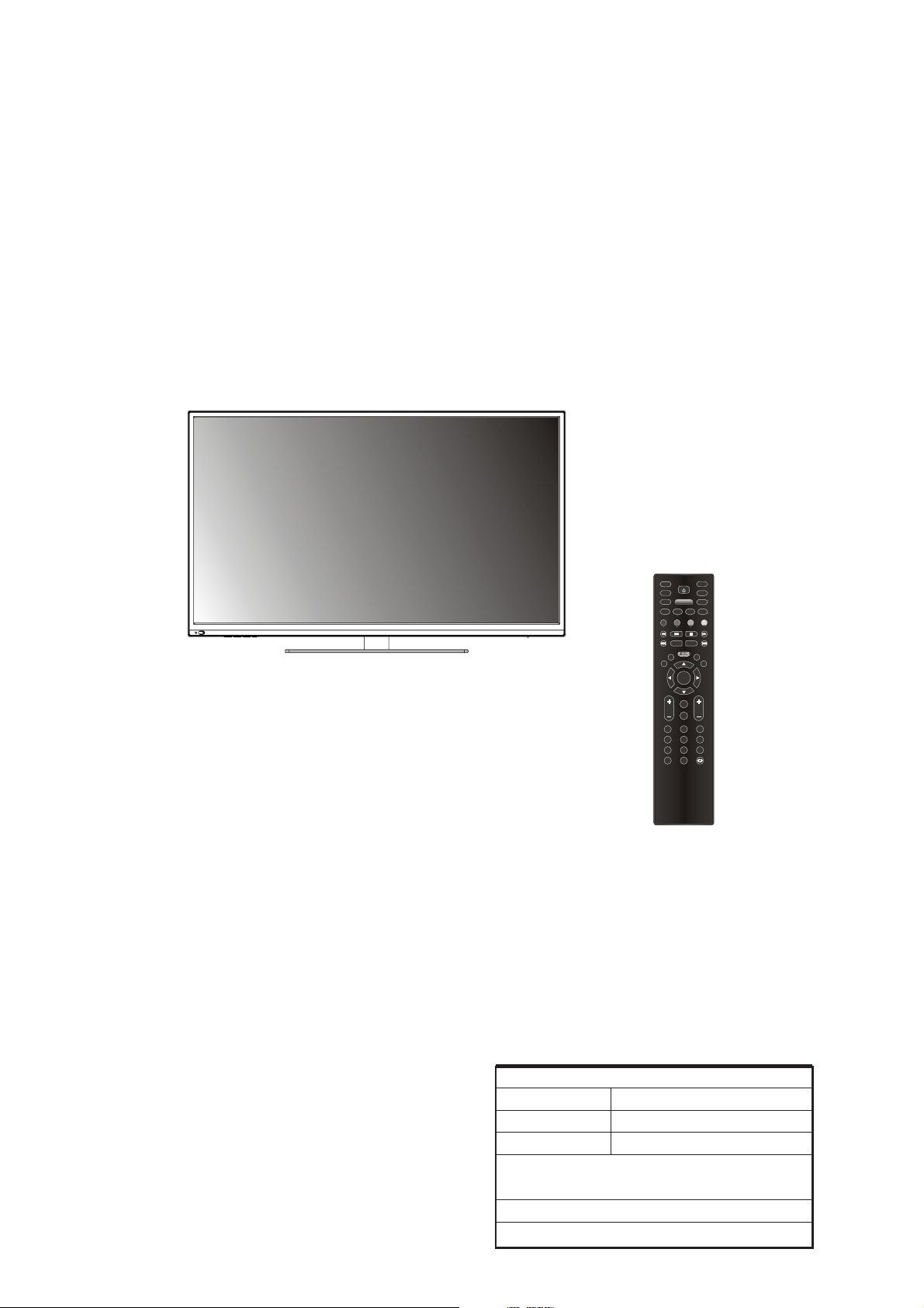
MUTE
FREEZE
POWER
P.P
S.M
SLEEP
ZOOM
HOME
REC CH.LIST FAV EPG
T.SHIFT
INFO
INDEX
SUBTITLE
AUDIO
MTSCC
RETURN
EXIT
OK
MENU
CH
VOL
SOURCE
3
12
6
4
5
789
.
0
Design and specifications are subject to change without prior notice.
(Only Referrence)
SIZE:A5
Description:
MODEL.
JOB NO.
Engineering Dept:
Artwork By:
Checked By:
Approved By:
SERVICE MANUAL 8M51B
Brand Name:
SKYWORTH
Date:
Date:
Date:
2012-5-23
Page 2
Content--------------------------------------------------------------2
11-17
18
19-20
21-28
29-45
46-49
50-57
Page 3

LED 8M51B
Page 4

NTSC-M PAL-M PAL-N
Component
VHF LOW 2~B
VHF HIGH C~W+11
VHF W+12~69
TOSHIBA CODE
55.25MHz ~ 127.25MHz
133.25MHz ~ 311.25MHz
367MHz ~ 801.25MHz
Page 5

65
120
140
For 32” LED
For 42” LED
For 47” LED
Page 6

8
8
6
Page 7
(26inches is 8 ohm)
3.3
3.3
DC Voltage, PANEL(12)
80
12
40
40
3
2
1
4.2
50
0.5
12000
40
3
Page 8
Standard
Standard
20
40
NO
YES
8
6
46
46
NO
Spanish
Page 9

4
2
4
0 40 7 0
0 40 7 0
0 40
40 85
-Y 0 5 0
30000
Page 10
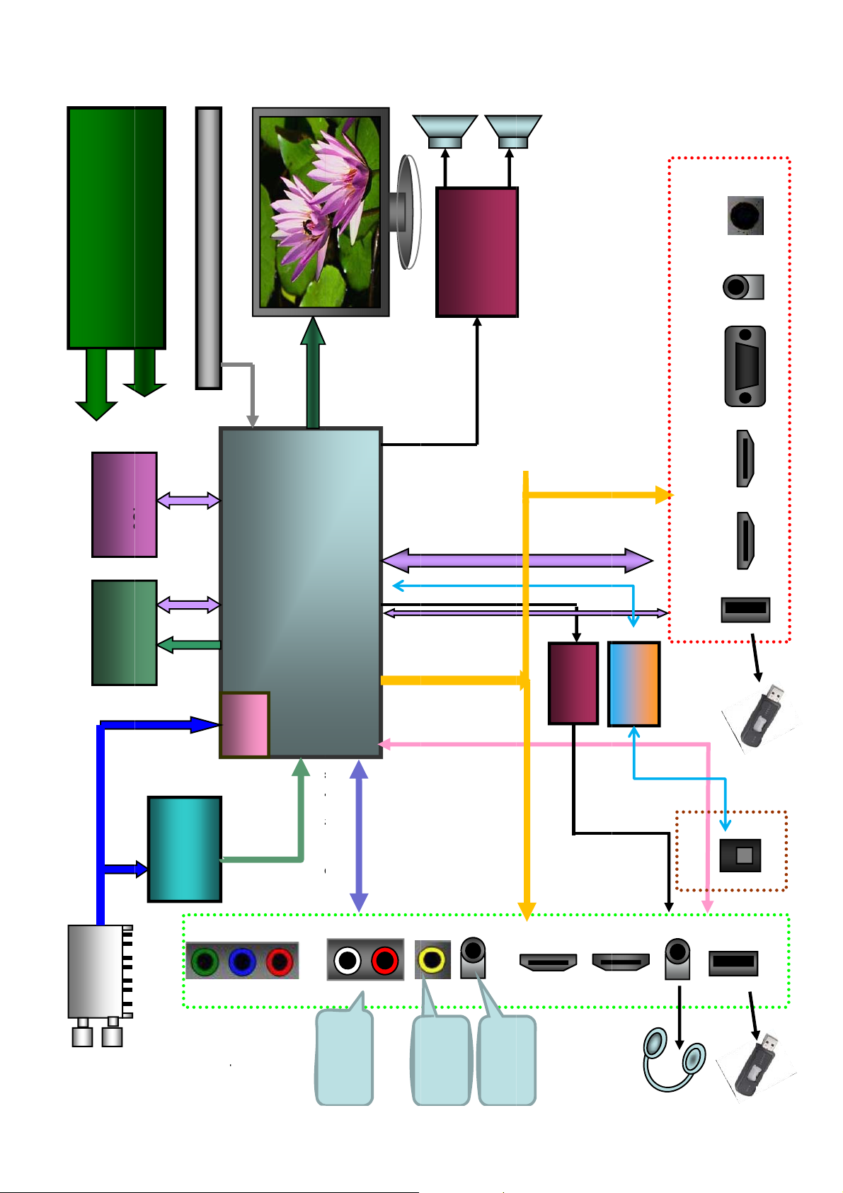
SYSTEM
p
CitAdi
C
it
A
di
Rear Terminal
AMP5707
8W + 8W
KEY PAD, IR Receiver
VGA-Audio
-
FLASH
DDRIII
2Gbx1+1Gbx1
IF+/-
MSD6329
Ultra high speed 32-bi RISC CPU
IF Demo. Build in
MPEG1/2/4 /H.264 Decoder
Analog
Demo
o
u
e +
LED
JPEG MP3 Decoder
PANEL
S
2
I
USB2
USB1
8M51B
.
HP AMP.
BH3544
Transformer
IP101A
R/L
HDMI1
HDMI2
USB2
IF+/-
TC90527
ISDB-T
Demodulator
Block Diagram for 8M51B series
ISDB-T
Analog IF
TUNER
Side Terminal
onent
Com
Serial TS
ompos
L/R
Audio L/R
Composite
HDMI data
Composite
HDMI4
LAN
USB1
HDMI3
Page 11

IC Block Diagram
U2(3.3V/1A 3-TERMINAL POSITIVE VOL TAGEREGULATOR) LD1117-3.3 SOT-223
INPUT
-
Thermal
Shutdown
Ou t
+
-
OUTPUT
GND (Fixed Output)
ADJ (Adjustable Output)
U50 (1.1V/3A LOW DROPOUT LINEARAR REGULATOR)AOZ1051PI SO-8
EN
SS
FB
Reference
& Bias
0.8V
UVLO
& POR
+
EAmp
–
5V LDO
Regulator
Softstart
SS
5μA
Internal
+
PWM
–
Comp
+
+5V
OTP
ILimit
PWM
Control
Logic
Level
Shifter
+
FET
Driver
COMP
500kHz
Oscillator
ISen
VIN
+
–
Q1
LX
Q2
AGND
PGND
Page 12

U3 (2.5V/1A )AS1117L-ADJ A1 SOT-223
Thermal
Shutdown
INPUT
Out
+
-
OUTPUT
GND (Fixed Output)
ADJ (Adjustable Output)
U19 (1.2V/1A)AP1122EG-13 SOT223-3L
Vin
3
Thermal
Shutdown
2 Vout
+
+
CURRENT
LIMIT
1.2V
+
+
GND
1
Page 13

IC Block Diagram
U9(LCDTV CONTROLLER WITH VIDEO ECODE)MSD6329SV-Z1-SVN MSTAR
DVB Digita l T e l evision System -on -Chip
Preliminary PinDiagram /De scrip tion an d Me chan ica l D im ensions Vers ion 0.2
PIN DIAGR AM (M SD 632 9SV)
Top V iew
12345678910111213
A NC LVB0N LVB1P LVBCKN LVB3P LVA 0N LVA 1P LVACKN LVA 3P GN D G ND GN D
B USB0_DM N C N C LVB1N LVB2P LVB3N LVB4P LVA 1N LVA2P LVA3N
C USB0_DP NC NC LVB0P LVB2N LVBCKP LVB4N LVA 0P LVA2N LVACKP LVA 4P
[5 ]
RT C _X OU
GPIO _PM
D NC RTC_XIN
E HW RESET
F SDO
G SD I S C K BIN0P SPD IFO S PD IFI G PIO 198 G PIO 193 GN D GN D G PIO 195 G PIO 183 GN D GN D
H BIN0M SO G IN0 GIN 0P
J GIN 0M R IN0P R IN0M
K B IN1P B IN1M SO G IN1
L GIN 1P GIN 1M R IN1P
M R IN1M B IN2P B IN2M IRIN A V _LINK
N SO G IN2 GIN 2P GIN 2M VSY N C0 H S YN C0 SA R2
GPIO _PM
GPIO _PM
[6 ]/S C Z 1
GPIO 204 GN D GPIO197 GPIO 194 GPIO190 GPIO 202 GPIO 187 LVA4N
T
GPIO 203 GPIO 185 GN D GN D GPIO 199 GPIO189 GPIO 186 GPIO 188
[8 ]
SCZ0 G PIO200 G PIO192 G PIO196 GN D G N D G PIO 191 G PIO201 G PIO 184 GN D GN D
GPIO _PM
GPIO _PM
GPIO _PM
GPIO _PM
[1 0 ]
ET_TX D [1
[1 3 ]
[4 ]
ET_RX D [1]GPIO _PM
[2 ]
ET_R EF_
CLK
]
ET_M DC
ET_TX D [0]ET_TX_E
ET_M D IO
ET_RX D [0]GPIO _PM
[1 ]
GPIO _PM
[3 ]
N
ET_CR S_
DV
[0 ]
GPIO _PM
[1 2 ]
DD CA _D A/
UART0_TX
DD CA _ CK/
UART0_RX
GN D GN D GN D GN D GN D GN D
GN D GN D GN D GN D GN D GN D
GN D GN D GN D GN D GN D GN D
GN D GN D GN D GN D GN D GN D
GN D GN D GN D GN D GN D GN D
GN D GN D GN D GN D GN D GN D
A_DD R3_
A[1]
MSD6329SV
A_DD R3_
A_DD R3_
A_DD R3_
A_DD R3_
A[14]
A[12]
A[11]
A[8]
A_M C LKZ
A_DD R3_
A_DD R3_
A_DD R3_
BA[1]
A[6]
A[4]
P R IN2P R IN2M CV BS5 SA R 0 S AR1 V SY N C1 SA R 3 G N D GN D G N D GN D G N D GN D
R C V B S2 CV BS4 C V B S3 H SY N C1 N C N C PG A_ C OM BY P ASS GN D G N D GN D G N D GN D
NC
IV E
MP LL
[6 ]
[4 ]
[5 ]
AVD D _AU
33
AVD D _EA
R33
GN D G N D GN D
TS1DATA
[1 ]
TS1DATA
[0 ]
TS0DATA
[7 ]
VD D C GN D GN D GN D
GN D GN D GN D
TS 1V A LID T S1 CLK G P IO 137
TS1DATA
[3 ]
TS1DATA
[2 ]
TS1DATA
[4 ]
TS1DATA
TS0VA LID TS0CLK
TS1DATA
[5 ]
[6 ]
TS0DATA
[2 ]
TS1DATA
[7 ]
PCMA D R[1
2]/CI_A[12
]
TS0DATA
[1 ]
TS0DATA
[0 ]
TS0SYNC
C25
NC
AVD D _M
AVD D _AD
AVD D _DV
TS2VALID
K
HOTPLUG
T CV BS1 VCO M CVBS0 AUR0 AU L0
CVBSO UT0CVBSO UT
U
V AU VRM AU VAG AU L2
W AUR2 A U L3 AUR3 G N D GN D G N D N C G N D
Y AUL4 AUR4 AU L1
AA AUR1 AUO UTL1 AUOUTR1
AB AUO UT L0 AUO UTR0
EAR_O UT
AC
R
AD GPIO 180 GPIO 181 GPIO 182
AE G PIO 179 IP VIFM SIFM N C N C
AF IM VIFP SIFP NC NC CEC RXCCKP RXC1N RXC2P RXD0N RXD1P RXBCKN
12345678910111213
XIN XO UT
AUVRP
1
EAR _O UTLDDCDD_CKDDCDB_DADD CD A_C
AVD D _RE
AVD D _DV
DDCDC_CKDDCDC_DADD CD A_DAHOTPLUGBTS0DATA
HOTPLUGCDDCDB_C
DDCDD_
RF_AGC/
F25
I_ U SB
DA
TAGC
AVD D _AD
AVD D _DV
I_ U SB
IF_ A GC A R C0
OD33
C25
I_ U SB
K
D
AVD D _PG
A25
AVD D _AL
NC
AVD D _MPLLAVD D _D
TS2DATA
TS2CLK TS2SYNC TS1SYNC
TS0DATA
RX CC KN RX C 0P RX C 2N RX D C KP RX D 1N RX D 2P RX B 0N
HOTPLUG
TS0DATA
[0 ]
TS0DATA
[3 ]
RX C 0N RX C1P RX D C KN RX D 0P RX D 2N RX B CKP
A
D o c. N o .:20120 10163
Copyright
1/25/2011
2011 M Star Sem icond ucto r, Inc . A llri gh ts re s e rv e d .
Page 14

MSD6329SV
20120 1 0163
DVB Digita l T e l evision System -on -Chip
Preliminary PinDiagram /De scrip tion an d Me chan ica l D im ensions Vers ion 0.2
14 15 16 1 7 18 19 20 21 22 23 24 25 2 6
GN D G N D GN D G N D GN D GN D GN D GN D GN D GN D GN D GN D G N D A
A[10]
A_DD R3_
DQL[5]
A_DD R3_
DQL[7]
A_RASZ A_CA SZ
A_M C LK
A_M CLKE
A_DD R3_
A_O DT A_W EZ
GN D G N D GN D G N D GN D GN D GN D GN D
GN D G N D GN D G N D GN D GN D GN D GN D
GN D G N D GN D G N D GN D GN D GN D GN D
GN D G N D GN D G N D GN D GN D GN D GN D
GN D G N D
GN D G N D GN D
GN D G N D GN D
GN D G N D GN D
GN D G N D GN D G N D GN D GN D GN D GN D
GN D G N D GN D G N D GN D GN D GN D
GN D G N D GN D G N D GN D VD D C GN D GN D
GN D G N D GN D G N D GN D
VDDC VDDC
GN D G N D GN D G N D GN D VD D C A V D D _11
]
NF_AD[1]/P
CMA D R[1]/
CI_A[1]
NF_AD[4]/P
CMA D R[4]/
CI_A[4]
PCMA D R [1
4]/CI_A[14
GPIO 138
NF _ W PZ G PIO 140
PCMA D R [1
1]/CI_A[11
PCMR EG/
CI_CLK
]
RX B 1P RX AC KN RX A 0P RX A 2N
RX B 1N RX B2P RX A0N RX A1P
RX B 0P RX B 2N RX AC KP RX A 1N RX A 2P PC M W EN P C M O EN
14 15 16 1 7 18 19 20 21 22 23 24 25 2 6
A_DD R3_
DQL[1]
A_DD R3_
DQL[3]
AVD D _DDR0AVD D _DDR0AVD D _DDR0AVD D _DD
A_DD R3_
DQU[2]
A_DD R3_
DQML
A_DD R3_
BA[0]
A_DD R3_
A[3]
A_DD R3_
DQU[6]
A_DD R3_
DQU[0]
A_DD R3_
A[5]
A_DD R3_
A[7]
A_DD R3_
DQSBU
A_DD R3_
DQU[4]
A_RESET
A_DD R3_
A[9]
R0
AVD D _DDR0AVD D _DDR1AVD D _DD
R1
AVD D _DDR1AVD D _DD
R1
AVD D _DD
R1
GN D G N D GN D GN D
GN D GN D GN D
DVDD_D
DR
DVDD_D
DR
NF_AD[0]/P
CMA D R[0]/
CI_A[0]
NF_AD[2]/P
CMA D R[2]/
CI_A[2]
NF_AD[7]/P
CMA D R[7]/
CI_A[7]
NF_AD[5]/P
CMA D R[5]/
CI_A[5]
NF_CEZ NF_CEZ1 GN D VD DC N C VD DP VDD P
NF_AD[3]/P
CMA D R[3]/
CI_A[3]
NF_AD[6]/P
CMA D R[6]/
CI_A[6]
GPIO 139
NF _R EZ GN D VD D C VD D C V D D C VD D C PW M2 PW M4 PW M1 AA
NF_RBZ NF_ALE GPIO 40 NC VDDC VDDC PW M3 PW M0 USB1_DP AB
PCMA D R[1
3]/CI_A[13
PCM IRQ/
CI_INT
PCM W AIT
/C I_ W A C
NF _ C LE NF _W EZ G PIO 39
]
PCM IO R/
CI_RD
PCM IO W/
CI_WR
K
A_DD R3_
A_DD R3_
DQSBL
A_DD R3_
A_DD R3_
DQSU
A[13]
DQU[1]
A_DD R3_
DQSL
A_DD R3_
GN D GN D
GN D GN D
BY P ASS_
VCO RE
A[2]
A_DD R3_
DQU[7]
A_DD R3_
DQU[3]
A_DD R3_
A[0]
B_DD R3_
A[14]
B_DD R3_
A[8]
B_DD R3_
A[4]
B_DD R3_
BA[1]
B_DD R3_
A[3]
B_DD R3_
A[7]
B_DD R3_
A[9]
B_DD R3_
A[2]
B_DD R3_
BA[2]
A_DD R3_
DQMU
A_DD R3_
DQU[5]
A_DD R3_
BA[2]
B_M C LKE
B_DD R3_
A[1]
B_DD R3_
A[11]
B_DD R3_
A[6]
B_DD R3_
A[12]
B_DD R3_
A[10]
B_DD R3_
BA[0]
B_DD R3_
A[5]
B_RESET
B_DD R3_
A[13]
B_DD R3_
A[0]
A_DD R3_
DQL[0]
A_DD R3_
DQL[2]
B_DD R3_
DQL[7]
B_DD R3_
DQL[3]
B_DD R3_
DQML
B_DD R3_
DQU[0]
B_DD R3_
DQU[4]
B_DD R3_
DQSBL
B_DD R3_
DQSL
B_DD R3_
DQU[3]
B_DD R3_
DQU[5]
B_DD R3_
DQL[2]
B_DD R3_
DQL[6]
B_ODT B_RASZ GND R
B_ W EZ B_ C A SZ GND T
GN D GN D GN D GN D N C N C
GN D GN D GN D GN D
GPIO 45
PCM CEN/
CI_CS
AVD D _LP
LL
PCMA D R [5]
/CI_A[5]
PCMA D R [0]
/CI_A[0]
GPIO 44/U
ART2_RX
GN D GN D G P IO 102
GPIO 42/U
ART1_TX
PCMA D R [2]
/CI_A[2]
PCMA D R [6]
/CI_A[6]
PCMA D R [1]
/CI_A[1]
GPIO 41/U
ART1_RX
PCMA D R [3]
/CI_A[3]
PCMA D R [4]
/CI_A[4]
CI_RST G P IO 141
I2 S _ O U T
_BCK
I2 S _ I N _ W
S
USB1_DM USB2_DP U SB2_DM AC
PCMA D R [8]
/CI_A[8]
PCMA D R [7]
/CI_A[7]
A_DD R3_
DQL[4]
A_DD R3_
DQL[6]
B_DD R3_
DQL[5]
B_DD R3_
DQL[1]
B_DD R3_
DQU[2]
B_DD R3_
DQU[6]
B_DD R3_
DQSBU
B_DD R3_
B_DD R3_
DQU[1]
B_DD R3_
DQU[7]
B_DD R3_
DQMU
B_DD R3_
DQL[0]
B_DD R3_
DQL[4]
I2 S _ O U T
I2 S _ I N _ SDI2 S _ I N _ B
DQSU
_WS
B_M CLKZ B
B_M CLK C
GND D
GND E
GND F
GND G
GND H
GND J
GND K
GND L
GND M
GND N
GND P
I2 S _ O U T
_SD
I2 S _ O U T
_M CK
CK
DDCR_ CK DDCR_DA Y
PCMA D R [1
0]/CI_A[10
CI_CD
GPIO 43/UA
RT2_TX
]
GPIO 38 AD
PCMA D R [9]
/CI_A[9]
U
V
W
AE
AF
Doc.No.:
Copyright
1/25/2011
2011 M Star Sem icond ucto r, Inc . A llri gh ts re s e rv e d .
Page 15

MSD6329SV
20120 1 0163
DVB Digita l T e l evision System -on-Chip
Preliminary P inDiagram /De scription an d Me chan ical D im ension s Version 0.2
Pin N ame Pin Type Fun ction Pin
G PIO [40:38 ] I/O w / 5V -tolerant G eneralPurpose Input/O utput; 4m A driving strength AB 20,A C21,
AD26
G PIO _P M[ 1 3:12] I/O w / 5V -tolerant G eneralPurpose Input/O utput; 4m A driving strength J4, L7
GPIO_PM[10] I/O w/5V-tolerant G eneralPurpose Input/O utput; 4m A driving strength H 4
G PIO _PM[ 8] I/O w / 5V -tolerant G eneralPurpose Input/O utput; 4m A driving strength E3
G PIO _PM[ 6]/
SCZ1
I/O w / 5 V -t o l erant G eneralPurpose Input/O utput; 4m A driving strength /
ExternalSPI Flash C hipSelect
F2
G PIO _P M[ 5 :0] I/O w / 5V -tolerant G eneralPurpose Input/O utput; 4m A driving strength E2,K4, M 6,L4,
L6, K7
PW M 4 O utput PulseWidth M odulation O utput; 4m A driving strength
AA25
PW M 3 O utput PulseWidth M odulation O utput; 4m A driving strength A B 24
PW M 2 O utput PulseWidth M odulation O utput; 4m A driving strength A A 2 4
PW M 1 O utput PulseWidth M odulation O utput; 4m A driving strength A A 2 6
PW M 0 O utput PulseWidth M odulation O utput; 4m A driving strength A B 25
SAR3 Analog Input SAR Low Speed AD C Input 3;
P7
G eneralPurpose Input/O utput
SAR2 Analog Input SAR Low Speed AD C Input 2;
N6
G eneralPurpose Input/O utput
SAR1 Analog Input SAR Low Speed AD C Input 1;
P5
G eneralPurpose Input/O utput
SAR0 Analog Input SAR Low Speed AD C Input 0;
P4
G eneralPurpose Input/O utput
Doc.No.:
Copyright
1/25/2011
2011 M Star Sem icond ucto r, Inc . A llri gh ts re s e rv e d .
Page 16

DVB Digita l T e l evision System -on-Chip
20120 1 0163
Preliminary P inDiagram /De scription an d Me chan ical D im ension s Version 0.2
DR AM Interfa ce
Pin N ame Pin Type Fun ction Pin
MSD6329SV
A_DD R3_A
[1 4 :0]
O utput D RAM M em ory Address B12,D20,C12,
D 12, D 14,E19,
E12,E18,D 13,
D 18, E13, E 17,
D21,B11,D22
A_DD R3_BA
O utput D R A M M em ory B ank A dd ress D 23, C 13, D 17
[2 :0]
A_M CLKE O utput D R A M M em ory C lock Enable C14
A_O D T I/O Reserved for future O n-D ieTermination E15
A_W EZ O utpu t W rite Enable; active low E16
A_R ASZ O utput Row Address Strobe; active low D 15
A_CASZ O utput Column Add re ss Strobe; active low D 16
A_M CLK O utput D RAM M em ory Positiv e D iffe re n t i alClock B1 4
A_M CLKZ Output DRAM M em ory Negative D ifferentialClock B13
A_DD R3_D Q MU O utput D ata M ask forLow Byte; active high B23
A_DD R3_D Q ML O utput D ata M ask forLow Byte; active high C17
A_DD R3_D Q SU I/O D ata Strobe B20
A_DD R3_D Q SL I/O Data Strobe C 21
A_DD R3_D Q SBU I/O D ata Strobe Inverse B19
A_DD R3_D Q SBL I/O D ata Strobe Inverse C 20
A_DD R3_D QU
[7 :0]
I/O D RAM M em ory D ata Bus B22,B18,C23,
C19,C22,B17,
B21, C18
A_DD R3_D QL
[7 :0]
I/O D R A M M e m o ry D a ta B u s C 1 5 , C 2 5 , B 1 5 ,
B25, C16,C 24,
B16, B24
A_R ESET Input D R A M M em ory R eset; active low D 19
B_D DR 3_A
[1 4 :0]
O utput D RA M M em ory Address G 22, R2 3,K23,
H 23, L23, P22,
H22,N22,J23,
N23,J22,M 22,
R22,G 23,T23
B_D DR 3_BA
O utput D R A M M em ory B ank A ddress T 22,K 22,M 23
[2 :0]
B_M CLKE O utput D R A M M em ory C lock Enable E23
B_O D T I/O Reserved for future O n-D ieTermination R 24
Doc.No.:
Copyright
1/25/2011
2011 M Star Sem icond ucto r, Inc . A llri gh ts re s e rv e d .
Page 17

DVB Digita l T e l evision System -on-Chip
20120 1 0163
Preliminary P inDiagram /De scription an d Me chan ical D im ension s Version 0.2
Pin N ame Pin Type Fun ction Pin
B_W EZ O utput W rite Enable; active low T24
B_R ASZ O utput R ow Address Strobe; active low R 25
B_CASZ O utput Column Address Strobe; active low T25
B_M CLK Output D RAM M em ory Positiv e D ifferen tialClock C26
B_ M CLK Z O utput D R A M M em ory N egative D ifferential C lock B 26
B_D D R 3_D Q MU O utput D ata M ask for Low Byte; active h igh M 25
B_DDR3_DQML Output Data Mask forLow Byte;active high F24
B_DDR3_DQSU I/O Data Strobe J25
B_DDR3_DQSL I/O Data Strobe K24
B_DDR3_DQSBU I/O Data Strobe Inverse H 25
B_DDR3_DQSBL I/O Data Strobe Inverse J24
MSD6329SV
B_D DR 3_DQU
[7 :0]
I/O D R A M M em ory D ata B u s L25, G 2 5, M 24,
H 24 , L24, F25,
K25, G 24
B_D DR 3_DQL
[7 :0]
I/O D RA M M em ory D ata Bus D 24, P24,D 25,
P25,E24,N 24,
E25,N 25
B_ RE SET In put D R A M M em ory R eset; active low P23
Ethernet RM IIInterface
Pin N ame Pin Type Fun ction Pin
ET_CR S_D V I/O w / 5V-tolerant Eth ernet M AC Ca rrier Sense/R eceive D ata Valid J7
ET_TXD [1:0] O utput w / 5V -toleran t E thernet M A C T ran sm itD ata B u s J5 ,H6
ET_TX_EN O utput w / 5V -toleran t E thernet M A C T ran sm itEnable H7
ET _R EF_C LK Input w / 5V-tolerant Ethernet M AC Synchronous C lock R eferen ce for R eceive,
Transm itand ControlInterface
ET_R XD [1:0] Input w / 5V-toleran t E th ern et M AC R eceive Da ta Bus L5, K6
ET_M D C O utput w / 5V-toleran t E thernet M A C M anagem en t Da ta Clock K5
ET_M D IO I/O w / 5V-tolerant Ethernet M AC M anagem entD ata Bus J6
H5
Doc.No.:
Copyright
1/25/2011
2011 M Star Sem icond ucto r, Inc . A llri gh ts re s e rv e d .
Page 18

MSD6329SV
20120 1 0163
DVB Digita l T e l evision System -on-Chip
Preliminary P inDiagram /De scription an d Me chan ical D im ension s Version 0.2
USB Interface
Pin N ame Pin Type Fun ction Pin
USB0_DP Analog I/O U SB N on Inverting D ata Input/O utputfor Port0 C1
USB0_DM Analog I/O U SB In verting Da ta Input/O utput for Port 0 B1
USB1_DP Analog I/O U SB N on Inverting D ata Input/O utputfor Port1 AB26
USB1_DM Analog I/O U SB In verting Da ta Input/O utput for Port 1 AC 24
USB2_DP Analog I/O U SB N on Inverting D ata Input/O utputfor Port2 AC25
USB2_DM Analog I/O U SB In verting Da ta Input/O utput for Port 2 AC 26
UART Interface
Pin N ame Pin Type Fun ction Pin
GPIO44/
U ART2_RX
GPIO43/
U ART2_TX
GPIO42/
U ART1_TX
GPIO41/
U ART1_RX
D D CA _DA/
U ART0_TX
DDCA_CK/
U ART0_RX
I/O w / 5 V -t o l erant G eneralPurpose Input/O utput; 4m A driving strength /
UniversalAsynchronous R eceiver 2
I/O w / 5 V -t o l erant G eneralPurpose Input/O utput; 4m A driving strength /
UniversalAsynchronous Transm itte r 2
I/O w / 5 V -t o l erant
G eneralPurpose Input/O utput; 4m A driving strength /
UniversalAsynchronous T ransm itte r 1
I/O w / 5 V -t o l erant
G eneralPurpose Input/O utput; 4m A driving strength /
UniversalAsynchron ous R eceiver 1
I/O w / 5 V -t o l erant DDC D ata for A n alog port /
UniversalAsynchronous T ransm itte r 0
I/O w / 5 V -t o l eran t DDC C lock for A n alog port /
UniversalAsynchron ous R eceiver 0
AF21
AF25
AC22
AC23
M7
N7
VIF Interface
Pin N ame Pin Type Fun ction Pin
VIFM Analog Input N egative Video IF Input AE3
VIFP Analog Input P ositive Video IF Input AF3
RF_AGC/
TAGC
Analog O utput R F A G C /
Tun erA utom aticG ainControlO utput
AD4
PGA_CO M Analog Input V IF PG A N egative Source R7
Doc.No.:
Copyright
2011 M Star Sem icond ucto r, Inc . A llri gh ts re s e rv e d .
1/25/2011
Page 19

MSD6329SV
20120 1 0163
DVB Digita l T e l evision System -on-Chip
Preliminary P inDiagram /De scription an d Me chan ical D im ension s Version 0.2
Misc.Inter face
Pin N ame Pin Type Fun ction Pin
D D CA _DA/
U ART0_TX
DDCA_CK/
U ART0_RX
I/O w / 5 V -tol era nt D DC Da ta for A nalog p ort /
UniversalAsynchronous Transm itte r 0
I/O w / 5 V -tol erant DDC Clock for A n alog port /
UniversalAsynchronous Receiver 0
M7
N7
D D CDA _DA I/O w / 5V -tolerant H DC P SerialBus Data /DDC Data ofDVI/HDMIPortA Y6
D D CDA _CK Input w / 5V -toleran t HDC P SerialBus C lock / D D C ClockofDVI/HDMIPortA AB6
DDCDB_DA I/O w/5V-tolerant H DC P SerialBu s D ata / D D C Da ta of D VI/HD M I Port B A B5
DDCDB_CK Inputw/5V-tolerant H DC P S erialBu s C lock / D D C C lockofDVI/HDMIPortB AA5
D D CDC _DA I/O w / 5V -tolerant H DC P SerialBu s D ata / D D C Da ta of D VI/HD M I Port C Y5
D D CDC _CK Input w / 5V -toleran t HDC P SerialBus C lock / D D C ClockofDVI/HDMIPortC Y4
D D CDD _DA I/O w / 5V-tolerant H DC P SerialB us D ata / D D C Da ta o f D VI/H D M I P o rt D AC 4
D D CDD _CK Input w / 5V-tolerant H DC P S erialBus C lock / D D C C lockofDVI/HDMIPortD AB4
HOTPLUGA I/O w/5V-tolerant H ot-plug controlforDVI/HDMIPortA AE7
H O T PLU GB I/O w / 5V -tolerant H ot-plug controlfo r D VI/H D M I Po rt B Y7
HOTPLUGC I/O w/5V-tolerant H ot-plug controlforDVI/HDMIPortC AA4
HOTPLUGD I/O w/5V-tolerant H ot-plug controlforDVI/HDMIPortD AD6
D D C R _DA I/O w / 5V -toleran t D DC Da ta fo r R O M Y 26
D D C R _C K I/O w / 5V-tolerant D DC Clock for RO M Y25
XIN C rystalO scillator Inpu t CrystalO scillator Inpu t A C2
XO UT C rystalO scillator O utput C rystalO scillator O utput A C3
RTC_XOU T CrystalOscillator O u tput R TC 32KH z CrystalO utput D3
RTC_XIN CrystalOscillator Input RT C 32K H z C rystalInp ut D2
IR IN Input w / 5V-tolerant IR R eceiverInput M4
H W R ESET Schm ittTriggerInput w /
Hardware Reset;active high E1
5V-tolerant
BYP A SS For ExternalBypass Capacito r R 8
IF_AG C O utput w / 5V -tolerant IF AG C A C5
RF_AGC/
TAGC
O utput w / 5V -tolerant R F A G C /
Tun erA utom aticG ainControlO u tpu t
AD4
CEC I/O Consum er ElectronicsControl AF7
AV_LINK
BYP ASS_VCO RE
I/O
Output
AV Link
In tern al VCO R E Volta g e T e st ing Point
M5
R21
Doc.No.:
Copyright
1/25/2011
2011 M Star Sem icond ucto r, Inc . A llri gh ts re s e rv e d .
Page 20

DVB Digita l T e l evision System -on-Chip
20120 1 0163
Preliminary P inDiagram /De scription an d Me chan ical D im ension s Version 0.2
Pow er Pins
Pin N ame Pin Type Fun ction Pin
AVDD _LP LL 3 .3V P ow er LPLL P ow er W 21
A V DD _D M PLL 3.3V P ow er CrystalPow er V8
A V DD _M PLL 3.3V Pow er M PLL Pow er V7
AVDD _ALIVE 3.3V Pow er Alive D om ainIO Power U8
AV DD _D VI_U SB 3.3V Pow er D VI U SB Pow er V4-V6
AV DD _EAR 33 3.3V Pow er Earphone D river Pow er U 9
A V DD _A U 33 3.3V P ow er Audio Pow er T9
AV DD _AD C25 2.5V Pow er V ideo AD C Pow er U 5, U6
AV DD _REF25 2.5V Pow er D em od AD C Pow er U 4
AV DD _M O D 33 3.3V Pow er M O D 3.3V Pow er T6
AV DD _PG A25 2.5V Pow er Dem od PG A Pow er T 7
AVDD _11 1.1V Pow er A nalog 1.1V Pow er W 20
AVDD _DD R0 1.5V Pow er D D R3 Pow er K1 6-K19,L17
MSD6329SV
AVDD _DD R1 1.5V Pow er D D R3 Pow er L18, L19,M 17,M 18,N 17
D V DD _DDR 1.1V Pow er D D R 1.1V Pow er U19,V 19
VD DP 3.3V Pow er D igitalInput/O utput Pow er Y22,Y 23
VDDC 1.1V Pow er D igitalCore Pow er T10,T 19,V14, V16,W 19,Y20,
AA20-AA23,AB22,AB23
G ND G round Ground A11-A 26,D 5,D 26, E6,E7,E26,F7,
F8, F12-F21, F26, G 8, G 9, G 12-G 2 1,
G26,H8-H21,H26,J8-J21,J26,
K8-K15,K 20,K21,K26, L8-L16,L20,
L21 , L26, M 8-M 16 , M 19-M 21, M 26,
N 8-N 16,N 18-N 21, N 26,P8-P21,P2
R 9-R 20, R 2 6, T11-T18,T 2 0, T 21,
T26,U10,U12-U18,U20-U23,
V 9 -V 1 1 , V 2 0 -V 2 3 , W 9 - W 1 1 ,
W 13-W 18,W 22,W 23,Y19,AA 19
No Connects
Pin N ame Pin Type Fun ction Pin
NC No conn ect A2,B2,B3,C2,C3,D 1,R5,R6,T8,
U 7,U24,U 25,W 12,Y21,AB21,
A E5, AE6, AF 5, A F6
AD5 ,
6,
Doc.No.:
Copyright
1/25/2011
2011 M Star Sem icond ucto r, Inc . A llri gh ts re s e rv e d .
Page 21

IC Block Diagram
U1(DUAL BTLCLASS D AUDIO AMPLIFIER) TAS5707
SDIN
MCLK
SCLK
LRCLK
SDA
SCL
Serial
Audio
Port
Sample Rate
Autodetect
and PLL
Serial
Control
Terminal Control
L
7BQ
R
7BQ
Microcontroller
Based
System
Control
mDAP
V
O
L
U
M
E
DRC
Click and Pop
Control
S
R
C
th
4
Order
Noise
Shaper
and
PWM
2HB´
FET Out
2HB´
FET Out
Protection
Logic
OUT_A
OUT_B
OUT_C
OUT_D
Page 22

U4 ˄1.5V/5A˅AS1084R/TRͲLFADJUSTABLETOͲ252
U52 ǃU59˄5V/2A˅MP1494DJͲLFͲZTSOTͲ23Ͳ8
U18 ˄3.3V/5A˅AS1084RͲ3.3/TRͲLFTOͲ252
Page 23

Page 24

U1664MX16BITGͲDIEDDR3Ͳ1333SDRAMFBGAͲ96
Page 25

U17128MX16BITGͲDIEDDR3Ͳ1333SDRAMFBGAͲ96
Page 26

U816MBSPIFLASHSOPͲ8
U212GBITCMOSNANDEEPROMTSOPI48
Page 27

Page 28

Main PCB Top/Bottom Layer
Page 29

Main PCB Top/Bottom Layer
Page 30

8M51B
Service Adjustment
(V0. 1)
Page 31

1. How to enter and exit factory mode
Press Source button, and then press digital button “3”, “1”, “9”, “5” in turns to enter the factory menu. Press ©
and ª button to choose the item
In the factory mode, press “menu” key can exit the factory mode.
Software information:
Enter factory mode, you can get the software information from the bottom of menu.
ˈpress OK button to enter the submenu and press ¨ button to adjust the value.
Panel information:
Enter factory mode, enter “PANEL CONTROL” item, you can get the panel information from the bottom of
menu.
Aging mode
Enter factory mode, select “SYSTEM SETTING” item, press OK button enter, select “AGING MODE” item,
press ¨ button open aging mode.
Note: You can press the shortcut key in the factory remote control to open or close the aging mode.
4. How to adjust ADC
Before adjusting, enter the channel you want to adjust and input adjust signal (YPBPR channel: 576P and 720P,
100% color bar; VGA channel: 1366*768, tessellated white and black). Select “AUTO ADC”, press¨button to
auto adjusts the ADC value.
100% color bar
Page 32

Tessellated white and black
Note: 1. The YPBPR and VGA’s Auto White Balance adjust (AUTO ADC) must be done on the product line.
2. In YPBPR channel, must adjust the SD and HD two modes.
5. How to adjust White Balance
Enter factory mode, select W/B ADJUST and go to the “MODE” item to select the channel which you want to
adjust then select the color temperature (Medium, Warm, Favorite and Cool). Then press ª Key to go to these
items you want to adjust:
R Gain
G Gain
B Gain
R Offset
G Offset
B Offset
Press § or ¨ key can adjust the value to the best effect.
COPY ALL: Copy there values to all source!
6. How to update MBoot
MBoot: The boot software, which is stored in the SPI flash.
(1) Open MSTAR ISP Utility tool.
Page 33

(2) Connect the debug tool to the device, turn on TV. Press “Connect” button.
(3) Press “Read” button to choose the MBoot file.
Page 34

(4) Press “Auto” button, set parameter.
(5) Press “Run” button to begin program.
(6) If program success, it will show “Pass” message, otherwise, you need to reconnect and try again.
Page 35

7. How to update main software (by USB):
˖
˖
(1) Copy the new software (name by “MstarUpgrade.bin”) to the root directory of USB drive.
(2) Plug the drive to the USB socket.
(3) Enter factory, select “Software Update (USB)” item and press OK button to begin update.
(4) TV set will restart when finish.
Note:
(1) You need to do “Restore Default” in the factory mode after software update.
(2) You need to restart the TV set again by AC power.
8. HDCP key and MAC address burning
(1) Turn on TV and insert the bus wire of burning tool to main board of CON32.
(2) Enter into factory mode then set the “I2C BUS” to off.
(3) Put the code bar spear on the code bar then press the switch to begin burning.
(4) After burning, set the “I2C BUS” to on.
9. ESN master(24C08 E2PROM)
Note: 8M51B use the 24C04 on the board.
Page 36

ADC ADJUST MODE
NIAG-R
NIAG-G
NIAG-B
TESFFO-R
TESFFO-G
TESFFO-B
CDAOTUA
W/B ADJUST MODE
looC/mraW/muideMERUTAREPMET
NIAG-R
NIAG-G
NIAG-B
TESFFO-R
TESFFO-G
TESFFO-B
LLAYPOC
Panel control TI Mode On/Off On/Off : adjust the TI mode of LVDS
hctiwslennahcneve-ddoffO/nOSDVL
)tib03(01/)tib42(8retemaraPffO/nOtroP
ecrruoSputratSNACSREVO
porCthgiR
porCpU
porCnwoD
SYSTEM SETTING Fac.Hotkey On/Off Factory hot key enable
ffO/nOedoMgnigA
OSD Language English On/Off
ffO/nOHCNERF
ffO/nOESEUGUTROP
ffO/nOHSINAPS
Input Sourrce AV1 On/Off
ffO/nO2VA
ffO/nO1IMDH
ffO/nO2IMDH
ffO/nO3IMDH
ffO/nO4IMDH
ffO/nO1VUY
ffO/nO2VUY
ffO/nOBGR-CP
Top/Bottom/Left/Right
HCNERF/ESEUGUTROP/HSINAPS/hsilgnEegaugnaLtluafeD
elihC/ureP/anitnegrA/lizarByrtnuoC
/nOrewoP/yromeM/ybdnatSedoMnOrewoP
gnikrowlamron-no,neposub-ffOffO/nOSUBC2I
latesertluafeDerotseR l value to factory default
tluafedotlennahcteserslennahcteserP
ehtfoezisehttsujdanacsmetiesehTporCtfeL
Page 37

Analog Curve Mode
BRIGHTNESS
CONTRAST
SATURATION
HUE
SHARPNESS
VOLUME
PICTURE MODE Startup Source
MODE Natural/Cinema/Favorite/Game/Dynamic
BRIGHTNESS
CONTRAST
COLOR
SHARPNESS
TINT
Mac Address Update
HDCP Key Update
CI PLUS Key UPDATE No use
SOFTWARE UPDATE(USB)
SW INFORMATION
SSC SETTING
VIF INITIALIZATION
PIP/POP PIP/POP
PIP Border Width
3D 3D
3D Output Mode
CUSTOMER SETTING
WHITE PATTERN
WDT
PVR RECORD ALL
UART ENABLE
CI+Credential Mode No use
Power on LOGO Select the logo
Stagecraft 1.2 certification
Audio Hidev Mode No use
Others
Netflix Key Update
2Q2II
2Q2II
2Q2II
2Q2II
2Q2II
Tes t pat t ern
Watch dog
Off- close the UART debug. On- open
Page 38

External Schematic and Connections
Note: The graphics are for representation only.
Front view
3
21
5 4 367
1
Power indicator / Remote sensor
2
Speakers
3
Standby Button
4
Source Button
5
Menu Button
6
Volume Down/Up Button
7
Channel Down/Up Button
1
2
Page 39

External Schematic and Connections
Note: The graphics are for representation only.
Back view
Side and Rear AV terminals view
1
LAN
2
USB1/2
3
HDMI1/2/3/4
4
PC-RGB input
5
PC-RGB audio input
6
RF input
7
YPbPr input
8
AV input
9
Earphone output
10
S/PDIF output
LAN IN
USB1
5V 500mA
HDMI1
1 2 3 4 5 6
HDMI IN
HDMI2
PC-RGB
IN
PC-RGB
AUDIO IN
CABLE AIR
RF IN
Y
b
7
P
YPbPrIN
r
P
LEFT
8
AV IN
VIDEO RIGHT
HDMI4
3
HDMIIN
HDMI3
9
2
USB2
5V 500mA
S/PDIF
10
Page 40

Remote Control Descriptions
13
1
POWER
MUTE
ZOOM
FAV EPG
3
S.M
5
7
8
10
12
FREEZE
2
SLEEP
REC
P.P
HOME
CH.LIST
4
6
9
11
T.S HIF T
1. Standby( )
Press to turn the TV on or off(standby).
2. Freeze
Press to freeze or unfreeze the picture.
Note: This button is in USB channel.useless
3. Mute
Press to mute or restore the volume.
4. Picture Mode( P.P )
Press to select the desired picture
mode.
INFO
EXIT
SUBTITLE
CC
INDEX
AUDIO
MTS
RETURN
5. Sound Mode( S.M )
Press to select the desired sound mode.
6. Sleep
Press to set the time to switch the TV to
standby mode.
OK
7. Zoom
Press to select the desired picture aspect ratio.
8. Home
MENU
VOL
SOURCE
12
4
5
7
89
.
0
CH
3
6
Enter the home .desktop
9. Record(REC)
Press to record the current DTV program.
10. EPG
Press to display the EPG information in DTV
program.
11. Channel List(CH LIST)
Press to display the available channel list.
12. Favorite Channel(FAV)
Press to view your assigned favorite channels.
Press Up/Down buttons to cycle through your
assigned favorite channels, press OK to confirm.
13.Color buttons
Press to execute the prompt function.
Page 41

14
15
17
19
FREEZE
POWER
P.P
SLEEP
HOME
CH.LIST
REC
T.S HIF T
INDEX
SUBTITLE
CC
EXIT
OK
MENU
VOL
SOURCE
12
4
5
7
89
.
0
Remote Control Descriptions
14. ButtonsControl
MUTE
S.M
ZOOM
FAV EP G
INFO
AUDIO
MTS
CH
3
6
RETURN
16
18
20
Fast Backward ( )
Press to fast reverse.
Fast Forward ( )
Press to fast forward.
Previous ( )
Press to play the previous file.
Next ( )
Press to play the next file.
Play & Pause ( )
Press to pause playback,
press again to continue playback.
Stop ( )
Press to stop the playing.
15. Index
Press to view the PVR files list in AIR source.
16. INFO
Press to display relevant information such as
screen format, source, etc.
17. Closed Caption(CC)
Press to turn switch the mode of Closed Caption.
Subtitle
Press to open or close the video subtitle in
USB status.
18. MTS
Press to select desired sound output(Mono,
Stereo or SAP)depending on the broadcasting
channel.
AUDIO
Switch audio channel if there is a multichannel
program.
19. Exit
Press to exit from any menu.
20. Return
Return to previous menu in Ginga mode.
Page 42

Remote Control Descriptions
POWER
HOME
OK
MENU
SOURCE
5
0
MUTE
S.M
ZOOM
FAV EP G
INFO
AUDIO
MTS
CH
3
6
21
RETURN
23
26
25
27
FREEZE
P.P
SLEEP
CH.LIST
REC
T.S HIF T
INDEX
SUBTITLE
CC
EXIT
22
24
VOL
12
28
4
789
29 30
.
21. NETFLIX
Connect to Netflix.
22. Up/Down/Left/Right Cursor
( / / / )
Press to the desired item
select and adjust
on the menu.
Note: In USB mode, press " " can show
the control menu, press " " can hide the
control menu.
23. OK
Press to confirm and execute the selection.
24. Volume Up/Down (VOL+/-)
Press to adjust the volume.
25. Channel
Press to select channel.
Up/Down (CH+/- )
Next/Previous
26. Menu
Press to enter or exit from the TV menu.
27. Source
Press to select the input source mode.
Note:It is no work in the net application or USB.
28. Program Select (0-9)
Press to select the TV channel directly.
29.
Press to select the digital sub program.
30.
Press to review the last program.
Page 43

Welcome setting & Home
Initial setup
The first time you power on the TV, there will show a setup wizard, please follow the wizard:
Step 1.Select the language you need.
Step 2.Select the time zone of you place. (Note 1)
Step 3.Select the picture mode you like.
Step 4.Select the tuner mode. Press "OK" to scan the program.
Home
Presses "HOME" enter the home menu. There are some shortcuts in the desktop:
SETTING - Change the TV setting, including:
Advanced Option:
Menu Language - Change the menu language
Time Zone - Change the time zone of you place. (Note 1)
DivX Registration - Register TV set to play DivX video. (Note 1)
DivX Deactivation - Deactivate DivX. (Note 1)
Netflix Registration - Register Netflix. (Note 1)
Netflix Deactivation - Deactivate Netflix. (Note 1)
Network Setting: Change the setting of wire and wireless net.
Info: Show the information about the TV set.
SOURCE - Open the source list, select and switch the TV source.
DLNA - Begin the Digital Living Network Alliance application. (Note 1)
VIDEO - Enter the USB state, play the video file.
MUSIC - Enter the USB state, play the music file.
PHOTO - Enter the USB state, view the photo file.
FILE - Enter the USB state, view the text file.
Netflix - Begin the Netflix application, connect to Netflix. (Note 1)
Facebook - Begin the Facebook application, connect to Facebook. (Note 1)
Picasa - Begin the Picasa application, connect to Picasa. (Note 1)
Youtube - Begin the Youtube application, connect to Youtube. (Note 1)
Terratv - Begin the Terratv application, connect to Terratv.(Note 1)
Twitter - Begin the Twitter application, connect to Twitter.(Note 1)
Web Browser - Open the web browser.
(Note 2)
Note 1, Option item, no visibility to some TV set.
Note 2, Web Browser only supports the HTML5 video file format.
Netflix
Facebook
AIR
SETTING SOURCE DLNA VIDEO MUSIC PHOTO FILE
Youtu be Terratv
WebBr owser
Picasa
Twitter
Page 44

Welcome setting & Home
Network setting
Wi-Fi Network
Plug a Wi-Fi dongle to the USB socket.
Press "HOME" key enters the home page.
Select SETTING item, press "OK"key to open the SETTING page.
Select "Network Setting" item, press "OK" key to open the page.
Press " " key to select "Wi-Fi Network" item.
Press " " key to select "Wi-Fi Switch" item.
Press " " key to select on, press "OK" to confirm setting.
Press "MENU" exits "Wi-Fi Switch" item.
Press " " key to select "Station" item.
Press " " key to select your base station, press "OK" to enter connection page.
If the base station need password, select "Password" item, press "OK" to input the
password.
Press blue color key to connect the base station.
Notes:
Please use the Wi-Fi dongle which is equipped with the TV set. No all Wi-Fi dongle is
supported.
Not guarantee that all can use the keyboard and mouse more varieties.
Wired Network
Plug the network wire to the LAN socket.
Press "HOME" enters the home page.
Press " " key to select SETTING item then press "OK" to open the SETTING page.
Press " " key to select "Network Setting", press "OK" to open the page.
Press " " key to select "Configuration" item, press " " enters into the page.
Select "Connect" item, press "OK" to test the status.
Page 45

PVR & Time Shift
PVR
Press "REC" key to record.
Press [ ] key to exit record.
Press [ ] key to play or pause the recording program.
Press [ ] / [ ] key to display or hide the control menu.
Press button to Press button
[INDEX] display the list of recorded programs. OK to play.
Press red button to note
can jump directly to the end of the segment play.
Press button to
green show or hide the camera picture. select any pictures, you can play
the beginning of the period of time in the picture. OK to play as a starting
point in this picture when elected in the picture.
Press button to
yellow remove the camera pictures.
Press button to
blue take the current screen.
Pre ss [ ] / [ ]
button to fast rewind or fast forward when the cursor to above the playback
progress bar.
Notes:
PVR only works with the digital signal program.
Before you recording, please make sure that the USB disk has enough free memory.
Please use a high speed USB device.
The file can be played in the AIR or USB source, can't be played in other player,
including PC.
This TV can only support the FAT16, FAT32 format USB device.
The recorded files can only be played in this TV, does not ensure normal playback in
other TV.
the initial segment and end segment, when the replay, you
Press button
T-SHIFT
00:00 03:38
80
Time Shift
Press "T.SHIFT" key to begin time shift.
Press [ ] key to exit time shift.
Press [ ] key to play or pause the time shift.
Press [ ] / [ ] key to display or hide the control menu.
Notes:
Time shift only works with the digital signal program.
Before you start time shift, please make sure that the USB disk has enough free
memory.
Please use a high speed USB device.
Page 46

MENU setting
Menu Operation
Press "MENU" key to enter the main menu .
Press the[ ] / [ ] guide key to select desired item.
Press "OK" key to enter the item.
Press "MENU" key to exit the item.
Picture
Picture Mode Cine ma
Color Temperature
Picture Size
Noise Reduction
MPEG Noise Reduction
Dynamic Contrast
Film Mode
PICTURE
Picture Mode: Contain "Natural", "Cinema", "Favorite", "Game" and "Dynamic".
("Game" mode is no useful at the AIR, CABLE and USB source.)
Color Temperature: Contain "Normal", "Warm", "Favorite" and "Cool".
Picture Size: Contain "Auto", "4:3", "16:9", "ZOOM1", "ZOOM2", "Panoramic" and
"Just Scan". (Some option is no visible at some source.)
Noise Reduction: Contain "Off", "Low", "Middle" and "High" four modes .
(No useful at PC-RGB source)
MPEG Noise Reduction: it contain "Off", "Low", "Middle", "High".
(No useful at PC-RGB source)
Dynamic Contrast: Contain On and Off. (No useful at PC-RGB source.)
Film Mode: Contain On and Off. (No useful at PC-RGB source.)
RGB Mode Setup: Contain the follow option.
Auto Adjust: Adjust the screen automatically.
H Position: Adjust the horizontal position.
V Position: Adjust the vertical position.
Clock Phase: Adjust phase.
H Clock: Adjust the synchronous clock.
Page 47

MENU setting
Audio
Sound Mode Standard
Balance
surround sound
PerfectVolume
DigitalAudio Output
Audio Delay
AUDIO
Sound Mode: Contain "Standard", "Music", "Movie", "Speech" and "Favorite".
Balance: Control the sound balance between the right and left loudspeaker (earphone).
Surround Sound: Contain On and Off.
Perfect Volume: Contain On and Off. Adjust the volume corresponding to the input
audio level.
Digital Audio Output: Contain AUTO and PCM
Audio Delay: Adjust the speaker delay time to synchronize with video
(Only Useful at DTV source).
Time
Auto Sync Off
00:00
Clock
Power Off Time
Power On Time
Sleep Timer
Auto Sleep
TIME
Auto Sync: Can set TV time synchronize with the system or not. It is working when
you receive DTV signal.
Clock: Set the time of TV set by manually when the "Auto sync" is set to "Off".
Power Off Time: Set the time of TV set auto standby.
Power On Time: Set the time of TV set auto power on.
Sleep Timer: Contain off, 10, 20,30,60,90,120,180,240 minutes.
Auto Sleep: TV set auto to standby when there is no signal. Contain On and Off.
Page 48

MENU setting
Setup
Auto Tnuing
DTV ManualTuning
TV ManualTuning
ChannelEdit
Signal Information
SETUP
Auto Tuning: Search and save all programs at current source by automatically.
DTV Manual Tuning: Search and save the digital programs at AIR source by manually.
TV Manual Tuning: Search and save the analog programs at current source by manually.
Channel Edit: Edit the programs. You can skip the programs or add the programs in the
favorite list.
Signal Information: Showing the information of current DTV channel.
Function
Audio Language English
Subtitle
PVR File System
Closed Caption
HDMICEC
DTVisetup
Restore Factory Default
FUNCTION
Audio Language: Set the primary or secondary digital audio language corresponding
to the signal.
Subtitle: Contain On and Off.
PVR File System: Personal Video Record setting. If you want to use this function, you
must receive a digital program and plug a USB disk.
Closed Caption: Analog closed caption, contain CC1, CC2, CC3, CC4, TT1, TT2, TT3
and TT4.
HDMI CEC: HDMI linking setting.
DTVi Setup: Ginga switch, contain On and Off.
Restore Factory Default: Restore user setting to the default.
Page 49

MENU setting
Lock
Lock System Off
SetPassword
Block Program
Parental Guidance
LOCK
Lock system: Switch the lock system between On and Off.
Set Password: Reset the password.
Block Program: Set the blocked programmers you desired.
Parental Guidance: Set the parental controlling level.
Page 50

USB Control
Gentle Reminder When Using The USB Player
1.Some USB storage devices may not be compatible to operate smoothly with this TV.
2.Back up all of the data in the USB storage device in case if data was lost due to unexpected
accident. We do not assume any liability for the losses by misuse or malfunction. Data backup
is consumer's responsibility.
3.For large file sizes, the loading speed may be slightly longer.
4.The recognition speed of a USB storage device may depend on each device.
5.When connecting or disconnecting the USB storage device, ensure that the TV is not in USB
mode otherwise the USB storage device or the files stored in it may be damaged.
6.Please use only a USB storage device which is formatted in FAT16, FAT32, NTFS file system
provided with the Windows operating system. In case of a storage device formatted as a
different utility programme which is not supported by Windows, it may not be recognized.
7.When using a USB Hard Disk Drive which requires electric power source, ensure its power
does not exceed 500mA. If the power of the USB hard Disk exceed 500mA, the TV system will
the changed to standby mode, It must pull away the USB hand Disk and restart the TV system.
8.An "Unsupported File" message will be displayed if the file format is unsupported or corrupted.
Note:
In situation whereby the insertion of USB storage device is restricted, you may use the
USB extension cable provided. Media Input should not exceed by 7(H) x 18(W)mm.
Page 51

USB File Playback Support
USB Control
Video
File Extension
dat, mpg, mpeg MPG, MPEG Mpeg1,2 1080P @ 20Mbit/sec Main Profile
ts, trp, tp, m2ts
vob
mp4
mkv MKV
Container Video Codec SPEC
MPEG2,H.264,VC1,AVS
TS
MPEG2 -PS MPEG2
MPEG4
AVI, MP4
Divx 3.11, Divx 4.12, Divx 5.x,
Divx6, Xvid 1.00,
Xvid 1.01, Xvid 1.02, Xvid 1.03,
Xvid 1.10-beta1/2H.264
H.264,MPEG1,2,4
1080P @
30P
1080P @
1080P @
30P
1080P @
30P
Bit Rate Profile
H.264:Main Profile and High
20Mbit/sec
20Mbit/sec
20Mbit/sec
20Mbit/sec
Profile@Level 4.0
MPEG2: MP@HL
MPEG2: MP@HL
H.264:Main Profile and High
Profile@Level 4.0
MPEG4: Simple Profile and
Advanced Simple Profile @Level 5
H.264:Main Profile and High
Profile@Level 4.0
MPEG4: Simple Profile and
Advanced Simple Profile @Level 5
Music
Audio Codec
MPEG1 Layer1
MPEG1 Layer2
MPEG1 Layer3
File Extension Bit Rate
MP3
MP3
MP3
32Kbps ~ 448Kbps(Bit rate)
16KHz ~ 48KHz(Sampling rate)
8Kbps ~ 384Kbps(Bit rate)
16KHz ~ 48KHz(Sampling rate)
8Kbps ~ 320Kbps(Bit rate)
16KHz ~ 48KHz(Sampling rate)
Photo
Image
JPEG
PNG
BMP3
Photo
Base-line
Progressive
non-interlace
interlace
MP3
Resolution
(Mstar suggest)
15360x8640
1024x768
9600x6400
1200x800
9600x6400
Required
DRAM size
(Mbytes)
3.96
0.00
0.00
0.00
0.00
Document
Text file(*.txt), encode with English.
Page 52

USB Control
Play video
Press "HOME" enters the home page. Select
VIDEO item, press "OK" key to open the
desired content.
Press "OK" key to select the video file.
Press [ ] key to play or pause.
Press "EXIT" to exit playing or go back the
previous menu
Shortcut key:
Video Control Bar
Pause
Skip Previous
Fast Reverse
VIDEO
Return
Time Search
1/1
Display Mode
Stop
Repeat Play Mode
A-B Repeat
Skip Next
Zoom In
Zoom Out
Fast Forward
Move zoom picture
Current Information
- Press [ ] to display Video Control Bar while playing the video.
- Press [ ] / [ ] to select the desired settings.
- Press [ ] to exit from Video Control Bar.
- Press [ INFO ] Show the information of playing file.
Play List
Page 53

USB Control
Play music
Press "HOME" enters the home page. Select
MUSIC item, press "OK" key to open the
desired content.
Press "OK" key to select the music file.
Press [ ] key to play or pause.
Press "EXIT" to exit playing or go back the
previous menu
Music Control Bar
MUSIC
Return
TITLE: xxx
ALBUM: xxx
ARTIST: xx
YEAR:
SAMPLE FREQUENCY:44100
BIT RATE: 192
TOTAL TIME:233
1/1
Pause
Skip Previous
Stop
Fast Reverse
Skip Next
Repeat Play Mode
Fast Forward
Current Information
Play List
- Press [ ] to display Music Control Bar while playing the music.
- Press [ ] / [ ] to select the desired settings.
- Press [ ] to exit from music Control Bar.
- Press [ INFO ] Show the information of playing file.
Notes:
- This TV supports lyrics display (English).Maximum number of characters per line is 48.
- The filename of music and lyrics must be the same in order to display lyrics while the music is playing.
Page 54

USB Control
Browse photo
Press "HOME" enters the home page.
Select PHOTO item, press "OK" key to
open the desired content.
Press "OK" key to select the photo file.
Press [ ] key to play or pause.
Press "EXIT" to exit playing or go back the
previous menu
Photo Control Bar
PHOTO
Return
1/1
Pause
Skip Previous
Stop
Play List
Move zoom picture
Skip Next
Backdropmusic
Current Information
Rotate CW
Rotate CCW
Zoom In
- Press [ ] to display Photo Control Bar during photo slide show.
- Press [ ] / [ ] to select the desired settings.
- Press [ ] to exit from photo Control Bar.
- Press [ INFO ] Show the information of playing file.
Repeat Play Mode
Zoom Out
Page 55

USB Control
Read text
Press "HOME" enters the home page. Select
FILE item, press "OK" key to open the desired
content.
Press "OK" key to select the text file.
Press "EXIT" to exit reading or go back the
previous menu.
Press[ ] / [ ] Go to next page or pre page.
Text Control Bar
FILE
Return
Thanks for your purchase
of our digital high-definition
LED television!
1/1
Stop
Skip Next
Skip Previous
Fast Forward
Fast Reverse
Music
Jump to page
Current Information
Play List
- Press [ ] to display Text Control Bar while reading the file.
- Press [ ] / [ ] to select the desired settings.
- Press [ ] to exit from file Control Bar.
- Press [ INFO ] Show the information of playing file.
Note:
- It supports *.txt files.(English character)
- Please ensure that the text file is saved in an encoding standard. This may minimize the loss of characters
in a multiple-language content.
Page 56

Troubleshooting
NO PICTURE, NO SOUND
1. Check if the fuse or circuit breaker is working.
2. Plug another electrical device into the outlet to
make sure it is working or turned on.
3. Power plug is bad contact with the outlet.
4. Check the signal source.
NO COLOR
1. Change the color system.
2. Adjust the saturation.
3. Try another channel. Black-white program may
be received.
REMOTE CONTROL DOES NOT WORK
1. Change the batteries.
2. Batteries are not installed correctly.
3. Main power is not connected.
NO PICTURE, NORMAL SOUND
1. Adjust the brightness and contrast.
2. Broadcasting failure may happen.
NORMAL PICTURE, NO SOUND
1. Press the volume up button to increase volume.
2. Volume is set to mute, press MUTE to restore
sound.
3. Change the sound system.
4. Broadcasting failure may happen.
SNOWY DOTS AND INTERFERENCE
If the antenna is located in the fringe area of a
television signal where the signal is weak, the
picture may be marred by dots. When the signal
is extremely weak, it may be necessary to install
a special antenna to improve the reception.
1. Adjust the position and orientation of the
indoor/outdoor antenna.
2. Check the connection of antenna.
3. Fine tune the channel.
4. Try another channel. Broadcasting failure may
happen.
IGNITION
Black spots or horizontal streaks appear, or the
picture flutters or drifts. This is usually caused by
interference from car ignition system, neon lamps,
electric drills, or other electrical appliance.
GHOST
Ghosts are caused by the television signal
following two paths. One is the direct path, the
other is reflected from tall buildings, hills, or other
objects. Changing the direction or position of the
antenna may improve the reception.
RADIO FREQUENCY INTERFERENCE
This interference produces moving ripples or
diagonal streaks, and in some case, loss of
contrast in the picture. Find out and remove the
radio interference source.
UNORDERLY RIPPLES ON THE PICTURE
It is usually caused by local interference, such as
cars, daylight lamps and hair driers. Adjust the
antenna to minimize the interference.
BLANK SCREEN IN PC MODE
Perhaps the TV can not recognize the resolution set
by the PC. Suggest to change to the best resolution
or other standard resolutions of Windows system.
Set refresh rate to be 60Hz.
Page 57

Y
g
,
g
p
pp
y
b
p
pp
y
b
Q
pp
y
pp
y
Y
Check the
board
Check the 5V, 12V & 24V
N
Upgrade the
l
ower su
on
N
Y
software
Y
reen
led turns
YN
Press the “ON/OFF” on keyboard &
remote control
N
Change the
Done
“ON/OFF” voltage
on “CN7”, should
oard
power supply
be greater than 2.7V
Done
Change
the panel.
N
“U9” Pin"K4" if
it works well.
Check “Q39” &
Done
Y
Y
software
Upgrade the
N
39” or “U9”
Change the
“
Done
N
Change the “U9”
Y
N
Done
Upgrade the
Done
software
Done
ht
No audio & No backli
Led indicator “red” on
Y
Check the 5VSTB on “CN7”
N
Y
N
Upgrade the software
board
l
Done
Y
Y
N
Change the FLASH U8
Check the
supply board
fuse on power
Done
on U9
l
su
Check all DC power
Y
N
Done
Y
Change the
N
Y
N
Chang the power
Change the
power supply
Main IC “U9”
IC for U9
l
su
oard
N
Change the
Done
oard
Done
Main
Service Flow Chart
ower su
Check the AC input on
Change
Done
N
Change the
AC line
the fuse
Done Done
Page 58

Y
p
p
Done
Done
Has video but no audio
Check if the Volume has set to “0”
OK
Check the audio input line
ut circuit.
& the audio in
N
>0V
OK
Done
Check the voltage of “Mute” pin beside
lifier IC. It should not be 0V.
the am
=0V
Check the mute circuit
if it is OK.
Y
OK
Upgrade the software
N
IC “U9”
Change the main
or if theitismute
N
Service Flow Chart
N
N
Fix the mute circuit
Done
Change the mainboard Done
Done
Page 59

OK
r
y
gg
pp
y
Done
OK
YN
decreased to “0”
Has video but no colo
in picture menu if it has
Check the Color / Saturation
Increase the item
N
OK
to default “50”
Y
connected
Done
N
source if it is TV
OK
Done
uide.
Check the U18 circuit
Y
Adjust AGC
Y
follow the workin
N
OK
IC “U9”
of the tuner.
l
su
Check the DC power
N
Done
N
Check the U18 circuit
OK
Done
Fix the DC supply
N
Change the tuner
N
OK
Done
Change the U18
Done
OK
N
Done
N
Change the
mainboard
Service Flow Chart
Check the cable input if
it has exactl
N
Well connect the cable Check the current input
OK
Change the main
Done
Done
N
Change the
mainboard
Done
N
Change the mainboard
Page 60

OK
g
r
,
p
r
Done
Y
main IC U9
OK
N
N
Y
if it is connected
Check the LVDS line
N
Y
12V for 32”&42”
5V for 26”
Make sure the LVDS power is correct
N
N
OK
LVDS line
Safely connect the
Change the FLASH U8 U43
N
Correct the
Done
owe
Chane the
OK
Done
Done
Change the
oard
Done
main
Has audio but no video
Check if the backlight is on
N
Check the connector of
Y
ter connected
ht inve
ackli
N
Check the
“ON/OFF” voltage
on “CN7”, should
OK
be greater than 2.7V
Y
N
Done
Change
the panel.
Check “Q39” &
“U9” PinAB24 if
N
it works well.
N
Done
Y
Upgrade the
Change the
YY
software
N
39” or “U9”
“
N
Done
Change the “U9”
Done
Upgrade the
Done
software
Done
Service Flow Chart
Safely connect the
inverter line
N
OK
inverter line is 24V
Check the voltage of
Done
Page 61

V00.20
V00.20
V00.20
of
of
of
110Wednesday, May 09, 2012
110Wednesday, May 09, 2012
110Wednesday, May 09, 2012
1
DROP_DET 11
NC/1N4148D3NC/1N4148
LEDG 11
LEDG
D4
NC/1N4148D4NC/1N4148
D6
TL26 FB120RTL26 FB120R
Q3Q3
R2 NC/4.7KR2 NC/4.7K
12
NC/9V1D6NC/9V1
R83 NC/1KR83 NC/1K
+12V_ONLY
+5V_Normal+5V_Normal
TL27 FB120RTL27 FB120R
R11
NC/39K
R11
NC/39K
R13
NC/2.2K
R13
NC/2.2K
C5
C164
C164
NC/10nFC5NC/10nF
10uF
10uF
For AV interfere.
ࡴ⬉䎠㨑Ẕ⌟DŽ
C17
10uF
C17
+5V_Normal+5V
U2
4
LDO
R10
10K_1%
R10
10K_1%
Vout=0.8*(3.69K+10K)/10K=1.095V
C1
47nFC147nF
7
FB
SS
PGND
1
AGND
3
C25NCC25
NC
C2
2.2nFC22.2nF
U2
IN
IN
OUT
OUT
ADJ
ADJ
R34
R34
AMS1117-ADJ
AMS1117-ADJ
NC/200
NC/200
32
R61
NC/100K
R61
NC/100K
NC/0.1u
NC/0.1u
5
BST
NC/100K
NC/100K
CA16
7
R64 82KR64 82K
C84
C84
C13
C13
C83
C83
+
100uF/16V+CA16
100uF/16V
R650R65
0
C20
C20
0.1uF
0.1uF
C24
10uF/16V
C24
10uF/16V
Q6
20111216 by lin.
10uF
10uF
0.1uF
0.1uF
R76
R76
8
FB
GND4AAM1VCC
R55
10k
R55
10k
0.1uF
0.1uF
1
R70 0R70 0
Q53 NC/M2345Q53 NC/M2345
C21
C21
R52
R52
2
TP3TP3
+5V
R66
36K
R66
36K
L38 3.3uHL38 3.3uH
3
C19
1uF
C19
1uF
3
OUT
EN
IN
U59
MP1494
U59
MP1494
6
2
R7 10KR7 10K
DC/DC
+12V_ONLY
24V_AMP
NC/3904Q6NC/3904
2 3
1
R68 NC/0R68 NC/0
R72 NC/0R72 NC/0
R60 NC/10KR60 NC/10K
+5V +5V_Standby
STANDBYSTANDBY
+12V_ONLY
1.8A Max
+1.05V_VDDC
TP5TP5
6.8K
6.8K
L2 3.3uHL2 3.3uH
Vout=0.8*(36K+6.8K)/6.8K=5.02V
9
AOZ1051
AOZ1051
U50
U50
2
+12V_ONLY
FOR only 12V
VSENSE
R16 220ohm/NCR16 220ohm/NC
R6 3.3K_1%R6 3.3K_1%
OUT
EN
IN
6
8
R1 22KR1 22K
STANDBY
C156
10uF
C156
10uF
C4
0.1uFC40.1uF
+
CA1
100uF/16V+CA1
100uF/16V
C6
10uFC610uF
R9
390R9390
4
COMP5NC
R14
20K
R14
20K
C3
0.1uFC30.1uF
C15
10uF/16V
C15
10uF/16V
C155
10uF/16V
C155
10uF/16V
TP4TP4
350mA Max
+3.3V_Standby
3
2
1
720mA Max
+3.3V_Normal
TP6TP6
L8 3.3uHL8 3.3uH
3
SW
VIN
U5
SY8086U5SY8086
4
+5V_Normal
+
+
CA3
CA3
C9
C7
+
+
CA5
CA5
+5V_Standby
0/330
0/330
R33
R33
C154 10pFC154 10pF
R39 10kR39 10k
68K
68K
R24
R24
5
1
10uF
47uF/16V
47uF/16V
0.1uFC90.1uF
0.1uC70.1u
47uF/16V
47uF/16V
C93
C93
C27
C27
FB
EN
+
+
GND
CA4
CA4
C148
C148
C28
C28
+
+
CA8
CA8
10uF
10uF
0.1uF
0.1uF
100uF/16V
100uF/16V
R27
R27
2
15K
15K
20111216 by lin.
10uF
10uF
0.1uF
0.1uF
100uF/16V
100uF/16V
4
U3
U3
220mA Max
C10
2.2u
C10
2.2u
+2.5V_Normal
AMS1117-ADJ
AMS1117-ADJ
C8
0.1uC80.1u
3
IN
IN
2
OUT
OUT
1
ADJ
ADJ
R36
R36
Vout=0.6*(68K+15K)/15K=3.32V
C143
10uF
C143
10uF
+5V_Normal
330
330
R35
R35
330
330
TP7TP7
5V_USB
R45
36K
R45
36K
L9 3.3uHL9 3.3uH
C16
1uF
C16
1uF
3
OUT
EN
IN
U52
MP1494
U52
MP1494
6
2
R5 10KR5 10K
DC/DC
+12V_ONLY
STANDBY
+
+
CA11
100uF/16V
CA11
600mA Max
3
2
1
1k
+1.5V_DDR
+3.3V_Normal
C11
C11
C12
C12
C147
C147
R37
R37
100uF/16V
0.1uF
0.1uF
0.1u
0.1u
10u
10u
200
200
D3
R12 NC/11KR12 NC/11K
+5V_Standby DROP_DET
U4
U4
AMS1117-ADJ
AMS1117-ADJ
IN
IN
4
OUT
OUT
ADJ
ADJ
R381kR38
20111216 by lin.
CA23
100uF/16V+CA23
100uF/16V
+
C81
0.1uF
C81
0.1uF
C136
10uF
C136
10uF
R46
6.8K
R46
6.8K
R50
390
R50
390
8
5
FB
BST
7
R67 82KR67 82K
C22
C22
C82
C82
C135
C135
Vout=0.8*(36.39K+6.8K)/6.8K=5.08V
GND4AAM1VCC
R58
10k
R58
10k
0.1uF
0.1uF
0.1uF
0.1uF
10uF/16V
10uF/16V
POWER DROP DETECT
SYSTEM POWER
SYSTEM POWER
SYSTEM POWER
MSD6329SV
MSD6329SV
MSD6329SV
Custom
Custom
Custom
Title
Size Document Number Rev
Title
Size Document Number Rev
Title
Size Document Number Rev
Date: Sheet
Date: Sheet
Date: Sheet
1
2
3
4
+5V_Standby
R445
R445
4.7K
4.7K
1K
C179
C179
PB-ON/OFF
0.1u
0.1u
STANDBY
PB-ADJUST
R171KR17
1
Q40
Q40
MMBT3904
MMBT3904
+5V_Standby
+5V_Standby
R477 3.3KR477 3.3K
STANDBY
5
Power Input
12345678910111213
CN7
CN7
H:ON
L:OFF
2 3
+12V_ONLY
+12V_ONLY
+12V_ONLY
PWR-ON/OFF 2
R475 1KR475 1K
1
2 3
Q39
Q39
MMBT3904
MMBT3904
Note: Make sure the voltage
of STANDBY over 2.5V for all kind powers.
+
CA15
100uF/16V+CA15
100uF/16V
0.1u
0.1u
C132
C132
C18
10uF
C18
10uF
C125
0.1u
C125
0.1u
+5V_Standby
+24V
24V_AMP
+24V
R75 0/NCR75 0/NC
14
CON14_2.5
CON14_2.5
D D
R32
NC/10K
R32
NC/10K
PB-ON/OFF
1n
C3341nC334
R44 100RR44 100R
Q18
Q18
3904
3904
+5V_Normal
+3.3V_Normal
2 3
R20
10K
R20
10K
1
R40 1KR40 1K
R21
10K
R21
10K
L:ON
H:OFF
VBL_CTRL2
Inverter Interface
PB-ADJUST
100/10K
100/10K
R49
R49
R18 only for 3.3V PWM output
+5V_Normal
R48
10K
R48
10K
R126
NC/4.7K
R126
NC/4.7K
R163
NC/4.7K
R163
NC/4.7K
EXT_VBR2
PB-ADJUST
C335
C335
R18
R18
Q19
3904
Q19
3904
1
4.7K
4.7K
R47
R47
BRI_ADJ-PWM22
VCC-Panel
32
Q44 A03401Q44A03401
0.1u/NC
0.1u/NC
NC/20K
NC/20K
2 3
R74 NC/0R74 NC/0
R73 0/NCR73 0/NC
Note: Left C335 NC, R49 change to 100ohm if want to output PWM puls
+5V
+12V_ONLY
5
D18D17D26D2
S11S22S33G2
1
4
C14
0.1uF
C14
0.1uF
R51
R51
100K
100K
R480 100KR480 100K
PANEL POWER
C C
U6 STM9435/NCU6 STM9435/NC
Q7
1
R23 1KR23 1K
R22 10KR22 10K
+3.3V_Normal
3904Q73904
2 3
Q8
3904Q83904
2 3
1
R25 10KR25 10K
PANEL_ON/OFF
PANEL_ON/OFF2
B B
678
9
1
H11NCH11
234
5
NC
678
9
1
H10NCH10
H9NCH9
H8NCH8
NC
234
5
678
9
1
234
5
NC
678
9
1
234
5
NC
Test Point & MARK
4
H2NCH2
NC
1
H12NCH12
NC
1
H1NCH1
NC
1
H6NCH6
NC
1
H5NCH5
NC
1
H4NCH4
NC
1
H3NCH3
NC
1
A A
5
Page 62

V00.20
V00.20
V00.20
of
of
of
210Tuesday, May 22, 2012
210Tuesday, May 22, 2012
210Tuesday, May 22, 2012
MAIN IC
MAIN IC
MAIN IC
B-TMA[0:14] 3
1
B-TMA0
B-TMA1
B-TMA14
G23
T23
B-TMA2
R22
B-TMA3
M22
B-TMA4
B-TMDQL[0:7] 3
B-TMDQU[0:7] 3
B-TMCK 3
B-TMBA0 3
B-TMBA1 3
B-TMBA2 3
B-TMODT 3
B-TMDML 3
B-TMCKB 3
B-TMCKE 3
B-TMDMU 3
B-TMWEB 3
B-TMCASB 3
B-TMRASB 3
B-TMDQU0
B-TMDQU7
B-TMDQU2
B-TMDQU5
B-TMDQL2
B-TMDQL0
B-TMDQL7
B-TMDQL5
B-TMDQU4
B-TMDQU3
B-TMDQL3
B-TMDQL4
B-TMDQU1
B-TMDQU6
B-TMDQL6
B-TMDQL1
B-TMA5
B-TMA7
B-TMA12
B-TMA9
B-TMA6
B-TMA8
B-TMA11
B-TMA10
B-TMA13
J22
N23
J23
N22
H22
E24
K23
N25
E25
N24
P22
R23
L23
H23
B-TMCASB
B-TMRASB
R25
K25
F25
L24
M24
G25
L25
H24
G24
P25
T25
D25
P24
D24
B-TMWEB
B-TMDML
T24
F24
B-TMODT
B-TMDMU
M25
B-TMDQSL 3
B-TMDQSU 3
B-TMDQSLB 3
B-TMDQSUB 3
B-TMRESETB 3
B-TMBA2
B-TMCK
B-TMCKB
B-TMDQSUB
B-TMDQSU
B-TMCKE
B-TMBA0
B-TMDQSLB
B-TMDQSL
B-TMBA1
B-TMA14
B-TMRESETB
P23
J25
K24
R24
E23
H25
M23
T22
C26
K22
G22
J24
B26
MSD6329SV
MSD6329SV
MSD6329SV
Title
Size Document Number Rev
Title
Size Document Number Rev
Title
Size Document Number Rev
1
A1
A1
A1
Date: Sheet
Date: Sheet
Date: Sheet
B_DDR3_A1/DDR2_A6
B_DDR3_A3/DDR2_A3
B_DDR3_A0/DDR2_A13
B_DDR3_A2/DDR2_A14
A_DDR3_A0/DDR2_A13
A_DDR3_A1/DDR2_A6
A_DDR3_A2/DDR2_A14
A_DDR3_A3/DDR2_A3
U9A
U9A
B11
E17
D22
D21
A-TMA1
A-TMA3
A-TMA0
A-TMA2
A-TMA4
A-TMA14
2
A-TMA[0:14]3
TS_D[0:7] 7,9
TS_D1
TS_D2
TS_D0
TS_D4
TS_D3
AA9
AB10
AA10
TS1_D0
TS1_D1Y9TS1_D2
TS1_D3
3
U9B
U9B
PF_D[0]/ NAND_AD[0]/PCM_D[0]
PF_D[1]/ NAND_AD[1]/ PCM_D[1]
PF_D[2]/ NAND_AD[2]/ PCM_D[2]
PF_D[3]/ NAND_AD[3]/ PCM_D[3]
Y16
Y15
AA16
AA17
PCM_D2
PCM_D3
PCM_D4
PCM_D0
PCM_D1
PCM_D[7:0]7
4
AV1-Lin-IC
AV1-Rin-IC
HD_Rin-IC
HD_Lin-IC
T5
Y3
V3
T4
AA1
LINE_IN_0L
LINE_IN_1L
LINE_IN_2L
LINE_IN_0R
LINE_IN_1R
U9C
U9C
A_RX0N
A_RX0P
A_RX1N
A_RX1P
A_RX2N
AF17
AE16
AE17
AD16
AD17
HDMI1-RX1P
HDMI1-RX1N
HDMI1-RX0P
HDMI1-RX2P
HDMI1-RX0N
HDMI1-RX2N
5
HDMI1-SCL
HDMI1-SDA
HDMI_HP1
HDMI-CEC
HDMI-ARC
HDMI_HP14
HDMI-CEC4
HDMI-ARC4
HDMI1-SCL4
HDMI1-SDA4
HDMI Interface
B_DDR3_A4/DDR2_A0
B_DDR3_A5/DDR2_A7
B_DDR3_A6/DDR2_A2
B_DDR3_A7/DDR2_A5
B_DDR3_A8/DDR2_A4
B_DDR3_A9/DDR2_A12
B_DDR3_A13/DDR2_A9
B_DDR3_A11/DDR2_A11
B_DDR3_A10/DDR2_ODT
B_DDR3_A12/DDR2_CASZ
B_DDR3_DQL0/DDR2_DQL1
MIU0 MIU1
MIU0 MIU1
A_DDR3_A4/DDR2_A0
A_DDR3_A5/DDR2_A7
A_DDR3_A6/DDR2_A2
A_DDR3_A7/DDR2_A5
A_DDR3_A8/DDR2_A4
A_DDR3_A9/DDR2_A12
A_DDR3_A10/DDR2_ODT
A_DDR3_A11/DDR2_A11
A_DDR3_A12/DDR2_CASZ
A_DDR3_A13/DDR2_A9
A_DDR3_DQL0/DDR2_DQL1
E13
E18
E12
E19
B24
D18
D13
D14
D12
C12
D20
A-TMDQL0
A-TMA11
A-TMA12
A-TMA9
A-TMA5
A-TMA10
A-TMA7
A-TMA6
A-TMA8
A-TMA13
A-TMDQL[0:7]3
TS_VLD 7,9
TS_SYNC 7,9
TS_CLK 7,9
TS_VLD
TS_D6
TS_D7
TS_SYNC
TS_D5
TS_CLK
AB9
Y11
Y10
AC10
AA11
AC11
AC12
AB13
AA13
TS1_D4
TS1_D5
TS1_D6
TS1_D7
TS0_D0
TS0_D1
TS1_CLK
TS1_VLD
TS1_SYNC
TS1
TS1
(In/Out)
(In/Out)
PF_D[4]/ NAND_AD[4]/ PCM_D[4]
PF_D[5]/ NAND_AD[5]/ PCM_D[5]
PF_D[6]/ NAND_AD[6]/ PCM_D[6]
PF_D[7]/ NAND_AD[7]/ PCM_D[7]
PF_A[0]/ PCM_A[0]
PF_A[1]/ PCM_A[1]
PF_A[2]/ PCM_A[2]
PF_A[3]/ PCM_A[3]
PF_A[4]/ PCM_A[4]
PF_A[5]/ PCM_A[5]
AF22
AA15
AB17
AB16
AE21
AE23
AC16
AD22
AD23
AD21
PCM_D7
PCM_D5
PCM_D6
ˈ᮴⫼
NC
Ў
VGA-Lin-IC
VGA-Rin-IC
EARPHONE_OUTL
EARPHONE_OUTR
6I988_6329SV MICIN
AC1
R5
AB3
W2
Y1
W1
W3
Y2
R6
NC/MICINL
NC/MICINR
LINE_IN_3L
LINE_IN_4L
LINE_IN_2R
LINE_IN_3R
LINE_IN_4R
HP_OUT_1L
HP_OUT_1R
Analog
Audio
Analog
Audio
A_RX2P
A_RXCN
A_RXCP
DDCDA_CK
DDCDA_DAY6HOTPLUGA
B_RX0N
B_RX0P
B_RX1N
B_RX1P
AB6
AE7
AF18
AF16
AF14
AE14
AD15
AD13
AD14
HDMI1-CLKP
HDMI1-CLKN
HDMI1-SCL
HDMI_HP1
HDMI1-SDA
HDMI2-RX1P
HDMI2-RX1N
HDMI2-RX0P
HDMI2-RX0N
HDMI1-RX1P
HDMI1-CLKP
HDMI3-SCL
HDMI1-RX1N
HDMI1-RX0P
HDMI1-CLKN
HDMI1-RX2P
HDMI1-RX0N
HDMI1-RX2N
HDMI3-HP
HDMI3-HP4
HDMI1-RX0P4
HDMI1-RX2P4
HDMI1-RX1P4
HDMI1-CLKP4
HDMI1-RX1N4
HDMI1-RX0N4
HDMI1-RX2N4
HDMI1-CLKN4
B_DDR3_DQL4/DDR2_CKE
B_DDR3_DQL1/DDR2_DQL7
B_DDR3_DQL2/DDR2_DQL3
B_DDR3_DQL5/DDR2_DQL0
B_DDR3_DQL6/DDR2_DQL4
B_DDR3_DQL7/DDR2_DQL2
B_DDR3_DQL3/DDR2_DQU5
B_DDR3_DQU0/DDR2_DQSUB
A_DDR3_DQL1/DDR2_DQL7
A_DDR3_DQL2/DDR2_DQL3
A_DDR3_DQL3/DDR2_DQU5
A_DDR3_DQL4/DDR2_CKE
A_DDR3_DQL5/DDR2_DQL0
A_DDR3_DQL6/DDR2_DQL4
A_DDR3_DQL7/DDR2_DQL2
A_DDR3_DQU0/DDR2_DQSUB
B16
B25
B15
B21
C24
C16
C25
C15
C18
A-TMDQU0
A-TMDQL3
A-TMDQL4
A-TMDQL6
A-TMDQL1
A-TMDQL7
A-TMDQU1
A-TMDQL2
A-TMDQL5
A-TMDQU[0:7]3
D_IF+_TUNER
D_IF+_TUNERIP
R234 100RR234 100R
L40NCL40
C56NCC56
C95 NCC95 NC
R237 0RR237 0R
Closed to MSTIC
C210 0.1uC210 0.1u
AC13
AB12
AB11
AA12
AC7
AA8
AC8
AC9
TS0_D2
TS0_D3
TS0_D4
TS0_D5
TS0_D6Y8TS0_D7
TS0_CLK
TS0_VLD
(In)
TS0
(In)
TS0
NOR
NOR
PF_A[6]/ PCM_A[6]
PF_A[7]/ PCM_A[7]
PF_A[8]/ PCM_A[8]
PF_A[9]/ PCM_A[9]
PF_A[11]/ PCM_A[11]
PF_A[12]/ PCM_A[12]
PF_D[11]/ PCM_IOWR_N
PF_D[15]/ PCM_WAIT_N
Y13
AF23
AE22
AE24
AE26
AE19
AE18
AD24
AC14
AV-AUOUTL1
AV-AUOUTR1
AV-AUOUTL0
AV-AUOUTR0
AB1
AA2
AB2
AA3
LINE_OUT_0L
LINE_OUT_3L
LINE_OUT_0R
LINE_OUT_3R
B_RX2N
B_RX2P
B_RXCN
B_RXCP
DDCDB_CK
DDCDB_DA
HOTPLUGBY7C_RX0N
AA5
AB5
AE8
AF15
AF13
AE15
AE13
HDMI3-RX0N
HDMI2-RX2N
HDMI2-SCL
HDMI2-CLKP
HDMI2-SDA
HDMI2-CLKN
HDMI2-RX2P
HDMI_HP2
HDMI3-RX1P
HDMI3-CLKP
HDMI3-RX1N
HDMI3-SDA
HDMI3-RX0P
HDMI3-CLKN
HDMI3-RX2P
HDMI3-RX0N
HDMI3-SCL4
HDMI3-SDA4
HDMI3-RX1P4
HDMI3-RX0P4
HDMI3-RX2P4
HDMI3-CLKP4
HDMI3-RX1N4
HDMI3-RX0N4
HDMI3-CLKN4
B_DDR3_CASZ/DDR2_BA0
B_DDR3_RASZ/DDR2_WEZ
B_DDR3_DQU1/DDR2_DQU6
B_DDR3_DQU2/DDR2_DQU0
B_DDR3_DQU3/DDR2_DQU4
B_DDR3_DQU5/DDR2_DQU3
B_DDR3_DQU6/DDR2_DQU7
B_DDR3_DQU7/DDR2_DQU1
B_DDR3_DQU4/DDR2_DQSU
A_DDR3_DQU1/DDR2_DQU6
A_DDR3_DQU2/DDR2_DQU0
A_DDR3_DQU3/DDR2_DQU4
A_DDR3_DQU4/DDR2_DQSU
A_DDR3_DQU5/DDR2_DQU3
A_DDR3_DQU6/DDR2_DQU7
A_DDR3_DQU7/DDR2_DQU1
A_DDR3_CASZ/DDR2_BA0
A_DDR3_RASZ/DDR2_WEZ
B17
B18
B22
C22
C19
C23
D16
D15
A-TMDQU3
A-TMDQU5
A-TMDQU2
A-TMDQU4
A-TMDQU6
A-TMDQU7
A-TMCASB
A-TMRASB
A-TMCASB3
A-TMRASB3
D_IF-_TUNER
D_IF-_TUNER
R335 100RR335 100R
NC
NC
C76NCC76
NC
R348 0RR348 0R
C219 0.1uC219 0.1u
IM
AB8
AB7
AA7
AA6
TS2_D0
TS2_CLK
TS0_SYNC
TS2_SYNC
TS2_VALID
NAND
CI
NAND
CI
PF_A[10]/ PCM_A[10]
PF_A[14]/ PCM_A[14]
PF_D[8]/ PCM_CE_N
PF_A[20]/ PCM_RESET
PF_D[10]/ PCM_IORD_N
PF_D[13]/ PCM_IRQA_N
PF_D[9]/ PCM_OE_N
PF_D[12]/ PCM_WE_N
Y14
AF20
AF19
AE20
AD25
AD19
AD18
AUVRP
AUVAG
AUVRM
V1
U3
V2
VRP
VAG
VRM
HDMI
HDMI
C_RX0P
C_RX1N
C_RX1P
C_RX2N
C_RX2P
C_RXCN
C_RXCP
DDCDC_CKY4DDCDC_DAY5HOTPLUGC
AF9
AF8
AE9
AD8
AD9
AD7
AF10
HDMI3-RX2N
HDMI3-RX1P
HDMI3-SCL
HDMI3-CLKP
HDMI3-RX1N
HDMI3-RX0P
HDMI3-CLKN
HDMI3-RX2P
HDMI2-SCL
HDMI2-CLKP
HDMI2-SDA
HDMI2-RX0P
HDMI2-CLKN
HDMI2-RX0N
HDMI3-RX2N
HDMI_HP2
HDMI_HP24
HDMI2-SCL4
HDMI2-SDA4
HDMI2-RX0P4
HDMI3-RX2N4
HDMI2-CLKP4
HDMI2-CLKN4
D D
B_DDR3_BA2/DDR2_A1
B_DDR3_BA0/DDR2_A10
B_DDR3_ODT/DDR2_BA2
B_DDR3_WEZ/DDR2_BA1
B_DDR3_BA1/DDR2_RASZ
B_DDR3_DML/DDR2_DQU2
B_DDR3_DMU/DDR2_DQL6
A_DDR3_WEZ/DDR2_BA1
A_DDR3_DML//DDR2_DQU2
A_DDR3_DMU/DDR2_DQL6
A_DDR3_ODT/DDR2_BA2
A_DDR3_BA0/DDR2_A10
A_DDR3_BA1/DDR2_RASZ
A_DDR3_BA2/DDR2_A1
E16
B23
E15
C17
D17
C13
D23
D19
A-TMRESETB
A-TMBA2
A-TMDML
A-TMDMU
A-TMWEB
A-TMBA0
A-TMBA1
A-TMODT
A-TMDMU3
A-TMBA03
A-TMBA13
A-TMODT3
A-TMWEB3
A-TMDML3
A-TMBA23
3.3V_Demod
L43
10uH
L43
10uH
+
CA7
3.3V_IF
R95 1KR95 1K
IM
IP
AF2
AE3
AE2
AF3
IP
IM
VIFP
VIFM
Front End
Front End
PF_A[13]/ PCM_A[13]
PF_A[19]/ PCM_REG_N
PF_A[21]/ PCM_CD_N
PF_D[14]
PF_A[16]
PF_A[23]
Y12
AE25
AB15
AA14
AC18
AC15
AC17
I2S-OUT_BCK 3
I2S-OUT_MCK 3
I2S-OUT_WS 3
3D_EN
3D_FLAG
I2S-OUT_MCK
I2S-OUT_SD
I2S-OUT_BCK
I2S-OUT_WS
R132 22R132 22
R129 NC/22R129 NC/22
V24
W25
V25
W26
U26
V26
Y24
I2S_IN_SD
I2S_IN_WS
I2S_IN_BCK
I2S_OUT_WS
I2S_OUT_BCK
I2S_OUT_MCK
I2S
I2S
D_RX0N
D_RX0P
D_RX1N
D_RX1P
AA4
AF11
AF12
AE11
AE12
AD11
HDMI3-SDA
HDMI3-HP
HDMI4-RX1P
HDMI4-RX1N
HDMI4-RX0P
HDMI4-RX0N
HDMI4-RX2N
HDMI2-RX2N
HDMI2-RX1P
HDMI2-RX1N
HDMI2-RX2P
HDMI4-SCL
HDMI_HP4
HDMI_HP44
HDMI4-SCL4
HDMI2-RX1P4
HDMI2-RX2P4
HDMI2-RX2N4
HDMI2-RX1N4
HDMI2-RX0N4
B_DDR3_RESETB
B_DDR3_CKE/DDR2_DQL5
B_DDR3_DQSL/DDR2_DMU
B_DDR3_DQSLB/DDR2_DML
B_DDR3_MCLK/DDR2_MCLK
B_DDR3_DQSU/DDR2_DQSL
B_DDR3_MCLKZ/DDR2_MCLKZ
B_DDR3_DQSUB/DDR2_DQSLB
A_DDR3_RESETB
A_DDR3_CKE/DDR2_DQL5
A_DDR3_MCLK/DDR2_MCLK
A_DDR3_MCLKZ/DDR2_MCLKZ
A_DDR3_DQSU/DDR2_DQSL
A_DDR3_DQSL/DDR2_DMU
A_DDR3_DQSUB/DDR2_DQSLB
A_DDR3_DQSLB/DDR2_DML
B14
B13
B20
B19
C14
C21
C20
A-TMCKB
A-TMCK
A-TMDQSU
A-TMDQSUB
A-TMDQSL
A-TMDQSLB
A-TMCKE
A-TMDQSUB3
A-TMCKB3
A-TMDQSLB3
A-TMDQSU3
A-TMDQSL3
A-TMCKE3
A-TMCK3
A-TMRESETB3
100uF/16V+CA7
100uF/16V
R79
R79
C45
47n
C45
47n
TAGC
R98
10K
R98
10K
IF-AGC-SEL
AE1
AF4
AC5
AD4
AE4
IFAGC
TGPIO0
RF_TAGC
SSIF/SIFP
SSIF/SIFM
PF_A[15]/ NAND_WPZ
PF_A[18]/ NAND_RBZ
PF_A[22]
PF_A[17]
PF_WEZ
PF_OEZ
PF_CE0Z
PF_CE1Z
AF24
AF25
AF21
AB14
AB18
AD20
AD26
NAND_RBZ
NAND_WPZ
NAND_RBZ7
NAND_WPZ7
I2S-OUT_SD 3
SPDIF_OUT
NC/0R
NC/0R
R124
R124
W24
U24
I2S_OUT_SD
I2S_OUT_SD2/MUTE
NC/SPDIF_OUT/LED1
D_RX2N
D_RX2P
D_RXCN
D_RXCP
DDCDD_CK
DDCDD_DA
HOTPLUGD
AB4
AC4
AD6
AE10
AD12
AD10
HDMI4-CLKP
HDMI4-CLKN
HDMI4-RX2P
HDMI4-SCL
HDMI_HP4
HDMI4-SDA
HDMI4-RX1P
HDMI4-CLKP
HDMI4-RX1N
HDMI4-RX0P
HDMI4-CLKN
HDMI4-RX2P
HDMI4-RX0N
HDMI4-SDA
HDMI4-SDA4
HDMI4-RX1P4
HDMI4-RX0P4
HDMI4-CLKP4
HDMI4-RX1N4
HDMI4-RX0N4
HDMI4-CLKN4
G12
G14
G13
B_DDR3_A14/DDR2_A8
GND
GND
GND
VDDC
VDDC
VDDC
U9F
U9F
T10
V16
V14
MSD6329SV
MSD6329SV
A_DDR3_A14/DDR2_A8
B12
+1.05V_VDDC
A-TMA14
VCC3V3
DM_SDA 9
DM_SCL 9
IF_AGC_T 10
R470 4.7KR470 4.7K
R471 4.7KR471 4.7K
C29
47n
C29
47n
IF_AGC_T
10K
10K
RF-SW 10
AD1
U25
AD2
AD3
TGPIO1
TGPIO2/TUNER_I2C_CLK
TGPIO3/TUNER_I2C_SDA
NAND_ALE
NAND_CLE
NAND_REZ
NAND_WEZ
NAND_CE0Z
NAND_CE1Z
Y17
Y18
AB19
AA18
AC19
AC20
NAND_ALE
NAND_CLE
NAND_WEZ
NAND_REZ
NAND_CEZ
NAND_ALE7
NAND_CLE7
NAND_CEZ7
NAND_WEZ7
NAND_REZ7
Close to MST IC
C54
NC/33p
C54
NC/33p
C98 33pC98 33p
ˈ᮴⫼
NC
Ў
C97 33pC97 33p
6I988_6329SV SPDIF IN/OUT
NC/SPDIF_IN/LED0
SPDIF
SPDIF
MSD6329SV
MSD6329SV
CEC
ARC
AF7
AC6
HDMI-CEC
HDMI-ARC
VGA-B+
VGA-G+
VGA-R+
VGA_HS
VGA_VS
VGA-R-
VGA-G-
VGA-B-
HDMI4-RX2N
VGA-B+8
VGA-B-8
VGA-R-8
VGA-R+8
VGA_VS8
VGA-G+8
VGA_HS8
HDMI4-RX2P4
HDMI4-RX2N4
RGB/YPBPR Interface
H15
H11
H12
H13
J11
J12
J13
J14
J16
H16
G16
G15
H9
GNDH8GND
GND
GND
GND
VDDC
VDDC
VDDC
VDDC
T19
Y20
W19
AA20
H10
GND
GND
VDDC
VDDC
AA21
AA22
AA23
J15
H14
H17
J10
GND
GND
GNDJ9GND
GND
GND
GND
GND
GND
GND
GND
GND
GND
AVDD25_REFU4AVDD25_PGA
AVDD1P0/2
DVDD_DDR1
AVDD2P5_ADC
DVDD_NODIE
AVDD2P5_ADC
DVDD_DDR0
VDDC
NC/AVDD12_LAN
VDDC
VDDC
U5
R8
U6
V19
U19
W20
AB21
AB22
AB23
C1072.2uC1072.2u
+2.5V_Normal
C120
C120
C126
C126
close MSTAR IC
+3.3V_Standby
3.3V Standby
Closed to MSTIC
R4_RXO1+
R7_RXO0-
R6_RXO0+
R1_RXOC-
R3_RXO2-
R5_RXO1-
R0_RXOC+
R2_RXO2+
G7_RXO3-
A3
B4
C5
C4
A4
B5
C6
A5
B6
LVB0P/ RLV2P/ RED[7]
LVB1P/ RLV3P/ RED[5]
LVB2P/ RLV4P/ RED[3]
LVB0N/ RLV2N/ RED[6]
LVB1N/ RLV3N/ RED[4]
LVB2N/ RLV4N/ RED[2]
LVBCLKP/ RLV5P/ RED[1]
LVBCLKN/ RLV5N/ RED[0]
LVB3N/ RLV6N/ GREEN[6]
PWM
SAR
PWM
SAR
MSD6329SV
MSD6329SV
U9D
U9D
SAR0P4SAR1P5SAR2N6SAR3
PWM0
PWM1
PWM2
PWM3
PWM4
PM_SPI_CKG2PM_SPI_CZF3PM_SPI_DIG1PM_SPI_DOF1DDCA_CK/UART0_RX
P7
AB25
AA26
AA24
AB24
AA25
R115 1KR115 1K
R114 1KR114 1K
SPI_SCK
CFG-PWM1
CFG-PWM0
LAN-PHY_RXDV 5
LAN-PHY_TXEN 5
LAN-PHY_TXCLK 5
LAN-PHY_TXD1
LAN-PHY_RXDV
LAN-PHY_TXCLK
LAN-PHY_TXEN
J7
H7
J5
H5
MPIF_CSN/ ET_TX_EN
MPIF_CLK/ ET_TX_CLK
MPIF_BUSY_ERR/ ET_COL
U9E
U9E
RIN0MJ3HSYNC0N5VSYNC0N4BIN1MK2GIN1PL1SOGIN1
RIN0PJ2BIN0PG3RIN1PL3GIN1ML2RIN2PP1GIN2PN2BIN2P
VGA-G+
VGA-R+
VGA-G-
VGA-B-
VGA-R-
YPbPr_PB-
YPbPr_PR-
YPbPr_PB+
YPbPr_PR+
YPbPr_SOY
VGA-G-8
YPbPr_PB-8
YPbPr_PR-8
YPbPr_PB+8
YPbPr_PR+8
SPI_SDI
BRI_ADJ-PWM2
WIFI_RESET
EAR_DET
AMP-RESET
KEY0-in
KEY1-in
LAN-PHY_RXD1 5
LAN-PHY_MDC 5
LAN-PHY_TXD1 5
LAN-PHY_RXD0 5
LAN-PHY_TXD0 5
LAN-PHY_MDIO 5
SPDIF_OUT
R120 NC/0RR120 NC/0R
R127 0RR127 0R
R123 NC/0RR123 NC/0R
33p
33p
C75
C75
LAN-PHY_TXD0
J2_MDIO
J2_MDC
LAN-PHY_MDIO
LAN-PHY_MDC
LAN-PHY_RXD1
LAN-PHY_RXD0
J6
H6
AE5
AF5
K5
AF6
G5
G4
K6
L5
AE6
NC/TP
NC/TN
NC/RP
NC/RN
ET_MDC
ET_MDIO
MPIF_D1/ ET_TXD0
MPIF_D0/ ET_TXD1
ET_MDIO/SPDIF_IN
MPIF_D3/ ET_RXD0
MPIF_D2/ ET_RXD1
ET_MDC/SPDIF_OUT
RMII
MPIF
RMII
MPIF
RGB
RGB
BIN0MH1GIN0PH3GIN0MJ1SOGIN0
RIN1MM1HSYNC1R4VSYNC1P6BIN2MM3GIN2MN3RIN2MP2SOGIN2N1CVBS0PT3CVBS1PT1CVBS2PR1CVBS3PR3CVBS4P
BIN1P
K3
K1
H2
VGA-B+
VGA_HS
VGA_VS
YPbPr2_Y-
YPbPr2_Y+
YPbPr2_PB-
YPbPr2_PB+
YPbPr2_SOY
YPbPr2_PR-
YPbPr2_PR+ L_SENSOR
YPbPr2_Y-
YPbPr2_PB-
YPbPr2_PR-
YPbPr2_PB+
YPbPr2_PR+
YPbPr2_SOY
YPbPr2_Y+
YPbPr_Y-
YPbPr_Y+
YPbPr2_Y-8
YPbPr_Y-8
YPbPr2_Y+8
YPbPr_Y+8
YPbPr2_PB-8
YPbPr2_PR-8
YPbPr2_PB+8
YPbPr2_PR+8
YPbPr2_SOY8
YPbPr_SOY8
J17
K10
K11
K12
K13
K14
K15
L12
L13
L14
L15
L16
L10
L8
K9
GND
GND
GND
GND
GND
GND
GNDL9GND
GND
GND
AVDD_MOD
AVSS_PGA
T7
T6
R7
AVSS_PGA
+2.5V_Normal
+3.3V_Standby
AVDD25_PGA
0.1u
0.1u
0.1u
0.1u
3.3VNormal
G4_RXO4+
G0_RXE1+
G3_RXE0-
G2_RXE0+
G1_RXE1-
B4_RXEC+
B7_RXE2-
B6_RXE2+
B5_RXEC-
C7
A7
B8
B9
B7
C8
A8
C9
A9
LVA2P/ LLV3P/ BLUE[7]
LVA2N/ LLV3N/ BLUE[6]
LVB4P/ LLV0P/ GREEN[5]
LVA0P/ LLV1P/ GREEN[3]
LVA1P/ LLV2P/ GREEN[1]
LVB4N/ LLV0N/ GREEN[4]
LVA0N/ LLV1N/ GREEN[2]
LVA1N/ LLV2N/ GREEN[0]
LVACLKN/ LLV4N/ BLUE[4]
I2C
I2C
DDCA_DA/UART0_TX
DDCR_CK
DDCR_DA
CTS0
N7
M7
Y25
Y26
AC21
Demod_RST
UART-RX
UART-TX
R228 22RR228 22R
R227 22RR227 22R
M_SCL
M_SDA
XTALO
XTALI
System-RST
D2
AC2
AD5
AC3
E1
D3
RESET
XTALIN
RTC_XIN
XTALOUT
RTC_XOUT
NC/AVSS_RX
M2
YPbPr_Y-
YPbPr_PB-
YPbPr_PB+
YPbPr_PR+
YPbPr_PR-
YPbPr_SOY
YPbPr_Y+
VCOM0
AV1-CVBS0P
VCOM08
AV1-CVBS0P8
CVBS Interface
C C
L11
GND
GND
GND
GND
GND
GND
VDDP
VDDP
Y21
Y22
Y23
W21
+3.3VNormal
close MSTAR W21
C122
C122
+3.3VNormal
+3.3V_Normal
B0_RXE4+
B3_RXE3-
B2_RXE3+
B1_RXE4-
A10
C11
B10
D11
C10
LVA3P/ LLV5P/ BLUE[3]
LVA4P/ LLV6P/ BLUE[1]
LVA3N/ LLV5N/ BLUE[2]
LVA4N/ LLV6N/ BLUE[0]
LVACLKP/ LLV4P/ BLUE[5]
LVDS
LVDS
UART
UART
UART_TX1
UART_RX1
RTS0
AB20
AC22
AC23
UART-RX2
UART-TX2
USB1_D- 6
USB1_D+ 6
IR-in
USB1_D+
USB1_D-
C2
M4
J8
C1
B1
K8
IRIN
DP_P0
DM_P0
EFUSE
TESTPIN
VCOM
T2
R2
VCOM0
AV1-CVBS0P
CVBSO1_OUT
CVBSO1_OUT8
AUDIO INPUT
GND
NC/AVDD25_LANT8NC/AVDD_AU25U7AVDD_NODIEU8AVDD_DVIV4AVDD_DVIV5AVDD_DVIV6AVDD3P3_MPLLV7AVDD_DMPLLV8AVDD_AU33T9AVDD_EAR33U9NC/AVDD33_LAN
G5_RXO4-
G6_RXO3+
A6
LVB3P/ RLV6P/ GREEN[7]
SPI
SPI
SPI_SDO
Close to MST IC
W12
NC/AVSS_TX
L20
M10
M11
M12
M13
M8
GND
GNDM9GND
GND
GND
GND
GND
AVDD_DDR0_C
AVDD_DDR1_D
AVDD_DDR0_D
AVDD_DDR1_D
AVDD_DDR0_D
AVDD_DDR0_D
AVDD_DDR0_D
AVDD_LPLL
L18
L17
K19
K18
K17
K16
M18
+3.3VNormal
MIU1P5_DDR
close MSTAR IC
0.1u
0.1u
0.1u
0.1u
C133
C133
+3.3VNormal
+1.05V_VDDC
1.05Vcore
DIM_EN
R497 NC/100R497 NC/100
F10
TCON21D4TCON20E4TCON19D9TCON18
TCON17F4TCON16E8TCON15G6TCON14D6TCON13F6TCON12
GPIO
GPIO
PM_UART_TX/PM1L6PM_UART_RX/PM5E2GPIO_PM10/SPI_CS2
GPIO_PM6/SPI_CS1F2GPIO_PM13/PM_PWM
GPIO_PM0
GPIO_PM2L4GPIO_PM3M6GPIO_PM4K4GPIO_PM8
K7
PWR-ON/OFF
LED_R
USB1_POWER
VBL_CTRL
PANEL_ON/OFF
SPI_CSN
AMP_PND
EAR_MUTE
USB3_D- 6
USB3_D+ 6
USB4_D- 6
USB4_D+ 6
USB3_D+
USB3_D-
USB4_D-
USB4_D+
M5
D1
AB26
AC25
AC24
AC26
DP_P2
DP_P3
DM_P2
DM_P3
AVLINK
NC/DP_P1
NC/DM_P1
USB
USB
CVBS
CVBS
CVBS_OUT1U1CVBS_OUT2
CVBS5P
P3
U2
CVBSO1_OUT
HD_Lin-IC
HD_Rin-IC
VGA-Rin-IC
VGA-Lin-IC
AV1-Rin-IC
AV1-Lin-IC
HD_Lin-IC8
HD_Rin-IC8
VGA-Rin-IC8
VGA-Lin-IC8
AV1-Rin-IC8
AV1-Lin-IC8
M15
M16
M19
M20
N11
N12
N13
M14
GND
AVDD_DDR1_D
N17
M17
G10
GPIO_PM12
L7
E3
FLASH_WP
ˈ᮴⫼
NC
Ў
N14
N10
GND
GND
GND
GND
GNDN8GNDN9GND
GND
GND
GND
GND
GND
GND
GND
AVDD_DDR1_D
PAD_VSENSE
GND
AVDD_DDR1_C
W9
L19
R21
U23
W13
W11
W10
W14
C771nC77
1n
VSENSE7
Close to MST IC
0.1u
0.1u
C124
C124
+2.5V_Normal
+2.5V_Normal
2.5V Normal
0.1u
0.1u
0.1u
0.1u
C113
C113
C114
C114
+1.05V_VDDC
E11
D10
E10
F11
G11
G7
TCON9F5TCON8F9TCON7D8TCON6E9TCON5
TCON4
TCON3
TCON2E5TCON1
TCON11D7TCON10
J4
H4
RSTN_LAN-PHY
R229 22RR229 22R
EEPROM-WP
6I988_6329SV USB2
+3.3V_Normal
R503 NC/4.7KR503 NC/4.7K
R479 4.7KR479 4.7K
R469 4.7KR469 4.7K
R495 4.7KR495 4.7K
R474 4.7KR474 4.7K
R468 4.7KR468 4.7K
R487 NC/4.7KR487 NC/4.7K
R463 10KR463 10K
R462 NC/4.7KR462 NC/4.7K
BRI_ADJ-PWM2
UART-TX2
UART-RX2
M_SCL
M_SDA
3D_FLAG
WIFI_RESET
EAR_DET
EAR_DET1
SPDIF_OUT
SPDIF_OUT8
IF-AGC-SEL
Demod_RST
Demod_RST9
IF-AGC-SEL10
DIM_EN
BRI_ADJ-PWM21
MSD6329SV
MSD6329SV
N15
N16
N18
P11
P12
P14
P17
P18
P9
N20
N19
P10
P13
P16
P15
P19
GNDP8GND
GND
K20
C110
C110
GND
GND
GND
GND
J20
0.1u
0.1u
0.1u
0.1u
0.1u
0.1u
GND
GND
GND
GND
GND
GND
Y19
G18
G19
0.1u
0.1u
+2.5V_Normal
close MSTAR IC
P20
GND
GND
GND
GND
GND
GND
GND
GND
GND
GND
GND
GND
GND
GND
D5
J19
J18
H18
H19
H20
G17
0.1u
0.1u
C111
C111
GND
GND
GND
GND
W15
W16
GND
GND
GND
GND
GND
W18
W17
+2.5V_Normal
+1.05V_VDDC
GND
GND
G20
AA19
C141
C141
C134
C134
C138
C138
1.5VNORMAL
B2
A2
B3
LDEC3LCK
TCON0
VSYNC
HSYNC
4
3
2
1
CN2
CN2
SIP4PIN/2.0mm
SIP4PIN/2.0mm
MSD6329SV
MSD6329SV
DEBUG
I2S-OUT_SD
I2S-OUT_BCK
R81 4.7KR81 4.7K
R97 NCR97 NC
R102 NCR102 NC
R93 4.7KR93 4.7K
R90 4.7KR90 4.7K
+3.3V_Normal
Mode Selection
C50
10u
C50
10u
C49
0.1u
C49
0.1u
C48
0.1u
C48
0.1u
C47
10u
C47
10u
AUVRP
AUVRM
AUVAG
Audio
3.3V_Demod
+3.3V_Standby
R478 NC/10KR478 NC/10K
R476 10KR476 10K
Demod_RST
IF-AGC-SEL
3
DROP_DET11
D2
R103
R103
USB1_POWER
USB1_POWER1
BAV99D2BAV99
100K
100K
R458 NC/10KR458 NC/10K
AMP-RESET
2.2u
2.2u
C63
C63
2
1
R460 4.7KR460 4.7K
R457 10KR457 10K
UART_RX
PWR-ON/OFF
UART_RX8
PWR-ON/OFF1
AMP-RESET11
R104
NC/4.7K
R104
NC/4.7K
R105 10KR105 10K
R465 10KR465 10K
R461 4.7KR461 4.7K
R459 10KR459 10K
UART_TX
EEPROM-WP
RSTN_LAN-PHY
RSTN_LAN-PHY5
UART_TX8
Q9
MMBT3906Q9MMBT3906
3 2
1
B B
R106 1kR106 1k
R504 NC/4.7KR504 NC/4.7K
3D_EN
+5V_Standby
RESET CIRCUIT
R9
R10
T20
GND
GND
GND
GND
GNDE7GNDF7GND
GND
E6
R20
AVDD25_PGA
MIU1P5_DDR+1.5V_DDR
I2S-OUT_MCK
CFG-PWM1
R86 NCR86 NC
R87 4.7KR87 4.7K
R91 NCR91 NC
L68
L68
R473 4.7KR473 4.7K
R472 4.7KR472 4.7K
PANEL_ON/OFF
VBL_CTRL
PANEL_ON/OFF1
VBL_CTRL1
t<10mS C58=2.2u
C591nC59
System-RST
R107
R107
C58
2.2u
C58
2.2u
R11
100K
100K
R12
GND
GND
0R
UART-TX
R121 100RR121 100R
UART_TX
R89 NCR89 NC
R464 10KR464 10K
EAR_MUTE
EAR_MUTE
1
10mS<t<50mS C58=10u
t>50mS C58=100u
1n
R13
R14
R16
R15
R17
R18
T12
R19
T14
T11
T13
GND
GND
GND
GND
GND
GND
GND
GND
GND
GND
GND
GND
GNDG8GNDF8GND
GND
GND
GND
GND
GND
GND
GND
GND
G9
A12
A11
A20
A13
A16
A17
A15
A18
A19
A14
AVSS_PGA
close MSTAR IC
L54
FB220/200mA
L54
FB220/200mA
0.1u
0.1u
C112
C112
L53
L53
FB220/200mA
FB220/200mA
close LDO
0.1u
0.1u
C128
C128
0.1u
0.1u
0.1u
0.1u
C130
C130
C127
C127
0.1u
0.1u
C123
C123
2.2u
2.2u
C131
C131
0.1u
0.1u
C129
C129
close MSTAR IC
L670RL67
close LDO
UART-RX
R122 100RR122 100R
UART_RX
CFG-PWM0
R92 4.7KR92 4.7K
KEY&IR BOARD
FB220/200mA
FB220/200mA
Close to MSTAR IC
with width trace
R466 NCR466 NC
R493 NC/10KR493 NC/10K
L_SENSOR
AMP_PND
AV-AUOUTL0
Audio Line Out
USB3_D-
USB3_D+
AMP_PND1
R500 5.1RR500 5.1R
R501 5.1RR501 5.1R
ᆍؐ䳔䍞DŽ
C58
CON33
NC/CON5-2.0mm
CON33
NC/CON5-2.0mm
+12V_Normal,+5V_Normal
3
ⱘᓊ䖳ᯊ䯈DŽᓊ䖳Ϟ⬉䍞䭓ˈ
C31 20pC31 20p
Y1
+5V_Standby
ⱘؐপއѢ⬉⑤㋏㒳ⱘ
C58
Ⳍᇍ
R821MR82
R100 0RR100 0R
XTALO
SYS_CLK
T15
T17
T16
T18
GND
GND
GND
GND
GND
GND
GND
GND
A24
A23
A21
A22
+5V_Normal
R243
R243
+5V_Standby
LEDG 11
LEDG
KB0
KB1
123456789
CN47
CN47
AV_AUOUTL0 11
R88
100K
R88
100K
C32
220p
C32
220p
+5V_Normal
WIFI_RESET
TL16 FB120RTL16 FB120R
R499 NC/1KR499 NC/1K
12345
C30 20pC30 20p
XTAL-24MHzY1XTAL-24MHz
1M
XTALI
GND
A25
10K
10K
C337
C337
U12
U16
U14
U13
U17
U15
U10
U18
GND
GND
GND
GND
GND
GND
GND
GND
GND
GND
GND
GND
GND
GND
GND
GND
GND
J26
L26
F26
A26
E26
K26
D26
H26
G26
M26
EXT_VBR 6
EXT_VBR
VCC-Panel
LVDS CONNECTOR
R491 NC/2.2KR491 NC/2.2K
LEDG
LEDR
C212 39PC212 39P
C213
NC/39P
C213
NC/39P
R485 1kR485 1k
1 2
IR_in IR-in
D50NCD50
NC
+5V_Standby
+3.3V_Standby
IR_in
LEDR
L_SEN
C344
C344
C341
C341
101112
2.0mmx12
2.0mmx12
AV_AUOUTL1 11
AV_AUOUTR0 11
R96
100K
R96
100K
C39
220p
C39
220p
AV-AUOUTL1
AV-AUOUTR0
NC/10uF
NC/10uF
WIFI
TP2TP2
SPI_CSN
SPI_SDO
1
2
CE#
U8
8
+3.3V_Standby
U20
GND
GND
GND
N26
CN1
CN1
C26
C26
+
+
CA6
CA6
R452
100K
R452
100K
C302
220p
C302
220p
FLASH_WP
10K
10K
R224
R224
#F_WP
3
SO
WP#
SPI_SCK
U21
U22
GND
GND
GND
GND
P26
R26
2
VCC
VCC
1
0.1u
0.1u
100uF/16V
100uF/16V
C3421nC342
1n
C3431nC343
1n
0.1u
0.1u
0.1u
0.1u
AV OUT
C336
C336
R230
R230
4
VSS
SI5SCK6HOLD#7VDD
SPI_SDI
C170
C170
V10
V9
GND
GND
T26
F21
4
6
VCC
VCC
3
5
+3.3V_Normal
0.1u
0.1u
NC/47K
NC/47K
EN25F16-100HIPU8EN25F16-100HIP
0.1u
0.1u
V11
GND
GND
GND
GND
GND
H21
G21
+3.3V_Normal
B1_RXE4-
10
8
A4M
GND
GND
GND
GND
A4P
7
9
B0_RXE4+
R490
R490
L_SEN L_SENSOR
+3.3V_Standby
AV_AUOUTR1 11
R453
R453
C303
C303
AV-AUOUTR1
FLASH
GND
J21
B3_RXE3-
B5_RXEC-
12
A3M
A3P
11
B2_RXE3+
B4_RXEC+
R498
R498
NC/100
NC/100
100K
100K
220p
220p
GND
K21
3D_L/R_SYN 3
14
ACKM
ACKP
13
GND
L21
M21
R484
R484
B7_RXE2-
G1_RXE1-
16
18
A2M
A2P
15
17
B6_RXE2+
G0_RXE1+
NC/4.7K
NC/4.7K
R494NCR494
NC
D52NCD52
NC
C345
C345
L41
L41
GND
A1M
A1P
F12
F13
F14
F15
F16
F17
F18
F19
F20
GND
GND
GND
GND
GND
GND
GND
GND
GND
GND
GND
GND
GND
GND
GND
GND
GND
GND
T21
P21
V20
V21
V22
V23
N21
W22
W23
NC/4.7K
NC/4.7K
R4830R483
0
R489
0/NC
R489
0/NC
M_SCLM_SDA
R488 NC/100R488 NC/100
R7_RXO0-
R5_RXO1-
R3_RXO2-
R1_RXOC-
G7_RXO3-
G3_RXE0-
G5_RXO4-
3D_L/R_SYN
8_10BIT_SEL
3D_FLAG
34
30
26
22
28
24
A0M
B4M
GND
GND
DCRO
MODE
A0P
GND
IO
PWM
GND
B4P
21
23
25
27
29
R502
R502
NC/100
NC/100
G4_RXO4+
3D_EN
DIM_EN
EXT_VBR
R482
R482
R496
R496
+3.3V_Standby
R486
R486
+3.3V_Standby
8.2K
8.2K
KB0
KEY0-in
EARPHONE-OUTL 11
R524
200R
R524
200R
EARPHONE_OUTL
CON32
4x1_W/HOUSING
CON32
4x1_W/HOUSING
C105
C105
+3.3V_Normal
EEPROM
32
36
B3M
BCKM
B3P
BCKP
31
33
35
G6_RXO3+
R0_RXOC+
R2_RXO2+
0/NC
0/NC
NC/4.7K
NC/4.7K
LEDR
R492
4.7K
R492
4.7K
4.7K
4.7K
KEY1-in KB1
C417
10u
C417
10u
L42
L42
+3.3V_Normal
M_SCL
123
0.1u
0.1u
U25
AT24C32
U25
AT24C32
38
40
42
B2M
B1M
B0M
GND
B2P
B1P
B0P
GND
37
39
41
R4_RXO1+
R6_RXO0+
3904
3904
Q10
Q10
1
R357 4.7KR357 4.7K
R347 100R347 100
LED_R LEDG
0.1u
0.1u
0V
EARPHONE-OUTR 11
10uH
10uH
EARPHONE_OUTR
M_SDA
4
M_SCL
R226 22RR226 22R
EEPROM-WP
8
6
7
WP
SCL
VCC
A01A12A23GND
A A
44
SCL
SDA
43
2 3
H-GREEN
L-RED
R534
R534
M_SDA
5
SDA
4
46
GND
GND
45
R481 NC/100R481 NC/100
D51NCD51
200R
200R
R225 22RR225 22R
C79
C79
C78
C78
20
19
G2_RXE0+
1 2
NC/1n
NC/1n
R244
R244
R2508.2K R2508.2K
10uH
10uH
EEPROM R/W Port
MSD6329SV
MSD6329SV
NC/CON22X2_2.0
NC/CON22X2_2.0
1 2
NC
DD54 ESD/NCDD54 ESD/NC
DD55 ESD/NCDD55 ESD/NC
C215
C215
C214 0.1uC214 0.1u
C419
10u
C419
10u
33p
33p
33p
33p
2
3
4
5
Page 63

V00.20
V00.20
V00.20
of
of
of
310Tuesday, April 17, 2012
310Tuesday, April 17, 2012
310Tuesday, April 17, 2012
B-MDQL6
B-MDQL1
B-MDQL0
B-MDQL2
B-MDQL7
B-MDQL5
B-MDQL4
B-MDQU2
B-MDQU4
B-MDQU6
B-MDQU7
B-MDQU5
B-MDQU0
B-MDQU3
B-MDQU1
B-MDQSU
B-MDQSUB
B-MDMU
B7
D3
1
AVDD_DDR1
U17
NT5CB128M16BP-CG
U17
B-MA13
B-MA2
B-TMA13
B-TMA2
Close to MST IC Close to DDR3
B-TMA0
B-TMA14
B-TMA[0:14]2
AVDD_DDR0
NT5CB128M16BP-CG
B-MWEB
B-MRESETB
B-MA9
7531
7531
8642
8642
RP21 22RX4
RP21 22RX4
B-TMRESETB
B-TMWEB
B-TMA9
B-TMA3
B-TMA2
B-TMA4
B-TMA1
U16
NT5CB128M16BP-CG
U16
NT5CB128M16BP-CG
CB134
0.1u
CB134
0.1u
CB133
0.1u
CB133
0.1u
CB132
0.1u
CB132
CB131
CB131
CB130
CB130
CB129
CB129
CB128
CB128
Close to DDR POWER PINClose to DDR POWER PIN
CB127
CB127
AVDD_DDR1
L200RL20
0R
+1.5V_DDR
CB145
CB145
CB142
CB142
CB140
CB140
CB138
CB138
0.1u
0.1u
0.1u
0.1u
0.1u
0.1u
0.1u
0.1u
0.1u
0.1u
0.1u
AVDD_DDR1
0.1u
0.1u
0.1u
0.1u
0.1u
0.1u
0.1u
0.1u
2
3
4
AVDD_DDR1
B-MVREFDQ
R156
1K/1%
R156
1K/1%
C1021nC102
CB156
CB156
R160
R160
1n
0.1u
0.1u
1K/1%
1K/1%
CB123
CB123
CB122
CB122
CB121
CB121
CB120
CB120
CB119
CB119
CB157
CB157
CB155
CB155
CB152
CB152
CB151
CB151
CB150
CB150
CB149
CB149
CB148
CB148
0.1u
0.1u
0.1u
0.1u
0.1u
0.1u
0.1u
0.1u
0.1u
0.1u
0.1u
0.1u
0.1u
0.1u
0.1u
0.1u
0.1u
0.1u
0.1u
0.1u
0.1u
0.1u
0.1u
0.1u
B-MVREFCA
AVDD_DDR1
R155
R155
1K/1%
1K/1%
C991nC99
CB144
CB144
R159
R159
1n
0.1u
0.1u
1K/1%
1K/1%
A8
A1
C1
C9
D2
E9
F1
H2
H9
B2
D9
G7
K2
K8
N1
N9
R1
R9
B-MCASB
B-MODT
B-MRASB
7531
7531
8642
8642
B-TMCASB
B-TMODT
B-TMRASB
B-TMA5
B-TMA7
B-TMA6
A8
A1
C1
C9
D2
E9
F1
H2
H9
B2
D9
G7
K2
K8
N1
N9
R1
R9
VDD
VDD
VDD
VDD
VDD
VDD
VDD
VDD
VDD
RP78 22RX4
RP78 22RX4
B-TMA8
VDD
VDD
VDD
VDD
VDD
VDD
VDD
VDD
VDD
VDDQ
VDDQ
VDDQ
VDDQ
VDDQ
VDDQ
VDDQ
VDDQ
VDDQ
B-MA7
B-TMA7
B-TMA9
VDDQ
VDDQ
VDDQ
VDDQ
VDDQ
VDDQ
VDDQ
VDDQ
VDDQ
C7
DMU
DQSU
/DQSU
A0N3A1P7A2P3A3N2A4P8A5P2A6R8A7R2A8T8A9R3A10L7A11R7A12
B-MA1
B-MA2
B-MA0
B-MA3
B-MA5
B-MBA0
B-MDQL0B-TMDQL0
B-MA3
7531
7531
8642
8642
RP25 22RX4
RP25 22RX4
B-TMBA0
B-TMA3
B-TMA5
B-TMA12
B-TMA11
B-TMA10
B-TMA13
B-TMDQL[0:7]2
A-MDMU
A-MDQSUB
A-MDQSU
B7
C7
D3
DMU
DQSU
/DQSU
A0N3A1P7A2P3A3N2A4P8A5P2A6R8A7R2A8T8A9R3A10L7A11R7A12
A-MA0
A-MA2
A-MA1
A-MA3
DQU0D7DQU1C3DQU2C8DQU3C2DQU4A7DQU5A2DQU6B8DQU7
B-MA10
B-MA4
B-MA6
B-MA8
B-MA5
B-MA7
B-MA9
B-MDQL4B-TMDQL4
B-MDQL2B-TMDQL2
B-MDQL6B-TMDQL6
B-MDQU7B-TMDQU7
B-MDQU3B-TMDQU3
B-TMDQL2
B-TMDQL0
B-TMDQL5
B-TMDQL3
B-TMDQL4
B-TMDQL6
B-TMDQL1
A-MDQU0
A-MDQU2
A-MDQU6
A-MDQU4
A-MDQU3
A-MDQU5
A-MDQU1
DQU0D7DQU1C3DQU2C8DQU3C2DQU4A7DQU5A2DQU6B8DQU7
A-MA8
A-MA6
A-MA4
A-MA10
A-MA5
A-MA9
A-MA7
A3
N7
B-MA11
B-MA12
B-MDQU5B-TMDQU5
B-MDMUB-TMDMU
B-TMDQL7
B-TMDQU0
B-TMDQU1
B-TMDQU[0:7]2
A-MDQU7
A3
N7
A-MA11
A-MA12
B-MDQSLB
B-MDML
B-MDQSL
F3
E7
G3
DML
DQL0E3DQL1F7DQL2F2DQL3F8DQL4H3DQL5H8DQL6G2DQL7
DQSL
/DQSL
BA0M2BA1N8BA2M3/CSL2/RASJ3/CASK3/WE
B-MBA0
B-MBA1
B-MBA2
B-MRASB
B-MDQSLBB-TMDQSLB
B-MDQU1B-TMDQU1
B-MDQSUB-TMDQSU
B-MDQSLB-TMDQSL
B-MDQSUBB-TMDQSUB
B-TMDQU7
B-TMDQU2
B-TMDQU5
B-TMDQU4
B-TMDQU3
B-TMDQU6
A-MDQL0
A-MDQL1
A-MDQSL
A-MDML
A-MDQSLB
F3
E7
G3
DML
DQL0E3DQL1F7DQL2F2DQL3F8DQL4H3DQL5H8DQL6G2DQL7
DQSL
/DQSL
BA0M2BA1N8BA2M3/CSL2/RASJ3/CASK3/WE
A-MBA2
A-MBA0
A-MBA1
A-MRASB
B-MDQL3
B-MWEB
B-MCASB
B-MDQU2B-TMDQU2
B-TMCASB
B-TMRASB
B-TMCASB2
B-TMRASB2
A-MDQL2
A-MDQL3
L3
A-MWEB
A-MCASB
ODT
L3
K1
B-MODT
B-MDQU6B-TMDQU6
B-TMDML
B-TMWEB
B-TMWEB2
A-MDQL4
A-MDQL5
ODT
K1
A-MODT
H7
VREFCA
M8
B-MVREFCA
B-MDQU4B-TMDQU4
B-MDQU0B-TMDQU0
B-TMBA0
B-TMODT
B-TMDMU
B-TMDMU2
B-TMODT2
B-TMDML2
A-MDQL6
A-MDQL7
H7
VREFCA
M8
A-MVREFCA
B-MCK
B-MVREFDQ
B-MCKB
B-MCKE
K9
H1
K7
J7
CK
/CK
CKE
VREFDQ
NC1J1NC2J9NC3L1NC4L9NC5M7A13T3NC7
B-MA13
B-MDQL5B-TMDQL5
B-MDQL1B-TMDQL1
B-MDQL3B-TMDQL3
B-MDMLB-TMDML
B-TMCK
B-TMBA2
B-TMBA1
B-TMCKB
B-TMCKE
B-TMRESETB
B-TMBA02
B-TMBA12
B-TMBA22
B-TMCKE2
B-TMCK2
B-TMRESETB2
A-MVREFDQ
A-MCK
A-MCKB
A-MRESETB
A-MCKE
K9
H1
K7
J7
T2
CK
/CK
CKE
VREFDQ
NC1J1NC2J9NC3L1NC4L9NC5M7A13T3NC7
T7
A-MA14
A-MA13
B-MRESETB
T2
/RESET
T7
B-MA14
B-MDQL7
B-MCKE
R339 22RR339 22R
R338 22RR338 22R
B-TMDQL7
B-TMCKE
B-TMDQSL
B-TMDQSU
B-TMDQSLB
B-TMCKB2
B-TMDQSLB2
B-TMDQSU2
B-TMDQSL2
/RESET
VSSQ
VSSQ
VSSQ
VSSQ
VSSQ
VSSQ
VSSQ
VSSQ
VSSQ
VSS
VSS
VSS
VSS
VSS
VSS
VSS
VSS
VSS
VSS
VSS
VSS
ZQ
B-MA1
R355 22RR355 22R
B-TMA1
B-TMDQSUB
B-TMDQSUB2
VSSQ
B1
VSSQ
B9
VSSQ
D1
VSSQ
D8
VSSQ
E2
VSSQ
E8
VSSQ
F9
VSSQ
G1
VSSQ
G9
VSS
B3
VSS
A9
VSS
E1
VSS
G8
VSS
J2
VSS
J8
VSS
VSS
VSS
P1
VSS
P9
VSS
T1
VSS
T9
ZQ
L8
B1
B9
D1
D8
E2
E8
F9
G1
G9
B3
A9
E1
G8
J2
J8
M1
M9
P1
P9
T1
T9
L8
B-MCK
B-TMCK
M1
M9
R167
R167
R168
240R_1%
R168
240R_1%
B-MCKB
7531
7531
8642
8642
RP83 22RX4
RP83 22RX4
B-TMCKB
240R_1%
240R_1%
B-MA10
B-MBA1
B-TMBA1
B-TMA10
B-MA12
B-MA4
7531
7531
8642
8642
B-TMA12
B-TMA4
RP79 22RX4
RP79 22RX4
B-MA8
B-MA6
B-TMA6
B-TMA8
B-MCK
B-MCKB
B-MA11
7531
7531
8642
8642
RP42 22RX4
RP42 22RX4
B-TMA11
B-TMA14 B-MA14
A-MCK
B-MA0
R172 22RR172 22R
B-TMA0
A-MCKB
R861
56R
R861
56R
R860
56R
R860
56R
B-MBA2
R170 22RR170 22R
B-TMBA2
1
DDR
DDR
DDR
C913
10n
C913
10n
MSD6329SV
MSD6329SV
MSD6329SV
C
C
C
Title
Size Document Number Rev
Date: Sheet
Title
Size Document Number Rev
Date: Sheet
Title
Size Document Number Rev
Date: Sheet
2
3
R863
56R
R863
56R
C914
10n
C914
10n
R862
56R
R862
56R
4
CB117
0.1u
CB117
AVDD_DDR0
A-MVREFDQ
R154
1K/1%
R154
1K/1%
D D
C1011nC101
CB143
CB143
R158
R158
1n
0.1u
0.1u
1K/1%
1K/1%
CB98
CB98
CB116
CB116
0.1u
0.1u
0.1u
0.1u
0.1u
A-MVREFCA
AVDD_DDR0
R153
R153
1K/1%
1K/1%
C1001nC100
CB135
CB135
R157
R157
1n
0.1u
0.1u
1K/1%
1K/1%
A-MA3
A-MA5
A-TMA3
A-TMA7 A-MA7
A-TMA5
Close to MST IC Close to DDR2
A-MBA0
7531
7531
8642
8642
A-TMBA0
RP20 22RX4
RP20 22RX4
A-MA13
A-MA2
A-TMA2
A-TMA13
A-TMA14
A-TMA[0:14]2
A-MRESETB
A-MA9
7531
7531
8642
8642
RP22 22RX4
RP22 22RX4
A-TMRESETB
A-TMA9
A-TMA1
A-TMA0
A-TMA2
A-MWEBA-TMWEB
A-TMCASB A-MCASB
A-TMA3
A-TMA4
7531
7531
8642
8642
A-TMODT A-MODT
A-TMA5
A-TMA6
C C
A-MRASBA-TMRASB
A-MDQL0A-TMDQL0
RP80 22RX4
RP80 22RX4
A-TMA7
A-TMA8
A-MDQL2A-TMDQL2
A-MDQL6A-TMDQL6
A-TMA11
A-TMA9
A-TMA10
A-MDQL4A-TMDQL4
A-TMA12
A-TMA13
A-TMDQL[0:7]2
A-MDQU5A-TMDQU5
A-MDQU3A-TMDQU3
A-MDQU7A-TMDQU7
A-TMDQL1
A-TMDQL0
A-TMDQL2
A-MDQSUA-TMDQSU
A-MDMUA-TMDMU
A-TMDQL3
A-TMDQL4
A-TMDQL5
A-MDQSLA-TMDQSL
A-MDQSLBA-TMDQSLB
A-MDQSUBA-TMDQSUB
A-TMDQU0
A-TMDQL6
A-TMDQL7
A-TMDQU[0:7]2
A-MDQU1A-TMDQU1
A-TMDQU3
A-TMDQU2
A-TMDQU1
A-MDQU2A-TMDQU2
A-MDQU6A-TMDQU6
A-MDQU0A-TMDQU0
A-TMDQU5
A-TMDQU4
A-TMDQU6
A-MDQU4A-TMDQU4
A-TMDQU7
A-TMCASB
A-TMRASB
A-TMCASB2
A-TMRASB2
A-MDQL1A-TMDQL1
A-MDQL5A-TMDQL5
A-TMDML
A-TMDMU
A-TMWEB
A-TMWEB2
A-TMDML2
A-MDMLA-TMDML
A-MDQL3A-TMDQL3
A-TMBA0
A-TMBA1
A-TMODT
A-TMDMU2
A-TMBA02
A-TMODT2
A-MCKE
A-MDQL7
R340 22RR340 22R
R341 22RR341 22R
A-TMDQL7
A-TMCKE
A-TMRESETB
A-TMBA2
A-TMBA12
A-TMBA22
A-TMRESETB2
A-TMCKB
A-TMCK
A-TMCKE
A-TMCKE2
A-TMCK2
R354 22RR354 22R
A-TMA6 A-MA6
A-TMDQSL
A-TMDQSLB
A-TMCKB2
A-TMDQSL2
B B
A-MCKB
A-MCK
7531
7531
8642
8642
A-TMCK
A-TMCKB
A-TMDQSU
A-TMDQSUB
A-TMDQSUB2
A-TMDQSLB2
A-TMDQSU2
A-MA10
RP82 22RX4
RP82 22RX4
A-TMA10
A-TMA14
A-MBA1
A-MA12
7531
7531
8642
8642
A-TMA12
A-TMBA1
A-MA4
RP81 22RX4
RP81 22RX4
A-TMA4
A-MA8
A-TMA11 A-MA11
A-TMA8
7531
7531
8642
8642
A-TMA14 A-MA14
A-TMA1 A-MA1
RP43 22RX4
RP43 22RX4
A-MA0
R171 22RR171 22R
R169 22RR169 22R
A-TMBA2 A-MBA2
A-TMA0
5
A A
CB137
0.1u
CB137
0.1u
CB136
0.1u
CB136
0.1u
CB99
0.1u
CB99
0.1u
AVDD_DDR0
5
0R
L190RL19
+1.5V_DDR
AVDD_DDR0
Page 64

V00.20
V00.20
V00.20
of
of
of
410Tuesday, April 17, 2012
410Tuesday, April 17, 2012
410Tuesday, April 17, 2012
1
2
3
4
5
R402
0/NC
R402
0/NC
R401
0/NC
R401
0/NC
HDMI2-RX2P 2
HDMI2-RX2P
R389 10RR389 10R
HDMI2_RX2P
2
1
DATA2+
CN18
CN18
HDMI1-RX2P 2
HDMI1-RX2P
R380 10RR380 10R
HDMI1_RX2P
2
1
DATA2+
CN15
CN15
HDMI3/5V-U
D31
NC/BAT54C
D31
NC/BAT54C
HDMI3/5V
HDMI1/5V-U
D30
NC/BAT54C
D30
NC/BAT54C
HDMI1/5V
+5V_Normal +5V_Normal
HDMI2-RX2N 2
HDMI2-RX1P 2
HDMI2-RX1N 2
HDMI2-RX1P
HDMI2-RX2N
HDMI2-RX1N
HDMI2-RX0P
R404 10RR404 10R
R390 10RR390 10R
R403 10RR403 10R
R400 10RR400 10R
HDMI2_RX2N
HDMI2_RX1P
HDMI2_RX1N
HDMI2_RX0P
3
6
5
4
7
DATA2-
DAT1A-
DATA1+
GND26GND25GND24GND27GND
DATA2 SHIELD
DATA1 SHIELD
HDMI1-RX2N 2
HDMI1-RX1P 2
HDMI1-RX1N 2
HDMI1-RX1P
HDMI1-RX2N
HDMI1-RX1N
HDMI1-RX0P
R384 10RR384 10R
R383 10RR383 10R
R382 10RR382 10R
R381 10RR381 10R
HDMI1_RX2N
HDMI1_RX1P
HDMI1_RX1N
HDMI1_RX0P
3
6
5
4
7
DATA2-
DAT1A-
DATA1+
GND26GND25GND24GND27GND
DATA2 SHIELD
DATA1 SHIELD
R440
R440
R439
R439
HDMI2-RX0P 2
HDMI2-RX0N 2
HDMI2-CLKP 2
HDMI2-RX0N
HDMI2-CLKP
R420 10RR420 10R
R405 10RR405 10R
HDMI2_RX0N
HDMI2_CLKP
11
9
8
10
CLK+
DATA0-
DATA0+
DATA0 SHIELD
HDMI1-RX0P 2
HDMI1-RX0N 2
HDMI1-CLKP 2
HDMI1-RX0N
HDMI1-CLKP
R387 10RR387 10R
R385 10RR385 10R
HDMI1_RX0N
HDMI1_CLKP
9
11
10
8
CLK+
DATA0-
DATA0+
DATA0 SHIELD
0/NC
0/NC
D37
D37
HDMI4/5V
0/NC
0/NC
D32
D32
HDMI2/5V
HDMI2-CLKN 2
HDMI2-CLKN
R422 10RR422 10R
CEC
HDMI2_CLKN
13
15
12
14
NC
CEC
CLK-
CLK SHIELD
GND120GND221GND322GND3
28
HDMI1-CLKN 2
HDMI1-CLKN
R388 10RR388 10R
CEC
HDMI1_CLKN
13
15
12
14
NC
CEC
CLK-
CLK SHIELD
GND120GND221GND322GND3
28
HDMI4/5V-U
NC/BAT54C
NC/BAT54C
HDMI2/5V-U
NC/BAT54C
NC/BAT54C
+5V_Normal +5V_Normal
HDMI2/5V-U
HDMI2/5V
18
16
17
SCL
SDA
DDC/CEC GND
23
HDMI1/5V-U
HDMI1/5V
16
18
17
SCL
SDA
DDC/CEC GND
23
R394
R394
R393
R393
R392
R392
1K
R3911KR391
19
HOT PLUG
HDMI/180D
HDMI/180D
+5V POWER
R375
R375
1K
R3721KR372
19
HOT PLUG
HDMI/180D
HDMI/180D
+5V POWER
10K
10K
10K
10K
10K
10K
10K
10K
10K
10K
R374
R374
R373
10K
R373
10K
HDMI1-HPD
12
12
12
D54 NCD54 NC
D55 NCD55 NC
HDMI2_RX0N
HDMI2_CLKN
HDMI2_CLKP
12
12
12
D38 NCD38 NC
D39 NCD39 NC
HDMI1_CLKN
HDMI1_CLKP
HDMI1_RX0N
HDMI2-SCL 2
HDMI2-SDA 2
R396 100R396 100
R395 100R395 100
HDMI2-HPD
HDMI2-DDC-SDA
HDMI2-DDC-SCL
HDMI1-SCL 2
HDMI1-SDA 2
HDMI_HP1
R376 100R376 100
R377 100R377 100
HDMI1-DDC-SDA
HDMI1-DDC-SCL
12
D56 NCD56 NC
HDMI2_RX0P
12
D40 NCD40 NC
HDMI1_RX0P
HDMI_HP2 2
HDMI_HP2
NC
D35NCD35
D34NCD34
NC
HDMI_HP2
R397 4.7KR397 4.7K
1
Q31
Q31
3904
3904
HDMI_HP1 2
NC
D24NCD24
NC
D23NCD23
HDMI_HP1
R378 4.7KR378 4.7K
1
Q30
Q30
3904
3904
12
D57 NCD57 NC
D58 NCD58 NC
HDMI2_RX1N
HDMI2_RX1P
12
D41 NCD41 NC
D42 NCD42 NC
HDMI1_RX1N
HDMI1_RX1P
1 2
1 2
2 3
1 2
1 2
2 3
12
12
D59 NCD59 NC
HDMI2_RX2N
12
12
D43 NCD43 NC
HDMI1_RX2N
HDMI-ARC 2
HDMI-ARCHDMI_ARC
R386 0RR386 0R
C64 2.2uC64 2.2u
12
D61 NCD61 NC
D60 NCD60 NC
12
D53 NCD53 NC
D44 NCD44 NC
HDMI1_RX2P HDMI2_RX2P
D49NCD49
NC
CN19
CN19
1 2
12
12
D70 NCD70 NC
D71 NCD71 NC
HDMI4_CLKN
HDMI4_CLKP
12
12
D63 NCD63 NC
D62 NCD62 NC
HDMI3_CLKN
HDMI3_CLKP
HDMI3-RX2N 2
HDMI3-RX2P 2
HDMI3-RX2P
HDMI3-RX2N
HDMI3-RX1P
R433 10RR433 10R
R432 10RR432 10R
R431 10RR431 10R
HDMI3_RX2P
HDMI3_RX2N
HDMI3_RX1P
3
2
1
4
DATA2-
DATA2+
DATA2 SHIELD
HDMI4-RX2P 2
HDMI4-RX2N
HDMI4-RX2P
R423 10RR423 10R
R424 10RR424 10R
HDMI4_RX2P
HDMI4_RX2N
3
2
1
DATA2+
CN16
CN16
DATA2 SHIELD
12
12
D72 NCD72 NC
D73 NCD73 NC
HDMI4_RX0N
HDMI4_RX0P
12
12
D65 NCD65 NC
D64 NCD64 NC
HDMI3_RX0N
HDMI3_RX0P
HDMI3-RX1P 2
HDMI3-RX0P 2
HDMI3-RX1N 2
HDMI3-RX0P
HDMI3-RX1N
R435 10RR435 10R
R434 10RR434 10R
HDMI3_RX1N
HDMI3_RX0P
6
5
8
7
DAT1A-
DATA1+
DATA0+
GND26GND25GND24GND27GND
DATA1 SHIELD
DATA0 SHIELD
HDMI4-RX2N 2
HDMI4-RX1P 2
HDMI4-RX1N 2
HDMI4-RX0P 2
HDMI4-RX1P
HDMI4-RX1N
HDMI4-RX0P
R426 10RR426 10R
R425 10RR425 10R
R427 10RR427 10R
HDMI4_RX1P
HDMI4_RX1N
HDMI4_RX0P
6
5
4
7
DATA2-
DAT1A-
DATA1+
DATA0+
GND26GND25GND24GND27GND
DATA1 SHIELD
12
12
12
D74 NCD74 NC
D75 NCD75 NC
HDMI4_RX1N
HDMI4_RX1P
HDMI4_RX2N
12
12
12
D66 NCD66 NC
D67 NCD67 NC
HDMI3_RX1N
HDMI3_RX1P
HDMI3_RX2N
HDMI3-CLKP 2
HDMI3-RX0N 2
HDMI3-CLKN 2
HDMI3-CLKN
HDMI3-RX0N
HDMI3-CLKP
R438 10RR438 10R
R437 10RR437 10R
R436 10RR436 10R
CEC
HDMI3_RX0N
HDMI3_CLKP
HDMI3_CLKN
13
11
9
10
12
CLK-
CLK+
DATA0-
CLK SHIELD
28
HDMI4-RX0N 2
HDMI4-CLKP 2
HDMI4-RX0N
HDMI4-CLKP
HDMI4-CLKN
R429 10RR429 10R
R428 10RR428 10R
R430 10RR430 10R
HDMI4_RX0N
HDMI4_CLKP
HDMI4_CLKN
9
11
10
8
12
CLK+
DATA0-
CLK SHIELD
DATA0 SHIELD
28
12
D76 NCD76 NC
D77 NCD77 NC
HDMI4_RX2P
12
D69 NCD69 NC
D68 NCD68 NC
HDMI3_RX2P
HDMI_ARC
HDMI3_SCL
HDMI3_SDA
16
15
14
NC
SCL
SDA
CEC
GND120GND221GND322GND3
23
HDMI4-CLKN 2
HDMI4/5V
CEC
13
15
14
NC
SCL
CEC
CLK-
GND120GND221GND322GND3
R415
R415
R419
R419
R414
R414
HDMI3/5V-U
R4131KR413
HDMI3/5V
HDMI3_HP
18
19
17
HOT PLUG
HDMI/180D
HDMI/180D
+5V POWER
DDC/CEC GND
HDMI4/5V-U
16
18
19
17
SDA
HOT PLUG
+5V POWER
DDC/CEC GND
23
1K
10K
10K
R409
R409
10K
10K
R408
R408
R407
R407
1K
R4061KR406
HDMI/180D
HDMI/180D
HDMI3-SCL 2
HDMI3-SDA 2
R421 100R421 100
R417 100R417 100
10K
10K
10K
10K
10K
10K
HDMI4-SCL 2
HDMI4-SDA 2
R410 100R410 100
10K
10K
HDMI4-HPD
HDMI4-DDC-SCL
HDMI4-DDC-SDA
R446
R446
HDMI3/5V
R411 100R411 100
D46NCD46
D45NCD45
USB1_POWER 2
NC/2.7K
NC/2.7K
HDMI3-HP 2
HDMI3-HP
D48NCD48
D47NCD47
HDMI3-HP
R418 4.7KR418 4.7K
1
Q33
Q33
3904
3904
NC
NC
1 2
1 2
R447
R447
NC
1 2
NC
1 2
2 3
ARC Det
NC/3.3K
NC/3.3K
HDMI_HP4 2
HDMI_HP4
4.7K
4.7K
R412
R412
1
Q32
Q32
3904
3904
1
HDMI
HDMI
HDMI
MSD6329SV
MSD6329SV
MSD6329SV
Custom
Custom
Custom
Title
Size Document Number Rev
19
HOT PLUG
HDMI/180D
HDMI/180D
19
HOT PLUG
HDMI/180D
HDMI/180D
Date: Sheet
Size Document Number Rev
Date: Sheet
Size Document Number Rev
Date: Sheet
2
3
4
5
Title
Title
HDMI-CEC 2
12
NC
D21NCD21
HDMI-CECCEC
R379 200R379 200
HDMI_ARC
HDMI3/5V
CEC
HDMI3_SCL
HDMI3_RX2P
HDMI3_RX2N
HDMI3_RX1P
HDMI3_RX1N
HDMI3_RX0P
HDMI3_RX0N
HDMI3_CLKP
3
6
5
4
7
DATA2-
DAT1A-
DATA1+
GND26GND25GND24GND27GND
DATA1 SHIELD
HDMI4_RX1P
HDMI4_RX1N
HDMI4_RX0P
6
5
4
7
DATA2-
DAT1A-
DATA1+
GND26GND25GND24GND27GND
DATA1 SHIELD
9
8
DATA0-
DATA0+
DATA0 SHIELD
HDMI4_RX0N
HDMI4_CLKP
9
8
DATA0-
DATA0+
DATA0 SHIELD
2
1
DATA2+
CN20
CN20
DATA2 SHIELD
HDMI4_RX2P
HDMI4_RX2N
3
2
2 3
1
DATA2+
CN17
CN17
DATA2 SHIELD
HDMI3_CLKN
11
10
12
CLK+
CLK SHIELD
28
HDMI4_CLKN
11
10
12
CLK+
CLK SHIELD
28
13
15
14
NC
SCL
CEC
CLK-
GND120GND221GND322GND3
CEC
HDMI4-DDC-SCL
13
15
14
NC
SCL
CEC
CLK-
GND120GND221GND322GND3
HDMI3_SDA
HDMI3_HP
16
18
17
SDA
+5V POWER
DDC/CEC GND
23
HDMI4-DDC-SDA
HDMI4-HPD
HDMI4/5V
16
18
17
SDA
+5V POWER
DDC/CEC GND
23
D D
C C
B B
A A
Page 65

V00.20
V00.20
V00.20
of
of
of
510Tuesday, April 17, 2012
510Tuesday, April 17, 2012
9
10
GND
10
11
RX+
CMT
RD+6CT27RD-
RXP
RX-RXN
GND
NC8NC7RX-6NC5NC4RX+
TX-
TX+
2
1
TX-
TX+
15
16
9
12
14
NC13NC
TX-
RX-
TX+
CMT
TD+1TD-3CT1
2NC4NC5
8
TXN
TXP
1
2
Connector
+2.5V_Normal
R599
R599
C150
C150
NC/0R
NC/0R
REGOUT
0R
R6000RR600
49.9R/1%
49.9R/1%
100nF
100nF
CN3 RJ45_LedsCN3 RJ45_Leds
3
RX+
U22 LAN1102/SO-16U22 LAN1102/SO-16
R217 49.9R/1%R217 49.9R/1%
R279
R279
R219
R219
R218
R218
R215
R215
R213
R213
75R
75R
75R
75R
75R
75R
75R
75R
49.9R/1%
49.9R/1%
1nF*2KV/1206
1nF*2KV/1206
C149
C149
C144
C144
R212
R212
R214 49.9R/1%R214 49.9R/1%
C146
C146
100nF
100nF
100nF
100nF
U74
U74
RXP
+3.3V_Normal
6
11223
TXN
RXN
44556
3
TXP
C160
100nF
C160
100nF
AZ1013-04S
AZ1013-04S
C479
C479
C207
C207
0.1uF
0.1uF
2.2uF
2.2uF
AVDD33
C500
C500
C209
C209
0.1uF
0.1uF
2.2uF
2.2uF
Title
Title
Title
510Tuesday, April 17, 2012
1
ETHERNET
ETHERNET
ETHERNET
MSD6329SV
MSD6329SV
MSD6329SV
Custom
Custom
Custom
Size Document Number Rev
Date: Sheet
Size Document Number Rev
Date: Sheet
Size Document Number Rev
Date: Sheet
2
RSTN_LAN-PHY 2
L55 FB220/200mAL55 FB220/200mA
3
RXP
TXN
34
33
31
MDI_TP
MDI_TN
MDI_RP
RX_ER
24
50MHz_CLKOUT
ET_RX_ER-E
R541 5.1KR541 5.1K
R545 5.1KR545 5.1K
R539 56RR539 56R
VDD33
C407
NC/15pF
C407
NC/15pF
ET_TX_CLK-E
LAN-PHY_TXCLK
RXN
27
30
MDI_RN
TEST_ON
DVDD33
47
14
X2_OUTPUT
X1_INPUT
VDD33
VDD33
Set 7300
to RMII Mode
39
40
38
37
SPD
DPLX
RPTR
AN_ENA
PHYAD0/LED0
PHYAD1/LED1
INTR
9
10
48
ET_INT_LAN
PHYAD1/LED1
PHYAD0/LED0
R546 5.1KR546 5.1K
41
44
42
43
APS
ISOL
MII/SNIB
PHYAD2/LED2
PHYAD3/LED3
PHYAD4/LED4
12
13
15
PHYAD3/LED3
PHYAD4/LED4
PHYAD2/LED2
X1_INPUT
1 2
33R
33R
R334
R334
X2_OUTPUT
VDD33
RESET_N
DGND11DGND
17
BANDGAP
AVDD33
REGOUT
AVDD33
REGIN
32
35
8
36
AGND29AGND
REGIN
AVDD33
REGOUT
U73
4
5
U73
MDC25MDIO26TXD06TXD15TXD24TXD33TX_EN2REF_CLK7CRS_DV22RXD021RXD120RXD219RXD318C50M_O16COL1CRS/LEDMOD23X146X2
ET_MDC-E
ET_TXD1-E
ET_MDIO-E
ET_TXD0-E
ET_TX_EN-E
R535 5.1KR535 5.1K
VDD33
LAN-PHY_MDC
LAN-PHY_MDIO
LAN-PHY_TXD0
LAN-PHY_TXD1
LAN-PHY_TXEN
50MHz CLOCK OUT
Generate by 7300
TXP
RESISTOR
R540
6.19K/1%
R540
6.19K/1%
28
ISET
ET_TX_CLK-E
ET_COL-E
ET_RXD0-E
ET_RXD1-E
LAN-PHY_RXDV
LAN-PHY_RXD0
LAN-PHY_RXD1
C408
NC/15pF
C408
NC/15pF
50MHz_CLKOUT
R557 1KR557 1K
C410
10nF/2.2uF
C410
10nF/2.2uF
NC/4.7K
NC/4.7K
R548
R548
IP101A
IP101A
DGND
45
Pin48 could be short VDD33 if
interrupt funtion is not
used.
C261
18p
C261
18p
3
Y3
25MHzY325MHz
C259
18p
C259
18p
CRYSTAL
as close as to chip
LED and PHY address
+3.3V_Normal VDD33
**
L48
FB220_100MHZ
L48
FB220_100MHZ
C422
10n
C422
10n
C423
0.1u
C423
0.1u
R555 0RR555 0R
C420
C420
+
+
10uF
10uF
REGOUT REGIN
C424
0.1u
C424
0.1u
VDD33
R5525.1K R5525.1K
R5535.1K R5535.1K
R550 5.1KR550 5.1K
PHYAD0/LED0
PHYAD1/LED1
PHYAD2/LED2
Configuration
This schematic sets PHY address to
00001b.
L51 FB220/200mAL51 FB220/200mA
+3.3V_Normal
As close to 7300
Pin8 as possible
* : Optional ,but recommended
** Bead should be placed as close to 7300 as possible
As close to 7300
Pin32 as possible
R5545.1K R5545.1K
R5565.1K R5565.1K
PHYAD4/LED4
PHYAD3/LED3
and in the same side as 7300.
LED0 LED1 LED2 LED3 LED4
Link Dupx 10Act 100Act COL
3
4
5
D D
C C
B B
A A
Page 66

V00.20
V00.20
V00.20
of
of
of
1
5V_USB+5VUSB
C153
10uF
C153
10uF
+
+
CA20
100uF/16V
CA20
100uF/16V
C298
0.1uF
C298
C300
0.1uF
C300
0.1uF
0.1uF
1
610Monday, January 09, 2012
610Monday, January 09, 2012
610Monday, January 09, 2012
USB
USB
USB
2
MSD6329SV
MSD6329SV
USB POWER
+5VUSB 5V_USB
3
4
USB1_D- 2
R441 5.1RR441 5.1R
2
USB1_D+
R442 5.1RR442 5.1R
D26
D26
ESD0402
ESD0402
<2pF
ߚᏗ⬉ᆍ㽕∖
USB ESD
1 2
USB4_D- 2
R467 5.1RR467 5.1R
2
USB4_D+
R455 5.1RR455 5.1R
D36
D36
ESD0402
ESD0402
<2pF
1 2
MSD6329SV
Title
Size Document Number Rev
Title
Size Document Number Rev
Title
Size Document Number Rev
2
A
A
A
Date: Sheet
Date: Sheet
Date: Sheet
3
4
1 2
5V_USB
D25
D25
ESD0402
ESD0402
USB1-
USB1+
USB INTERFACE
1
3
2
5
D D
CN50
CN50
2 D-
1 VCC
4
3 D+
4 GND
6
SHIELD5SHIELD
USB_4P
USB_4P
5V_USB
C C
1
CN52
CN52
USB1-
USB1+
3
2
2 D-
1 VCC
4
3 D+
4 GND
6
SHIELD5SHIELD
USB_4P
USB_4P
5V_USB
1
CN51
CN51
B B
USB4-
USB4+
3
2
2 D-
1 VCC
4
3 D+
4 GND
ߚᏗ⬉ᆍ㽕∖
1 2
USB ESD
D33
D33
ESD0402
ESD0402
6
SHIELD5SHIELD
USB_4P
USB_4P
5
A A
Page 67

V00.20
V00.20
V00.20
of
of
of
1
1
710Tuesday, April 17, 2012
710Tuesday, April 17, 2012
710Tuesday, April 17, 2012
NAND FLASH
NAND FLASH
NAND FLASH
2
PCM_D3
PCM_D2
PCM_D1
R722 22RR722 22R
R721 22RR721 22R
R720 22RR720 22R
PCM-D3
PCM-D2
PCM-D1
D332D231D130D0
19
PCM_D0
R723 22RR723 22R
PCM-D0
29
NC1020NC1121NC1222NC1323NC14
27
28
NC18
26
NC16
NC17
25
NC15
24
C279
0.1uF
C279
0.1uF
C278
0.1uF
C278
0.1uF
PCM_D7
PCM_D6
PCM_D5
PCM_D4
R719 22RR719 22R
R718 22RR718 22R
R717 22RR717 22R
R714 22RR714 22R
PCM-D7
PCM-D6
PCM-D5
PCM-D4
36
45
3
NAND_FLASH_PWR-3.3VNAND_FLASH_PWR-3.3V
NC2848NC2747NC2646NC25
NC0/WPZ
U21
U21
NC12NC23NC34NC45NC5
H27U2G8F2CTR
H27U2G8F2CTR
1
41
D744D643D542D4
R/B7RE8CE9NC6/CE2
6
37
38
39
40
VSS
VCC
NC2135NC2034NC19
NC22
NC23
NC24
NC711VCC12VSS13NC814NC915CLE16ALE17WE18WP
10
33
PCM_D[7:0] 2
PCM_D[7:0]
MSD6329SV
MSD6329SV
MSD6329SV
A
A
Size Document Number Rev
Size Document Number Rev
Size Document Number Rev
A
Title
Title
Title
2
Date: Sheet
Date: Sheet
Date: Sheet
3
R731
4.7k
R731
4
+3.3V_Normal
L33
L33
FB220/200mA
FB220/200mA
5
4.7k
R724 22RR724 22R
R726 22RR726 22R
R725 22RR725 22R
NAND_RBZ
NAND_CEZ
NAND_REZ
NAND_RBZ2
NAND_REZ2
NAND_CEZ2
33p
33p
C280
C280
R730 22RR730 22R
R728 22RR728 22R
R727 22RR727 22R
R729 22RR729 22R
NAND_ALE
NAND_CLE
NAND_WPZNAND_WPZ
NAND_WEZ
NAND_CLE2
NAND_ALE2
NAND_WEZ2
NAND_WPZ2
33p
33p
C281
C281
4
5
NAND FLASH
D D
C C
B B
A A
Page 68

V00.20
V00.20
V00.20
of
of
of
810Thursday, April 19, 2012
810Thursday, April 19, 2012
810Thursday, April 19, 2012
1
2
3
4
5
AV1-CVBS0P 2
VCOM0 2
VGA-G+ 2
VGA-B+ 2
VGA-R+ 2
VGA-R+
VGA-G+
VGA-B+
VCOM0
AV1-CVBS0P
C270 47nFC270 47nF
C161 47nFC161 47nF
C163 47nFC163 47nF
C292 47nFC292 47nF
C162 47nFC162 47nF
R416 68R416 68
MST IO
R291 33R291 33
R189 33R189 33
R191 33R191 33
R190 33R190 33
VGA-Rin
VGA-Gin
VGA-Bin
AV1
AV1-AuLinAV1_AuLin
AV1-AuRin
10K
10K
R399 10KR399 10K
R398
R398
AV1
AV1_AuRin
AV1
AV1_AuRin
AV1_AuLin
4
321
CN34
CN34
AV INPUT
VGA-Gin
VGA-Bin
VGA-Rin
162738495
1617
PC IN
1112131415
CN6
CN6
VGA
VGA
VGA-G- 2
VGA-B- 2
VGA-R- 2
VGA-Lin-IC 2
VGA-Rin-IC 2
VGA-R-
VGA-G-
VGA-B-
C158 2.2uFC158 2.2uF
C440 47nFC440 47nF
C442 47nFC442 47nF
C441 47nFC441 47nF
C157 2.2uFC157 2.2uF
R192 68R192 68
R197 68R197 68
R196 68R196 68
VGA-AuRin
VGA-AuLin
12K
12K
R443
R443
12K
12K
R371
R371
75R
75R
R148
R148
C52
C52
NC/10pF
NC/10pF
D336
D336
NC/ESD
NC/ESD
C46
NC/10pF
C46
NC/10pF
D331
D331
NC/ESD
NC/ESD
C51
NC/10pF
C51
NC/10pF
D335
D335
NC/ESD
NC/ESD
PHONEJACK STEREO 90D
PHONEJACK STEREO 90D
75R
75R
R149
R149
C53
C53
NC/10pF
NC/10pF
D338
D338
NC/ESD
NC/ESD
75R
75R
R147
R147
C55
C55
NC/10pF
NC/10pF
D333
D333
NC/ESD
NC/ESD
75R
75R
R146
R146
C57
C57
NC/10pF
NC/10pF
D339
D339
NC/ESD
NC/ESD
10
AV1-Lin-IC 2
AV1-Rin-IC 2
C309 2.2uFC309 2.2uF
C310 2.2uFC310 2.2uF
AV1-AuRin
AV1-AuLin
VGA_HS 2
R326 100RR326 100R
YPbPr_PR+ 2
YPbPr_PR- 2
YPbPr_Y- 2
YPbPr_SOY 2
YPbPr_Y+ 2
YPbPr_PB+ 2
C447 47nFC447 47nF
C169 47nFC169 47nF
C448 47nFC448 47nF
C167 47nFC167 47nF
C168 47nFC168 47nF
C173 47nFC173 47nF
C446 47nFC446 47nF
R207 0R207 0
R211 68R211 68
R210 33R210 33
R209 68R209 68
R205 68R205 68
R206 33R206 33
R208 33R208 33
HD1_PBIN
HD1_PRIN
HD1_YIN
R12810RR128 10R
+5V_Normal
VIDEO_OUT
VGA_VS 2
R300 100RR300 100R
R329
10K
R329
10K
10K
10K
R328
R328
C60
C60
NC/10pF
NC/10pF
D340
D340
NC/ESD
NC/ESD
C61
C61
NC/10pF
NC/10pF
D341
D341
NC/ESD
NC/ESD
D346
D346
NC/ESD
NC/ESD
D345
NC/ESD
D345
NC/ESD
YPbPr_PB- 2
C145 10uFC145 10uF
UART_RX 2
R35222R R35222R
DDC_SCL_D
HD_Lin-IC 2
HD_Rin-IC 2
C72 2.2uC72 2.2u
C40 2.2uC40 2.2u
YPBPR_R
YPBPR_L
R56
R56
C41 0.1uC41 0.1u
UART_TX 2
R35322R R35322R
DDC_SDA_D
1n/NC
1n/NC
C71
C71
Close to MSTAR IC
AVOUT-V
TP1TP1
75R
75R
R62
R62
Q34
3906
Q34
3906
470R
470R
R59 75RR59 75R
R63
R63
Q14
3904
Q14
3904
2 3
R350
20k
R350
20k
1
R351
R351
C182 2.2uC182 2.2u
R54 100RR54 100R
CVBSO1_OUT2
VGA-AuLinVGAL
VGA-AuRin
R356 10KR356 10K
R336 10KR336 10K
VGAR
3
2
1
PHONEJACK STEREO 90D
PHONEJACK STEREO 90D
1
INPUT & OUTPUT
INPUT & OUTPUT
INPUT & OUTPUT
MSD6329SV
MSD6329SV
MSD6329SV
Custom
Custom
Custom
Title
Size Document Number Rev
Date: Sheet
Title
Size Document Number Rev
Date: Sheet
Title
Size Document Number Rev
Date: Sheet
75R
75R
R143
HD1_PRIN
+5V_Normal
3D_SOCKET
123
CON03
CON03
2
SPDIF_OUT
SPDIF_OUT
21
3
R80
R80
D337D337
330R
330R
R444
R444
100R
100R
CN33
CN33
R143
C44
C44
R142
R142
C43
C43
D327
D327
R141
R141
C42
C42
D325
D325
NC/10pF
NC/10pF
D330
D330
NC/ESD
NC/ESD
75R
75R
NC/10pF
NC/10pF
NC/ESD
NC/ESD
75R
75R
NC/10pF
NC/10pF
NC/ESD
NC/ESD
+5V_Normal
AV1
R139 NC/0R139 NC/0
R137 NC/0R137 NC/0
EAR_OUT_L
EAR_DET
AV1_AuLin
YPBPR_R_IN
1
3
5
7
9
1
3
5
7
2
4
6
8
2
4
6
8
10
EAR_OUT_R
AV1_AuRin
3D_SOCKET
R85 NC/100R85 NC/100
3D_L/R_SYN2
CLOSED TO MSD6329
123
CN41
RCA1_90D
CN41
RCA1_90D
HD1_PBIN
HD1_PRIN
YPBPR_L_IN
11
13
15
9
11
13
10
12
14
12
14
16
HD1_YIN
15
16
CON08X2
CON08X2
D344NCD344
NC
2
3
1 2
4
5
C69
C69
NC/200p
NC/200p
YPBPR_RYPBPR_LYPBPR_L_IN YPBPR_R_IN
R330
R330
12K
12K
10K
10K
R327
R327
NC
D332NCD332
YPbPr2_PR- 2
YPbPr2_PB- 2
YPbPr2_Y+ 2
YPbPr2_SOY 2
C66 47n/NCC66 47n/NC
C67 47n/NCC67 47n/NC
YPbPr2_Y- 2
YPbPr2_PB+ 2
YPbPr2_PR+ 2
C68 47n/NCC68 47n/NC
C80 47n/NCC80 47n/NC
R109 68R/NCR109 68R/NC
C88 47n/NCC88 47n/NC
R108 68R/NCR108 68R/NC
C96 47n/NCC96 47n/NC
R101 68R/NCR101 68R/NC
1 2
C70
C70
NC/200p
NC/200p
R333
12K
R333
12K
R332 10KR332 10K
NC
D326NCD326
HD1_YIN
1 2
2
HD1_PBIN
EARPHONE
EAR_OUT_R2EAR_OUT_L
EAR_DET 6
75R
75R
12K
12K
12K
12K
R349
R349
12K
12K
R343
R343
C62
C62
NC/10pF
NC/10pF
D329D329
C65
C65
NC/10pF
NC/10pF
D328D328
4
CN4
CN4
R84 100RR84 100R
4
CN8
CN8
VGAL
VGAR
2
1
CN5
PHONEJACK STEREO 180D
CN5
PHONEJACK STEREO 180D
EAR_OUT_L
EAR_OUT_R
321
3
NC
D343NCD343
1 2
D342NCD342
NC
1 2
1 2
D334NCD334
NC
PHONEJACK STEREO 90D
PHONEJACK STEREO 90D
4
CN35
CN35
SPDIF Output
CN40 RCA1_180DCN40 RCA1_180D
D D
C C
B B
A A
Page 69

+3.3V_Normal
1
R78 NC/0R78 NC/0
3.3V_Demod
2
OUT
OUT
ADJ
IN
U23 AS1117L_1.8VU23 AS1117L_1.8V
1.2VD
1.2V
OUT
OUT
ADJ
IN
U19 ASM1117_1.2VU19 ASM1117_1.2V
3
3.3V_Demod
OUT
4
OUT
ADJ
IN
U18
ASM1117-3.3_1.5A
U18
ASM1117-3.3_1.5A
TUNER and DEMO POWER
TC69
TC69
C12240.1u C12240.1u
1.8V_TUNER
TL28 FB120RTL28 FB120R
4
2
+
+
1
3
3.3V_Demod
TL25 FB120RTL25 FB120R
4
2
+
+
1
3
3.3V_Demod
VCC3V3
TL20 FB120RTL20 FB120R
TL15 FB120RTL15 FB120R
4
2
1
3
+5V_Normal
10uF
10uF
10uF
10uF
TC73
TC73
C12220.1u C12220.1u
C1459100uF/16V
C1459100uF/16V
C12190.1u C12190.1u
C12272.2u C12272.2u
10uF
10uF
TC72
TC72
C12210.1u C12210.1u
C1458100uF/16V
C1458100uF/16V
R300R30
0
C12180.1u C12180.1u
C12262.2u C12262.2u
3.3V_TUNER
10uF
10uF
TC68
TC68
C12200.1u C12200.1u
C1442100uF/16V
C1442100uF/16V
+
+
C12020.1u C12020.1u
C12232.2u C12232.2u
Q15
MMBT3906/NC
Q15
MMBT3906/NC
R41
R41
R421KR42
IF_AGC
Q12
MMBT3906
Q12
MMBT3906
R29
R29
R26
R26
T_IF-AGC T_IF-AGC D_IF-AGC
IF AGC Switch
+5V_Normal +5V_Normal
D_IF-AGC
TR14 1.2KTR14 1.2K
TR4
4.7K
TR4
4.7K
TR5
4.7K
TR5
4.7K
TC14
TC14
TC10
TC10
100nF
100nF
TSSYNC
100nF
100nF
VCC3V3
TR16 NC/100TR16 NC/100
TR17 NC/100TR17 NC/100
TUN_SCL
3.3V_TUNER
DM_SDA
TR6 4.7KTR6 4.7K
C151
C151
TUNER_P2
TR20
TR20
RF-SW
RF-SW
4.7nF
4.7nF
0/NC
0/NC
DM_SCL TUN_SDA
TR18 100TR18 100
TR19 100TR19 100
TUN_SDA
TUN_SCL
100K
100K
1K
100K
100K
10K
10K
TC11100nF TC11100nF
TR1315K TR1315K
XOUT
XOUT
TR12
TR12
TC9 18pFTC9 18pF
R31
R31
R28
R28
1M/NC
1M/NC
TY1
TY1
3
10K
10K
100K
100K
IF-AGC-SEL2
H-DTV
L-ATV
Q13
MMBT3904
Q13
MMBT3904
Q11
MMBT3904
Q11
MMBT3904
U20
U20
VCC3V3
XINXIN#
1.2K
1.2K
TR15
TR15
16MHZ_18PF
16MHZ_18PF
TC12 18pFTC12 18pF
IF_AGC
Close Tuner
C108
0.1u
C108
0.1u
R43 100RR43 100R
IF_AGC_T
TS5
TS6
TS7
TSVLD
TSCLK
10
TC90527
TC90527
13
14
15
16
17
18
19
20
21
22
23
24
XI
VSS
XO
12
VDDS
SBYTE
TNSCL
TNSDA
XCKO
TL17
FB120R
TL17
FB120R
1.2VD
9
11
SRDT
SRCK
PBVAL
SLOCK
RSEORF
SLADRS0
AGCCNTI
AGCCNTR
PLLVDD25PLLVSS26VDDC27CKI28SLADRS129TSMD30VSS31VDDC32ADCVDD33ADCVSS34VREFL35VREFH
1.2VD
TC15 100nFTC15 100nF
100nF
100nF
TC13
TC13
1uF
1uF
TC16
TC16
8
RLOCK
TS4
7
PERR
TS3
6
SLPEN
TS2
1.2VD
5
GPIO2
TS1
4
GPIO1
TL18
FB120R
TL18
FB120R
1.2VD
TS0
2
3
GPIO0
TC27
TC27
1uF
1uF
TC25
TC25
TC23100nF TC23100nF
TS_D[0:7] 2,7
VSS
100nF
100nF
FB120R
FB120R
TC34 100nFTC34 100nF
1.2VD
1
VDDC
36
TL19
TL19
1.2VD
TS_D1
TS_D0
8642
8642
RP3922RX4
RP3922RX4
7531
7531
TS1
TS0
TC38
TC38
TC37
TC37
TS_D2TS2
TS_D3
TS3
VDDS
48
VSS
47
SDA
46
SCL
45
SRSFLG0
44
STSFLG1
43
SYRSTN
42
VPGM
41
AINNQ
40
AINPQ
39
AINNI
38
AINPI
37
100nF
100nF
1uF
1uF
NC
L13NCL13
C211NCC211
R530R R530R
D_IF-_TUNER
D_IF-_TUNER
TS_D4
RP40
RP40
22RX4
22RX4
TS4
TS_D5
8642
8642
7531
7531
TS5
IF_IP
TC98 100nFTC98 100nF
NC
TS_VLD 2,7
TS_D7
TS_D6
8642
8642
RP41
RP41
7531
7531
22RX4
22RX4
TS6
TS7
TSCLK
TSVLD TS_VLD
TC51
TC51
VCC3V3
IF_QN
IF_QP
IF_IN
TC100 100nFTC100 100nF
TC101 100nFTC101 100nF
TC99 100nFTC99 100nF
R570R R570R
D_IF+_TUNER
D_IF+_TUNER
TS_CLK 2,7
TR42 10KTR42 10K
TS_SYNC 2,7
TS_SYNC
C119NCC119
TSSYNC
100nF
100nF
TC1710nF TC1710nF
NC
TR40 100RTR40 100R
TR41 100RTR41 100R
TR43 100RTR43 100R
Demod_RST
DM_SCL
DM_SDA
DM_SCL
DM_SDA
2
2
Demod_RST
3
V00.20
V00.20
V00.20
TUNER & DEMO
TUNER & DEMO
TUNER & DEMO
MSD6329SV
MSD6329SV
MSD6329SV
Custom
Custom
Custom
Title
Size Document Number Rev
Title
Size Document Number Rev
Title
Size Document Number Rev
of
of
of
910Tuesday, April 17, 2012
910Tuesday, April 17, 2012
910Tuesday, April 17, 2012
1
Date: Sheet
Date: Sheet
Date: Sheet
2
3
4
5
ISDB-T
TUNER PART
15
GND12GND13GND14GND
ISDB-T
T1 VA4N1BC1142-SharpT1 VA4N1BC1142-Sharp
D D
15
GND12GND13GND14GND
DVB-T
SDA
SCL
AIFAIF+
DIF+
DIFIF-AGC
B1_1.8V
B1_3.3V
RESET
ANT_Power
11
10
9
8
7
6
5
4
3
2
1
TUN_SDA
TUN_SCL
D_IF+_TUNER
D_IF-_TUNER
T_IF-AGC
TUNER_P2
C159
C159
B B
C165NCC165
NC
1.8V_TUNER
3.3V_TUNER
NC
C171NCC171
2.2u
2.2u
5
A A
SDA
11
SCL
10
NC
9
NC
8
IF+
7
IF-
6
IF-AGC
5
NC
4
B1_3.3V
3
RF_SW
2
NC
1
TUN_SDA
TUN_SCL
D_IF+_TUNER
C152
NC/47nF
C152
NC/47nF
D_IF-_TUNER
T_IF-AGC
3.3V_TUNER
TUNER_P2
C166NCC166
NC
T2 VA4M1D5167-SharpT2 VA4M1D5167-Sharp
DVB-T
C C
Page 70

V00.20
V00.20
V00.20
3
JA2
JA2
Wafer_2.0_2
Wafer_2.0_2
TP8TP8
C140
C140
1uF/50V
1uF/50V
22uH_5A
22uH_5A
L607
L607
L603 22uH_5AL603 22uH_5A
4
R.A.
R.A.
1
2
PH-2AB-SMD
PH-2AB-SMD
Channel L
TP9TP9
C142
C142
1uF/50V
1uF/50V
L604 22uH_5AL604 22uH_5A
L608
22uH_5A
L608
22uH_5A
H_MUTE
R77 0R77 0
D194 1N4148D194 1N4148
Q23
Q23
1
2N3904
2N3904
2 3
R140
4.7K
R140
4.7K
D195 1N4148D195 1N4148
Q50Q50
R136
R136
2 3
100K
100K
AMP_PND
0
R1380R138
Q24
2N3904
Q24
2N3904
2 3
1
R144
10K
R144
10K
POWER_LOSS
CA17
220uF/16V
CA17
220uF/16V
+
+
AUDIO AMP
AUDIO AMP
AUDIO AMP
MSD6329SV
MSD6329SV
MSD6329SV
Custom
Custom
Custom
Title
Size Document Number Rev
Title
Size Document Number Rev
Title
Size Document Number Rev
of
of
of
10 10Tuesday, April 17, 2012
10 10Tuesday, April 17, 2012
10 10Tuesday, April 17, 2012
1
Date: Sheet
Date: Sheet
Date: Sheet
3
R.A.
R.A.
JA1
JA1
1
2 4
Wafer_2.5_2
Wafer_2.5_2
Channel R
XH-2AB-SMD
XH-2AB-SMD
1uF/50V
1uF/50V
22uH_5A
22uH_5A
L606
L606
C139
C139
TP11TP11
1uF/50V
1uF/50V
L602 22uH_5AL602 22uH_5A
L601
L601
TP10TP10
C137
C137
22uH_5A
22uH_5A
1
L605 22uH_5AL605 22uH_5A
1
D192
D192
DIODE
470
470
ZD193
NC/9V1
ZD193
NC/9V1
10nF
10nF
EAR_OUT_R
+
+
CA25 100uF/16V
CA25 100uF/16V
8
7
VCC
OUT2
OUT11MUTE2IN13GND
H_MUTE
+
+
CA24 100uF/16V
CA24 100uF/16V
EAR_OUT_L
DIODE
EARPHONE-OUTR
C312 2.2uFC312 2.2uF
R201 100R201 100
CA19
CA19
+
+
+
+
5
6
BIAS
CA18
CA18
IN2
BH3544
BH3544
4
C33
C33
2.2uF
2.2uF
R200 100R200 100
C311 2.2uFC311 2.2uF
EARPHONE-OUTL
47uF/16V
47uF/16V
47uF/16V
47uF/16V
EARPHONE-OUTL1
EARPHONE-OUTR1
2
3
4
5
EAR_OUT_L11
EAR_OUT_R11
EAR_MUTE1
EAR_MUTE
0.033UF/50V
0.033UF/50V
NC/22pF
NC/22pF
NC/22pF
NC/22pF
10K/NC
10K/NC
10K/NC
10K/NC
POWER_LOSS
R118
R118
20111216 by lin.
R145 NC/1KR145 NC/1K
R112 1KR112 1K
+5V_Normal
+12V_ONLY
+5V_Normal
470
470
R119
R119
C38
C38
D198
1N4148
D198
1N4148
U10
U10
R198
100K
R198
100K
470
470
0.47UF
0.47UF
1uF/50V
1uF/50V
C73
C73
C115
C115
R150
R150
R99
R99
C121 4.7nF/50VC121 4.7nF/50V
AMP_RA ROUT+
2.2nF/50V
2.2nF/50V
22.1K
22.1K
NC/10K
NC/10K
FB
C103
C103
R161
R161
LT1FBLT1
+3.3V_Normal DVDD3V3
2
3
R94
R94
4
C89
C89
5
AMP_RA
24V_AMP
C118 0.033UF/50VC118 0.033UF/50V
0.47UF
0.47UF
C74 4.7nF/50VC74 4.7nF/50V
470
470
AMP_RB ROUT-
C116
C116
C86
C86
+
+
CA21
CA21
1
2
3
4
5
6
7
8
9
10
11
12
DVDD3V3
AMP_LA LOUT+
24V_AMP
0.1UF/50V
0.1UF/50V
10uF/50V
10uF/50V
47uF/35V
47uF/35V
48
47
OUTA
PVDDA
PGND-AB
PGND_AB
PVDDA
BSTA
GVDD_OUT
SSTIMER
AC_ADJ
PBTL
AVSS
PLL_TLTM
PLL_FLTP
VR_ANA
AVDD13A_SEL14MCLK15OSC_RES16DVSSO17VR_DIG18PWR_DN19LRCK20SCLK21SDAIN22SDA23SCL
U1
U1
NC
R111 15KR111 15K
R110NCR110
100NF
100NF
C94
C94
C190
C190
10UF/10V
10UF/10V
AMP_LB LOUT-
C117
C117
C91
C91
AMP_RB
24V_AMP
C34 0.033UF/50VC34 0.033UF/50V
C37 0.033UF/50VC37 0.033UF/50V
43
42
46
44
OUTB
BST_B
PVDD_B45PVDD_B
R117 18.2KR117 18.2K
R116 100R116 100
R113
10K
R113
10K
I2S-OUT_MCK
I2S-OUT_MCK11
0.1UF/50V
0.1UF/50V
1nF/50V
1nF/50V
40
BST_C
PVDD_C41PVDD_C
CP1
CP1
C90
C90
C109
C109
C106
0.1UF/50V
C106
0.1UF/50V
C23
1nF/50V
C23
1nF/50V
39
37
OUTC
PGND_CD38PGND_CD
24
NC/22pF
NC/22pF
0.1UF
0.1UF
4.7UF
4.7UF
AMP_LA
24V_AMP
OUTD
36
PVD_D
35
PVD_D
34
BST_D
33
GVDD_OUT
32
VREG
31
AGND
30
GND
29
DVSS
28
DVDD
27
STEST
26
RESET
25
AMP5707
AMP5707
R130 100R130 100
R131 100R131 100
R135 100R135 100
R125 100R125 100
I2S-OUT_WS
I2S-OUT_BCK
AMP_PND
I2S-OUT_SD
AMP_PND11
I2S-OUT_BCK11
I2S-OUT_WS11
R134 100R134 100
R133 100R133 100
DM_SDA
DM_SCL
I2S-OUT_SD11
DM_SDA11
C35
C35
C36
C36
C85
C85
DVDD3V3
R151 100R151 100
AMP-RESET
AMP-RESET11
DM_SCL11
0.1uF/50V
0.1uF/50V
10uF/50V
10uF/50V
1UF/50V
1UF/50V
C87
C87
C104
C104
FB9FBFB9
FB
CL25
100PF
CL25
100PF
AMP_PND
AMP-RESET
AMP_LB
100nF
100nF
100nF
100nF
C188
C188
10uF/10V
10uF/10V
C404
C404
C92
C92
C406
C406
R162
R162
R152
R152
D D
C C
B B
A A
Page 71

ST
10K
Q6
2N4401
R2
47K
C10
R33
R59
392
C36
R13
1060
STB
R36
R38
10K
104
C21
Q2
2N4403
104
C19
47U 63V
+
4.7K
D8
24007
14
15
16
T1
CY4
102/400VAC
7
120K/2W
D53
UF4007
1.2M
1.2M
R14
D12
23
34
L1
PFCL
12
C1
Q4
+24V/4A
15V
ZD2
R40
1
23
Q3
60N04
D13
MBR20150
12
9
10
5
3
1
6
2
3
D20
Q1
UF4007
1
2SK3673
1M
R123
10
R7
D1
LL4148
+
C6
68u/450v
+
C23
68U /450V
C52
103/630v
Q8
18N50
C2
473
1
LL4148
10
D7
R57
105/450V
D18
IN5408
D17
IN5408
D19
IN5408
D16
IN5408
C24
+
+
C25
C26
+
C29
R129
CY3
10k
R145
15k
R4
LF2
1000U 35V
1000U 35V
1000U 35V
104
681
C11
47
47
R128
102/400VAC
R6
0.1/2W
R70
ZD8
5.1V
2.2M
R15
R19 560k
R48
0.1/2W
R55
R47
471
R51
12
R25
R17
R16
D24
C18
221
0
R26
0.1/2W
R24 560k
R5
1k
R35
0
471
471
10MH
34
471
471
471
2N4403
+12V/3A
C54
2.2UF
Q11
2N4403
33K
R49
R43
R60
R9
R11
R118
15K
R42
D25
LL4148
R66
100K
30K
R37
C53
2.2UF
LL4148
8.2K
D6
R135
LL4148
D3
R41
3.9K
LL4148
ZD1
14V
1K
R44
470/3W
470/3W
470/3W
Q12
2N4401
47
R132
1R
R149
1K
D2
24007
473
C4
C50
+
Q14
+12V
10K
R45
5397
D52
10k
R115
47U 50V
20K
R64
ZD10
18V
104
C65
1
60N04
C35
23
+
1000U 25V
C28
+
1000U 25V
C32
1000U 25V
+
C30
104
681
C51
D11
MBR20100
47
47
R131
R130
C67
1U 160V
+
ZD9
47V
PFCON
GND
ZD13
47V
C16
1.8K
R10
47K
2.2M
10
R1
R28
10
R8
3.3k
2N4401
Q7
D4
220K
R29
16
R142
ZD12
LL4148
27V
1
100K
C22 104
VCC
11
12
13
14
15
HV
HVS
FBDRIVER
PFCTIMER
PFCDRIVER
VCC2GND3FBCTRL4FBAUX5LATCH6PFCCOMP7VINSENSE8PFCAUX
P5
1M
R22
R3
1.8K
R119
CX2
224/275VAC
G2
3.3K
G1
BEADARR_4
1M
1M
R157
R156
1M
1M
CY2
R12
471/400VAC
R68
1M
CY1
471/400VAC
R21
R144 1M
1M
R67
R155 1M
BEADARR_4
2M
R147
LF1
12
2M
R146
0
R122
10MH
34
Q17
2N4403
C34
2.2UF
12K
R61
R65
100K
2K
R63
ZD6
22V
ZD14
102
9
10
FBSENSE
PFCSENSE
CX1
224/275VAC
*
R39
R34
18K
1K
R56
27V
R150
100R
P5
C5
471
62K
R18
C3
471
C7
103
VOSENSE
U1
TEA1752
C15
0.33UF
39K
R31
C14
C13
103
20K
R30
C8
2.2UF
C9
2.2UF
47K
R23
TNR1 S14K561
0.47UF
TH1
100K
100K
5.0
R69
R62
U7
F1
R50
C31
R58
2.2K
1
23
4
C17
102
39K
R27
FUSE T3.15A 250VAC
D15
+24V
LL4148
D5
LL4148
0
27K
10K
C20
104
103
+5VSTB
PC817C
R121 0
C57
103
876
9.1V
C12 4.7UF
ZD21
0R
123
R160
R158
C71NC
+12V
VCC
1
2
3
J1 CN4
NL
27V
D14
Q13
R134
OUTPUT: +24V/4.3A
+5VSTB
+12V
ZD5
13V
ZD4
ZD3
6.2V
D9
LL4148
LL4148
D10
LL4148
1K
R53
R125
225
C64
R54
104
C27
10K
R52
2N4401
2.2K
Q5
R136
2N4403
104
C60
R46
4.7K
U4
TL431
105
C72
10uF
C70
47U /16V
C56
+
GND_SIGNAL
C55
10uF
100K
R120
62K
18K
103
C33
R32
R117
L3
15uH
5
GND_SIGNAL
SO8
IC1
C69
332
4
GND_SIGNAL
1uF
C68
100K
C59
10UF
C58
10UF
1R
R20
ST
1K
R124
0
R126
D22
LL4148
1
23
U2
PC817C
4
330k
0
5.1V
ZD11
R127
PFCON
+12V/3A
SPECIFICATION
+5VSB/0.1A
INPUT: 90-264V AC
 Loading...