

PIONEER CORPORATION 4-1, Meguro 1-Chome, Meguro-ku, Tokyo 153-8654, Japan
PIONEER ELECTRONICS (USA) INC. P.O.Box 1760, Long Beach, CA 90801-1760 U.S.A.
PIONEER EUROPE NV Haven 1087 Keetberglaan 1, 9120 Melsele, Belgium
PIONEER ELECTRONICS ASIACENTRE PTE.LTD. 253 Alexandra Road, #04-01, Singapore 159936
C PIONEER CORPORATION 2002
K-ZZS. NOV. 2002 Printed in Japan
ORDER NO.
CRT2979
MULTI-CD CONTROL HIGH POWER CASSETTE PLAYER WITH RDS TUNER
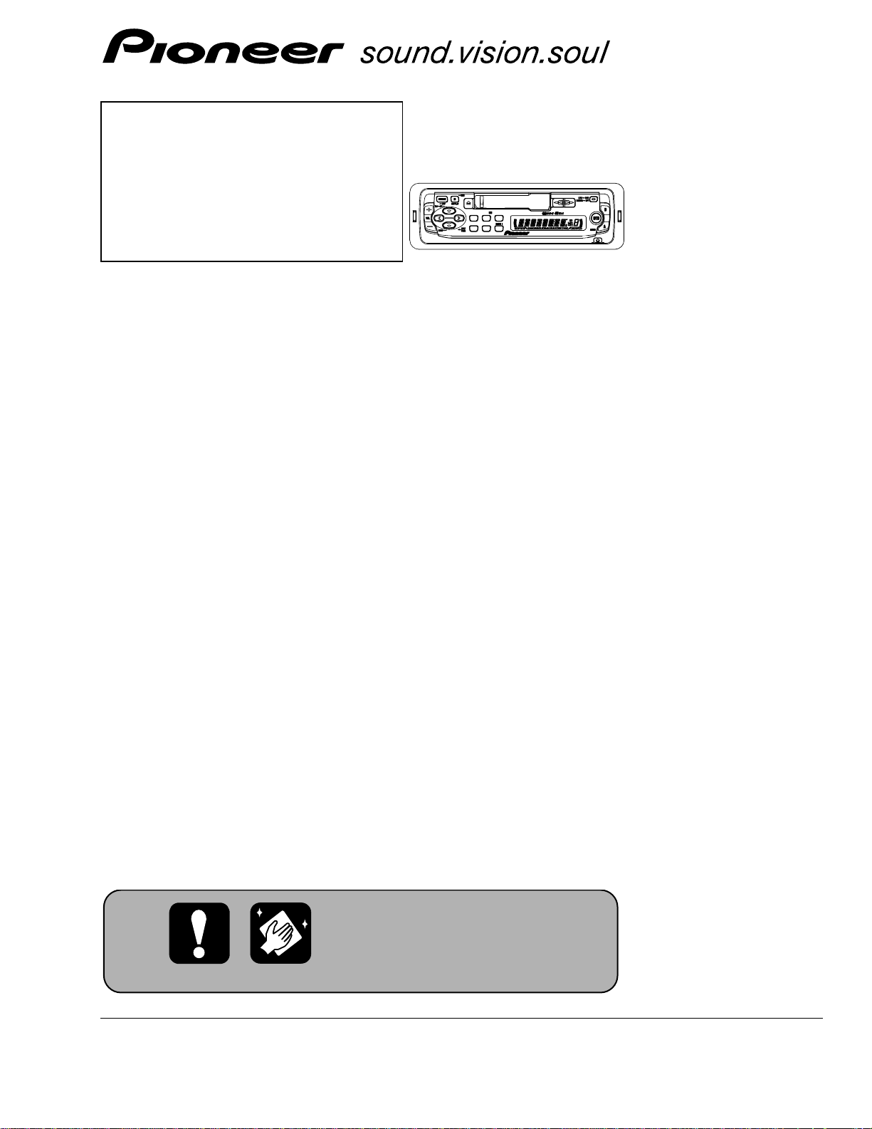
KEH-P2033RXM/EW
BANDBAND
BASS/TREBLE BOOSTERBASS/TREBLE BOOSTER
3
6
2
5
1
4
KEH-P2033R
KEH-P2033R/XM/EW
KEH-P2030R
XM/EW
For details, refer to "Important symbols for good services".
- This service manual does not describe the CD test mode.
For the operations in the CD test mode, refer to the CD player's Service manual.
CONTENTS
SAFETY INFORMATION ............................................2
1. SPECIFICATIONS........................................................3
2. EXPLODED VIEWS AND PARTS LIST.......................4
2.1 PACKING...............................................................4
2.2 EXTERIOR .............................................................6
2.3 CASSETTE MECHANISM ....................................8
3. BLOCK DIAGRAM AND SCHEMATIC DIAGRAM ...10
3.1 BLOCK DIAGRAM ..............................................10
3.2 OVERALL CONNECTION DIAGRAM.................12
3.3 KEYBOARD UNIT ...............................................14
3.4 CASSETTE MECHANISM ..................................16
4. PCB CONNECTION DIAGRAM ................................18
4.1 TUNER AMP UNIT .............................................18
4.2 KEYBOARD UNIT ..............................................22
4.3 CASSETTE MECHANISM ..................................24
5. ELECTRICAL PARTS LIST ........................................25
6. ADJUSTMENT..........................................................27
7. GENERAL INFORMATION .......................................28
7.1 DIAGNOSIS ........................................................28
7.1.1 DISASSEMBLY .........................................28
7.1.2 CONNECTOR FUNCTION DESCRIPTION ...29
7.2 PARTS .................................................................30
7.2.1 IC................................................................30
7.2.2 DISPLAY....................................................34
7.3 OPERATIONAL FLOW CHART ...........................35
7.4 CLEANING ..........................................................36
8. OPERATIONS ...........................................................37
2
1
234
12
34
F
E
D
C
B
A
KEH-P2033R/XM/EW
[ Important symbols for good services ]
In this manual, the symbols shown-below indicate that adjustments, settings or cleaning should be made securely.
When you find the procedures bearing any of the symbols, be sure to fulfill them:
2. Adjustments
To keep the original performances of the product, optimum adjustments or specification confirmation is indispensable.
In accordance with the procedures or instructions described in this manual, adjustments should be performed.
3. Cleaning
For optical pickups, tape-deck heads, lenses and mirrors used in projection monitors, and other parts requiring cleaning,
proper cleaning should be performed to restore their performances.
5. Lubricants, glues, and replacement parts
Appropriately applying grease or glue can maintain the product performances. But improper lubrication or applying
glue may lead to failures or troubles in the product. By following the instructions in this manual, be sure to apply the
prescribed grease or glue to proper portions by the appropriate amount.For replacement parts or tools, the prescribed
ones should be used.
4. Shipping mode and shipping screws
To protect the product from damages or failures that may be caused during transit, the shipping mode should be set or
the shipping screws should be installed before shipping out in accordance with this manual, if necessary.
1. Product safety
You should conform to the regulations governing the product (safety, radio and noise, and other regulations), and
should keep the safety during servicing by following the safety instructions described in this manual.
SAFETY INFORMATION
This service manual is intended for qualified service technicians; it is not meant for the casual do-it-yourselfer.
Qualified technicians have the necessary test equipment and tools, and have been trained to properly and safely repair
complex products such as those covered by this manual.
Improperly performed repairs can adversely affect the safety and reliability of the product and may void the warranty.
If you are not qualified to perform the repair of this product properly and safely, you should not risk trying to do so
and refer the repair to a qualified service technician.
3
5
6
7
8
F
E
D
C
B
A
5
6
7
8
KEH-P2033R/XM/EW
1. SPECIFICATIONS
Backup current....................Less than 3mA
4.76cm/sec. (+0.14cm/sec., -0.05cm/sec.)
4
1
234
12
34
F
E
D
C
B
A
KEH-P2033R/XM/EW
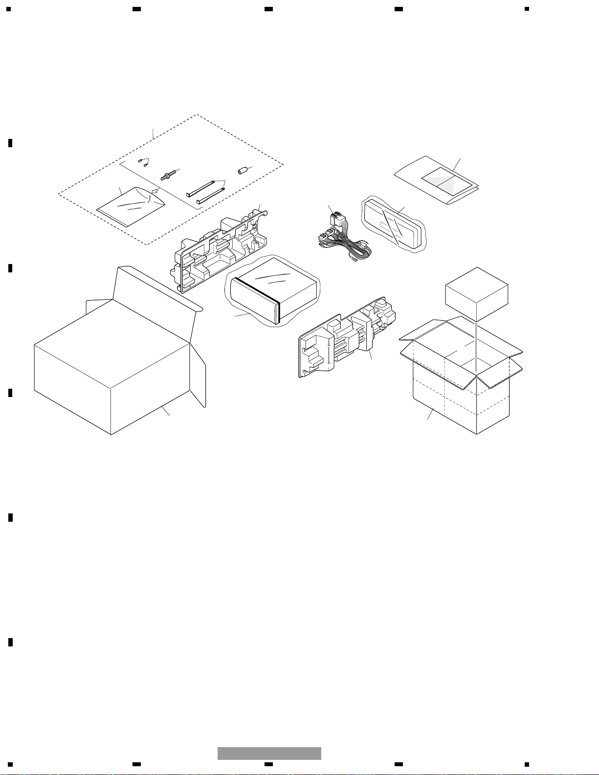
2. EXPLODED VIEWS AND PARTS LIST
2.1 PACKING
11
8
10
13
14
12
7
4
1
3
2
5
6
9
5
5
6
7
8
F
E
D
C
B
A
5
6
7
8
KEH-P2033R/XM/EW
1 Accessory Assy CEA3094
2 Screw CBA1002
3 Fixing Screw(M2x4) CBA1488
4 Handle CNC5395
5 Bush CNV3930
* 6 Polyethylene Bag E36-615
* 7-1 Passport CRY1013
* 7-2 Warranty Card CRY1157
7-3 Owner’s Manual CZR2959
7-4 Owner’s Manual CZR2960
7-5 Installation Manual CZR2961
8 Case Assy CXB3520
9 Cord Assy CZD2977
10 Polyethylene Bag CZE2903
11 Protector CZH5592
12 Protector CZH5591
13 Carton(KEH-P2033R) CZH6601
Carton(KEH-P2030R) CZH5599
14
Contain Box(KEH-P2033R) CZH6602
Contain Box(KEH-P2030R) CZH5600
Mark No. Description Part No. Mark No. Description Part No.
- PACKING SECTION PARTS LIST
NOTE:
- Parts marked by “*” are generally unavailable because they are not in our Master Spare Parts List.
- Screws adjacent to ∇ mark on the product are used for disassembly.
- For the applying amount of lubricants or glue, follow the instructions in this manual.
( In the case of no amount instructions, apply as you think it appropriate.)
- Owner's Manual, Installation Manual
Model Part No. Language
KEH-P2030R/XM/EW CZR2959 English, Spanish, German
KEH-P2033R/XM/EW CZR2960 French, Italian, Dutch
CZR2961 English, Spanish, German, French, Italian, Dutch
6
1
234
12
34
F
E
D
C
B
A
KEH-P2033R/XM/EW
2.2 EXTERIOR
7
5
6
7
8
F
E
D
C
B
A
5
6
7
8
KEH-P2033R/XM/EW
1 Screw BSZ26P060FMC
2 Button CAC4836
3 Door
See Contrast table(2)
4 Spring CBH1834
5 Spring CBH1835
6 Spring CBH1996
7 Bracket CNC6135
8 Bracket CNC6791
9 Arm CNV4692
10 Arm CNV4693
11 Arm CNV4728
12 Spring CZB2982
13 Cord Assy CZD2977
14 Plate CZN6730
15 Case CZN6739
16 Panel
See Contrast table(2)
17 Insulator CZN6836
18 Chassis
See Contrast table(2)
19 Tuner Amp Unit CZW5540
20 Screw BPZ26P100FZK
21 Screw BSZ26P100FMC
22 Fuse(10A) CEK1208
23 FM/AM Tuner Unit CWE1562
24 Holder CNC8815
25 Pin Jack(CN350) CKB1041
26 Connector(CN400) CKS3408
27 Connector(CN800) CKS3581
28 Antenna Jack(CN100) CKX1056
29 Connector(CN200) CZK2945
30 Connector(CN250) CZK2946
31 Connector(CN600) CZK2951
32 Connector(CN101) CZK2954
33 Rear Chassis CZN6834
34 Heat Sink CZN6835
35 Keyboard Unit
See Contrast table(2)
36 Connector(CN900) CKS3580
37 LCD(LCD900) CZA5579
38 Holder CZN6743
39 Connector CZN6745
40 Light Plate CZN6760
41 Lighting Conductor CZN6846
42 Rubber CZN6847
43 Sheet CZN6848
44 Screw BMZ26P040FMC
45 Bracket CZN6738
46 Mechanism CZX5514
47 Detach Grille Assy
See Contrast table(2)
48 Screw BPZ20P100FZK
49 Button(DETACH)
See Contrast table(2)
50 Button(FF) CZA5529
51 Button(REW) CZA5530
52 Button(EJECT) CZA5531
53 Button(SOURCE) CZA5566
54 Button(BTB) CZA5565
55 Button(1-6) CZA5564
56 Button(VOL) CZA5563
57 Spring CZB2976
58 Spring CZB2977
59 Cover
See Contrast table(2)
60 Screw IMS20P030FZK
61 Screw ISS26P055FUC
62 Transistor(Q604) 2SD2396
63 IC(IC500) TDA7384
Mark No. Description Part No. Mark No. Description Part No.
(1) EXTERIOR SECTION PARTS LIST
Part No.
Mark No. Symbol and Description KEH-P2033R/XM/EW KEH-P2030R/XM/EW
3 Door CAT2108 CAT2456
16 Panel CZN6757 CZN6867
18 Chassis CZN6856 CZN6855
35 Keyboard Unit CZW5544 CZW5543
47 Detach Grille Assy CZX5552 CZX5551
49 Button(DETACH) CAC5929 CAC7870
59 Cover CZN6754 CZN6753
(2) CONTRAST TABLE
KEH-P2033R/XM/EW and KEH-P2030R/XM/EW are constructed the same except for the following:
8
1
234
12
34
F
E
D
C
B
A
KEH-P2033R/XM/EW
2.3 CASSETTE MECHANISM

9
5
6
7
8
F
E
D
C
B
A
5
6
7
8
KEH-P2033R/XM/EW
Mark No. Description Part No. Mark No. Description Part No.
- CASSETTE MECHANISM SECTION PARTS LIST
1 Washer 1-0036-5024
2 Roller 1-0363-3018
3 Spring 1-0036-4011
4 Head(HD1) 1-0036-7123
5 Screw 1-0138-5002
6 Screw 2-1012-0040-C2
7 Plate 1-0036-1015
8 Spring 1-0036-4010
9 Arm 10138-2005-3
10 Shim 1-0138-1006
11 Pinch Arm (F) Assy 1-0036-6014
12 Spring 1-0363-4003
13 Screw 2-1032-0070-C2
14 Tape Guide 1-0038-2018
15 Link 1-0363-2006
16 Pinch Arm (R) Assy 1-0036-6013
17 Spring 1-0363-4004
18 Motor Assy (M1) X-0363-7006
19 Power Switch (S1) 1-0363-7005
20 Mute Switch (S2) 1-0363-7001
21 Screw 213317040-C2
22 Screw 2-1032-0025-C2
23 Arm Assy X-0363-6003
24 Slide Switch (S3) 1-0363-7002
25 SW PWB 1-0363-7008
26 Belt 1-0036-5018
27 Screw 213820030-C2
28 Belt 1-0036-5004
10
1
234
12
34
F
E
D
C
B
A
KEH-P2033R/XM/EW
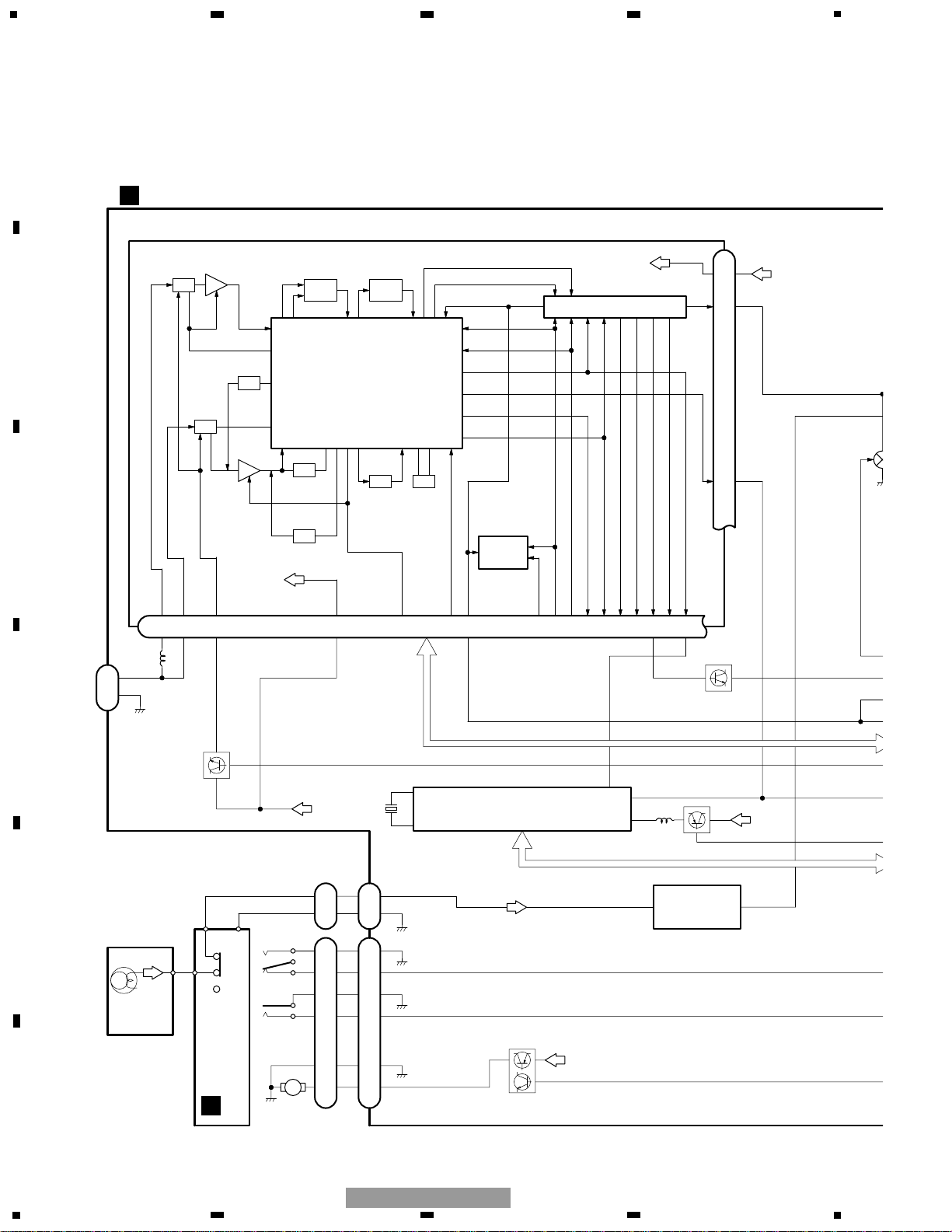
3. BLOCK DIAGRAM AND SCHEMATIC DIAGRAM
3.1 BLOCK DIAGRAM
CASSETTE MECHANISM
IC 3
VCC
VCC
IC 2 FM MPX
IC 1
MIXER,IF,AMP,DET.
LDET
Lch
22
AM ANT
FM ANT
LOCL
LOCH
CK
ATT
10
6
18
28 27 25 23
CREQ
DI/DO
CE2
19 14 12
CE1
SDBWSLFMSD
NL1
NL2
STIND
COMP
15 16 218234113
AM RF
ATT
ANT ADJ
FM RF
T51,Q51
CF51,CF52,CF53
FM/AM 1ST IF 10.7MHz
MPXREF 41kHz
AMDET
IMG ADJ
RF ADJ
AM 2ND IF
450kHz
CF202
EEPROM
X901
10.25MHz
B.U5V
Q150
12
Q101
COM9V
8
20
61
23
15
11
12
1
2
RDS DECODER
Q100
B.U5V
IC150
PM4009A
IC200
BA4560F
EQ-AMP
5
11
24
CN100
ANT.
37
TUNER AMP UNIT
FM/AM TUNER UNIT
A
8
7
6
5
2
1
1
3
8
7
6
2
1
5
SWITCH PCB
M1
MOTOR ASSY
M
S1
TAPE/TUN
S2
MUTE
HD1
HEAD
1
3
Q250
Q251
LCH
MOTOR+
CN250
CN200
B.U14V
28
C
7
11
5
6
7
8
F
E
D
C
B
A
5
6
7
8
KEH-P2033R/XM/EW
CN400
BU
1
3
CN350
GND
LCH
Q351
Q350
Q500
45
TAPE IN
LDET
61
LOCL
23
NL2
Q130
22
MUTE
VCC1
VCC2
4
15
FL-
ACC
CN600
5
6
7
1
FL+
RL+
RL-
GND
16
ILL14V
89
11
TUNPDI
12
TUNPDO
45
PEE
Q603
Q602
B.U5V
Q501
B.U5V
Q606
Q607
Q604
COM9V
IC2
PST3434UL
RESET
B.U5V
1
2
IC600
TPD1018F
1
11
5
B.REM
Q600
Q601
10
6
56 57 58 60
5
54
69
70
66
55
65
Q800
B.U5V
2
8
CN800
DGND
ILLGND
MUTE
SYSPW
X2
X1
BSENS
B.REM
ASENS
TX
RX
ASENB0
RESET
3
SW5V
7
1
6
39
SWVDD
KEYBOARD UNIT
Q605
IC1
000974500
SYSTEM CONTROLLER
Q400
Q401
B.U14V
IC300
PML010A
ELECTRONIC VOLUME
18711
BUS +
BUS -
SWDB
BUSL +
IC400
HA12187FP
65
5
12
6
5
2
4
37
IN4-L
IN4+L
IN1L
IN3L
FM/AM
11
10
OUT_RL
OUT_FL
BUSL -
IC500
TDA7384
POWER AMP
15
IN3 RL
11
IN1 FL
4
STB
IP-BUS
DRIVER
7
9
17
19
IC900
PD6340A
CN900
8
56
VDD
22
23
XO
XI
LCD
KEY MATRIX
B
MOTOR
53
FFREW
48
28
TMUTE
IP BUS
REAR OUT
12
1R8KR253
33
R204
2PB709A
Q400
100/10
C207
1SS133
D802
470P
C210
C200
15K
R209
11ES2
D250
1/4W
3R3
R250
R1
C400
47K
R200
GND3
22K
R403
820
R401
62
R407
1SS133
D804
47K
R416
47K
R201
1K
R414
R001
C401
1SS133
D200
1K
R413
GND1
10
R212
2R2KR800
1SS133
D800
1SS133
D801
560K
R207
R01
C209
GND1
47K
R803
1R8KR252
10K
R251
2R2KR409
22P
C201
100P
C205
GND1
2R2K
R802
R001
C202
4R7K
1SS133
D805
2R2uH
L400
R001
C203
1SS133
D803
47K
R415
1K
R412
33
R205
2R2K
R801
22P
100
R408
100
R406
1KR404
22K
R402
1K
R211
1K
R210
2SA1706Q250
5
6
8
7
DTC114EK
Q401
DTC114EK
Q251
100
R202
100
R203
1KR405
820
R400
1
OUT1
2
IN-1
3
IN+1
4
GND
IN+2
IN-2
VCC
OUT2
20
+
9
321
456
1
2
3
456
2R7K
R132
47KR106
22K
R134
47KR113
4R7uH
L100
22K
R135
1uHL102
680R107
680R103
1R6K
R130
47KR121
470KR115
R0022
C131
47KR102
330PC110
1R6K
R131
2R2KR101
680R118
R022
C102
2R7K
R133
R01
C133
680R109
2R2K
R100
1uHL101
R001
C101
2R2/50
C135
R047C106
GND4
4R7KR108
10K
R111
47KR119
680R105
R01
C132
R0022
C130
680R112
Q150
R0047C105
2R2/50
C134
R022
C100
R0015C109
47KR104
R0047C108
47KR120
15K
R117
R01C103
2PD601A
Q101
39KR110
1KR114
1
STIND2FMSD3NL14NL25R6L7WC8SDBW
10
VDD11DGND
12
CE213SL14DI/DO15CK16CE117NC1718LDET19CREQ
21
COMP22VCC23LOCH24FMLOCL
25
LOCL26RFGND
27
FMANT
28
AMANT
680R116
100/10C107
100/10
C104
47KR157
ET100
IMH3A
Q130
R01C112
DSP-201M-A11F
DSP100
LOCL
LOCH
CREQ
TUCE1
TUDT
SL
NL1
TUCK
DRST
TMUTE
STIND
FMSD
TU-RCH
TUCE2
TU-LCH
"CN101"
1
VDD-D2TRESET3HSRDS4CLOCK5DATA6RDS7HSRDS28HSRESET9D-SUB10D-GND11XI12XO
13
TPIN314TPIN2
15
RESET
16
A-GND
17
A-SUB
18
VREF
19
REF
20
MPX_IN
21
TESTMODE
22
MODECK
23
TPIN1
24
VDD-A
27PC154
GND6
R1
C153
R1
C151
1KR150
1KR155
10uHL150
470PC158
680R154
27P
C155
1KR152
2R2MR156
22/16
C152
470PC157
22/16
C150
DTA124EK
100uH
L151
680R153
1KR151
R1C156
3.648MHz
X150
RDS57K
RDSLK
RDT
RCK
FM/AM
LDET
GND4
C-LCH
B-RCH+
B-LCH+
ASENBO
B-RCH-
B-LCH-
C-RCH
IPPW
TX
RX
GND3
GND2
GND1
MOTOR+
MOTOR-
N/R
FFREW
TAPE_IN
AGND
RCH
LCH
GND
S2
ROUT
S1
BUS-
BUS+
VCC
STB
BUSL-
BUSR-
BUSR+
BUSL+
SWDB
BUS-
BUS+
DSENS
DGND
SW5V
NC
KYDT
DPDT
ILL+B
ILLGND
2
3
4
5
8
6
7
1
9
11
10
+
+
+
15K
R208
R01
C212
10KR213
100/6R3
C206
22K
R410
100K
R254
10/16
C211
100P
C204
R01
C208
10K
R214
33/10
C213
100K
R255
R411
560K
R206
100K
R256
1
2
3
4
56 87
1
1C309
R22C306
10P
C313
C307
R1C301
R22C305
10P
C315
R22C303
R22C304
10PC316+10PC314
4R7uH
L300
1C308
1C310
1K
R2
1KR16
1K
R1
4R7
C311
4R7C312
1234567891011121314
1516171819202122232425262728
10/16
C302
47/16
C300
12345678910111213141516171819
20
TMUTE
B-RCH-
B-RCH+
C-RCH
TU-RCH
TU-LCH
C-LCH
B-LCH+
B-LCH-
VCK
MUTE
KYDT
DPDT
TUDT
TUCK
TUCE1
VST
VDT
VCK
VREF
IN1L
AGND
IN2L
IN3L
IN4+L
IN4-L
LOUDOUT_L
SVIN_L
OUT_FL
OUT_RLNCDGND
CLK
LOUDOUT_R
SVIN_R
OUT_FR
AGND
VCC
IN2R
IN4+R
IN4-R
IN3R
IN1R
NC
STB
DATA
OUT_RR
61
R1
C801
2R2K
R805
GND2
10uHL800
22K
R806
1/4W
4R7
R804
2PB709A
Q800
R1
C800
2R2K
R807
21
22
23
24
25
26
27
28
29
30
31
32
33
34
35
36
37
38
39
40
41424344454647484950525354555657585960
62
63
64
65
66
67
68
69
70
71
72
73
74
75
76
77
78
79
80
LOCL
LOCL
LOCH
LOCH
CREQ
CREQ
TUCE2
TUCE2
SDBW
SDBW
NL2
NL2
STIND
680
R3
680
R4
DRST
DRST
RDSLK
RDSLK
PEE
PEE
RDS57K
RDS57K
TX
RX
FFREW
FFREW
NC(RECEIVE)
TX
RX
RCK
RDT
NL1
NC
XT2
TMUTE
TAPE
FFREW
F/R
MOTOR
FMSD
FM/AM
SWVDD
F/R
MOTOR
SYSPW
B.REM
ASENBO
IPPW
SWVDD
ILL+B
DSENS
KYDT
DPDT
TAPE
NC(ADPW)
AVSS
MUTE
AVREF1
KYDT
DPDT
TUNPDI
TUNPDO
TUNPCK
TUNPCE
VST
VDT
VCK
SD
ST
VSS1
FM/AM
SWVDD
TAPE_IN
NC(PCL)
F/R
MOTOR
SYSPW
B.REM
ASENBO
IPPW
RESET
LDET
DSENS
ASENS
BSENS
VDD1
X2
X1
IC
XT1(TEST)
VDDO
AVREFO
SL
51
+
GND5
2PD601A
Q100
GND1
SDBW
NL2
R01C5
+
GND2
"AR100"
+
+
+
+
GND1
+
FM -27.5dBs
AM -27.5dBs
TAPE-7dBs
PML010AIC300
FM -23dBs
AM -23dBs
TU100
TUNER AMP UNIT
FM/AM TUNER UNIT
ANT
CN100
RDS
PM4009A
IC150
BA4560F
IC200
EQ-AMP
CN200
CASSETTE MECHANISM
CN250
CN400
IP BUS
CN900
CN800
KEYBOARD UNIT
ASENBO
SYSTEM CONTROLLER
000974500IC1
HA12187FP
IC400
BUS
231
8
7
6
5
4
3
2
1
1
2
3
4
5
6
7
8
1
2
3
1
2
3
4
5
6
7
8
1
2
3
5
6
7
8
9
10
11
4
7
6
5
4
1
3
2
8
2
1
3
B
C
A
1
234
12
34
F
E
D
C
B
A
KEH-P2033R/XM/EW
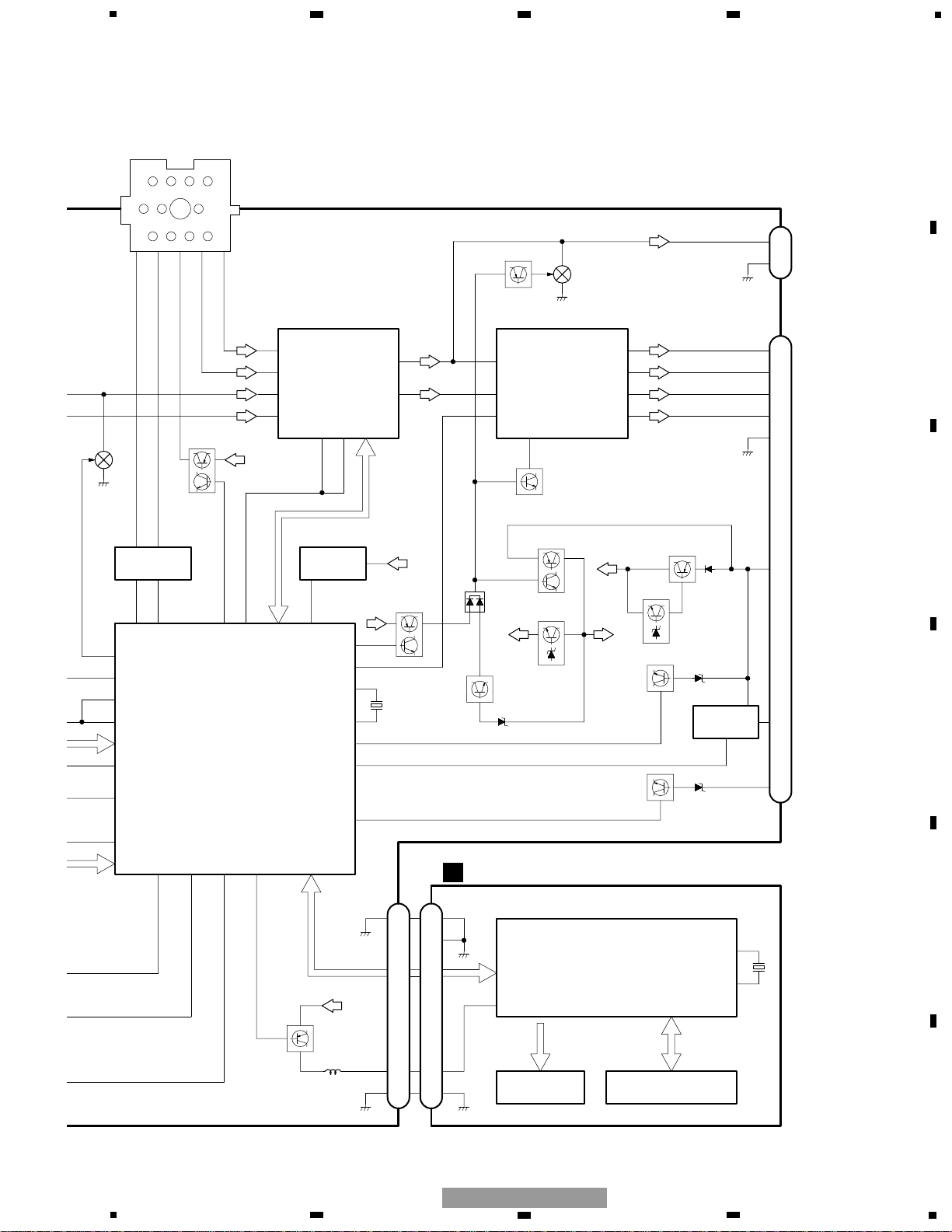
3.2 OVERALL CONNECTION DIAGRAM
Note: When ordering service parts, be sure to refer to “EXPLODED VIEWS AND PARTS LIST” or “ELECTRICAL PARTS
LIST”.
A

13
5
6
7
8
F
E
D
C
B
A
5
6
7
8
KEH-P2033R/XM/EW
A
+
VDT
VST
10P
C313
10P
C315
10PC316
100R305
100R302
100R303
10PC314
100R304
10/16
C3
R1
C2
91011121314
151617181920
1
2
4R7K
R300
R01
C318
4R7K
R301
R01
C317
PEE
VCK
SVIN_L
OUT_FL
OUT_RLNCDGND
CLK
SVIN_R
OUT_FR
NC
STB
DATA
OUT_RR
61
+
47K
R8
1K
R6
GND3
47K
R5
D2
R9 100K
2R2/50
C4
6.29MHz
X1
1SS355
D1
1
VOUT
2
VDD
3
NC
4
VSS
59
60
62
63
64
65
66
67
68
69
70
71
72
73
74
75
76
77
78
79
80
2R2KR7
TX
RX
RCK
RDT
NL1
NC
XT2
MUTE
IPPW
IPPW
RESET
LDET
DSENS
ASENS
BSENS
VDD1
X2
X1
IC
XT1(TEST)
VDDO
AVREFO
SL
HZS7L(A1)
D603
R604
R001
C602
100KR603
47K
R606
11ES2
D605
22K
R605
11ES2D604
R047
C604
12345
GND
GND
GND
OUT
VCC
GND
56113
1
87104
9
16
15
14 13
12
2
+
R47
C502
R47
C500
1R5K
R611
1K
R1
C603
2SD2396
Q604
10K
R607
2PD601A
Q601
2R2uH
L1
10K
R614
R01
C611
22K
R613
1R2K
R609
47K
R602
HZS9L(A2)
D609
R610
2PD601A
Q605
D608
1R8K
R616
1R8K
R615
100/10
C612
10K
R612
100P
C1
689107
2SA2112
Q606
DTC114EK
Q607
GND1
FL
B.REM
FR
RR
FL
RL
ASENS
ILL+B
IN
GND
GND
GND
DIAG
+
+
+
220
R503
R47
C501
10K
R501
R1
C512
GND2
2R2/50C351
2R2
C510
R47
C503
15K
R502
IMD2AQ501
1
2
3
4
5
6
2R2
C509
R47
C505
DTC124EK
Q500
33/10
C511
820
R351
R47
C507
DAN202U
D500
10/16
C508
2R2/50C350
R47
C506
100
R504
DTA124EK
Q351
R47
C504
R1
C513
10K
R500
3
2
16
5
4
1
2
3
4
5
6
7
8
9
10
11
12
13
14
15
16
17
18
19
20
21
22
23
24
25
820R350
1R5K
R505
RCK
RDT
NL1
GND1
RL
RR
FR
SYSPW
ASENS
BSENS
SL
LDET
+
R0022
C352
R0022
C353
47K
R353
47K
R352
321
456
GND1
IMH3A
Q350
1
2
3
456
RCH
GND
LCH
+
+
+
22K
R608
R01
C607
R01
C606
11ES2
D606
47/16
C605
470/16C608
GND1
2PD601A
Q603
HZS6L(B2)
D607
R01C610
270
HZS9L(B3)
100/10C609
R001
C516
R001
C517
R001
C518
R001
C519
R001
C520
R001
C521
R001
C522
R001
C523
2SB1181F5
Q602
RL+
FL+
FL-
RL-
FR+
FR-
RR-
RR+
+
11ES2
D600
100KR600
3300/16
C600
11ES2
D601
HZS7L(C2)
D602
2PD601A
Q600
47K
R601
GND1
R1
C601
BSENS
CEK1208
10A
L600
FR-
FR+
FL-
FL+
RL+
RL-
RR+
RR-
FR-
FR+
FL-
FL+
RL+
RL-
RR+
RR-
ACC
B_REM
BU
600uH
DSENS
!
NOTE :
Decimal points for resistor
and capacitor fixed values
are expressed as :
2.2 2R2
0.022 R022
←
←
The > mark found on some component parts indicates
the importance of the safety factor of the part.
Therefore, when replacing, be sure to use parts of
identical designation.
FM -2.5dBs
AM -2.5dBs
TAPE 0dBs
RESET
PST3434ULIC2
ELECTRONIC
VOLUME
B.REM
CN600
DC_CONNECTOR
ASENSE
BSENSE
TPD1018F
IC600
SW14V
COM9V
BU5V
POWER AMP
CN350
REAR OUT
FM -3dBs
AM -3dBs
TAPE-0.5dBs
TDA7384IC500
123456789
10 11 12 13 14 15 16 17 18
1
2
3
MUTE

14
1
234
12
34
F
E
D
C
B
A
KEH-P2033R/XM/EW
GND9
KEYBOARD UNIT
PD6340A
IC900
123456789
10111213141516
17
18
19
20
21
22
23
24
25
26
27
28
29
30
31
32
33
34
35
36
37
38
39
40
41
42
43
44
45
46
47
48
49
50
51
52
53
54
55
56
57
58
59
60
61
62
63
64
2R2
C901R1C900
47K
R903
470
RN901
470
RN900
4.97MHz
X900
LCD900 CZA5579
151015202530354042
SEG38
SEG37
SEG36
SEG35
SEG34
SEG33
SEG32
SEG31
SEG29
SEG28
SEG30
SEG22
SEG27
SEG25
SEG24
SEG23
SEG21
SEG26
SEG20
SEG19
SEG18
SEG17
SEG16
SEG14
SEG15
SEG13
SEG7
SEG9
SEG12
SEG8
SEG10
SEG11
SEG6
SEG5
SEG4
SEG3
SEG1
SEG2
COM3
COM0
COM2
COM1
KDT1
KDT0
KST0
KST1
KST2
KST3
COM0
COM1
COM3
SEG2
SEG1
SEG4
SEG3
SEG12
SEG6
SEG11
SEG5
SEG9
SEG10
SEG8
SEG7
SEG28
SEG20
SEG14
SEG27
SEG21
SEG25
SEG26
SEG24
SEG23
SEG13
SEG22
SEG17
SEG18
SEG16
SEG15
SEG34
SEG30
SEG31
SEG32
SEG33
SEG35
SEG37
SEG29
SEG36
SEG38
COM2
SEG19
SEG4
SEG3
SEG2
SEG1
SEG0
COM3
COM2
COM1
COM0
LCDB
KST3
KST2
KST1
KST0
KDT0
KDT1
REM
DPDT
RST
KYDT
MODA
XO
XI
VSS
KDT2
KDT3
NC
SEG37
SEG39
SEG38
SEG36
KST4
SEG35
SEG34
SEG33
SEG32
SEG31
SEG30
SEG29
SEG28
SEG27
SEG26
SEG25
SEG24
SEG23
SEG22
SEG21
SEG20
SEG19
SEG18
SEG17
SEG16
SEG15
SEG14
SEG13
VDD
SEG12
SEG11
SEG10
SEG9
SEG8
SEG7
SEG6
SEG5
B
3.3 KEYBOARD UNIT
B

15
5
6
7
8
F
E
D
C
B
A
5
6
7
8
KEH-P2033R/XM/EW
B
GND8
CN800
A
14V 65mA
10R900
2R2KR902
2R2KR901
HZM6R2ZWA
D900
SW927
SW903
SW919
SW923
SW914
SW902
SW921
SW910
SW912
SW901
SW918
SW900
SW926
SW928
SW929
SW920SW907
SW916
SW905
SW924
SW931
SW922
SW917
SW909
SW904
SW915
SW925
SW911
SW906 SW913
SW908
SW930
CN900
1
2
3
4
5
6
7
8
PL902
PL901
PL900
KDT3
KDT2
KST4
KDT0
KDT1
KDT2
KST4
KDT3
KST0
KST1
KST2
KST3
DESNS
DGND
SW5V
NC
KYDT
DPDT
ILL+B
ILLGND
LOCAL
BTB
4
1
VOL
-
AUDIO
BAND
6
2
SOURCE
LOUD
3
DISP
CLOCK
5
VOL
+
KEH-P2030R
KEH-P2033R
CZE2950
CZE2958
IVORY
VW_RED

16
1
234
12
34
F
E
D
C
B
A
KEH-P2033R/XM/EW
3.4 CASSETTE MECHANISM
C
TUNER AMP UNIT
A
A
CN200
C
SWITCH PCB
C
GND
Rch
Lch
3
3
2
2
1
1
Rch
Lch
HD1
HEAD
1-0036-7123
Rch
Lch
S3
FWD/REV
1-0363-7002
CN250
GND3
8
S1
TAPE/TUN
1-0363-7005
MUTE
1-0363-7001
S2
M
M1
MOTOR ASSY
X-0363-7006
TAPE-IN
GND2
FF/REW
GND1
N/R
MOTOR-
MOTOR+
8
7
7
6
6
5
5
4
4
3
3
2
2
1
1

17
5
6
7
8
F
E
D
C
B
A
5
6
7
8
KEH-P2033R/XM/EW

18
1
234
12
34
F
E
D
C
B
A
KEH-P2033R/XM/EW
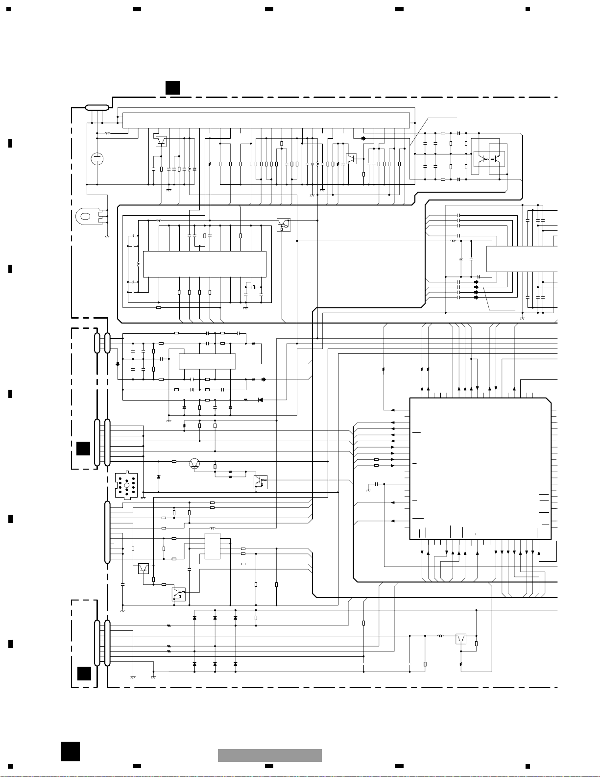
4. PCB CONNECTION DIAGRAM
4.1 TUNER AMP UNIT
NOTE FOR PCB DIAGRAMS
1. The parts mounted on this PCB
include all necessary parts for
several destination.
For further information for
respective destinations, be sure
to check with the schematic dia-
gram.
2. Viewpoint of PCB diagrams
Capacitor
Connector
P.C.Board
Chip Part
SIDE A
SIDE B
A
1357
4268
B
C
BUS CONNECTOR
CORD ASSY
123
4
567
89
10
11
CN400
17
CN600
18
1
2
3
4
5
6
7
8
R600R603
R604
R800
R801
R802
R610
R615
R616
CN800
R254
C605
C608
C609
C612
CN250
C3
C4
D600
D601
D602D603
D604
D605
D606
D607
D608
D609
D800
D801
D802
D803
D805
D250
L1
R6
R7
L400
L600
L800
X1
+
+
+
+
+
+
Q606
Q604
E
E
123456712345678
910
111213
14
15
8
16
D804
CN900
TUNER AMP UNIT
A

19
5
6
7
8
F
E
D
C
B
A
5
6
7
8
KEH-P2033R/XM/EW
A
FRONT
Q604
Q606
Q250
IC500
IC,Q
C
PRE OUT
ANTENNA
1
2
345
678
910111213
14 161820 22 24
151719 21 23 25
1
2
CN100
3
CN350
2
3
1
1
2
3
4
5
6
7
8
10
11
12
13
14
15
16
17
18
19
21
22
23
24
25
26
27
28
R210
R211
R212
CN200
R807
TU100
C206
C207
C211
C213
R252
R253
C600
D200
L100
L101
L102
D600
L300
D601
D606
DSP100
L150
L151
R116
C104
C107
C300
C302
R157
C508
R16
C511
C134
C135
R1
R2
C150
C152
C350
C351
X150
IC500
ET100
+
+
+
+
+
+
+
+
+
+
+
+
+
+
+
+
Q250
E
+
SIDE A

20
1
234
12
34
F
E
D
C
B
A
KEH-P2033R/XM/EW
C108
C352
8
1
C200
C201
C202
C203
C204
C205
C208
C209
C210
C212
Q100
Q101
Q130
Q351
C100
C101
C102
C103
C105
C106
C109
C303
C110
C304
C305
C112
C306
C307
C308
C309
C500
C501
C502
C503
C310
C504
C311
C505
C312
C506
C313
C507
C314
C315
C509
C316
C317
C318
C510
C513
C130
C131
C132
C133
C154
C155
C156
C157
C158
C353
D500
R213
R214
JC1
JC2
JC3
JC5
JC6
JC8
R100
R101
R102
R103
R104
R105
R106
R107
R108
R109
R300
R301
R302
R303
R110
R304
R111
R305
R112
R113
R114
R115
R117
R118
R119
R
R502
R503
R504
R120
R121
R130
R131
R132
R133
R134
R135
R154
R155
R156
R350
R351
R352
R353
R3
R4
R200
R201
R202
R203
R204
R205
R206
R207
R208
R209
IC,Q
Q350
Q351,Q251
IC600
Q400
IC300
Q100
IC150
Q605
IC400
Q600
Q603,Q602
IC200
Q150,Q800
Q500
Q401
Q607,Q601
Q501
IC1
IC2
Q130
Q101
E
E
E
E
1
3
4
6
1
3
4
6
5
4
5
15
1
20
10
13
12
24
C153
C151
5
10
20
25
1
14
15
28
C301
JC4
IC150
Q500
IC200
Q350
IC300
1
1
A
TUNER AMP UNIT
A

21
5
6
7
8
F
E
D
C
B
A
5
6
7
8
KEH-P2033R/XM/EW
C5
C318
C512
D500
Q251
R400
R401
R402
R403
R404
R405
R611
R250
R251
R500
R501
R502
R503
R150
R151
R152
R153
R154
E
35
30
25
15
10
5
75
70
65
55
50
45
C400
C401
C601
C602
C603
C604
C606
C607
C800
C801
C610
C611
C1
C2
D1
Q501
IC600
Q150
IC2
C516
C517
C518
C519
C520
C521
C522
C523
Q400
Q401
Q600
Q601
Q602
Q605
Q607
Q800
R406
R407
R408
R409
R601
R602
R410
R411
R605
R412
R606
R413
R607
R414
R608
R415
R609
R416
R417
R803
R804
R805
R612
R613
R614
R255
R256
R505
R5
R8
R9
E
E
E
E
E
E
E
E
E
1
3
4
6
R806
10
5
20
21
40
41
60
61
801
1
5
6
1
4
8
1
23
4
E
IC400
Q603
IC1
1
1
1
1
A
SIDE B

22
1
234
12
34
F
E
D
C
B
A
KEH-P2033R/XM/EW
4.2 KEYBOARD UNIT
B
IC,Q
IC900
KEYBOARD UNIT
PL900
1
2
7
8
CN900
3
5
4
6
CN800
PL902
R900
R901
R902
C900
C901
D900
B
A
B
KEYBOARD UNIT
CLOCK
LOUD
SW908
VOL-
VOL+
SW931
SOURCE
DISP
1
2
3
4
5
6
42
40
35
SW915
SW916
SW921
SW922
SW927
SW928
SW925
SW926
SW917
SW918
SW923
SW924
SW906
SW907
SW913
SW914
SW919
SW920
SW904
SW905
SW929
SW930
SW911
SW912

23
5
6
7
8
F
E
D
C
B
A
5
6
7
8
KEH-P2033R/XM/EW
B
SIDE A
SIDE B
LOCAL
SW909
SW910
BAND
SW900
35
30 25
LCD900
20
15
10
5
1
SW901
SW903
BTB
SW902
AUDIO
RN901
X900
R903
32
16
17
IC900
33
49
48
RN900
1
64
PL901

24
1
234
12
34
F
E
D
C
B
A
KEH-P2033R/XM/EW
4.3 CASSETTE MECHANISM
C
CN250
A
8 543216
7
S1
TAPE/TUN
M1
M
MOTOR ASSY
S2
MUTE
S3
FWD/REV
S3
A
CN200
123
C
SWITCH PCB
C
1
2
3
1
2
Rch Lch
3
HD1
HEAD

25
5
6
7
8
F
E
D
C
B
A
5
6
7
8
KEH-P2033R/XM/EW
5. ELECTRICAL PARTS LIST
NOTE:
- Parts whose parts numbers are omitted are subject to being not supplied.
- The part numbers shown below indicate chip components.
Chip Resistor
RS1/_S___J,RS1/__S___J
Chip Capacitor (except for CQS.....)
CKS....., CCS....., CSZS.....
Unit Number : CZW5540
Unit Name : Tuner Amp Unit
MISCELLANEOUS
IC 1 IC 000974500
IC 2 IC PST3434UL
IC 150 IC PM4009A
IC 200 IC BA4560F
IC 300 IC PML010A
IC 400 IC HA12187FP
IC 500 IC TDA7384
IC 600 IC TPD1018F
Q 100 Transistor 2PD601A
Q 101 Transistor 2PD601A
Q 130 Transistor IMH3A
Q 150 Transistor DTA124EK
Q 250 Transistor 2SA1706
Q 251 Transistor DTC114EK
Q 350 Transistor IMH3A
Q 351 Transistor DTA124EK
Q 400 Transistor 2PB709A
Q 401 Transistor DTC114EK
Q 500 Transistor DTC124EK
Q 501 Transistor IMD2A
Q 600 Transistor 2PD601A
Q 601 Transistor 2PD601A
Q 602 Transistor 2SB1181F5
Q 603 Transistor 2PD601A
Q 604 Transistor 2SD2396
Q 605 Transistor 2PD601A
Q 606 Transistor 2SA2112
Q 607 Transistor DTC114EK
Q 800 Transistor 2PB709A
D 1 Diode 1SS355
D 200 Diode 1SS133
D 250 Diode 11ES2
D 500 Diode DAN202U
D 600 Diode 11ES2
D 601 Diode 11ES2
D 602 Diode HZS7L(C2)
D 603 Diode HZS7L(A1)
D 604 Diode 11ES2
D 605 Diode 11ES2
D 606 Diode 11ES2
D 607 Diode HZS6L(B2)
D 608 Diode HZS9L(B3)
D 609 Diode HZS9L(A2)
D 800 Diode 1SS133
D 801 Diode 1SS133
D 802 Diode 1SS133
D 803 Diode 1SS133
D 804 Diode 1SS133
D 805 Diode 1SS133
L 1 Inductor LAU2R2J
L 100 Ferri-Inductor LAU4R7J
L 101 Ferri-Inductor LAU1R0J
L 102 Ferri-Inductor LAU1R0J
L 150 Ferri-Inductor LAU100J
L 151 Ferri-Inductor LAU101J
L 300 Ferri-Inductor LAU4R7J
L 400 Inductor LAU2R2J
L 600 Choke Coil 600µH CTH1221
L 800 Ferri-Inductor LAU100J
X 1 Ceramic Resonator 6.29MHz CSS1310
X 150 Crystal Resonator 3.648MHz CSS1447
DSP 100 Surge Protector DSP-201M-A11F
TU 100 FM/AM Tuner Unit CWE1562
RESISTORS
R 1 RD1/4PU102J
R 2 RD1/4PU102J
R 3 RS1/16S681J
R 4 RS1/16S681J
R 5 RS1/16S473J
R 6 RD1/4PU102J
R 7 RD1/4PU222J
R 8 RS1/16S473J
R 9 RS1/16S104J
R 16 RD1/4PU102J
R 100 RS1/16S222J
R 101 RS1/16S222J
R 102 RS1/16S473J
R 103 RS1/16S681J
R 104 RS1/16S473J
R 105 RS1/16S681J
R 106 RS1/16S473J
R 107 RS1/16S681J
R 108 RS1/16S472J
R 109 RS1/16S681J
R 110 RS1/16S393J
R 111 RS1/16S103J
R 112 RS1/16S681J
R 113 RS1/16S473J
R 114 RS1/16S102J
R 115 RS1/16S474J
R 116 RD1/4PU681J
R 117 RS1/16S153J
R 118 RS1/16S681J
R 119 RS1/16S473J
R 120 RS1/16S473J
R 121 RS1/16S473J
R 130 RS1/16S162J
R 131 RS1/16S162J
R 132 RS1/16S272J
R 133 RS1/16S272J
R 134 RS1/16S223J
R 135 RS1/16S223J
R 150 RS1/16S102J
R 151 RS1/16S102J
=====Circuit Symbol and No.===Part Name Part No.
--- ------ ------------------------------------------ -------------------------
=====Circuit Symbol and No.===Part Name Part No.
--- ------ ------------------------------------------ -------------------------
A

26
1
234
12
34
F
E
D
C
B
A
KEH-P2033R/XM/EW
R 152 RS1/16S102J
R 153 RS1/16S681J
R 154 RS1/16S681J
R 155 RS1/16S102J
R 156 RS1/16S225J
R 157 RD1/4PU473J
R 200 RS1/16S473J
R 201 RS1/16S473J
R 202 RS1/16S101J
R 203 RS1/16S101J
R 204 RS1/16S330J
R 205 RS1/16S330J
R 206 RS1/16S564J
R 207 RS1/16S564J
R 208 RS1/16S153J
R 209 RS1/16S153J
R 210 RD1/4PU102J
R 211 RD1/4PU102J
R 212 RD1/4PU100J
R 213 RS1/16S103J
R 214 RS1/16S103J
R 250 RS1/8S3R3J
R 251 RS1/16S103J
R 252 RD1/4PU182J
R 253 RD1/4PU182J
R 254 RD1/4PU104J
R 255 RS1/16S104J
R 256 RS1/16S104J
R 300 RS1/16S472J
R 301 RS1/16S472J
R 302 RS1/16S101J
R 303 RS1/16S101J
R 304 RS1/16S101J
R 305 RS1/16S101J
R 350 RS1/16S821J
R 351 RS1/16S821J
R 352 RS1/16S473J
R 353 RS1/16S473J
R 400 RS1/16S821J
R 401 RS1/16S821J
R 402 RS1/16S223J
R 403 RS1/16S223J
R 404 RS1/16S102J
R 405 RS1/16S102J
R 406 RS1/16S101J
R 407 RS1/16S620J
R 408 RS1/16S101J
R 409 RS1/16S222J
R 410 RS1/16S223J
R 411 RS1/16S472J
R 412 RS1/16S102J
R 413 RS1/16S102J
R 414 RS1/16S102J
R 415 RS1/16S473J
R 416 RS1/16S473J
R 500 RS1/16S103J
R 501 RS1/16S103J
R 502 RS1/16S153J
R 503 RS1/16S221J
R 504 RS1/16S101J
R 505 RS1/16S152J
R 600 RD1/4PU104J
R 601 RS1/16S473J
R 602 RS1/16S473J
R 603 RD1/4PU104J
R 604 RD1/4PU102J
R 605 RS1/16S223J
R 606 RS1/16S473J
R 607 RS1/16S103J
R 608 RS1/16S223J
R 609 RS1/16S122J
R 610 RD1/4PU271J
R 611 RS1/16S152J
R 612 RS1/16S103J
R 613 RS1/16S223J
R 614 RS1/16S103J
R 615 RD1/4PU182J
R 616 RD1/4PU182J
R 800 RD1/4PU222J
R 801 RD1/4PU222J
R 802 RD1/4PU222J
R 803 RS1/16S473J
R 804 RS1/8S4R7J
R 805 RS1/16S222J
R 806 RS1/16S223J
R 807 RD1/4PU222J
JC 1 RS1/16S0R0J
JC 2 RS1/16S0R0J
JC 3 RS1/16S0R0J
JC 4 RS1/16S0R0J
JC 5 RS1/16S0R0J
JC 6 RS1/16S0R0J
JC 8 RS1/16S0R0J
CAPACITORS
C 1 CCSRCH101J50
C 2 CKSRYB104K50
C 3 CEAL100M16
C 4 CEAL2R2M50
C 5 CKSRYB103K50
C 100 CKSRYB223K50
C 101 CKSRYB102K50
C 102 CKSRYB223K50
C 103 CKSRYB103K50
C 104 100µF/10V CCH1191
C 105 CKSRYB472K50
C 106 CKSRYB473K50
C 107 100µF/10V CCH1191
C 108 CKSRYB472K50
C 109 CKSRYB152K50
C 110 CCSRCH331J50
C 112 CKSRYB103K50
C 130 CKSRYB222K50
C 131 CKSRYB222K50
C 132 CKSRYB103K50
C 133 CKSRYB103K50
C 134 CEAL2R2M50
C 135 CEAL2R2M50
C 150 CEAL220M16
C 151 CKSRYB104K50
C 152 CEAL220M16
C 153 CKSRYB104K50
C 154 CCSRCH270J50
C 155 CCSRCH270J50
C 156 CKSRYB104K50
C 157 CCSRCH471J50
C 158 CCSRCH471J50
C 200 CCSRCH220J50
C 201 CCSRCH220J50
C 202 CKSRYB102K50
=====Circuit Symbol and No.===Part Name Part No.
--- ------ ------------------------------------------ -------------------------
=====Circuit Symbol and No.===Part Name Part No.
--- ------ ------------------------------------------ -------------------------

27
5
6
7
8
F
E
D
C
B
A
5
6
7
8
KEH-P2033R/XM/EW
C 203 CKSRYB102K50
C 204 CCSRCH101J50
C 205 CCSRCH101J50
C 206 100µF/6.3V CZC2643
C 207 CEAL101M10
C 208 CKSRYB103K50
C 209 CKSRYB103K50
C 210 CCSRCH471J50
C 211 10µF/16V CCH1377
C 212 CKSRYB103K50
C 213 33µF/10V CZC2642
C 300 47µF/16V CCH1378
C 301 CKSRYB104K50
C 302 10µF/16V CCH1377
C 303 CKSRYB224K16
C 304 CKSRYB224K16
C 305 CKSRYB224K16
C 306 CKSRYB224K16
C 307 CKSRYB105K10
C 308 CKSRYB105K10
C 309 CKSRYB105K10
C 310 CKSRYB105K10
C 311 CKSQYB475K6R3
C 312 CKSQYB475K6R3
C 313 CCSRCH100D50
C 314 CCSRCH100D50
C 315 CCSRCH100D50
C 316 CCSRCH100D50
C 317 CKSRYB103K50
C 318 CKSRYB103K50
C 350 CEAL2R2M50
C 351 CEAL2R2M50
C 352 CKSRYB222K50
C 353 CKSRYB222K50
C 400 CKSRYB104K50
C 401 CKSRYB102K50
C 500 CKSQYB474K25
C 501 CKSQYB474K25
C 502 CKSQYB474K25
C 503 CKSQYB474K25
C 504 CKSQYB474K25
C 505 CKSQYB474K25
C 506 CKSQYB474K25
C 507 CKSQYB474K25
C 508 CEAL100M16
C 509 CKSQYB225K10
C 510 CKSQYB225K10
C 511 CEAL330M10
C 512 CKSRYB104K50
C 513 CKSRYB104K50
C 516 CKSRYB102K50
C 517 CKSRYB102K50
C 518 CKSRYB102K50
C 519 CKSRYB102K50
C 520 CKSRYB102K50
C 521 CKSRYB102K50
C 522 CKSRYB102K50
C 523 CKSRYB102K50
C 600 3300µF/16V CCH1018
C 601 CKSRYB104K50
C 602 CKSRYB102K50
C 603 CKSQYB104K50
C 604 CKSRYB473K50
C 605 CEAL470M16
C 606 CKSRYB103K50
C 607 CKSRYB103K50
C 608 470µF/16V CCH-086
C 609 100µF/10V CCH1191
C 610 CKSRYB103K50
C 611 CKSRYB103K50
C 612 100µF/10V CCH1191
C 800 CKSQYB104K50
C 801 CKSQYB104K50
Unit Number : CZW5544(KEH-P2033R)
: CZW5543(KEH-P2030R)
Unit Name : Keyboard Unit
MISCELLANEOUS
IC 900 IC PD6340A
D 900 Diode HZM6R2ZWA
X 900 Ceramic Resonator 4.97MHz CSS1422
PL 900 Lamp 14V 65mA(KEH-P2033R) CZE2958
PL 900 Lamp 14V 65mA(KEH-P2030R) CZE2950
PL 901 Lamp 14V 65mA(KEH-P2033R) CZE2958
PL 901 Lamp 14V 65mA(KEH-P2030R) CZE2950
PL 902 Lamp 14V 65mA(KEH-P2033R) CZE2958
PL 902 Lamp 14V 65mA(KEH-P2030R) CZE2950
LCD 900 LCD CZA5579
RESISTORS
R 900 RS1/16S100J
R 901 RS1/16S222J
R 902 RS1/16S222J
R 903 RS1/16S473J
RN 900 RA2S471J
RN 901 RA2S471J
CAPACITORS
C 900 CKSRYB104K50
C 901 CKSQYB225K10
Unit Number :
Unit Name : Switch PCB
S 3 Slide Switch(FWD/REV) 1-0363-7002
Miscellaneous Parts List
S 1 Power Switch(TAPE/TUN) 1-0363-7005
S 2 Mute Switch(MUTE) 1-0363-7001
HD 1 Head 1-0036-7123
M 1 Motor Assy X-0363-7006
=====Circuit Symbol and No.===Part Name Part No.
--- ------ ------------------------------------------ -------------------------
=====Circuit Symbol and No.===Part Name Part No.
--- ------ ------------------------------------------ -------------------------
B
C
6. ADJUSTMENT
There is no information to be shown in this chapter.

28
1
234
12
34
F
E
D
C
B
A
KEH-P2033R/XM/EW
7. GENERAL INFORMATION
7.1 DIAGNOSIS
7.1.1 DISASSEMBLY
1
1
Fig.1
Fig.2
-
Removing the Cassette Mechanism (Fig.1)
- Removing the Tuner Amp Unit (Fig.2)
Remove the four screws.
Remove the three screws.
1. Remove the Case.
-
Removing the Case (not shown)
Disconnect the connector and then remove the
Cassette Mechanism .
-
Removing the Grille Assy (Fig.1)
2
Release the two latches and then remove
the Grille Assy.
1
1
2 2
Cassette Mechanism
Grille Assy
1
1
1
2
2
2
3
Tuner Amp Unit
2
Straight the tabs at five locations
indicated.
3
Remove the screw and then remove
the Tuner Amp Unit.
1
1
2
2

29
5
6
7
8
F
E
D
C
B
A
5
6
7
8
KEH-P2033R/XM/EW
L
R
FUSE 10A
8
7
6
543
2
1
10
11
12
9
1 RR+
2 RL3 RL+
4 FL+
5 FL6 FR+
7 FR8 GND
9 BACK UP
10 B.REMOTE
11 ACC
12 RR-
89
10
11
5
67
1234
1 BUS+
2 GND
3 GND
4NC
5 BUS6 GND
7 BUS+ INPUT
8 ASENB
9 BUS R+ INPUT
10 BUS R- INPUT
11 BUS L- INPUT
1
0
1
0
ANTENNA
REAR OUTPUT
7.1.2 CONNECTOR FUNCTION DESCRIPTION

30
1
234
12
34
F
E
D
C
B
A
KEH-P2033R/XM/EW
7.2 PARTS
7.2.1 IC
-Pin Functions(000974500)
Pin No. Pin Name I/O Format Function and Operation
1,2 NC Not used
3 ADPW O C A/D converter power supply control output
4 AVSS GND
5 MUTE O C System mute output
6 NC Not used
7 AVREF1 I D/A converter reference voltage terminal
8 KYDT I Key data input
9 DPDT O C Display data output
10 NC Not used
11 TUNPDI I PLL IC data input
12 TUNPDO O C PLL IC data output
13 TUNPCK O C PLL IC clock output
14 TUNPCE O C PLL IC chip enable output
15 TMUTE O C Tuner mute output
16-18 NC Not used
19 VST O C Strobe pulse output for electronic volume
20 VDT O C Data output for electronic volume
21 VCK O C Clock output for electronic volume
22 NC Not used
23 LOCL O C Local L output
24 LOCH O C Local H output
25
CURRQ O C Tuner voltage FIX output
26 TUCE2 O C EEPROM chip enable output
27 SDBW I SD input at NF
28 NL2 I RDS noise level input 2
29 SD I SD signal input
30
ST I FM stereo input
31,32 NC Not used
33 VSS1 GND
34-36 NC Not used
37
38
39
FM/AM O N FM/AM band select pin"H":AM "L":FM
NC Not used
SWVDD O N Grille power supply control output(5V)
40 NC Not used
41
42
DRST O C RDS reset output
RDSLK I RDS LK input
43,44 NC Not used
45 PEE O C Beep tone output
46
TAPEIN I Tape insert sense input
47 RDS57K I RDS 57kHz pulse count input
48
49 PCL O C Clock adjustment output
50
FFREW I FF/REW sense input
F/R I Tape direction sense input "H":NOR "L":REV
51 RECEIVE O C RDS receive output
52 NC Not used
53 MOTOR O C Motor control output
54 SYSPW O C System power output
55 B.REM O C B.Remote ON/OFF output
56 TX O C IP BUS data output
57 RX I IP BUS data input
58 ASENBO O C Slave power supply control output
59 IPPW O C Power supply conrol output for IP BUS interface IC
60
RESET I Reset input

31
5
6
7
8
F
E
D
C
B
A
5
6
7
8
KEH-P2033R/XM/EW
IC's marked by * are MOS type.
Be careful in handling them because they are very
liable to be damaged by electrostatic induction.
*000974500
Pin No. Pin Name I/O Format Function and Operation
61 LDET I PLL lock detect input
62 RCK I RDS clock input
63
DSENS I Grille detach sense input
64 RDT I RDS data input
65 ASENS I ACC power sense input
66
BSENS I Backup power sense input
67 NC Not used
68 VDD1 Power supply
69 X2 Crystal oscillator connection pin
70 X1 I Crystal oscillator connection pin
71 IC (GND)
72 XT2 Not used
73 TESTIN I Test program mode input
74 AVDD A/D converter power supply terminal
75 AVREF0 I A/D converter reference voltage terminal
76 SL I Signal level input
77 NC Not used
78 NL1 I RDS noise level input 1
79,80 NC Not used
Format
C
N
Meaning
C MOS
N Channel open drain
40
41
60
61
21
20
1
80

32
1
234
12
34
F
E
D
C
B
A
KEH-P2033R/XM/EW
PST3434UL
*PD6340A

33
5
6
7
8
F
E
D
C
B
A
5
6
7
8
KEH-P2033R/XM/EW
- FM/AM Tuner Unit
FM/AM 1ST IF 10.7MHz
AMRF
AMANT
28
ATT
ANT ADJ
FMANT
27
26
RFGND
ATT
LOCH
23
FMRF
T51 Q51 CF51
IMG ADJ
RF ADJ
LOCL
CF52 CF53
IC1
MIXER, IF AMP, DET.
CF202
AM 2ND IF
10.25MHz
450kHz
VDD
VCC
No. Symbol I/O Explain
1 STIND O stereo
indicator To be pulled up to the "VDD" at 47kΩ.
2 FMSD FM station "High" when signals are received. To be pulled up to the "VDD" at 47kΩ
O
detector Meanwhile, 10kΩ should be used when taking diver FIX trigger from here
3 NL1 O noise level-1
4 NL2 O noise level-2 "High" when noise is received. Output for the RDS. GND at 36kΩ // 330pF
5 Rch O R channel
output Add the specified de-emphasis constant.
6 Lch O L channel
output
7 WC write control
8 SDBW O SD bandwidth
9 NC Not used
10 VDD power
supply
11 DGND digital ground Grounding for the digital section.
12 CE2 I chip enable-2
13 SL I/O signal level
14 DI/DO I/O data input/
data output
15 CK I clock
16 CE1 I chip enable-1
17 NC
18 LDET O lock detector
19 CREQ I current request
20 NC
21 COMP O composite signal
22 VCC power supply
23 LOCH I local high FM local high pin. When seeking local high, apply 5V together with "LOCL".
24 FMLOCL I FM local low FM local low pin. When seeking local low, apply 5V to the base of the NPN
25 LOCL I local low FM/AM local low pin. When seeking local low, apply 5V to the base of the
26 RFGND RF ground Grounding for the antenna section.
27 FMANT I FM antenna input FM antenna input. 75Ω. Surge absorber (DSP-201M-S00B) is necessary.
28 AMANT I AM antenna input AM antenna input. High impedance.
MPXREF 41kHz
AMDET
IC 2 FM MPX
CREQ
19
DI/DO
IC 3
EEPROM
NC
FMLOCL
924
DGND
11
CE2CKCE1
SDBWSLFMSD
X901
NCNCWC
20177
222510 14 12 15 16 8 13 3
"Low" when the FM stereo signals are received.
and "High: 0.9VDD or more" and "Low: 250mV or less".
(Should satisfy the diver IC specifications)
"High" when noise is received. Output for the RDS. GND at 47kΩ // 1,800pF.
FM stereo "R-ch" signal output or AM audio output.
FM stereo "L-ch" signal output or AM audio output.
Add the specified de-emphasis constant.
EEPROM write control. Writing permissible at "Low". Normally open.
SD bandwidth signal output. For detection of detuning data for the RDS.
Power supply pin for the digital section.
DC 5V +/- 0.25V. Be careful about overlapping noise in the logic section.
EEPROM chip enable. Active a "Low"
To be pulled up to the "VDD" at 47kΩ
Received FM/AM signal level (strength) output.
Connect the specified load resistor and capacitor (10kΩ + 39kΩ // 4,700pF)
Data input/Data output
To be pulled up to the "VDD" at 47kΩ
Clock input To be pulled up to the "VDD" at 47kΩ
AF·RF chip enable. Active at "High" To be grounded at 47kΩ
Not used
Active at "Low". To be pulled up to the "VDD" at 47kΩ
Active at "Low". To be grounded at 47kΩ
Not used
FM composite signal output. r out < 100Ω
Analog section power supply pin.DC 8.4V +/- 0.3V
transistor with which the specified resistor is being connected to the emitter.
Keep it open in case of ordinary marketed models.
NPN transistor.
do not drive it under FM.
Connect to the antenna through an L (LAU type) of 4.7µH.To cope with the
power transmission line hums, insert a series circuit consisting of an L
(a coil of about 100mH) + R (a resistor of 470 Ω to 2.2kΩ) between the GND.
L ch
6
R ch
5
COMP
21
LDET
18
STIND
NL1
NL2
1
42
Since this pin is exclusive for AM when the FMLOCL is in use,

34
1
234
12
34
F
E
D
C
B
A
KEH-P2033R/XM/EW
SEGMENT
SEG38
SEG37
SEG36
SEG35
SEG34
SEG33
SEG32
SEG31
SEG30
SEG29
SEG28
SEG27
SEG26
SEG25
SEG24
SEG23
SEG22
SEG21
SEG20
SEG19
SEG18
SEG17
SEG16
SEG15
SEG14
SEG13
SEG12
SEG11
SEG10
SEG9
SEG8
SEG7
SEG6
SEG5
SEG4
SEG3
SEG2
SEG1
COM3
COM2
COM1
COM0
COMMON
7.2.2 DISPLAY
- CZA5579

35
5
6
7
8
F
E
D
C
B
A
5
6
7
8
KEH-P2033R/XM/EW
DSENS=L
Backup, Acc ON
VDD=5V
4
BSENS
6
ASENS
5
DSENS
3
SOURCE key
ON
TUNER
ON
SYSPW H
Pin 54
BSENS=L
ASENS=L
300ms
300ms
In case of the above signal, the communication
If the time interval is not 300msec, the oscillator
may be defective.
Completes power-on operation.
(After that, proceed to each source operation.)
Starts communication
IPPW H Pin 59
ASENBO H Pin 58
SWVDD L
Pin 39
with Grille
microcomputer.
7.3 OPERATIONAL FLOW CHART
Pin 68/7
Pin 6
Pin 6
Pin 6
with Grille microcomputer may fail.

36
1
234
12
34
F
E
D
C
B
A
KEH-P2033R/XM/EW
7.4 CLEANING
Before shipping out the product, be sure to clean the following portions by using the prescribed cleaning tools:
Portions to be cleaned Cleaning tools
Cassette heads
Pinch rollers Cleaning paper : GED-008
Capstans

37
5
6
7
8
F
E
D
C
B
A
5
6
7
8
KEH-P2033R/XM/EW
8. OPERATIONS

38
1
234
12
34
F
E
D
C
B
A
KEH-P2033R/XM/EW

39
5
6
7
8
F
E
D
C
B
A
5
6
7
8
KEH-P2033R/XM/EW
About the fixing screws for the front panel
If you do not operate the Removing and Attaching
the Front Panel Function, use the supplied fixing
screws and fix the front panel to this unit.
Fixing screw
CBA1488

40
1
234
12
34
F
E
D
C
B
A
KEH-P2033R/XM/EW
10. Cap (1*)
When not using this terminal,
do not remove the cap.
Note:
In some vehicles, the ISO connector may be
divided into two. In this case, be sure to
connect to both connectors.
21. System remote control
1*
2*
4*
3*
5*
12.Yellow (2*)
Toterminal always supplied
with power regardless of
ignition switch position.
14. Red (4*)
Toelectric terminal controlled
by ignition switch (12 V DC)
ON/OFF.
11.Yellow (3*)
Back-up
(or accessory)
13. Red (5*)
Accessory
(or back-up)
15. Black (ground)
Tovehicle (metal) body.
.
22. Blue/white (7*)
ToAuto-antenna relay control terminal
(max. 300 mA 12 V DC).
Note:
Depending on the kind of vehicle, the function
of 3* and 5* may be different. In this case, be
sure to connect 2* to 5* and 4* to 3*.
8.
27. Rear Speaker 27. Rear Speaker
28. Perform these connections when using
the optional amplifier.
17. Speaker leads
White
White/black
Gray
Gray/black
Green
Green/black
Violet
Violet/black
: Front left+: Front left≠: Front right+: Front right≠: Rear left+: Rear left≠: Rear right+: Rear right
≠
19. Power amp
(sold separately)
25. Left 26. Right
23. Blue/white (6*)
24. The pin position of the ISO connector will differ
depends on the type of vehicle. Connect 6* and 7*
when Pin 5 is an
antenna control type. In another
type of vehicle, never connect 6* and 7*.
18. Connecting cords with RCA pin plugs
(sold separately)
1. This Product
7. Fuse
4. IP-BUS cable
5. IP-BUS input (Blue)
6. Multi-CD player
(sold separately)
20. Blue/white
Tosystem control terminal of
the power amp (max. 300 mA
12 V DC).
2. Rear output
3. Antenna jack
9. Connect leads of the same
color to each other
 Loading...