

Page 1
PIONEER CORPORATION 4-1, Meguro 1-Chome, Meguro-ku, Tokyo 153-8654, Japan
PIONEER ELECTRONICS (USA) INC. P.O.Box 1760, Long Beach, CA 90801-1760 U.S.A.
PIONEER EUROPE NV Haven 1087 Keetberglaan 1, 9120 Melsele, Belgium
PIONEER ELECTRONICS ASIACENTRE PTE.LTD. 253 Alexandra Road, #04-01, Singapore 159936
C PIONEER CORPORATION 2002
K-ZZB. JUNE 2002 Printed in Japan
AUDIO SYSTEM HEAD UNIT
KEH-M8027ZT XN/ES
VEHICLE DESTINATION PRODUCED AFTER PART No. ID No. PIONEER MODEL No.
CAMRY MIDDLE EAST August 2002 86120-YC270 P7406 KEH-M8027ZT/XN/ES
CAMRY MIDDLE EAST August 2002 86120-YC280 P7407 KEH-M8127ZT/XN/ES
- This service manual should be used together with the manual(s) listed below.
For the parts numbers, adjustments, etc. which are not shown in this manual, refer to the following
manual(s).
Model No. Order No. Mech. Module Remarks
CX-1011 CRT2406 3L Cassette Mech. Module:Mech.Description, Disassembly, Adjustment
- Dolby noise reduction manufactured under license from Dolby Laboratories Licensing Corporation.
"Dolby" and the double-D symbol are trademarks of Dolby Laboratories Licensing Corporation.
For details, refer to "Important symbols for good services".
ORDER NO.
CRT2842
TOYOTA
KEH-M8127
ZT XN/ES
Page 2
2
1
234
12
34
F
E
D
C
B
A
KEH-M8027ZT/XN/ES
SAFETY INFORMATION
This service manual is intended for qualified service technicians; it is not meant for the casual do-it-yourselfer.
Qualified technicians have the necessary test equipment and tools, and have been trained to properly and safely repair
complex products such as those covered by this manual.
Improperly performed repairs can adversely affect the safety and reliability of the product and may void the warranty.
If you are not qualified to perform the repair of this product properly and safely; you should not risk trying to do so
and refer the repair to a qualified service technician.
[ Important symbols for good services ]
In this manual, the symbols shown-below indicate that adjustments, settings or cleaning should be made securely.
When you find the procedures bearing any of the symbols, be sure to fulfill them:
2. Adjustments
To keep the original performances of the product, optimum adjustments or specification confirmation is indispensable.
In accordance with the procedures or instructions described in this manual, adjustments should be performed.
3. Cleaning
For optical pickups, tape-deck heads, lenses and mirrors used in projection monitors, and other parts requiring cleaning,
proper cleaning should be performed to restore their performances.
5. Lubricants, glues, and replacement parts
Appropriately applying grease or glue can maintain the product performances. But improper lubrication or applying
glue may lead to failures or troubles in the product. By following the instructions in this manual, be sure to apply the
prescribed grease or glue to proper portions by the appropriate amount.For replacement parts or tools, the prescribed
ones should be used.
4. Shipping mode and shipping screws
To protect the product from damages or failures that may be caused during transit, the shipping mode should be set or
the shipping screws should be installed before shipping out in accordance with this manual, if necessary.
1. Product safety
You should conform to the regulations governing the product (safety, radio and noise, and other regulations), and
should keep the safety during servicing by following the safety instructions described in this manual.
Page 3

3
5
6
7
8
F
E
D
C
B
A
5
6
7
8
KEH-M8027ZT/XN/ES
CONTENTS
SAFETY INFORMATION ............................................2
1. SPECIFICATIONS........................................................4
2. EXPLODED VIEWS AND PARTS LIST.......................5
3. BLOCK DIAGRAM AND SCHEMATIC DIAGRAM...10
4. PCB CONNECTION DIAGRAM ................................22
5. ELECTRICAL PARTS LIST ........................................29
6. ADJUSTMENT..........................................................34
7. GENERAL INFORMATION .......................................39
7.1 DIAGNOSIS ........................................................39
7.1.1 DISASSEMBLY .........................................39
7.1.2 CONNECTOR FUNCTION DESCRIPTION.......41
7.2 PARTS .................................................................42
7.2.1 IC................................................................42
7.2.2 DISPLAY....................................................45
7.3 OPERATIONAL FLOW CHART...........................46
7.4 CLEANING ..........................................................47
8. OPERATIONS............................................................34
Page 4

4
1
234
12
34
F
E
D
C
B
A
KEH-M8027ZT/XN/ES
1 SPECIFICATIONS
Power source.................13.2V(10.5V-16.0V allowable) DC
Backup current.................................................1mA or less
Grounding system........................................Negative type
Dimensions................................200(W)x70(H)x165(D)mm
Weight......................................................................1.285kg
Cassette player
Tape................................Compact cassette tape(C30-C90)
Tape speed ......4.76 cm/sec.(+0.14 cm/sec.,-0.05 cm/sec.)
Wow and flutter.................................0.2% or less(WRMS)
Crosstalk........................................................40dB or more
Separation.....................................................30dB or more
S/N .................................................................40dB or more
Distortion.............................................................3% or less
CD (AVC-LAN)
S/N .................................................................70dB or more
Distortion..........................................................0.3% or less
Separation.....................................................60dB or more
FM tuner
Frequency...................................................87.5–108.0 MHz
S/N 30dB usable sens.................................14dBuV or less
Distortion(30% MOD.) .....................................1.5% or less
IF interference ...............................................64dB or more
Image interference........................................35dB or more
AM tuner
Frequency...................................................531–1602 kMHz
AGC sens. ......................................................20dBuV ±7dB
S/N 20dB usable sens.................................35dBuV or less
IF interference ...............................................40dB or more
Image interference........................................45dB or more
Distortion(30% MOD.) .....................................1.5% or less
SW1 tuner (KEH-M8127ZT/XN/ES)
Frequency...............................................2,940–4,215 kMHz
...............................................4,540–5,175 kMHz
...............................................5,820–6,455 kMHz
...............................................7,100–7,735 kMHz
AGC sens. A...................................................20dBuV ±7dB
S/N 20dB usable sens.................................40dBuV or less
IF interference ...............................................40dB or more
Image interference........................................45dB or more
Distortion(30% MOD.) .....................................1.5% or less
SW2 tuner (KEH-M8127ZT/XN/ES)
Frequency.............................................9,500–10,135 kMHz
...........................................11,580–12,215 kMHz
...........................................15,100–15,735 kMHz
...........................................17,500–18,135 kMHz
...........................................21,340–21,975 kMHz
AGC sens. A.................................................20dBuV ±10dB
S/N 20dB usable sens.................................40dBuV or less
IF interference (A) .........................................25dB or more
Image interference (C)..................................25dB or more
Distortion(30% MOD.) .....................................2.5% or less
Page 5
5
5
6
7
8
F
E
D
C
B
A
5
6
7
8
KEH-M8027ZT/XN/ES
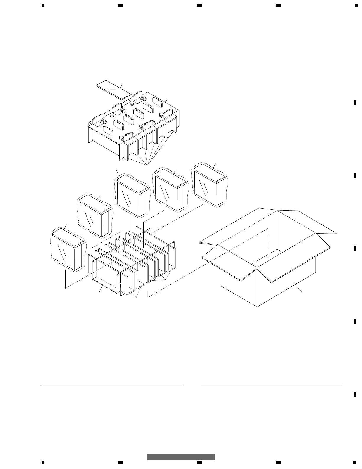
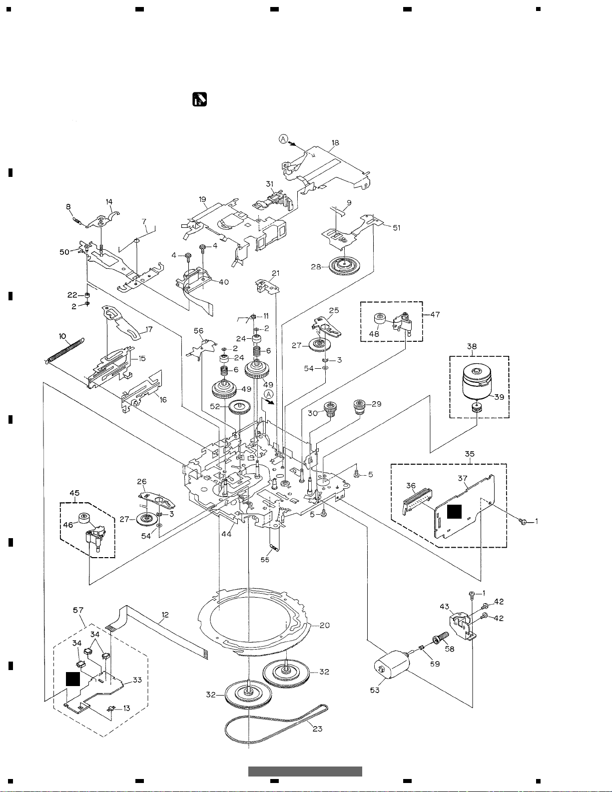
2. EXPLODED VIEWS AND PARTS LIST
2.1 PACKING
2
3
5
6
7
4
4
1
1
1
1
1
1 Polyethylene Bag CEG1042
2 Contain Box(M8027ZT) CHL4669
Contain Box(M8127ZT) CHL4670
3 Protector CHP2545
4 Protector CHP2544
5 Protector CHP2543
6 Protector CHP2542
7 Cover CEG1057
- PACKING SECTION PARTS LIST
Mark No. Description Part No.
Mark No. Description Part No.
NOTE:
- Parts marked by “*” are generally unavailable because they are not in our Master Spare Parts List.
- Screws adjacent to
∇ mark on the product are used for disassembly.
- For the applying amount of lubricants or glue, follow the instructions in this manual.
( In the case of no amount instructions, apply as you think it appropriate.)
Page 6
6
1
234
12
34
F
E
D
C
B
A
KEH-M8027ZT/XN/ES
2.2 EXTERIOR
Page 7

7
5
6
7
8
F
E
D
C
B
A
5
6
7
8
KEH-M8027ZT/XN/ES
1 Keyboard Unit CWM8359
2 LCD(LCD901) CAW1694
3 Connector(CN901) CKS4256
4 Holder CNC9543
5 Spacer CNM7828
6 Sheet CNM7880
7 Rubber CNV6820
8 Lighting Conductor CNV6821
9 Connector CNV7240
10 Grille Unit(M8027ZT) CXB7676
Grille Unit(M8127ZT) CXB7677
11 Knob Unit(VOL) CXB7678
12 Knob Unit(TUNE) CXB7679
13
Cassette Mechanism ModuleEXK4285
14 Screw ISS26P055FUC
15 Screw ASZ26P140FMC
16 Screw BMZ30P100FMC
17 Screw BSZ26P050FMC
18 Transistor(Q471,761) 2SB1185
19 Case CNB2754
20 Frame CNC9544
21 Earth CNC9555
* 22 Cushion CNM5281
23 Insulator CNM7401
24 Insulator CNM7436
25 Insulator CNM7437
26 Spacer CNM7755
27 Heat Sink CNR1613
28 Main Unit(M8027ZT) CWM8358
Main Unit(M8127ZT) CWM8360
29 Screw BMZ30P060FMC
30 Screw(M3x8) CBA1339
31 Plug(CN402) CKM1221
32 Connector(CN401) CKM1222
33 Connector(CN701) CKS3568
34 Connector(CN601) CKS4557
35 86146-48030(CN501) CKX1057
36 Holder CNC9545
37 Holder CNC9546
38
FM/AM Tuner Unit(M8027ZT)CWE1557
FM/AM Tuner Unit(M8127ZT)CWE1556
39 Holder CNC8855
40 Terminal(CN403) VNF1084
41 Terminal(CN404) VNF1084
42 Chassis Unit CXB7680
43 Screw BPZ20P060FMC
44 Button(SCAN) CAC7130
45 Button(AM)(M8027ZT) CAC7131
Button
(AM•FM)(M8127ZT)
CAC7134
46 Button(FM1•2)(M8027ZT) CAC7132
Button(SW1•2)(M8127ZT) CAC7135
47 Button(TAPE) CAC7133
48 Button(EJECT) CAC7136
49 Button(CD) CAC7137
50 Button( , ) CAC7138
51 Button(1-6) CAC7139
52 Door CAT2259
53 Spring CBH2538
54 Lighting Conductor CNV6817
55 Lighting Conductor CNV6818
56 Holder CNV6819
57 Lighting Conductor CNV6829
58 Holder CNV6976
59 Holder CNV7285
60 IC(IC201) TDA7384
- EXTERIOR SECTION PARTS LIST
Mark No. Description Part No.
Mark No. Description Part No.
Page 8
8
1
234
12
34
F
E
D
C
B
A
KEH-M8027ZT/XN/ES
2.2 CASSETTE MECHANISM MODULE
C
D
For grease application, refer to the service manual for CX-1011 (CRT2406).
Page 9

5
6
7
8
F
E
D
C
B
A
5
6
7
8
KEH-M8027ZT/XN/ES
9
Mark No. Description Part No. Mark No. Description Part No.
1 Screw BSZ20P040FMC
2 Washer CBF1037
3 Washer CBG1003
4 Screw EBA1028
5 Screw CBA1037
6 Spring EBH1653
7 Spring EBH1642
8 Spring EBH1641
9 Spring EBH1626
10 Spring EBH1627
11 Spring EBH1648
12 Cord EDD1024
13 Photo-reflector(Q101) EGN1004
14 Arm ENC1526
* 15 Lever ENC1544
16 Lever ENC1531
17 Arm ENC1532
18 Frame ENC1533
19 Holder ENC1534
20 Gear ENC1535
21 Arm ENC1550
22 Roller ENR1040
23 Belt ENT1027
24 Collar ENV1508
25 Arm ENV1539
26 Arm ENV1540
27 Gear ENV1569
28 Gear ENV1547
29 Gear ENV1560
30 Worm Wheel ENV1566
31 Lever ENV1551
32 Flywheel ENV1554
33 Gathering PCB ENX1073
34 Switch(S101,102,103) ESG1007
35 Deck Unit EWM1033
36 Plug(CN251) CKS3540
37 Gathering PCB ENX1067
38 Motor Unit(M1) EXA1491
39 Motor EXM1028
40 Head Assy(HD1) EXA1639
41 •••••
42 Screw BMZ20P022FMC
43 Bracket ENC1558
44 Chassis Unit EXA1615
45 Pinch Holder Unit EXA1608
46 Pinch Roller ENV1518
47 Pinch Holder Unit EXA1607
48 Pinch Roller ENV1518
49 Reel Unit EXA1625
50 Head Base Unit EXA1611
51 Lever Unit EXA1587
52 Gear Unit EXA1596
53 Motor Unit(M2) EXA1627
54 Washer HBF-179
55 Spring EBH1537
56 Arm ENC1537
57 Sensor Unit EWM1041
58 Worm Gear ENV1564
59 Spring EBH1545
- CASSETTE MECHANISM MODULE SECTION PARTS LIST
Page 10
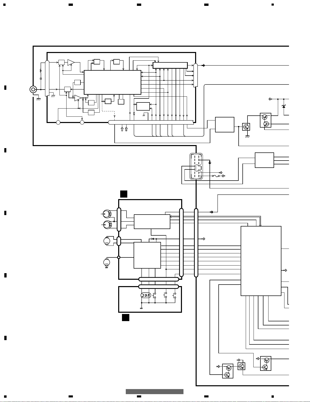
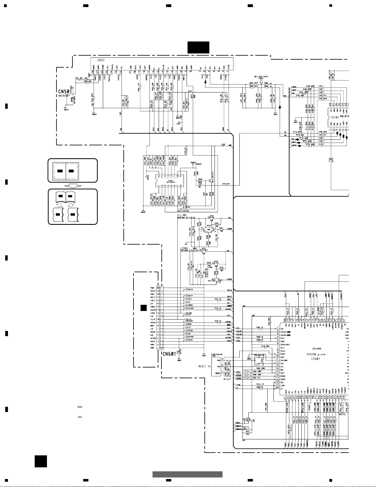
IC 721
HA12187FP
BUS IC
LDO
LDI
CSLOAD
MS
46
STBY
53
LCDPW
38
POWER
34
31
ENC1M
32
33
SYSTEM
CONTROLLER
IC 601(2/2)
PD5709B
LANLP
8
IPPW
15
CSEJ
ILMPW
B.U
CN701
CN402
Q761
B.U
Q752
Q753
FM/AM TUNER UNIT
19
3
PDIO
VCC
stby
B.U
LOAD
5
1
4
2
1
3
11
20
19
DECK UNIT
IC251
HA12228F
IC351
PA2020A
DOLBY-B
MECHANISM
DRIVER
CN251
CN252
CN254
CN255
CN253
6
16
MS
Lch
FWD
L-ch
REV
L-ch
39
32
33
18
19
17
3
15 6
8
7
10
CN256
3
15 6
S101
LOAD
S102
MODE
Q101
REEL
SENSE
M
M
M2
SUB
MOTOR
M1
MAIN
MOTOR
5
2
1
SENSOR UNIT
11
6
55
6
17
f/R
FR
42
41
DIR
MS
STBY
15
13
15
13
49
47
POS
ES
13
11
POS
ES
POS
ES
18
17
18
17
52
50
16
15
SC1
CM
20
B.U
16
16
51
14
SC2
SC1
CM
SC2
SC1
CM
SC2
VDD
CN501
ANT
S
63
SYSPW
PCE2
PCK
PCE1SLFMSD
S103
70µs
4
4
mtl
MTL
8
8
1
DIN1
2
DOUT
6
5
TXTX+
BUS+
BUS-
MUTE
Q482
AMB
AMPW
Q541
AUDIO 8
ST
B.U
BU
FU901
CSL
MTL
44
CSLOAD
Q762
74
SWVDPW
MUTE
LCD 8V
ILL 10V
Q751
B.U
AUDIO+B
24 25
ENC1P
ENC2M
ENC2P
MODE
37
36
35
IC 3
EEPROM
28
27
FM/AM 1ST IF 10.7MHz
T51 Q51 CF51
CF52 CF53
IC1
MIXER, IF AMP, DET.
6
21
18
LDET
COMP
222510 14 12 15 16 8 13 2 3 4
CF202
VDD
VCC
DI/DO
CE2CKCE1
SDBWSLFMSD
NL1
NL2
IC 2 FM MPX
AMANT
FMANT
ATT
ATT
AMRF
FMRF
IMG ADJ
RF ADJ
X901
10.25MHz
ANT ADJ
LOCL
23
LOCH
AMDET
MPXREF 41kHz
AM 2ND IF
450kHz
19
CREQ
11
DGND
1
STIND
L ch
5
R ch
924
AMDET
FMLOCL
20
177
AMPNS
WC
26
RFGND
AMIN
C
D
19
IC 541
HA12181FP
AM PNS
16
3
9
10
1
234
12
34
F
E
D
C
B
A
KEH-M8027ZT/XN/ES
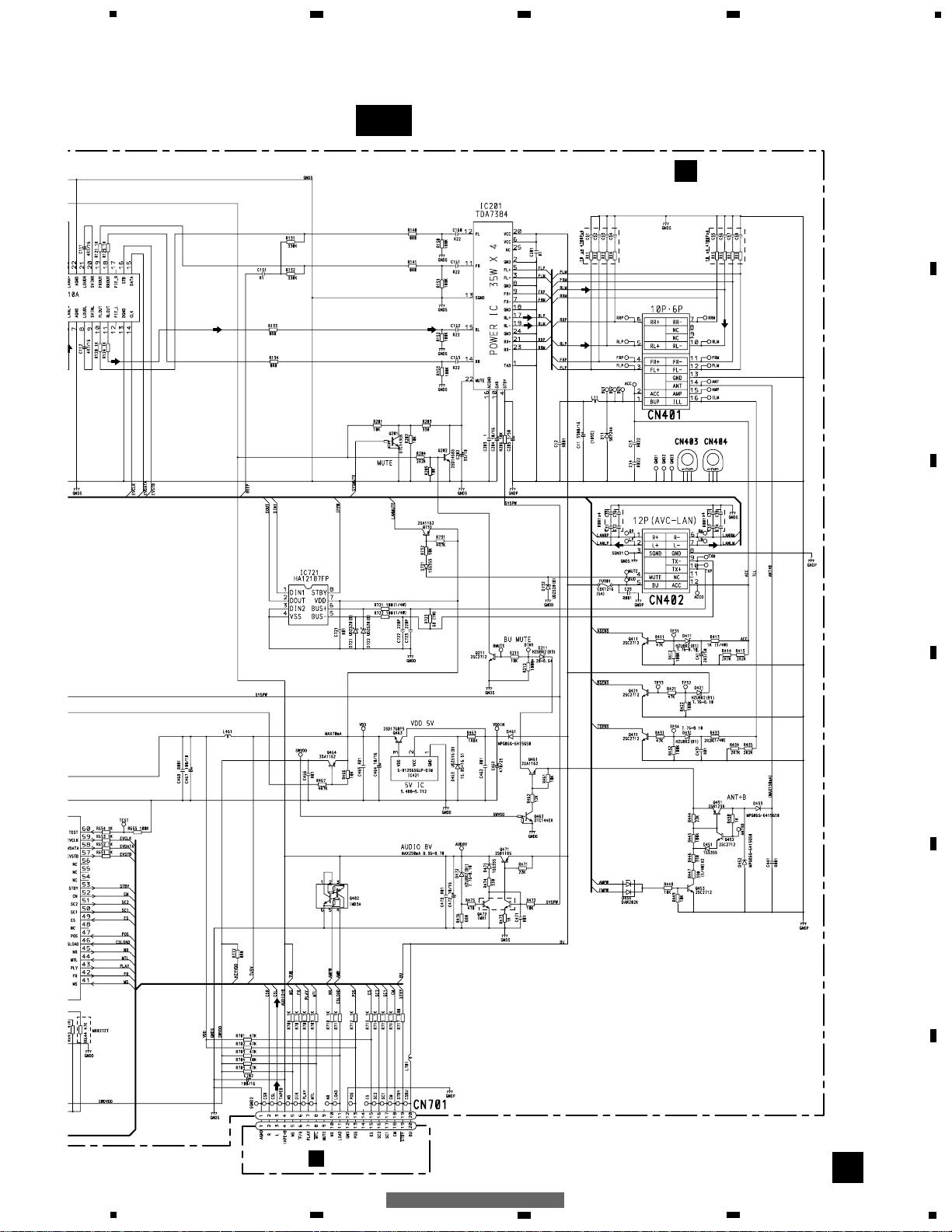
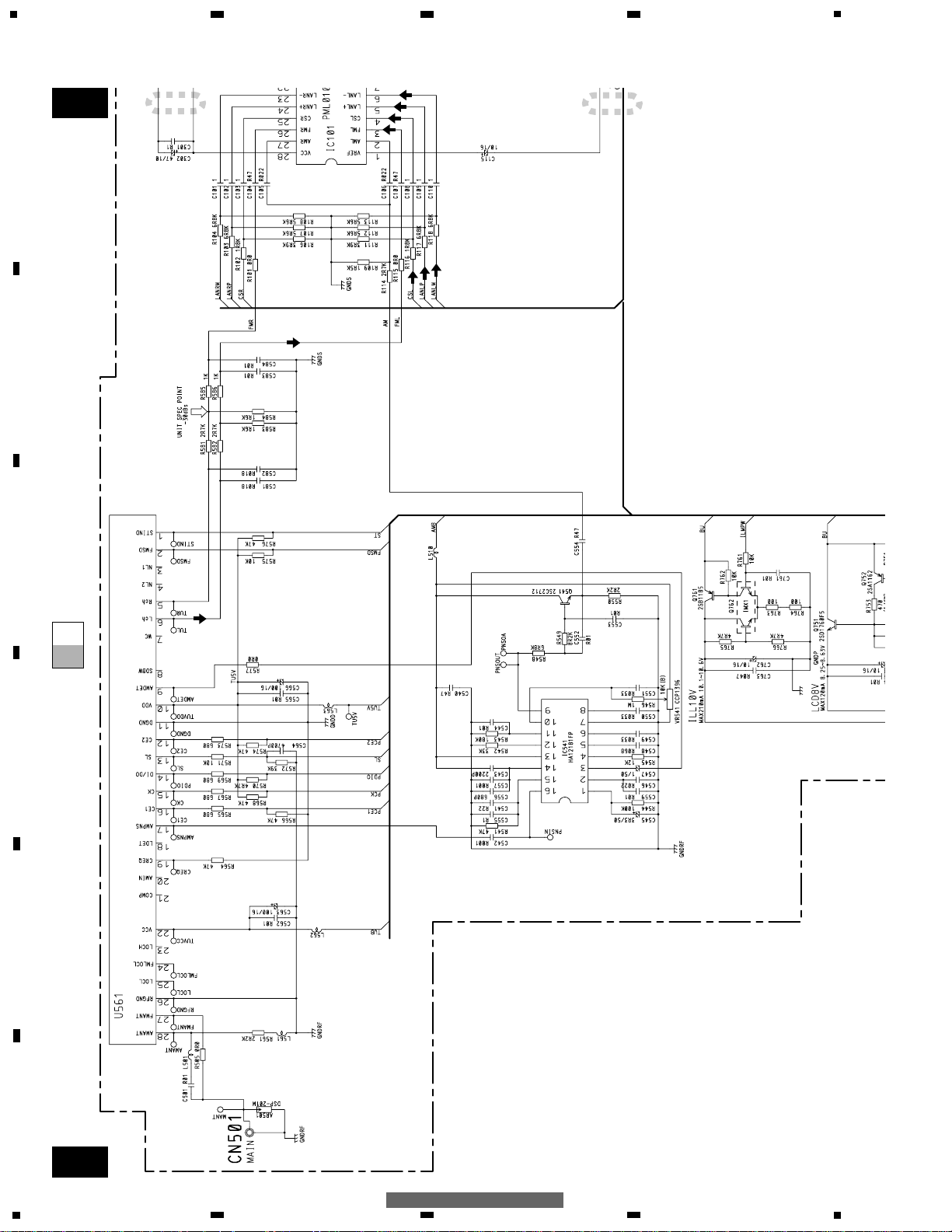
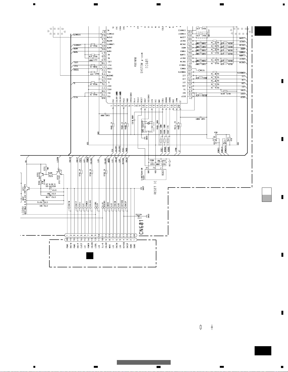
3. BLOCK DIAGRAM AND SCHEMATIC DIAGRAM
3.1 BLOCK DIAGRAM
Page 11
9
1
BSENS
ASENS
VDD
B.U
BACK UP
72
17
16
FMSD
SL
PCE1
PCK
PCE2
PDO
10
FLOUT
11
RLOUT
XOUT
XIN
B.U
SWVDD
IL+B
BL+B
ILL+B
CSEJ
ENC1M
ENC1P
LCDBL
5
3
19
17
RL—
RL+
FL+
FL-
GND
ISENS
5
76
FM L
3
POWER
7
LDO
34
LDI
31
ENC1M
32
14
LANL+
5
CSL
4
71
1
4
80
19
FL
12
RL
15
22
4
SYSTEM
CONTROLLER
RESET
POWER AMP
IC 101
PML010A
IC 681
S-80736AN-D0
IC 201
TDA7384
RESET
Q421
SYSPW
Q201
Q461
Q431
8
IPPW
IPPW
ELECTRONIC VOLUME/
SOURCE SELECTOR
STBY
MUTE
IC 901
LC75853NE
LCD DRIVER
KEY MATRIX
LCD
10
16
5
15
17
19
12
11
16
6
4
2
9
5
LDI
LDO
KEY DATA
LCD DATA
64
61
CN601
CN901
KEYBOARD UNIT
MAIN UNIT
10
X601
12
ACC
RL—
RL+
ILL
FL—
FL+
2
CN401
IC 601(1/2)
PD5709B
Q411
Q462
ST
20
Q211
B.U
SYSPW
63
Q731
23
1
DIN1
TX
22
2
DOUT
RX1
LANMUTE
65
AMPW
66
AMPW
AUDIO 8V
ILL
Q202
VDD 5V
IC 421
S-81256SGUP-DIM
Q463
3
Q464
74
LANMUTE
MUTE
SWVDD
MUTE
SYSMUTE
62
BU MUTE
2
B.U
Q471
B.U
Q472
SYSPW
BSENS
ASENS
ISENS
19
FROUT
FR
11
BEEP
21
BACK UP
D901-D931
S914
EJECT
MAIN VOLUME
VR901
MODE SELECTOR
VR902
POWER
ENC1M
ENC1P
POWER
ENC1P
ENC2M
ENC2P
13
8
3
6
18
15
MODE
ENC2M
ENC2P
MODE
A
B
PDI
79
Q453
ANT+B
ANT
ANT
ACC
FMPW
67
AMPW
66
Q452
Q451
D454
2
AML
B.U
11
5
6
7
8
F
E
D
C
B
A
5
6
7
8
KEH-M8027ZT/XN/ES
Page 12
A-a A-b
A-a
A-b
A-b
A-a
Large size
SCH diagram
Guide page
Detailed page
Note: When ordering service parts, be sure to refer to " EXPLODED VIEWS AND PARTS LIST" or
"ELECTRICAL PARTS LIST".
A-a
A
B
CN901
FM/AM TUNER UNIT
Decimal points for resistor
and capacitor fixed values
are expressed as :
2.2 2R2
0.022 R022
←
The > mark found on some component parts indicates
the importance of the safety factor of the part.
Therefore, when replacing, be sure to use parts of
identical designation.
Symbol indicates a resistor.
No differentiation is made between chip resistors and
discrete resistors.
NOTE :
Symbol indicates a capacitor.
No differentiation is made between chip capacitors and
discrete capacitors.
AM PNS
FM(30%): -30dBs
AM(30%):-12.7dBs
FM(30%): -30dBs
AM(30%):-21.7dBs
TAPE:-11.8dBs
CD: +1.0dBs
12
1
234
12
34
F
E
D
C
B
A
KEH-M8027ZT/XN/ES
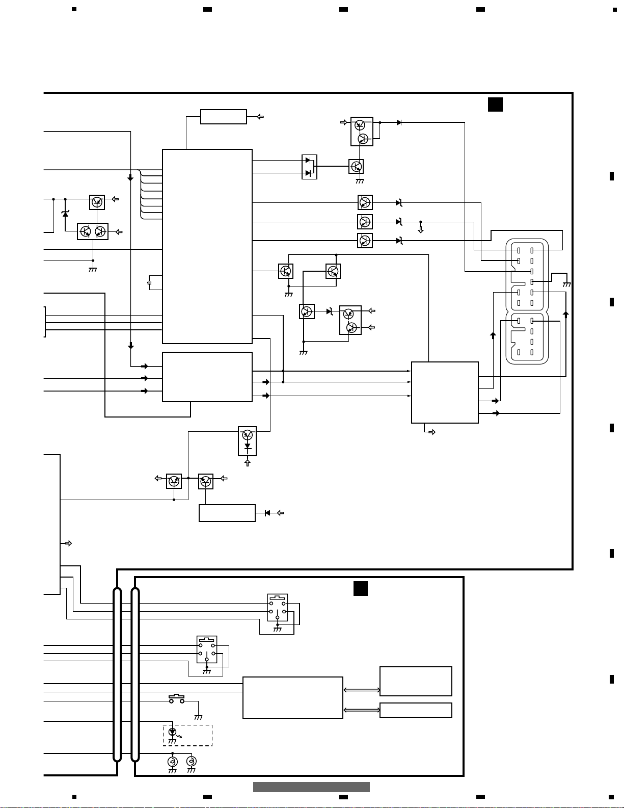
3.2 OVERALL CONNECTION DIAGRAM(GUIDE PAGE
Page 13
A-b
A
A
C
CN251
MAIN UNIT
>
ACC SENSE
B.UP SENSE
ILM SENSE
LAN MUTE
BUS IC
E-VOL
FM(30%):-12.9dBs
AM(30%):-12.7dBs
TAPE: +0.3dBs
CD: +7.1dBs
FM(30%):+12.6dBs
AM(30%):+13.3dBs
TAPE:+26.3dBs
CD:+33.1dBs
TAPE:-8.4dBs
(400Hz 200nWb/m)
CD:+8.2dBs
(1KHz 0dB)
13
5
6
7
8
F
E
D
C
B
A
5
6
7
8
KEH-M8027ZT/XN/ES
Page 14
14
1
234
12
34
F
E
D
C
B
A
KEH-M8027ZT/XN/ES
A-a
A-b
A-a
A-a
A-b
1
2
FM/AM TUNER UNIT
AM PNS
FM(30%): -30dBs
AM(30%):-12.7dBs
FM(30%): -30dBs
AM(30%):-21.7dBs
TAPE:-11.8dBs
CD: +1.0dBs
Page 15
A-a
A-b
A-a
A-a
A-b
3 4
B
CN901
Decimal points for resistor
and capacitor fixed values
are expressed as :
2.2 2R2
0.022 R022
←
The > mark found on some component parts indicates
the importance of the safety factor of the part.
Therefore, when replacing, be sure to use parts of
identical designation.
Symbol indicates a resistor.
No differentiation is made between chip resistors and
discrete resistors.
NOTE :
Symbol indicates a capacitor.
No differentiation is made between chip capacitors and
discrete capacitors.
15
5
6
7
8
F
E
D
C
B
A
5
6
7
8
KEH-M8027ZT/XN/ES
Page 16

16
1
234
12
34
F
E
D
C
B
A
KEH-M8027ZT/XN/ES
A-a
A-b
A-b
1
2
A
MAIN UNIT
>
ACC SENSE
LAN MUTE
BUS IC
E-VOL
FM(30%):-12.9dBs
AM(30%):-12.7dBs
TAPE: +0.3dBs
CD: +7.1dBs
FM(30%):+12.6dBs
AM(30%):+13.3dBs
TAPE:+26.3dBs
CD:+33.1dBs
CD:+8.2dBs
(1KHz 0dB)
Page 17

A-a
A-b
A-b
3 4
C
CN251
ACC SENSE
B.UP SENSE
ILM SENSE
TAPE:-8.4dBs
(400Hz 200nWb/m)
17
5
6
7
8
F
E
D
C
B
A
5
6
7
8
KEH-M8027ZT/XN/ES
Page 18

18
1
234
12
34
F
E
D
C
B
A
KEH-M8027ZT/XN/ES
60mA, 8V
B
A
KEYBOARD UNIT
CN601
B
3.3 KEYBOARD UNIT
Page 19

19
5
6
7
8
F
E
D
C
B
A
5
6
7
8
KEH-M8027ZT/XN/ES
Page 20

20
1
234
1
2
34
F
E
D
C
B
A
KEH-M8027ZT/XN/ES
3.4 CASSETTE MECHANISM MODULE
C
A
C
CN701
DECK UNIT
MUTE
HA12228F
11
12
13
14
15
16
17
18
19
20
40
39
38
37
36
35
34
33
32
31
30
292827
26
252423
22
21
1
234
5
678
9
10
C253
390P
C251
C256
R01
C405
R03
R404
270K
R01
C404
910
R403
3R3K
C255
R01
C272
R1
C401
3900P
HD1
HEAD ASSY
EXA1639
TEST TAPE
NCT-150
(400Hz, 200nWb/m)
RL
RR
FR
FL
C302
R1
C301
R1
VR301
33K(B)
-8.24dBs±1dB
Fwd-R
Fwd-L
Rev-R
Rev-L
NF1(R)
Vref1
RIN(L)
NC
RIN(R)
GND
FIN(R)
Vref2
FIN(L)
NFI(L)
M-OUT(L)
EQOUT(L)
Vref4
TAI(L)
BIAS
NC
DET(L)
MSGV(S)
MUTE
120/70
ser/REP
f/R
MSDET
MSI
MAOUT
MSGV(R)
MOUT(R)
EQOUT(R)
Vref3
TAI(R)
RIP
PBOUT(R)
NC
DET(R)
NR
CN252
CN251
Dolby-B NR
IC251
390P
C252
390P
C254
390P
PBOUT(L)
NC
VCC
MSOUT
NC
C403
R402
R33
C402
15K
R401
18K
R271
C271
1/50
C310
R1
C309
R1
CCP1280
VR302
33K(B)
CCP1280
0R0
R410
0R0
R408
0R0
R407
0R0
R406
R409
0R0
R411
Page 21

21
5
6
7
8
F
E
D
C
B
A
5
6
7
8
KEH-M8027ZT/XN/ES
D
C
D
CN701
SENSOR UNIT
C405
R033
270K
R351 1K
R352 1K
R353 1K
R354 1K
R373 0R0
R355 270K
C352
3900P
R362 300
C351 R22
C353 R01
C354 R01
R374 0R0
C356 R01
C355 R1
D352 1SS355
M1 MOTOR UNIT
(MAIN MOTOR)
EXA1491
S101
LOAD
ESG1007
S102
ESG1007
MODE
REEL SENSE
Q101
EGN1004
M2
MOTOR UNIT
(SUB MOTOR)
EXA1627
RS3
RS2
RS1
SC2
SC1
TAB
MC
CE
VCC2
NC
VCC
MCS
RRS
FRS
RSB
C
TAB
MS2
NC
NC
MM
SM1
RSB
GND
RS
mtl
MCS
load
CN255
CN253
CN256
CN254
MECHANISM
DRIVER
IC351 PA2020A
C403
R022
S103
ESG1007
70µs
R375
0R0
SWITCH POSITION:
SENSOR UNIT
S101:LOAD SWITCH..........EJECT-PLAY
S102:MODE SWITCH............ON-OFF
S103:70µs SWITCH...............ON-OFF
The underlined indicates the switch position.
0R0
R409
L101
L102
Page 22

Capacitor
Connector
P.C.Board
Chip Part
A
A
MAIN UNIT
SIDE B
SIDE A
NOTE FOR PCB DIAGRAMS
1.The parts mounted on this PCB
include all necessary parts for
several destination.
For further information for
respective destinations, be sure
to check with the schematic dia gram.
2.Viewpoint of PCB diagrams
FM/AM TUNER UNIT
ANTENNA
22
1
234
12
34
F
E
D
C
B
A
KEH-M8027ZT/XN/ES
4. PCB CONNECTION DIAGRAM
4.1 MAIN UNIT
Page 23

A
SIDE A
FRONT
C
CN251
B
CN901
23
5
6
7
8
F
E
D
C
B
A
5
6
7
8
KEH-M8027ZT/XN/ES
Page 24

24
1
234
12
34
F
E
D
C
B
A
KEH-M8027ZT/XN/ES
A
A
MAIN UNIT
Page 25

A
SIDE B
25
5
6
7
8
F
E
D
C
B
A
5
6
7
8
KEH-M8027ZT/XN/ES
Page 26

B
B
KEYBOARD UNIT
B
KEYBOARD UNIT
SIDE A
SIDE B
MODE SELECTOR
TAPE
FM1 2
AM
.
CD
6
5
4
3
2
1
EJECT
UP
DOWN
SCAN
MAIN VOLUME
A
CN601
26
1
234
12
34
F
E
D
C
B
A
KEH-M8027ZT/XN/ES
4.2 KEYBOARD UNIT
Page 27

27
5
6
7
8
F
E
D
C
B
A
5
6
7
8
KEH-M8027ZT/XN/ES
4.3 DECK UNIT
C
C
DECK UNIT
C
DECK UNIT
SIDE A
SIDE B
CN251
C271
IC,Q
IC251
Q351
Q352
ADJ
VR302
VR301
IC351
CN252
CN254
CN253
CN255
M1
M2
HEAD ASSY
21
22
A
CN701
D
CN256
Page 28
28
1
234
12
34
F
E
D
C
B
A
KEH-M8027ZT/XN/ES
4.4 SENSOR UNIT
D
D
SENSOR UNIT
1
2
3
4
5
6
S101
LOAD
S102
MODE
S103
70µs
CN256
Q101
REEL SENSE
L101
L102
C
CN253
Page 29

5
6
7
8
F
E
D
C
B
A
5
6
7
8
KEH-M8027ZT/XN/ES
29
5. ELECTRICAL PARTS LIST
NOTES:
- Parts whose parts numbers are omitted are subject to being not supplied.
- The part numbers shown below indicate chip components.
Chip Resistor
RS1/_S___J,RS1/__S___J
Chip Capacitor (except for CQS.....)
CKS....., CCS....., CSZS.....
=====Circuit Symbol and No.===Part Name Part No.
--- ------ ------------------------------------------ -------------------------
Unit Number : CWM8358 (M8027ZT)
Unit Number : CWM8360 (M8127ZT)
Unit Name : Main Unit
MISCELLANEOUS
IC 101 IC PML010A
IC 201 IC TDA7384
IC 421 IC
S-81256SGUP-DIM
IC 541 IC HA12181FP
IC 601 IC PD5709B
IC 681 IC S-80736AN-D0
IC 721 IC HA12187FP
Q 201 Transistor DTC143EK
Q 202 Transistor 2SD1468S
Q 211 Chip Transistor 2SC2712
Q 411 Chip Transistor 2SC2712
Q 421 Chip Transistor 2SC2712
Q 431 Chip Transistor 2SC2712
Q 451 Transistor 2SB1238
Q 452 Chip Transistor 2SC2712
Q 453 Chip Transistor 2SC2712
Q 461 Transistor 2SA1162
Q 462 Transistor DTC144EK
Q 463 Transistor 2SD1760F5
Q 464 Transistor 2SA1162
Q 471 Transistor 2SB1185
Q 472 Transistor IMX1
Q 482 Transistor IMD3A
Q 541 Chip Transistor 2SC2712
Q 731 Transistor 2SA1162
Q 751 Transistor 2SD1760F5
Q 752 Transistor 2SA1162
Q 753 Transistor DTC114EK
Q 761 Transistor 2SB1185
Q 762 Transistor IMX1
D 11 Diode 5KP24A
D 211 Diode HZU8R2(B3)
D 411 Diode HZU8R2(B1)
D 421 Diode HZU8R2(B1)
D 431 Diode HZU8R2(B1)
D 451 Diode 1SS355
D 452 Diode MPG06G-6415G50
D 453 Diode MPG06G-6415G50
D 454 Diode DAN202K
D 461 Diode MPG06G-6415G50
D 463 Diode UDZS16(B)
D 471 Diode 1SS355
D 472 Diode HZU8R2(B1)
D 721 Diode UDZS20(B)
D 722 Diode UDZS20(B)
D 731 Diode 1SS355
D 732 Diode UDZS20(B)
D 751 Diode UDZS9R1(B)
L 11 Choke Coil 600µH CTH1225
L 461 Ferri-Inductor LAU150K
L 501 Ferri-Inductor LAU2R2K
L 510 Inductor LCTA101J2520
L 561 Coil CTB1103
L 562 Inductor LCTA1R0J2520
L 563 Inductor LAU1R0K
L 701 Inductor LFEA4R7J
X 601 Radiator 10.00MHz CSS1428
VR 541 10kΩ(B) CCP1396
FU 901 Fuse 5A CEK1216
AR 501 Surge Protector DSP-201M
FM/AM Tuner Unit(M8027ZT) CWE1557
FM/AM Tuner Unit(M8127ZT) CWE1556
RESISTORS
R 11 RS1/16S100J
R 12 RS1/16S100J
R 13 RS1/16S100J
R 14 RS1/16S100J
R 15 RS1/16S100J
R 16 RS1/16S100J
R 17 RS1/16S100J
R 18 RS1/16S100J
R 101 RS1/16S0R0J
R 102 RS1/16S182J
R 103 RS1/16S682J
R 104 RS1/16S682J
R 106 RS1/16S392J
R 107 RS1/16S562J
R 108 RS1/16S562J
R 109 RS1/16S152J
R 111 RS1/16S392J
R 112 RS1/16S562J
R 113 RS1/16S562J
R 114 RS1/16S272J
R 115 RS1/16S0R0J
R 116 RS1/16S182J
R 117 RS1/16S682J
R 118 RS1/16S682J
R 120 RS1/16S102J
R 121 RS1/16S102J
R 124 RS1/16S102J
R 125 RS1/16S102J
R 131 RS1/16S334J
R 132 RS1/16S334J
R 133 RS1/16S0R0J
R 134 RS1/16S0R0J
R 140 RS1/16S0R0J
R 141 RS1/16S0R0J
R 150 RS1/16S104J
R 151 RS1/16S104J
R 152 RS1/16S104J
R 153 RS1/16S104J
R 201 RS1/16S103J
R 202 RS1/16S103J
=====Circuit Symbol and No.===Part Name Part No.
--- ------ ------------------------------------------ -------------------------
A
Page 30

30
1
234
12
34
F
E
D
C
B
A
KEH-M8027ZT/XN/ES
R 203 RS1/16S331J
R 204 RS1/16S222J
R 205 RS1/16S103J
R 206 RS1/16S103J
R 211 RS1/16S183J
R 212 RS1/16S104J
R 411 RS1/16S473J
R 412 RS1/16S104J
R 413 RD1/4PU102J
R 414 RS1/10S272J
R 415 RS1/10S222J
R 421 RS1/16S473J
R 422 RS1/16S104J
R 431 RS1/16S473J
R 432 RS1/16S104J
R 433 RD1/4PU222J
R 434 RS1/10S272J
R 435 RS1/10S222J
R 444 RS1/16S223J
R 445 RS1/16S104J
R 446 RD1/4PU391J
R 447 RD1/4PU391J
R 448 RS1/16S103J
R 449 RS1/16S103J
R 450 RS1/16S102J
R 461 RS1/16S103J
R 462 RS1/16S123J
R 463 RS1/16S182J
R 466 RS1/16S103J
R 467 RS1/16S472J
R 471 RS1/16S223J
R 472 RS1/16S103J
R 473 RS1/16S102J
R 474 RS1/16S331J
R 475 RS1/16S471J
R 476 RS1/16S681J
R 505 RS1/16S0R0J
R 541 RS1/16S473J
R 542 RS1/16S333J
R 543 RS1/16S184J
R 544 RS1/16S104J
R 545 RS1/16S123J
R 546 RS1/16S105J
R 548 RS1/16S682J
R 549 RS1/16S822J
R 550 RS1/16S222J
R 561 RS1/16S222J
R 564 RS1/16S473J
R 565 RS1/16S681J
R 566 RS1/16S473J
R 567 RS1/16S681J
R 568 RS1/16S473J
R 569 RS1/16S681J
R 570 RS1/16S472J
R 571 RS1/16S103J
R 572 RS1/16S393J
R 573 RS1/16S681J
R 574 RS1/16S473J
R 575 RS1/16S103J
R 576 RS1/16S473J
R 577 RS1/16S0R0J
R 581 RS1/16S272J
R 582 RS1/16S272J
R 583 RS1/16S162J
R 584 RS1/16S162J
R 585 RS1/16S102J
R 586 RS1/16S102J
R 601 RS1/16S102J
R 602 RS1/16S102J
R 603 RS1/16S102J
R 604 RS1/16S104J
R 605 RS1/16S104J
R 606 RS1/16S104J
R 607 RS1/16S473J
R 608 RS1/16S102J
R 609 RS1/16S102J
R 610 RS1/16S473J
R 611 RS1/16S473J
R 612 RS1/16S102J
R 615 RS1/16S472J
R 616 RS1/16S102J
R 617 RS1/16S102J
R 618 RS1/16S102J
R 619 RS1/16S102J
R 620 RS1/16S102J
R 623 RS1/16S102J
R 624 RS1/16S473J
R 625 RS1/16S102J
R 626 RS1/16S473J
R 627 RS1/16S102J
R 628 RS1/16S473J
R 629 RS1/16S102J
R 630 RS1/16S473J
R 631 RS1/16S102J
R 632 RS1/16S473J
R 633 RS1/16S102J
R 634 RS1/16S473J
R 641 (M8127ZT) RS1/16S473J
R 644 (M8027ZT) RS1/16S473J
R 651 RS1/16S102J
R 652 RS1/16S102J
R 653 RS1/16S102J
R 654 RS1/16S102J
R 655 RS1/16S104J
R 661 RS1/16S102J
R 662 RS1/16S473J
R 663 RS1/16S473J
R 664 RS1/16S102J
R 665 RS1/16S102J
R 671 RS1/16S473J
R 673 RS1/16S473J
R 681 RS1/16S104J
R 701 RS1/16S473J
R 702 RS1/16S473J
R 703 RS1/16S473J
R 704 RS1/16S103J
R 705 RS1/16S473J
R 706 RS1/16S102J
R 707 RS1/16S102J
R 708 RS1/16S102J
R 709 RS1/16S102J
R 710 RS1/16S102J
R 711 RS1/16S102J
R 712 RS1/16S102J
R 713 RS1/16S102J
R 714 RS1/16S102J
R 715 RS1/16S102J
R 716 RS1/16S102J
R 717 RS1/16S681J
R 721 RD1/4PU101J
R 722 RD1/4PU101J
R 723 RS1PMF680J
R 731 RS1/16S472J
R 732 RS1/16S103J
R 741 RS1/16S102J
R 744 RS1/16S102J
R 745 RS1/16S102J
R 751 RS1/16S103J
R 752 RS1/16S472J
R 753 RD1/4PU471J
=====Circuit Symbol and No.===Part Name Part No.
--- ------ ------------------------------------------ -------------------------
=====Circuit Symbol and No.===Part Name Part No.
--- ------ ------------------------------------------ -------------------------
Page 31

5
6
7
8
F
E
D
C
B
A
5
6
7
8
KEH-M8027ZT/XN/ES
31
R 761 RS1/16S103J
R 762 RS1/16S103J
R 763 RS1/16S101J
R 764 RS1/16S101J
R 765 RS1/16S472J
R 766 RS1/16S472J
R 772 RS1/16S0R0J
CAPACITORS
C 11 3300µF/16V CCH1177
C 12 CKSQYB102K50
C 14 CKSRYB223K50
C 15 CKSRYB223K50
C 31 CKSRYB102K50
C 32 CKSRYB102K50
C 33 CKSRYB102K50
C 34 CKSRYB102K50
C 35 CKSRYB102K50
C 36 CKSRYB102K50
C 37 CKSRYB102K50
C 38 CKSRYB102K50
C 39 CKSQYB102K50
C 51 CKSRYB472K50
C 52 CKSRYB472K50
C 53 CKSRYB472K50
C 54 CKSRYB472K50
C 55 CKSRYB472K50
C 56 CKSRYB472K50
C 57 CKSRYB472K50
C 58 CKSRYB472K50
C 101 CKSRYF105Z10
C 102 CKSRYF105Z10
C 103 CKSRYF105Z10
C 104 CKSRYF474Z16
C 105 CKSRYB223K50
C 106 CKSRYB223K50
C 107 CKSRYF474Z16
C 108 CKSRYF105Z10
C 109 CKSRYF105Z10
C 110 CKSRYF105Z10
C 111 CEJQNP4R7M16
C 112 CEJQNP4R7M16
C 115 CEJQ100M16
C 151 CKSRYB104K16
C 160 CFTNA224J50
C 161 CFTNA224J50
C 162 CFTNA224J50
C 163 CFTNA224J50
C 201 CKSQYB104K50
C 202 CEJQ330M10
C 203 CFTNA105J50
C 204 CEJQ100M16
C 205 CEJQ1R0M50
C 301 CKSRYB104K16
C 302 CEJQ470M10
C 411 CEJQ2R2M50
C 431 CKSQYB103K50
C 441 CKSQYB102K50
C 461 CEAT471M25
C 462 CKSRYB103K50
C 464 CEJQ100M16
C 465 CKSRYB103K50
C 466 CKSRYB103K50
C 467 CEJQ101M10
C 468 CKSRYB102K50
C 471 CKSRYB103K50
C 472 CEJQ100M16
C 473 CKSRYB103K50
C 501 CKSQYB103K50
C 540 CKSRYF474Z16
C 541 CKSRYF224Z16
C 542 CKSRYB102K50
C 543 CKSRYB222K50
C 544 CKSRYB103K50
C 545 CEJQ3R3M50
C 546 CKSRYB223K50
C 547 CEJQ1R0M50
C 548 CQMA683J50
C 549 CQMA333J50
C 550 CQMA333J50
C 551 CQMA333J50
C 552 CKSRYB103K50
C 553 CKSRYB103K50
C 554 CKSRYF474Z16
C 555 CKSRYB104K16
C 556 CKSRYB681K50
C 557 CKSRYB102K50
C 559 CKSRYB103K50
C 562 CKSRYB103K50
C 563 CEJQ101M16
C 564 CKSRYB472K50
C 565 CKSRYB103K50
C 566 CEJQ101M16
C 581 CKSRYB183K50
C 582 CKSRYB183K50
C 583 CKSRYB103K50
C 584 CKSRYB103K50
C 601 CKSRYB102K50
C 602 CKSRYB102K50
C 603 CCSRCH101J50
C 604 CCSRCH101J50
C 605 CCSRCH101J50
C 606 CCSRCH101J50
C 607 CCSRCH101J50
C 608 CCSRCH101J50
C 610 CKSRYB102K50
C 611 CKSRYB102K50
C 681 CKSRYB103K50
C 682 CKSRYB223K50
C 702 CEJQ101M16
C 721 CKSRYB103K50
C 722 CKSQYB221K50
C 723 CKSQYB221K50
C 751 CKSRYB103K50
C 752 CEJQ1R0M50
C 753 CEJQ100M16
C 754 CKSRYB103K50
C 761 CKSRYB103K50
C 762 CEJQ100M16
C 763 CKSRYB473K50
C 771 CEJQ4R7M35
Unit Number : CWM8359
Unit Name : Keyboard Unit
MISCELLANEOUS
IC 901 IC LC75853NE
D 901 Chip LED SML210FC(KL)
D 902 Chip LED SML210FC(KL)
D 903 Chip LED SML210FC(KL)
D 904 Chip LED SML210FC(KL)
D 905 Chip LED SML210FC(KL)
D 906 Chip LED SML210FC(KL)
D 907 Chip LED SML210FC(KL)
D 908 Chip LED SML210FC(KL)
D 909 Chip LED SML210FC(KL)
=====Circuit Symbol and No.===Part Name Part No.
--- ------ ------------------------------------------ -------------------------
=====Circuit Symbol and No.===Part Name Part No.
--- ------ ------------------------------------------ -------------------------
B
Page 32

32
1
234
12
34
F
E
D
C
B
A
KEH-M8027ZT/XN/ES
D 910 Chip LED SML210FC(KL)
D 911 Chip LED SML210FC(KL)
D 912 Chip LED SML210FC(KL)
D 913 Chip LED SML210FC(KL)
D 914 Chip LED SML210FC(KL)
D 915 Chip LED SML210FC(KL)
D 916 Chip LED SML210FC(KL)
D 917 Chip LED SML210FC(KL)
D 918 Chip LED SML210FC(KL)
D 919 Chip LED SML210FC(KL)
D 920 Chip LED SML210FC(KL)
D 921 Chip LED SML210FC(KL)
D 922 Chip LED SML210FC(KL)
D 923 Chip LED SML210FC(KL)
D 924 Chip LED SML210FC(KL)
D 925 Chip LED SML210FC(KL)
D 926 Chip LED SML210FC(KL)
D 928 Chip LED SML210FC(KL)
D 929 Chip LED SML210FC(KL)
D 930 Chip LED SML210FC(KL)
D 931 Chip LED SML210FC(KL)
D 951 Diode 1SS355
D 952 Diode 1SS355
D 953 Diode 1SS355
D 954 Diode 1SS355
L 906 Inductor CTF1384
L 907 Inductor CTF1384
L 908 Inductor CTF1384
L 909 Inductor CTF1384
IL 901 Lamp 60mA,8V CEL1710
IL 902 Lamp 60mA,8V CEL1710
VR 901 Encoder Switch(MAIN VOLUME) CSD1048
VR 902 Encoder Switch(MODE SELECTOR) CSD1067
LCD 901 LCD CAW1694
RESISTORS
R 901 RS1/16S103J
R 902 RS1/16S683J
R 911 RS1/16S820J
R 912 RS1/16S101J
R 913 RS1/16S820J
R 914 RS1/16S101J
R 915 RS1/16S820J
R 916 RS1/16S101J
R 917 RS1/16S820J
R 918 RS1/16S101J
R 919 RS1/16S820J
R 920 RS1/16S101J
R 921 RS1/16S820J
R 922 RS1/16S101J
R 923 RS1/16S820J
R 924 RS1/16S101J
R 925 RS1/16S820J
R 926 RS1/16S101J
R 927 RS1/16S101J
R 928 RS1/16S101J
R 929 RS1/16S101J
R 930 RS1/16S101J
R 931 RS1/16S101J
R 932 RS1/16S101J
R 933 RS1/16S101J
R 934 RS1/16S101J
R 935 RS1/16S101J
R 941 RS1/16S6R8J
R 942 RS1/16S6R8J
R 943 RS1/16S3R9J
R 944 RS1/16S3R9J
R 945 RS1/16S6R8J
R 946 RS1/16S6R8J
R 947 RS1/16S3R9J
R 948 RS1/16S3R9J
CAPACITORS
C 901 CKSRYB821K50
C 902 CKSRYB473K50
C 903 CKSRYB473K50
C 904 CKSRYB103K50
C 906 CKSRYB102K50
C 907 CKSRYB102K50
C 908 CKSRYB102K50
C 909 CKSRYB102K50
Unit Number : EWM1033
Unit Name : Deck Unit
MISCELLANEOUS
IC 251 IC HA12228F
IC 351 IC PA2020A
D 352 Diode 1SS355
VR 301 Semi-fixed 33kΩ(B) CCP1280
VR 302 Semi-fixed 33kΩ(B) CCP1280
RESISTORS
R 271 RS1/16S183J
R 285 RS1/16S0R0J
R 351 RS1/16S102J
R 352 RS1/16S102J
R 353 RS1/16S102J
R 354 RS1/16S102J
R 355 RS1/16S274J
R 362 RS1/8S301J
R 373 RS1/16S0R0J
R 374 RS1/8S0R0J
R 375 RS1/8S0R0J
R 401 RS1/16S153J
R 402 RS1/16S332J
R 403 RS1/16S911J
R 404 RS1/16S274J
CAPACITORS
C 251 CKSRYB391K50
C 252 CKSRYB391K50
C 253 CKSRYB391K50
C 254 CKSRYB391K50
C 255 CKSRYB103K50
C 256 CKSRYB103K50
C 271 1µF/50V ECH0002
C 272 CKSRYB104K16
C 301 CKSRYB104K16
C 302 CKSRYB104K16
C 309 CKSRYB104K16
C 310 CKSRYB104K16
C 351 CKSQYB224K25
C 352 CKSRYB392K50
C 353 CKSRYB103K50
C 354 CKSRYB103K50
C 355 CKSQYB104K50
C 356 CKSRYB103K50
C 401 CKSRYB392K50
C 402 CKSRYB334K10
C 403 CKSRYB223K25
C 404 CKSRYB103K50
C 405 CKSRYB333K16
=====Circuit Symbol and No.===Part Name Part No.
--- ------ ------------------------------------------ -------------------------
=====Circuit Symbol and No.===Part Name Part No.
--- ------ ------------------------------------------ -------------------------
C
Page 33

33
5
6
7
8
F
E
D
C
B
A
5
6
7
8
KEH-M8027ZT/XN/ES
Unit Number : EWM1041
Unit Name : Sensor Unit
MISCELLANEOUS
S 101 Switch(LOAD) ESG1007
S 102 Switch(MODE) ESG1007
S 103 Switch(70µs) ESG1007
Q 101 Photo-reflector EGN1004
L 101 Inductor CTF1546
L 102 Inductor CTF1546
Miscellaneous Parts List
M 1 Motor Unit(MAIN) EXA1491
M 2 Motor Unit(SUB) EXA1627
HD 1 Head Assy EXA1639
=====Circuit Symbol and No.===Part Name Part No.
--- ------ ------------------------------------------ -------------------------
D
Page 34

34
1
234
12
34
F
E
D
C
B
A
KEH-M8027ZT/XN/ES
6. ADJUSTMENT
6.1 CASSETTE MECHANISM ADJUSTMENT
MAIN UNIT
FM/AM TUNER UNIT
DECK UNIT
VR302
mV
Meter(2)
VR301
L-CH
R-CH
Pin2
Pin3
CN251
DECK UNIT
Extension Cord GGD1121
DOLBY B NR ADJUSTMENT
No. Test Tape Adjustment Point Adjustment Method
(Switch Position)
1 NCT-150 VR301(Lch),VR302(Rch) mV Meter(2) : –8.24dBm(300mV)±1dB
(400Hz,200nwb/m) (DOLBY NR Switch : OFF)
Page 35

35
5
6
7
8
F
E
D
C
B
A
5
6
7
8
KEH-M8027ZT/XN/ES
-AVC-LAN DIAGNOSIS MODE
-Operations and functions
(1) Key operations
for Diagnosis IN
(Note *1 )
(2) Key operations
for Diagnosis OUT
(2) Key operations
for Diagnosis OUT
(2) Key operations
for Diagnosis OUT
Normal
operation
mode
All-element lighting mode SW check mode
Service check mode
The physical addresses for all devices connected to the AVC-LAN (including this product) are
displayed. The current and past product conditions are checked by performing the system check
and collecting the diagnosis memory data. Each address check result is displayed as follows: "OK",
"Not connected", "Check", "Replace", "Old Version" or "No response".
Details display mode
This mode is available only when the service check result is "Check", "Replace" or "Old
Version". For each physical address, the following information is displayed:
- Logical address for the device where some failure occurs and the diagnosis codes
(indicating details of the failure), which were obtained through system check
- In addition to the above data, sub-code (indicating the device with failure), connecting
confirmation no. (time stamp), and frequency of occurrence, which were obtained from
diagnosis memory data
Diagnosis memory
clearance
< From the service check mode >
The diagnosis memory data
(codes) for all devices connected
are cleared.
< From the details display mode >
The diagnosis memory data for
devices selected is cleared.
After memory clearance is
completed, the mode is
automatically shifted to the
service check mode.
(6)Key operations
for Memory
clearance
(6)Key operations
for Memory
clearance
Memory clearance
automatically ends.
(3) Key operations for entering Service check mode
(4)Key operations for entering
the details display mode
(5)Key operations for returning
to the service check mode
Note *1: To enter the diagnosis IN mode,
use the buttons on the head unit.
(1) Diagnosis IN While pressing the CH1 and CH6
With three times of beep sound, the mode buttons simultaneously, press the
change operation completes. DISC button three times.
(2) Diagnosis OUT Keep the DISC button pressed for
1.7 seconds or more and turn the
ACC switch OFF.
(3) Entering the Service check mode. Press the TRACK UP button.
With a beep sound, the mode change completes.
(4) Entering the Details display mode. Press the CH2 button.
(5) Returning to the service check mode. Press the CH3 button.
(6)Clearing the Memory data Keep the CH5 button pressed for
1.7 seconds or more.
Change the display (forward) Press the TRACK UP button.
Change the display (backward) Press the TRACK DOWN button.
-Key operations
All elements on the LCD are lit. (This is for checking if the LCD is lit normally.)
Note : In this mode, when any key except for TRACK UP is pressed, a beep will be heard once.
(You can check if pressing keys are accepted normally by hearing beeps.)
6.2 AVC-LAN DIAGNOSIS MODE
Page 36

36
1
234
12
34
F
E
D
C
B
A
KEH-M8027ZT/XN/ES
After system check completes, the check results for the
devices connected to the AVC-LAN are displayed in
turn in order of physical address number as follows:
"Physical address"
...
The smallest physical address number is displayed
first, whose check result will follow it.
Ex. P190
Physical address number
(radio cassette)
The physical address is displayed.
"Check result"
...The check result is displayed.
Ex. good Normal (OK)
ECHn Replace
CHEC Check
OLd
Old Version
"Physical address"
...
The next physical address number is displayed.
"Connecting confirmation no. (current)"
...The AVC-LAN time stamp is displayed.
Ex. no01
The connecting confirmation
number is displayed.
The current connecting confirmation
number (expressed in the hexadecimal
number system by using 00 to FF)
The number increases by one each time one minute
passes. When 256 minutes pass, the indication
returns to 00.
Service check mode
Details display
mode
Details display mode (only in case of "Replace", "Check", or "Old Version")
This mode is available only when the service check result is "Replace", "Check" or "Old Version".
To select this mode, press the CH2 key.
"Physical address (for selected devices)"
The physical address number is displayed, whose check result details will follow it.
Ex. P360
Physical address number (CD-CH)
"Diagnosis data source"
The detailed items depend on the data source.
Ex. SyS The data was obtained from
system check.
"Logical address"
The logical address number for the device
with failure is displayed.
Ex. 1L_63
Logical address number (CD-CH)
The logical address is displayed.
Serial number
"Diagnosis code"
The diagnosis code indicates what problem occurs.
Ex. 1d_45
Diagnosis code (abnormal EJECT)
The diagnosis code is displayed.
If there are two or more diagnosis codes, the diagnosis
data display will continue.
Ex. COdE
The data was obtained from diagnosis memory data.
"Logical address"...The same as that for the SyS data
"Diagnosis code"...The same as that for the SyS data
"Sub code"...This code indicates the device with failure.
Ex. 1P_190
The sub code is displayed.
"Connecting confirmation number (when some failure
occurs)"... AVC-LAN time stamp
Ex. no01
The connecting confirmation number (expressed in
the hexadecimal number system by using 00 to FF)
The connecting confirmation number is displayed.
"Frequency of occurrence"
...The frequency of failures occurred
Ex. 1c_15
The frequency of occurrence expressed in the
decimal number system.
The frequency of occurrence is displayed.
-Diagnosis mode display
Page 37

37
5
6
7
8
F
E
D
C
B
A
5
6
7
8
KEH-M8027ZT/XN/ES
Physical address allocation
_
2
_
3
Display
P_
1
_
2
_
3
Ex.P190
Physical address
012345678 9ABCDE
F
_
1
1
012 3 4 5 678 9ABCD E
012 3 4 5 678 9ABCD E
012 3 4 5 678 9ABCD E
012 3 4 5 678 9ABCD E
012 3 4 5 678 9ABCD E
F
F
F
F
F
_
1
2
_
1
3
_
1
4
_
1
5
_
1
6
0
2
4
6
8
C
E
1,3,5,7,
9-B,D,F
M.DISP
computer
New EMV
New device
with AV
New MM ECU
device
with AV
Audio ECU
Audio H/U
Rear TV
Rear Control
SW
Multi-CD
decoder
CD-CH
commander
AMP controlled
radio tuner
New 1-DIN TV
Europe navigation
DISP.M/U
Rear TV with
movie mode
Navigation
with controls
MONET
ECU
Vehicle
Information ECU
1-DIN
Navigation
DISPLAY
with SW
Europe GW
ECU
Consolidated
inside panel
Gateway ECU
FM multiplex
DISPLAY
Steering SW
Navigation
remote controller
Fr controlled
SW
Simple LCD
Consolidated
SW
MD-CH
commander
Body
computer
0
8
1-7,
9-F
0
8
1-7,
9-F
0
1-F
0
8
C
1-7,9-8,D-F
0
1-F
Navigation
computer
ATIS
VICS TV tuner
H/W
CD-CH
H/W
DVD-CH
TEL information
ECU
Camera
controller
Radio
Cassette
Radio cassette with
no CH controller
CD-P
1DIN
CD-CH
MD-P
MD-CH
DAT
DCC
TEL
ECU
Equalizer
DSP
H/W
AMP
GPS receiver
ATIS decoder
FM multiplex
decoder
CD-CH
MD-CH
CD-ROM
-CH
MD-ROM
-CH
TEL
information
May Day
A/C computer
Body
computer
DVD deck
Radio wave
beacon
Optical beacon
Page 38

38
1
234
12
34
F
E
D
C
B
A
KEH-M8027ZT/XN/ES
Logical
address name
Logical
address
Diagnosis
code
Diagnosis details
AM tuner PLL unlocked
FM tuner PLL unlocked
No antenna connected
Antenna power supply abnormal
Tuner power supply abnormal
AM tuner abnormal
FM tuner abnormal
SW tuner abnormal
TV tuner PLL unlocked
FRONTEND abnormal
TV divergence shifting error
TV – no reception
VNR screen error
No antenna connected
Antenna power supply abnormal
SEL +B current – small
SEL +B current – large
Belt broken
Mechanical failure or cassette broken
EJECT failure
TAPE jamming
Dirty head
Mech power supply abnormal
CD Mech abnormal
CD loading/unloading abnormal
CD lead-in abnormal
No disc loaded
Incorrect disc
Disc unreadable
CD-ROM abnormal
CD abnormal
EJECT abnormal
Scratches or non-recorded side
CD high temperature detected
Excessive current detected
Tray IN/OUT abnormal
Elevator abnormal
Clamp abnormal
MD mech abnormal
MD IN/OUT abnormal
MD lead-in abnormal
No disc loaded
Incorrect disc
Disc unreadable
MD-ROM abnormal
MD abnormal
EJECT error
Scratches or non-recorded side
MD high temperature detected
Excessive current detected
Tray IN/OUT abnormal
Elevator abnormal
Clamp abnormal
1011404142434445101140414243444546104041424344101112404142434445464748505152101112404142434445464748505152
Radio
TV tuner
Cassette
tape
CD
CD-P
CD-CH
MD
MD-CH
60H
40H
61H
43H
62H
63H
64H
65H
Logical
address name
Logical
address
Diagnosis
code
Diagnosis details
No diagnosis
Abnormal reset
Abnormal +B
Abnormal ACC
Abnormal MUTE
Fuse broken
Microcomputer - abnormal
ROM - abnormal
RAM - abnormal
Bus - abnormal
F-ROM - abnormal
V-RAM - abnormal
Gate allay abnormal
Paint controller abnormal
Backup memory abnormal
Voice output controller abnormal
Internal power supply abnormal
Sync signal abnormal (input)
Sync signal abnormal (output)
ECU not connected
Transmission abnormal
Connecting confirmation: abnormal
Connecting confirmation: no response
Registered device data missing
(History of registered devices)
Master unavailable
Connecting confirmation: abnormal
Connecting confirmation: no response
Last mode abnormal
Command/order: no response
Mode status abnormal
Transmission fault
Master reset
Slave reset
Master abnormal
Registration completion
acknowledgement error
Voice processor ON abnormal
ON/OFF command or parameter abnormal
Registration command transmission
Multiple frames intermit.
Diagnosis - no response
000110111213202122232425262728
292A30
31
D0D1D2D4D5D6D7D8D9
DA
DB
DC
DD
DE
DF
E0
E1E2E3
E4
FF
Communi
-cation
control
01H
Logical
address name
Logical
address
Diagnosis
code
Diagnosis details
Gyroscope abnormal
GPS receiver abnormal
RTC abnormal
SS section abnormal
No Time updating
TCXO abnormal
PLL lock abnormal
GPS antenna abnormal
GPS antenna power supply abnormal
Map disc reading abnormal
SPD signal abnormal
Player abnormal
High temperature abnormal
Antenna power supply abnormal
Radio wave beacon - no antenna connected
Optical beacon - no antenna connected
No FM antenna connected
FM receiver abnormal
Radio wave beacon abnormal
Optical beacon abnormal
Voice-control activation SW abnormal
Voice-control Microphone abnormal
Multi-CD-CH (optical cable) abnormal
Multi-CD-CH (optical cable) not connected
Multi-CD-CH (CarNet) abnormal
Multi-CD-CH (CarNet) not connected
HIT64 communication not connected
HIT64 communication abnormal
HIT64 BRQ disconnection
HIT64 BRQ short-circuit
HIT64 disconnection
CarNet communication not connected
CarNet communication abnormal
CarNet periodical communication abnormal
Video circuit abnormal
Back light abnormal (with no current)
Back light abnormal (with excessive current)
Panel open/close mechanical operation abnormal
Front seat monitor abnormal
Heater abnormal
Panel SW abnormal
Touch SW failure
TEL ECU abnormal
Communication serial lines abnormal
Wireless PWR lines abnormal
1011121314151640414243444541454647
4A
4B
4C
404140414243505152535455565710111213404110
11
104041
Navigation
/GPS
Extended
communi
-cation
Information
display/front
monitors
58H
80H
02H
32H
34H
Diagnosis code table
FM multiplex
(VICS), radio
wave beacon,
beacon, optical
beacon, FM
multiplex (data),
and FM
multiplex tuner
54H
84H
5BH
83H
82H
9AH
Voice
control
85H
SW, Audio
SW, SW
shifting,
Command
SW
21H
23H
24H
25H
TEL ECU,
TEL
57H
68H
Page 39

39
5
6
7
8
F
E
D
C
B
A
5
6
7
8
KEH-M8027ZT/XN/ES
7. GENERAL INFORMATION
7.1 DIAGNOSIS
7.1.1 DISASSEMBLY
Case.
the Cassette Mechanis
odule.
Fig.1
)
1
1
1
1
Cassette Mechanism Module
ease the two latches
)
Fig.2
Frame
Grille Assy
1
1
2
2
2
2
3
3
4
4
4
4
ease the fou
atches
2
ease the two latches and the
e
y.
3
)
e
the Frame.
Removing the Case (not shown
1. Remove the
Removing the Cassette Mechanism Module (Fig.1)
Remove the four screws and then remove
m M
Removing the Grille Assy (Fig.2
Rel
Rel
Rel
the Grille Ass
r l
Removing the Frame (Fig.2
Remove the four screws and then remov
n remov
Page 40

40
1
234
12
34
F
E
D
C
B
A
KEH-M8027ZT/XN/ES
1
Fig.3
Remove the two screws.
-
Removing the Main Unit (Fig.3)
1
Remove the three screws and then
remove the Heat Sink.
2
Remove the screw.
3
Straight the tabs at two locations
indicated.
4
Remove the two screws and then
remove the Main Unit.
5
Main Unit
1
1
2
2
2
Heat Sink
3
4
4
5
5
Page 41

41
5
6
7
8
F
E
D
C
B
A
5
6
7
8
KEH-M8027ZT/XN/ES
7.1.2 CONNECTOR FUNCTION DESCRIPTION
+B
ACC
MUTE
TX
(+)
TX
(-)
GND
GND
CDL
(+)
CDL
(-)
CDR
(+)
CDR
(-)
+B ACC
GND
ANT
ILL
(+)
FL
(+)
FL
(-)
FR
(+)
FR
(-)
RL
(+)
RL
(-)
RR
(+)
RR
(-)
Page 42

- Pin Functions (PD5709B)
Pin No. Pin Name I/O Function and Operation
1 PCK O PLL clock output
2,3 NC Not used
4 PCE2 O PLL chip enable output
5 FMSD I TUNER:SD input
6 CNVSS Connect to GND
7,8 NC Not used
9 RESET I Reset input
10 OSC1 O Crystal oscillating element connection pin
11 VSS3 GND
12 OSC2 I Crystal oscillating element connection pin
13 VCC1 Power Supply
14 NC Not used
15 CSEJ I Cssette eject sense input
16 BSENS I Back up sense input
17 ASENS I ACC power sense input
18 RX2 I BUS data input 2
19 IPPW O BUS power supply control output
20 ST I TUNER:FM stereo input
21 BEEP O Beep tone output
22 RX I BUS data input
23 TX O BUS data output
24 LDO O LCD driver data output
25 LDI I LCD driver data input
26 LCK O Clock output for LCD driver
27 LCE O Chip enable output pin for LCD driver
28 ROMDAT
A O ROM collection data output
29 ROMCS Not used
30 ROMCLK Not used
31 ENC1M I
Connect to encoder switch (VOLUME)
32 ENC1P O
Connect to encoder switch (VOLUME)
33 ILMPW O Illumination power supply control output
34 POWER O
Connect to encoder switch (POWER SW)
35 MODE O
Connect to encoder switch (MODE SW)
36 ENC1M I
Connect to encoder switch (MODE SELECTOR)
37 ENC1P O Connect to encoder switch (MODE SELECTOR)
38
LCDPW O LCD power supply control output
39,40 NC Not used
41 MS I Cassette: MS sense input
42
FR O Cassette: Dolby N/R select output
43 PLAY O Cassette: MS gain select output
44
MTL I Cassette: Metal tape sense input
45
NR O Cassette: Noise reduction sense output
46 CSLOAD I Cassette: Loading switch input
47
POS I Cassette: Position sense input
48
NC Not used
49 ES I Cassette: Normal sense input
50
CS1 O Cassette: Sub motor control output 1
51
CS2 O Cassette: Sub motor control output 2
52 CM O Cassette: Capstan motor control output
53
STBY O Cassette: Drive IC control output
54-56
NC Not used
57 EVSTB O E-VOL driver strobe output
58
EVDATA O E-VOL driver data output
59
EVCLK O E-VOL driver data clock output
60 TEST I Test terminal
61
NC Not used
42
1
234
12
34
F
E
D
C
B
A
KEH-M8027ZT/XN/ES
7.2 PARTS
7.2.1 IC
Page 43

43
5
6
7
8
F
E
D
C
B
A
5
6
7
8
KEH-M8027ZT/XN/ES
REF
VOL
123
GND
VIN
VOUT
S-81256SGUP-DIM
Pin No. Pin Name I/O Function and Operation
62 SYSMUTE O System mute output
63 SYSPW O System power supply control output
64 NC Not used
65 LANMUTE O LAN mute output
66 AMPW O AM power output
67 FMPW O FM power output
68,69 NC Not used
70 LOCL O TUNER:Local "L" output
71 PCE1 O PLL chip enable output
72 ISENS I Illumination sense input
73 NC Not used
74 SWVDPW Connect to VDD
75 AVSS Connect to GND
76 SL I Signal level input
77 VREF A/D converter standard voltage
78 AVCC Connect to VDD
79 PDI I PLL data input
80 PDO O PLL data output
80
1
20
21 40
41
60
61
*PD5709B
IC's marked by* are MOS type.
Be careful in handling them because they ar
e ver
y
liable to be damaged by electrostatic induction.
Page 44

44
1
234
12
34
F
E
D
C
B
A
KEH-M8027ZT/XN/ES
- FM/AM Tuner Unit
AMANT
28
ATT
FMANT
27
26
No. Symbol I/O Explain
ATT
RFGND
LOCH
23
1 STIND O stereo
2 FMSD FM station "High" when signals are received. To be pulled up to the "VDD" at 47kΩ
3 NL1 O noise level-1
4 NL2 O noise level-2 "High" when noise is received. Output for the RDS. GND at 36kΩ//330pF.
5 Rch O R channel
6 Lch O L channel
7 WC write control
8 SDBW O SD bandwidth SD bandwidth signal output. For detection of detuning data for the RDS.
9 AMDET O AM detector
10 VDD power
11 DGND digital ground Grounding for the digital section.
12 CE2 I chip enable-2
13 SL I/O signal level
14 DI/DO I/O data input/
15 CK I clock
16 CE1 I chip enable-1
17 AMPNS AM PNS IF signal
18 LDET O lock detector
19 CREQ I current request Active at "Low". To be grounded at 47kΩ
20 AMINI AM audio input
21 COMP O composite signal
22 VCC power supply
23 LOCH I local high FM local high pin. When seeking local high, apply 5V together with "LOCL".
24 FMLOCL I FM local low FM local low pin. When seeking local low, apply 5V to the base of the NPN
25 LOCL I local low FM/AM local low pin. When seeking local low, apply 5V to the base of the
26 RFGND RF ground Grounding for the antenna section.
27 FMANT I FM antenna input FM antenna input. 75Ω. Surge absorber (DSP-201M-S00B) is necessary.
28 AMANT I AM antenna input AM antenna input. High impedance.
AMRF
ANT ADJ
FMRF
FM/AM 1ST IF 10.7MHz
T51 Q51 CF51
MIXER, IF AMP, DET.
CF202
AM 2ND IF
IMG ADJ
RF ADJ
LOCL
450kHz
CF52 CF53
IC1
10.25MHz
AMPNS
WC
177
MPXREF 41kHz
AMDET
IC 2 FM MPX
X901
VCC
222510 14 12 15 16 81 32 34
IC 3
EEPROM
VDD
FMLOCL
CREQ
19
DI/DO
DGND
11
CE2CKCE1
SDBWSLFMSD
L ch
6
R ch
5
AMIN
20
COMP
21
LDET
18
STIND
AMDET
NL1
NL2
1
924
"Low" when the FM stereo signals are received.
indicator To be pulled up to the "VDD" at 47kΩ.
O
detector Meanwhile, 10kΩ should be used when taking diver FIX trigger from here
and "High: 0.9VDD or more" and "Low: 250mV or less".
(Should satisfy the diver IC specifications)
"High" when noise is received. Output for the RDS. GND at 47kΩ//1,800pF.
FM stereo "R-ch" signal output or AM audio output.
output Add the specified de-emphasis constant.
FM stereo "L-ch" signal output or AM audio output.
output
Add the specified de-emphasis constant.
EEPROM write control. Writing permissible at "Low". Normally open.
AM detector output. r out < 100Ω
output
Power supply pin for the digital section.
supply
DC 5V +/- 0.25V. Be careful about overlapping noise in the logic section.
EEPROM chip enable. Active a "Low"
To be pulled up to the "VDD" at 47kΩ
Received FM/AM signal level (strength) output.
Connect the specified load resistor and capacitor (10k Ω+ 39k Ω//4,700pF)
Data input/Data output
data output
To be pulled up to the "VDD" at 47kΩ
Clock input To be pulled up to the "VDD" at 47kΩ
AF·RF chip enable. Active at "High"To be grounded at 47kΩ
O
IF signal output for AM PNS circuit.
Active at "Low". To be pulled up to the "VDD" at 47kΩ
The frequency response and the level are set by connecting an external CR
network with terminal AMIN as terminal AMDET. r in = 50kΩ
FM composite signal output. r out < 100Ω
Analog section power supply pin.DC 8.4V +/- 0.3V
transistor with which the specified resistor is being connected to the emitter.
Keep it open in case of ordinary marketed models.
NPN transistor.
Since this pin is exclusive for AM when the FMLOCL is in use,
do not drive it under FM.
Connect to the antenna through an L (LAU type) of 4.7µH.To cope with the
power transmission line hums, insert a series circuit consisting of an L
(a coil of about 100mH) + R (a resistor of 470 Ω to 2.2kΩ) between the GND.
Page 45

45
5
6
7
8
F
E
D
C
B
A
5
6
7
8
KEH-M8027ZT/XN/ES
3
COM
COM
COM
2
1
3
COM
COM
COM
2
1
40
39
38
37
36
35
34
33
32
31
30
29
28
27
26
25
24
23
22
21
20
19
18
17
16
15
14
13
12
11
10
9
8
7
6
5
4
3
2
1
COMMON
SEGMENT
7.2.2 DISPLAY
- CAW1694
Page 46
46
1
234
12
34
F
E
D
C
B
A
KEH-M8027ZT/XN/ES
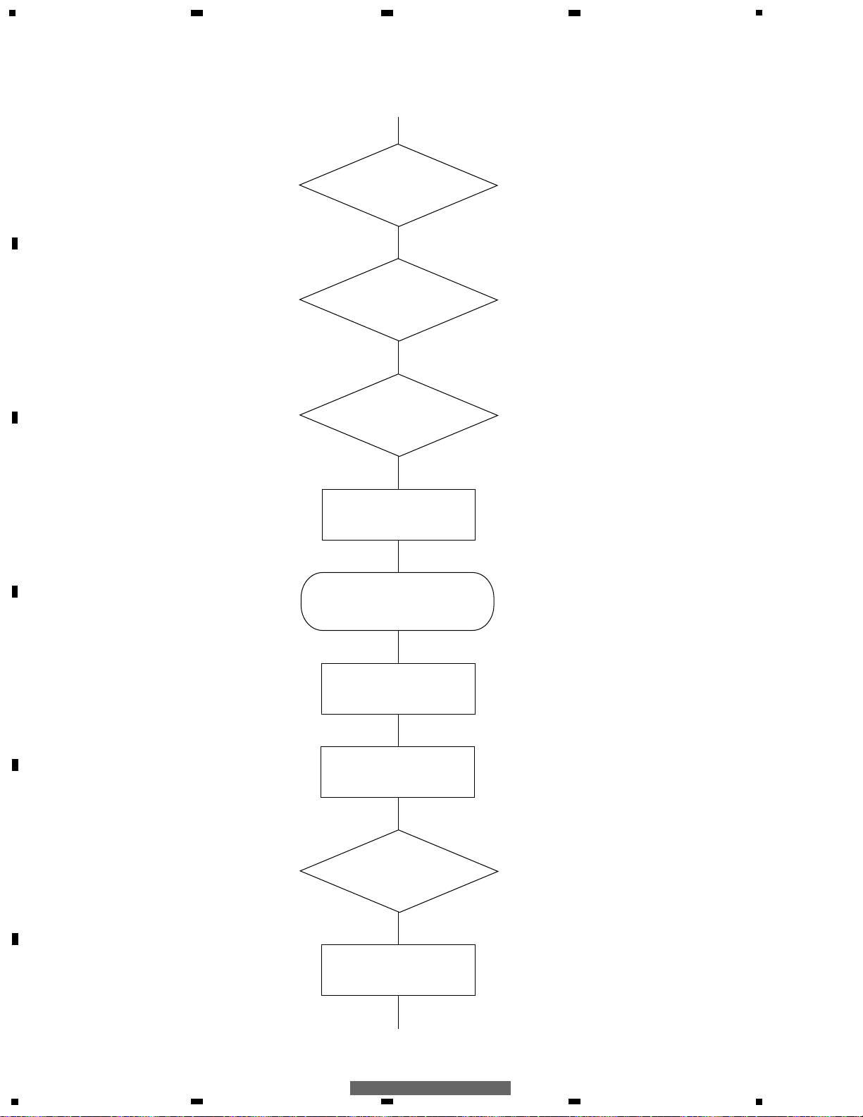
POWER ON
VDD=5V
13 pin
bsens
16 pin
asens
17 pin
IPPW←H
19 pin
Starts communication
with AVC-LAN
swvdd←L
74 pin
Source keys
operative
Source ON
SYSPW←H
63 pin
Completes power-on operation.
(After that, proceed to each source operation.)
bsens=L
asens=L
YES
YES
7.3 OPERATIONAL FLOW CHART
Page 47

47
5
6
7
8
F
E
D
C
B
A
5
6
7
8
KEH-M8027ZT/XN/ES
7.4 CLEANING
Before shipping out the product, be sure to clean the following portions by using the prescribed cleaning tools:
Portions to be cleaned Cleaning tools
Cassette heads
Pinch rollers Cleaning paper : GED-008
Capstans
Page 48

Listening to the Radio
Power On/Off, Volume
Power On/Off
Push the power button to turn the unit on or
off.
Volume Control
T o increase the volume, turn knob to the right.
To decrease the volume, turn it to the left.
Lights up when an FM stereo broadcast is being received
Lights up during SCAN or Preset Scan
Band Preset number Frequency
AM/FM1Æ2
If you press the AM button, power to the ra-
dio switches on and an AM broadcast is re-
ceived.
If you press the FM1·2 button, power to the
radio switches on.
Each time you press the button, the setting
changes as below.
FM1 FM2
1
2
6
3
547
1
2
Automatic Tuning
Broadcast stations above a certain signal
strength can be tuned into automatically.
To cancel, press the button again.
Press the button down either on the “ ” side
or the “ ” side. The automatic tuning will start,
and the radio will find and tune into the sta-
tion.
Manual Tuning
This is useful to tune into a station with a weak
signal that cannot be found with the automatic
tuning.
Turn the knob clockwise or counterclockwise
until you find the frequency you want.
Preset Memory
This function is used to memorize radio sta-
tions. To memorize a station:
Choose one button and press it down for
about 1.7 seconds until you hear a beep.
To select a memorized station:
Having memorized a station, you can press
the same button again and within 1.7 sec-
onds the radio will tune into that memorized
station.
AM Tuning Step
The tuning step employed in the radio’s AM
band can be switched between 9 kHz and 10
kHz per step. Reset the tuning step from 9
kHz (the factory preset step) to 10 kHz when
you want to receive a 10 kHz step broadcast
station (530 – 1,710 kHz) in Vietnam.
Initial setting: 9 kHz step (531 – 1,602 kHz)
New setting: 10 kHz step (530 – 1,710 kHz)
1. Push the power button to turn the unit
off.
2. Simultaneously press buttons 2 and 5 of
more than 1.7 seconds. The current AM
tuning step is indicated in the display.
3. Press the “
” or “ ” side of to select
the tuning step.
4. Simultaneously press buttons 2 and 5 of
.
A beep sounds to inform you that the tun-
ing step has changed and preset memory
will be cleared.
Preset Scan
The radio will automatically tune in to all of
your preset stations which are of a certain
signal strength one by one for about 10 sec-
onds each.
Keep the button pressed for more than 1.7
seconds, until you hear a beep. T o cancel the
preset scan, press the button again.
• If you choose Preset Scan on the FM
waveband, it will be automatically carried
out on both FM1 and FM2.
• Preset Scan is for reception of strong broad-
cast station transmissions only. You can-
not use it for reception of weak broadcast
station transmissions.
Scan
The radio will automatically tune in to stations
which are of a certain signal strength in turn
for about 10 seconds each.
Press the button quickly (for less than 1.7
seconds). To cancel the scan, press the but-
ton again.
Mode
This selects the volume and tone adjustment
modes. Press the knob to change the mode.
After selecting the mode, adjust using this
knob.
BAS (Bass)
TRE (Treble)
FAD (Fader)
BAL (Balance)
Adjustment
Carry out adjustment of the mode selected
with this knob. Adjust by turning the knob
clockwise or counterclockwise.
3
4
5
6
7
1
5
5
3
DOLBY B NR
48
1
234
12
34
F
E
D
C
B
A
KEH-M8027ZT/XN/ES
8. OPERATIONS AND SPECIFICATIONS
8.1 OPERATIONS
Page 49

49
5
6
7
8
F
E
D
C
B
A
5
6
7
8
KEH-M8027ZT/XN/ES
Listening to tape
Tape Slot
If you insert a cassette tape into the tape slot,
tape playback begins.
• This product is compatible with metal tapes.
Tape Eject
If you press the tape eject button, the cas-
sette tape is ejected.
A cassette can be ejected even if the ve-
hicle engine switch is turned to the OFF
position.
Tape
Pressing the tape button switches on the
power to the tape player, and playback be-
gins. When there is no cassette tape inserted
in the machine, the power is not switched on.
Dolby B NR indicator (Dolby NR B-Type)
Tape Direction
Repeat play indicator
2
13
7
68
5
4
1
2
3
Dolby B NR
When playing a cassette recorded in Dolby
NR mode, press the Dolby B NR button.
“” will light.
To cancel the Dolby B NR setting, press the
same button once again.
• Manufactured under license from Dolby
Laboratories. “Dolby” and the double-D
symbol are trademarks of Dolby Laborato-
ries.
Tape Direction
Press the tape direction button.
Fast-Forwarding and Rewinding
Press the button to fast forward or
to rewind the tape. To stop fast forward or
rewind, press the same button again or press
the TAPE button.
Start of a Track
You can skip forward or go back to the start
of a track you like to choose within previous
9 tracks and next 9 tracks of the track being
played.
Press the start of track button as many as
you like to skip (3 times if you like to skip to
the third track).
The track being played is counted when you
rewind.
• Press the “” side of the start of track but-
ton to skip forward.
• Press the “” side to go back.
The cancel this function, press the tape but-
ton.
The start of track function may not work
properly in the following cases:
¥ If there is a blank section of less than 3
seconds between tracks
¥ If there is noise between tracks
Repeat
Press the repeat button.
“RPT” will light.
To cancel the repeat function, press the re-
peat button once again.
The repeat function may not work prop-
erly in the following cases:
¥ If there is a blank section of less than 3
seconds between tracks
¥ If there is noise between tracks
4
5
6
7
8
DOLBY B NR
Page 50

1
234
12
34
F
E
D
C
B
A
KEH-M8027ZT/XN/ES
Listening to a CD
Connect a CD CHANGER or Single CD PLAYER,
and you can operate it with this unit.
The “*” mark indicates functions you can use only
when a CD CHANGER is connected.
CD
Pressing this button starts CD playback.
Disc*
Press the disc change button.
Track
Press the track button ( or ) to select a
desired track number.
• Press to move ahead.
• Press to move back.
Fast Forward/Reverse
Press the fast forward/reverse button (
or ) for one second or longer.
When you take your finger off the fast for-
ward/reverse button, playback will start at that
position.
Scan indicator
Random play indicator
Disc mode indicator
Repeat play indicator
Disc number
Track number
Play time
1
53 4
67
2
3
4
1
2
Scan
To play the first 10 seconds of each track
on the CD being played
1. Press the scan button.
“SCAN” will light.
2. When you reach the track you want to hear,
press the scan button once again.
Playback will then continue from that track.
To play the first 10 seconds of the first
track of each CD in the magazine*
1. Press the scan button until you hear a
beep.
“
SCAN” will light.
2. When you reach the disc you want to hear,
press the scan button once again.
Playback will then continue from that disc.
Repeat
Repeating the track being played
Press the repeat button.
“RPT” will light.
Pressing the repeat button again will cancel
the repeat function.
Repeating the disc being played*
Press the repeat button until you hear a beep.
“
RPT” will light.
Pressing the repeat button again will cancel
the disc repeat function.
Random
To play tracks on the disc being played in
random order
Press the random play button.
“RAND” will light.
Pressing the random button again will cancel
the random play function.
To play tracks on all discs in the maga-
zine in random order*
Press the random play button until you hear
a beep.
“
RAND” will light.
Pressing the random button again will cancel
the disc random play function.
¥ Since tracks are played in random or-
der, the same track may be played twice
in succession.
5
6
7
Error Indications
If the CD autochanger does not work, the CD stops suddenly during playback, or a similar problem occurs, an
error indication will appear on the display. The cause of the trouble will be indicated by an error number, and
you should check the corresponding item shown in the table below.
Display Description
LOAd Appears while the CD changer is searching for a disc.
Err1
This appears when the disc is dirty or upside-down.
Check the disc.
Err2
This appears when no disc is set in the CD changer.
Set a disc in the CD changer.
Err3
This appears when the CD player does not work due to some trouble.
Take the CD out of the CD player.
Err4
This appears when there is an excess current flow due to some trouble.
Take the CD out of the CD player.
WAIT
This appears when the CD player does not work because its temperature is high.
Wait a short while until the temperature becomes low.
* Some of the indications may not appear depending on the CD player built into this equipment.
DOLBY B NR
 Loading...