

Page 1
PIONEER CORPORATION 4-1, Meguro 1-Chome, Meguro-ku, Tokyo 153-8654, Japan
PIONEER ELECTRONICS (USA) INC. P.O.Box 1760, Long Beach, CA 90801-1760 U.S.A.
PIONEER EUROPE NV Haven 1087 Keetberglaan 1, 9120 Melsele, Belgium
PIONEER ELECTRONICS ASIACENTRE PTE.LTD. 253 Alexandra Road, #04-01, Singapore 159936
C PIONEER CORPORATION 2004
K-ZZB. APR. 2004 Printed in Japan
ORDER NO.
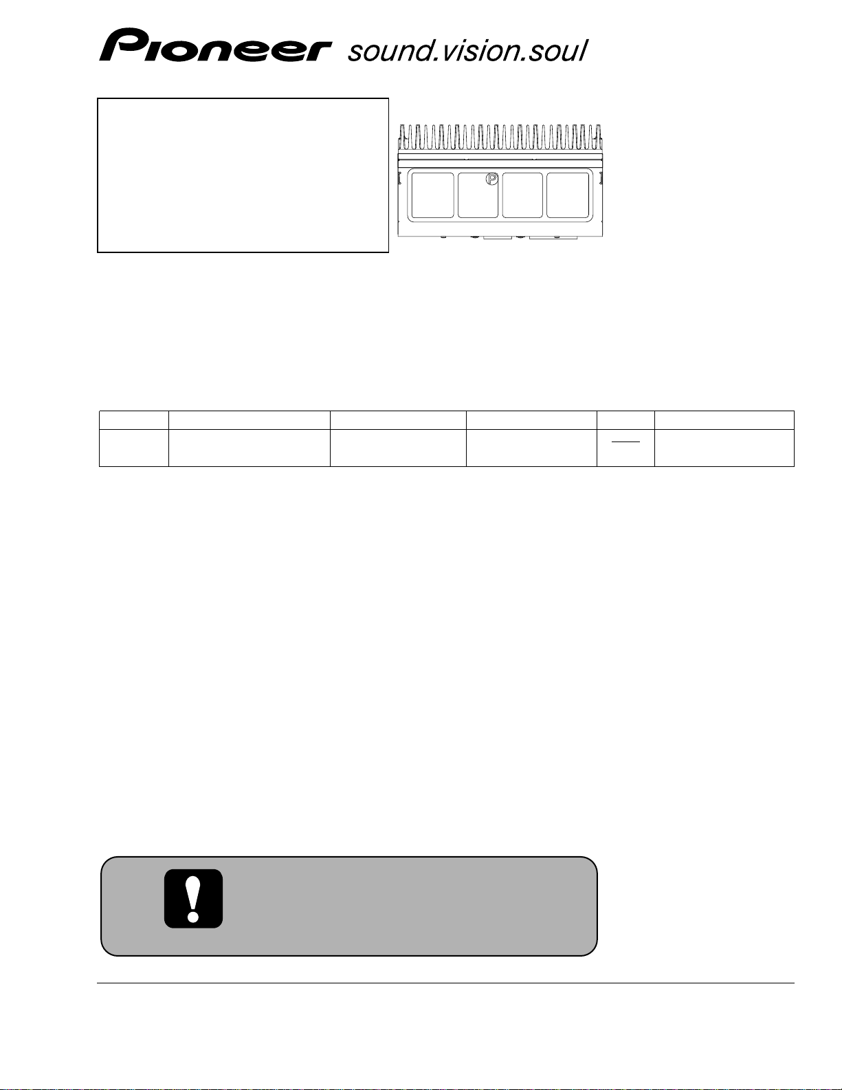
CRT3180
POWER AMPLIFIER
GM-8437
ZTWL
TOYOTA
VEHICLE DESTINATION PRODUCED AFTER TOYOTA PART No. ID No. PIONEER MODEL No.
CROWN Singapore, Hong Kong, December 2004 86280-30470 GM-8473ZT/WL
Thailand, Indonesia
GM-8437ZT/WL
For details, refer to "Important symbols for good services".
Page 2
2
1
234
12
34
F
E
D
C
B
A
GM-8437ZT/WL
[ Important symbols for good services ]
In this manual, the symbols shown-below indicate that adjustments, settings or cleaning should be made securely.
When you find the procedures bearing any of the symbols, be sure to fulfill them:
2. Adjustments
To keep the original performances of the product, optimum adjustments or specification confirmation is indispensable.
In accordance with the procedures or instructions described in this manual, adjustments should be performed.
3. Cleaning
For optical pickups, tape-deck heads, lenses and mirrors used in projection monitors, and other parts requiring cleaning,
proper cleaning should be performed to restore their performances.
5. Lubricants, glues, and replacement parts
Appropriately applying grease or glue can maintain the product performances. But improper lubrication or applying
glue may lead to failures or troubles in the product. By following the instructions in this manual, be sure to apply the
prescribed grease or glue to proper portions by the appropriate amount.For replacement parts or tools, the prescribed
ones should be used.
4. Shipping mode and shipping screws
To protect the product from damages or failures that may be caused during transit, the shipping mode should be set or
the shipping screws should be installed before shipping out in accordance with this manual, if necessary.
1. Product safety
You should conform to the regulations governing the product (safety, radio and noise, and other regulations), and
should keep the safety during servicing by following the safety instructions described in this manual.
SAFETY INFORMATION
This service manual is intended for qualified service technicians; it is not meant for the casual do-it-yourselfer.
Qualified technicians have the necessary test equipment and tools, and have been trained to properly and safely repair
complex products such as those covered by this manual.
Improperly performed repairs can adversely affect the safety and reliability of the product and may void the warranty.
If you are not qualified to perform the repair of this product properly and safely, you should not risk trying to do so
and refer the repair to a qualified service technician.
NOTE:
- When diagnosing a product, take care of its heated portion.
Power IC (IC802,803)
Power Supply IC (IC901,902)
DSP IC (IC301,311)
Heat Sink
IC Holder
- Service Precaution
You should conform to the regulations governing the product (safety, radio and noise, and other regulations),
and should keep the safety during servicing by following the safety instructions described in this manual.
Page 3

3
5
6
7
8
F
E
D
C
B
A
5
6
7
8
GM-8437ZT/WL
CONTENTS
SAFETY INFORMATION............................................2
1. SPECIFICATIONS.......................................................3
2. EXPLODED VIEWS AND PARTS LIST ......................4
2.1 EXTERIOR............................................................4
3. BLOCK DIAGRAM AND SCHEMATIC DIAGRAM ....6
3.1 BLOCK DIAGRAM ...............................................6
3.2 SCHEMATIC DIAGRAM(GUIDE PAGE) ..............8
4. PCB CONNECTION DIAGRAM................................14
4.1 DSP UNIT...........................................................14
4.2 AMP ASSY.........................................................18
4.3 ASL UNIT...........................................................22
5. ELECTRICAL PARTS LIST........................................23
6. ADJUSTMENT.........................................................28
7. GENERAL INFORMATION.......................................30
7.1 DIAGNOSIS .......................................................30
7.1.1 DISASSEMBLY.........................................30
7.1.2 CONNECTOR FUNCTION DESCRIPTION
......32
7.1.3
THE METHOD OF DISTINGUISHING DEFECTIVE
DSP IC(IC301 OR IC311) DURING DSP ERROR .....
33
7.2 IC ........................................................................35
7.3 EXPLANATION...................................................40
7.3.1 SYSTEM BLOCK DIAGRAM.....................40
7.3.2 OPERATIONAL FLOW CHART .................41
8. OPERATIONS...........................................................41
1. SPECIFICATIONS
Power source . . . . . . . . . . . . .13.2±0.1V(10.5-16.0V)
Grounding . . . . . . . . . . . . . . . .Negative type
Backup current . . . . . . . . . . . .0.3mA or less
Dimensions . . . . . . . . . . . . . . .235mm(W)x51mm(H)x128mm(D)
Weight . . . . . . . . . . . . . . . . . . .1348g
Maximum output power . . . .22W or more(Front)
11W or more(Center)
22W or more(Rear)
35W or more(Woofer)
Page 4
4
1
234
12
34
F
E
D
C
B
A
GM-8437ZT/WL
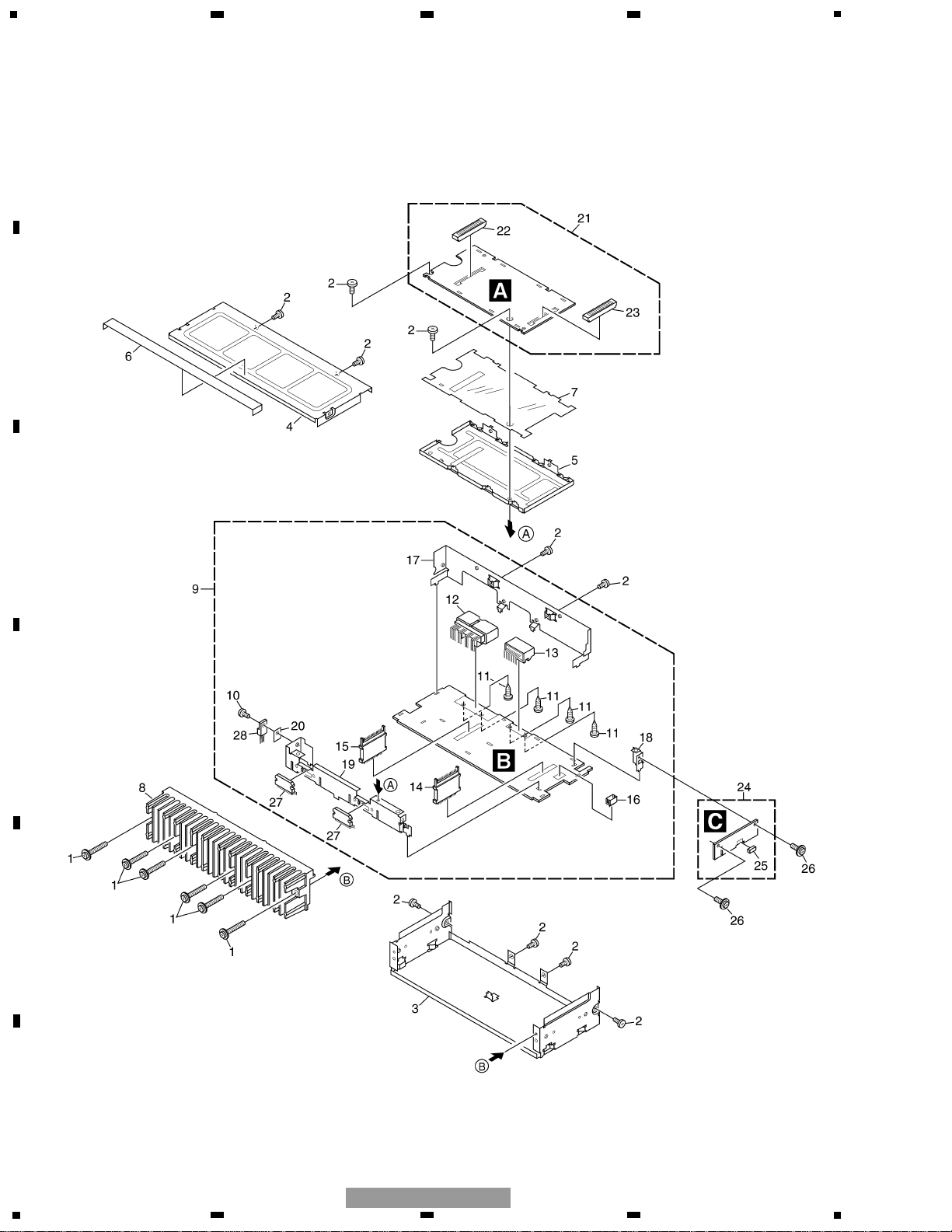
2. EXPLODED VIEWS AND PARTS LIST
2.1 EXTERIOR
Page 5

5
5
6
7
8
F
E
D
C
B
A
5
6
7
8
GM-8437ZT/WL
1 Screw AMZ30P220FTC
2 Screw BSZ26P060FTC
3 Chassis CNA2493
4 Case CNB2743
5 Shield Case CND1276
6 Seal CNM6686
7 Insulator CNM7999
8 Heat Sink CNR1641
9 Amp Assy CWM8256
10 Screw BSZ26P080FTC
11 Screw(M3x6) CBA1393
12 Connector(CN901) CKM1363
13 Connector(CN902) CKM1364
14 Plug(CN905) CKS4569
15 Plug(CN906) CKS4569
16 Connector(CN404) CKS4639
17 Bracket CNC9890
18 Holder CNC9893
19 Holder CND1275
20 Sheet CNM7015
21 DSP Unit CWM8259
22 Socket(CN101) CKS4616
23 Socket(CN102) CKS4616
24 ASL Unit CWM8925
25 Connector(CN403) CKS4605
26 Screw IMS26P060FTC
27 IC(IC802,803) PAL006A
28 IC(IC902) BA178M05T
NOTE:
- Parts marked by “*” are generally unavailable because they are not in our Master Spare Parts List.
- Screws adjacent to ∇ mark on the product are used for disassembly.
- For the applying amount of lubricants or glue, follow the instructions in this manual.
( In the case of no amount instructions, apply as you think it appropriate.)
- EXTERIOR SECTION PARTS LIST
Mark No. Description Part No.
Page 6
6
1
234
12
34
F
E
D
C
B
A
GM-8437ZT/WL
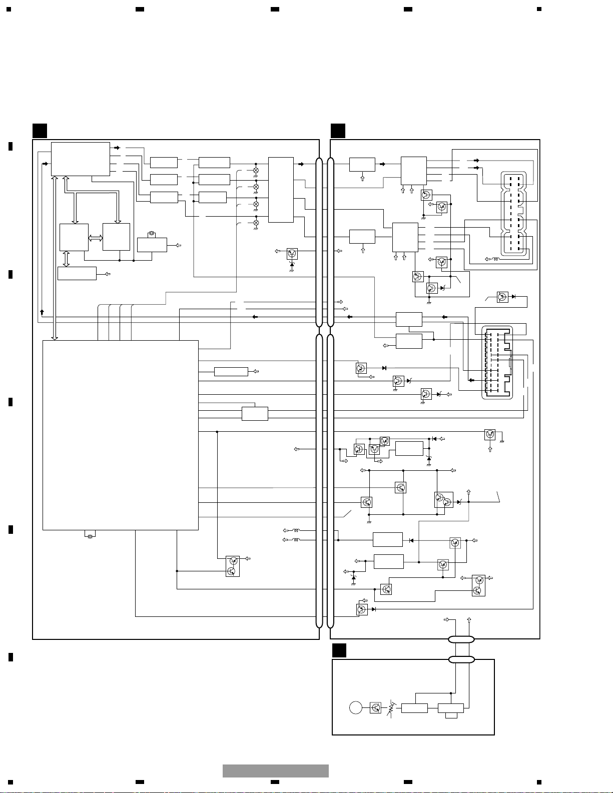
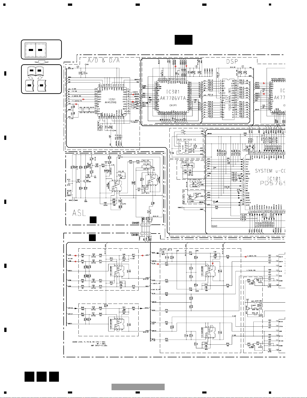
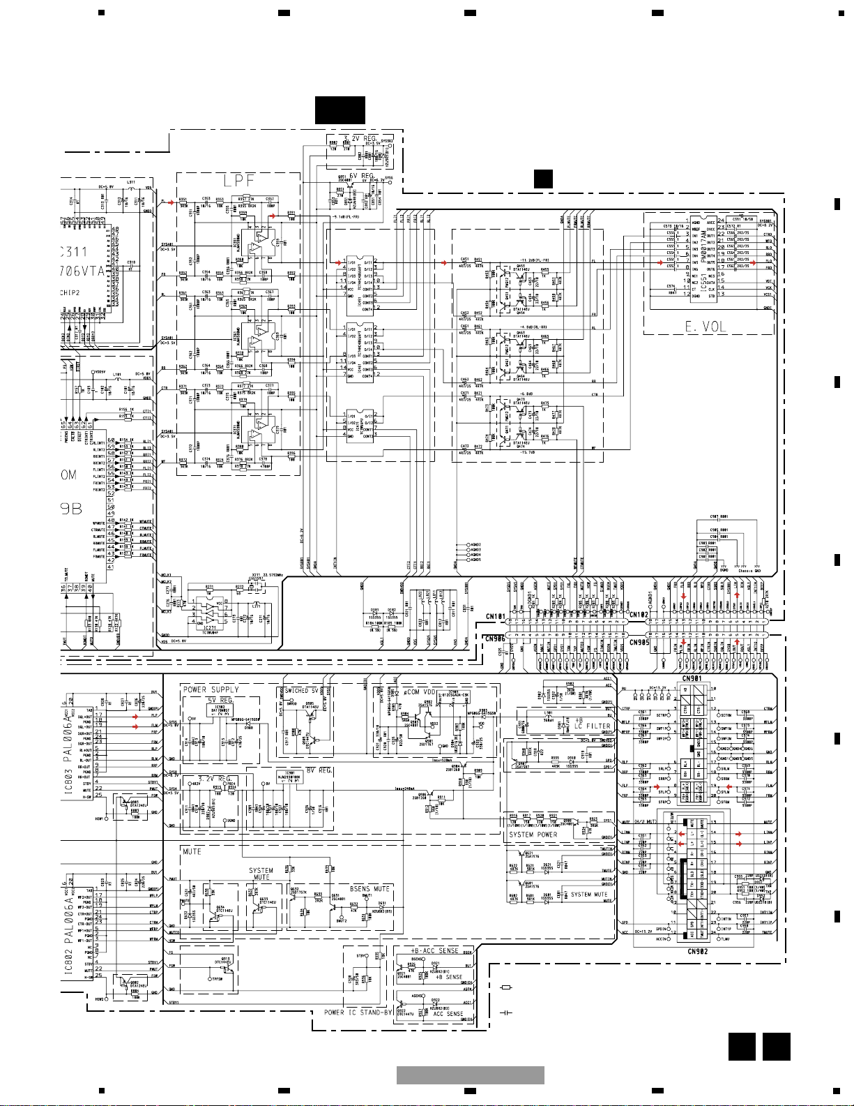
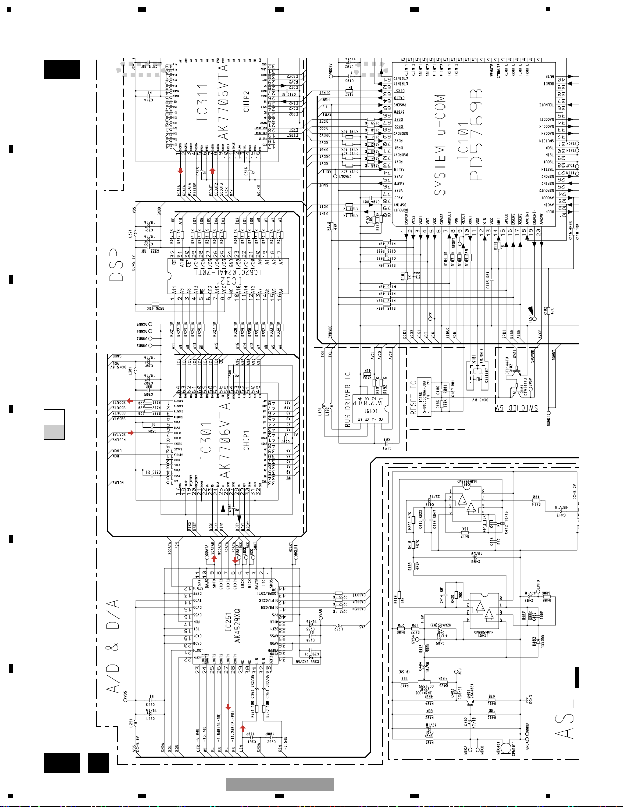
3. BLOCK DIAGRAM AND SCHEMATIC DIAGRAM
3.1 BLOCK DIAGRAM
DSP UNIT
A
27
LOUT1
A/D & D/A
32
RIN
IC251
31
LIN
AK4529XQ
XTI
39
DATA,BCK,LRCK
IC62C1024AL-70TI
DACCSN,DACCLK,DACDTI,SMUT,PDN
IC301
AK7706VTA
MCLK2
A0-16
IO0-7
we,oe
IC321
DSP
16
SYSTEM CONTROLLER
LOUT2
LOUT3
ROUT3
MCLK1
8
44
FLMUTE
PD5769B
25
23
(CTR)
24
(WF)
IC311
AK7706VTA
MCLK3
16
VDD5
48
46
RLMUTE
IC101
(FL)
(RL)
47
WFMUTE
TC7WU04F
CTRMUTE
FRONT LPF
2
NJM4580MD
REAR LPF
2
NJM4580MD
WOOFER LPF
2
6
NJM4580MD
X271
1
IC271
2
7
IC351
IC361
IC371
EXTERNAL INPUT
CHANGE
1
1
(FL)
4
TC74HC4066AFT
1
1
(RL)
4
TC74HC4066AFT
1
1
(CTR)
IC471
7
5
TC7W66FU
(WF)
8
VDD5
74
21
BEEP
ASLIN
31
SMUTEIN
9
reset
17
asens
16
bsens
20
AVCP W
22
AVCI N
23
AVCOUT
65
PWSENS
IC451
IC461
1
S-80835CNUA-B8U
INPUT CHANGE
2
2
2
(BEEP)
(ASL1)
RESET
IC186
MUTE FOR
EXTERNAL
(FL)
(RL)
(CTR)
(WF)
2
BUS DRIVER
2
IC191
HA12187FP
1
7
5
3
4
VCC
VDD5
8
ELECTRONIC
VOLUME
IN5
IN3
IC551
PM0017AM
IN1
IN2
6V REG.
6
5
OUT5
OUT3
OUT1
OUT2
Q851
VDD
CN102
18
FLO
20
RLO
22
CTRO
21
WFO
SYS801
INT1IN
BEEP
ASL1
LIN
RIN
CN101
MUTI
ASEN
BSEN
TXH TXP
TXL TXM
VDD5
13
11
9
10
6
2
1
3
5
4
12
14
3
811
910
FS FS
514
1
40
MUTE
64
calib
36
TELMUTE
XOUT
10 12
X101
XIN
SPEED
15
SYSPW
66
SWITCHED 5V
Q101
VDD5
Q102
MUTO
7
HSW
6
TMUT
2
SYSA5
VA5
VD5
SYS1
17 2
10
11 8
B
CN905
13
11
CTRIN
9
WFIN
10
6
2
1
3
LOUT
5
4
7
5
16
18
MUTEO
12
13
17
TMUTEIN
118
9
C
FLIN
RLIN
SYS8
INT1O
BEEP
ROUT
CN906
MUTIN
ASEN
BSEN
VDD5
HSW
SYS5SYSD5
SYS8
SYS4
SYS1
Q907
SPD1SPD1
AMP ASSY
GAIN ADJ
13
IC701
NJM4580MD
2
BEEP
GAIN ADJ
75
IC751
NJM4580MD
6
SYS4
ASL1
SYSTEM MUTE
VDD5
PMUT
Q601
Q901
BALANCE→UNBALANCE
SYS8
SWDVDD
Q902
Q903
ACC
SYSTEM
Q633
Q634
B
MUTE
5V REGULATOR
IC902
1
BA178M05T
8V REGULATOR
IC901
1
NJM2930F08K
Q908
SWDVDD
SPEED PULSE SENSE
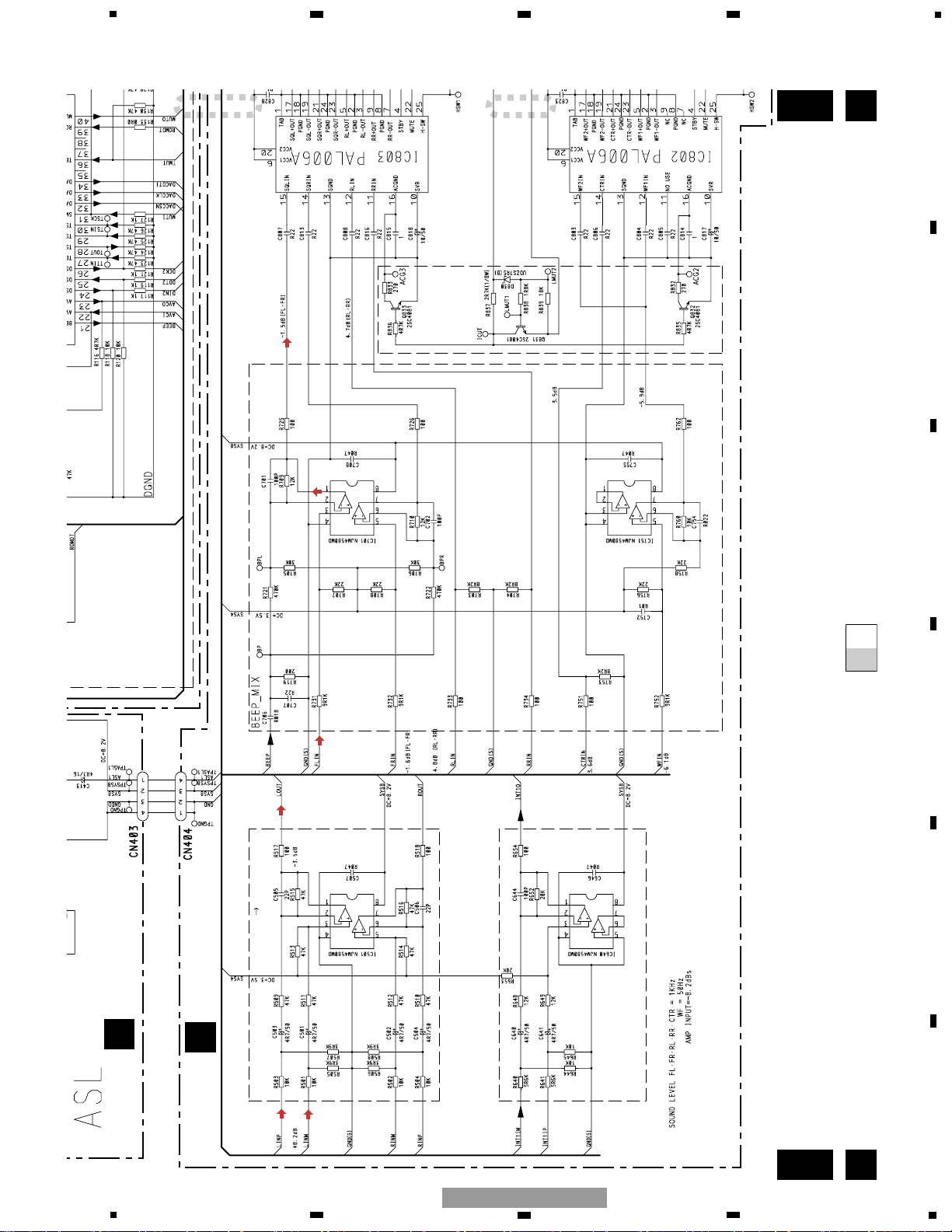
ASL UNIT
POWER AMP
15
IC803
PAL006A
12
4
22
10
STBY1
PMUT
POWER AMP
IC802
PAL006A
10
4
22
PMUT
STBY1
1
IC501
7
NJM4580MD
5
1
IC640
8
NJM4580MD
VOICE INTERRUPTION
INPUT DIFFERENTIAL
ACC SENSE
Q922
IC903
3
S-812C56AUA-C3K
µCOM VDD
Q832
23
21
3
5
FSW
2
6
3
Q921
2
14
12
OPERATIONAL AMPLIFIER
MUTE
Q632
3
3
SYSTEM POWER
SYSPW1
17
19
3
5
Q833
Q803
FSW
(CTR-)
(CTR+)
(WF-)
(WF+)
Q802
Q831
LINP
RINP
BACK UP SENSE
BU1
BSENSE
MUTE
Q906
SYS8
CN404
CN403
(RL-)
(RL+)
BU1
Q631
(FLP)
(FLM)
A
(ACC)
SYS8
STBY1
Q904
SWITCHED 5V
SWDVDD
ASL1
34
21
INT1+
MUTE
Q909
TMUT
R+
L+
Q905
BU1
B
Q913
BU1
CONNECTOR
FL-
RL-
WF-
CTR-
TEL MUTE
Q621
CN902
INPUT
CONNECTOR
OUTPUT OFFSET
INDICATION
FSW
A
VDD5
OUTPUT
CN901
ACC
SPD
TX+
TX-
FL+
RL+
WF+
CTR+
(SPD)
(TX+)
(TX-)
ASL
Q401
VR401
5
NJM4580MD
IC401
8
8
3
77
IC402
NJM4580MD
15
MIC401
MIC
Page 7

7
5
6
7
8
F
E
D
C
B
A
5
6
7
8
GM-8437ZT/WL
Page 8
8
1
234
12
34
F
E
D
C
B
A
GM-8437ZT/WL
A-aA-a A-b A-b
A-aA-a
A-b A-b
A-b A-b
A-a A-a
Large size
SCH diagram
Guide page
Detailed page
Note: When ordering service parts, be sure to refer to " EXPLODED VIEWS AND PARTS LIST" or
"ELECTRICAL PARTS LIST".
A-a
A B C
SIGNAL INPUT
OFF CIRCUIT TO
SUDDEN DECREASE
VOLTAGE
GAIN ADJUSTMENT
BALANCE UNBALANCE
AUDIO INPUT DIFFERENTIAL
OPERATIONAL AMPLIFIER
VOICE INTERRUPTION
INPUT DIFFERENTIAL
OPERATIONAL AMPLIFIER
(BALANCE)
C
ASL UNIT
B
AMP ASSY
CD:-3.5dBs
CD:+8.2dBs
(1kHz, 0dB)
CD:+1.7dBs
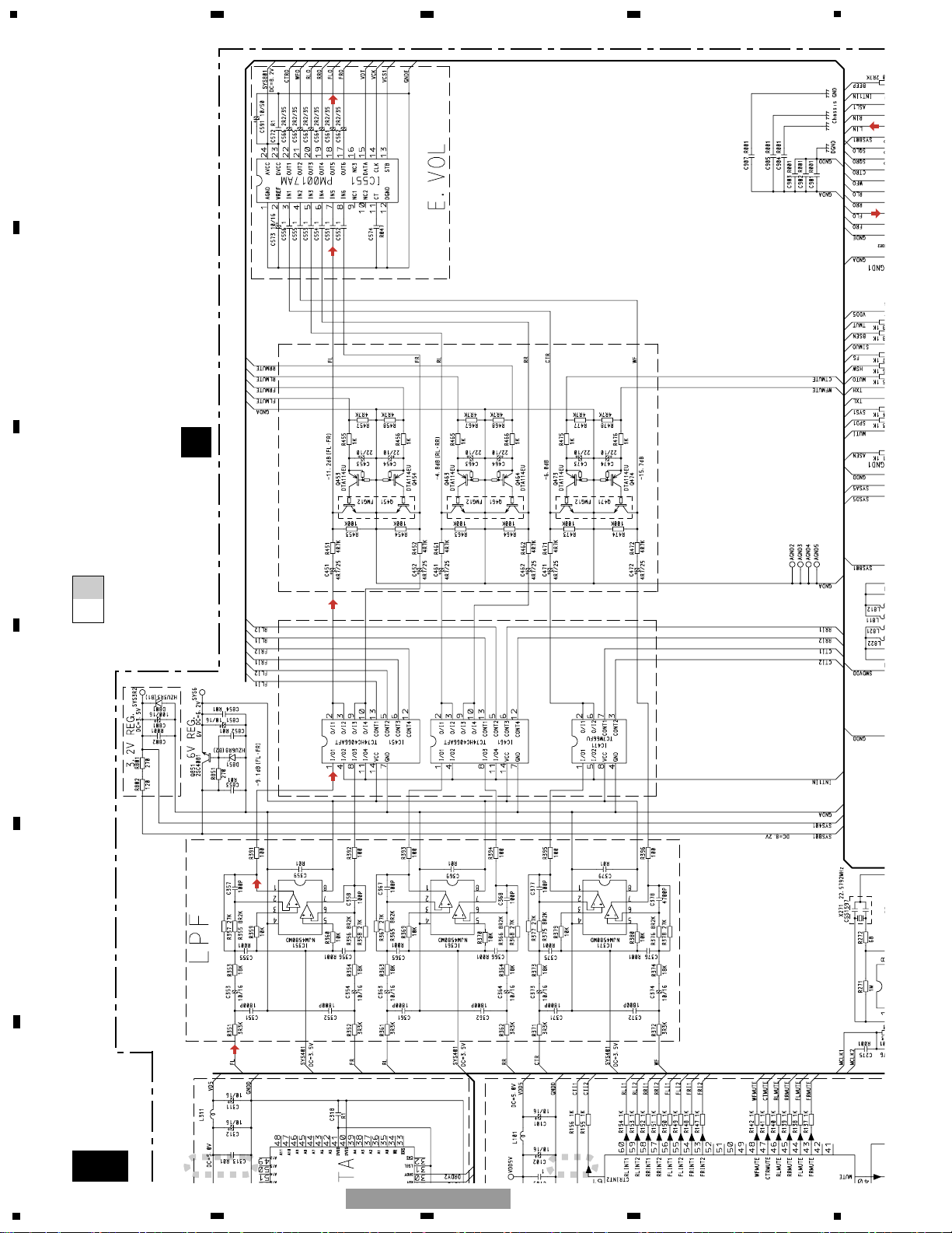
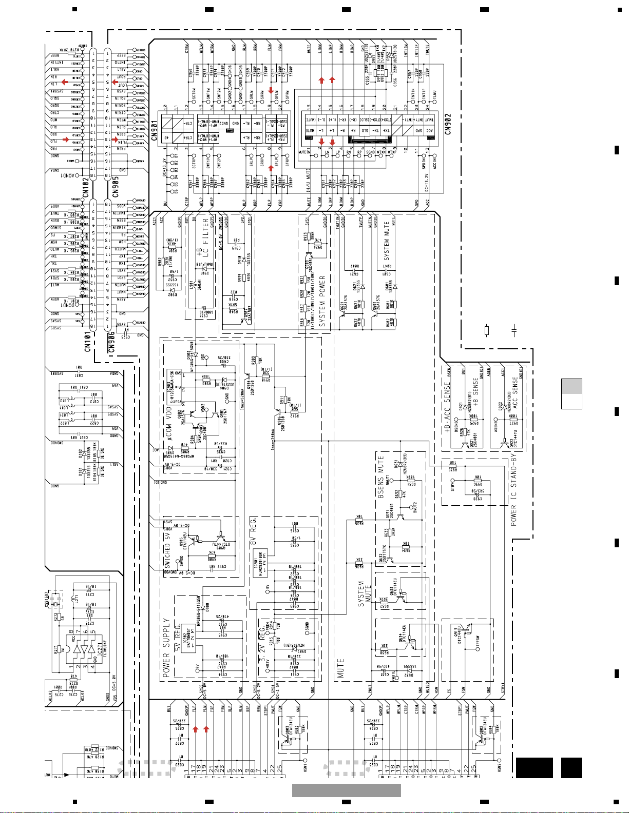
3.2 SCHEMATIC DIAGRAM (GUIDE PAGE)
Page 9
9
5
6
7
8
F
E
D
C
B
A
5
6
7
8
GM-8437ZT/WL
A-b
A B
EXTERNAL INPUT
CHANGE
MUTE FOR
EXTERNAL INPUT CHANGE
SPEED PULSE SENSE
OUTPUT OFFSET
INDICATION
OUTPUT OFFSET
INDICATION MUTE
OUTPUT OFFSET
INDICATION
OUTPUT OFFSET
INDICATION
A
DSP UNIT
Decimal points for resistor
and capacitor fixed values
are expressed as :
2.2 2R2
0.022 R022
←
←
Symbol indicates a resistor.
No differentiation is made between chip resistors and
discrete resistors.
NOTE :
Symbol indicates a capacitor.
No differentiation is made between chip capacitors and
discrete capacitors.
MAY DAY MUTE
(HELP NET MUTE)
CD:+27.7dBs
CD:-5.87dBs
CD:+2.0dBs
Page 10
10
1
234
12
34
F
E
D
C
B
A
GM-8437ZT/WL
A-a
A-b
A-a
A-a
A-b
C
1
2
C
CD:-3.5dBs
Page 11
11
5
6
7
8
F
E
D
C
B
A
5
6
7
8
GM-8437ZT/WL
A-a
A-b
A-a
A-a
B
A-a
B
3
4
SIGNAL INPUT
OFF CIRCUIT TO
SUDDEN DECREASE
VOLTAGE
GAIN ADJUSTMENT
BALANCE UNBALANCE
AUDIO INPUT DIFFERENTIAL
OPERATIONAL AMPLIFIER
VOICE INTERRUPTION
INPUT DIFFERENTIAL
OPERATIONAL AMPLIFIER
(BALANCE)
C
ASL UNIT
B
AMP ASSY
CD:+8.2dBs
(1kHz, 0dB)
CD:+1.7dBs
Page 12
12
1
234
12
34
F
E
D
C
B
A
GM-8437ZT/WL
A-a
A-b
A-b
1
2
EXTERNAL INPUT
CHANGE
MUTE FOR
EXTERNAL INPUT CHANGE
A
DSP UNIT
CD:-5.87dBs
CD:+2.0dBs
Page 13
13
5
6
7
8
F
E
D
C
B
A
5
6
7
8
GM-8437ZT/WL
A-a
A-b
A-a
B
3
4
SPEED PULSE SENSE
OUTPUT OFFSET
INDICATION
OUTPUT OFFSET
INDICATION MUTE
OUTPUT OFFSET
INDICATION
OUTPUT OFFSET
INDICATION
MAY DAY MUTE
(HELP NET MUTE)
Decimal points for resistor
and capacitor fixed values
are expressed as :
2.2 2R2
0.022 R022
←
←
Symbol indicates a resistor.
No differentiation is made between chip resistors and
discrete resistors.
NOTE :
Symbol indicates a capacitor.
No differentiation is made between chip capacitors and
discrete capacitors.
CD:+27.7dBs
Page 14

14
1
234
12
34
F
E
D
C
B
A
GM-8437ZT/WL
4. PCB CONNECTION DIAGRAM
4.1 DSP UNIT
Capacitor
Connector
P.C.Board
Chip Part
A
A
DSP UNIT
SIDE B
SIDE A
NOTE FOR PCB DIAGRAMS
1.The parts mounted on this PCB
include all necessary parts for
several destination.
For further information for
respective destinations, be sure
to check with the schematic dia gram.
2.Viewpoint of PCB diagrams
B
CN906
Page 15

15
5
6
7
8
F
E
D
C
B
A
5
6
7
8
GM-8437ZT/WL
A
SIDE A
B
CN905
Page 16

16
1
234
12
34
F
E
D
C
B
A
GM-8437ZT/WL
A
A
DSP UNIT
Page 17

17
5
6
7
8
F
E
D
C
B
A
5
6
7
8
GM-8437ZT/WL
A
SIDE B
Page 18

18
1
234
12
34
F
E
D
C
B
A
GM-8437ZT/WL
4.2 AMP ASSY
B
B
AMP ASSY
A
CN101
Page 19

19
5
6
7
8
F
E
D
C
B
A
5
6
7
8
GM-8437ZT/WL
B
SIDE A
A
CN102
C
CN403
Page 20

20
1
234
12
34
F
E
D
C
B
A
GM-8437ZT/WL
B
B
AMP ASSY
Page 21

21
5
6
7
8
F
E
D
C
B
A
5
6
7
8
GM-8437ZT/WL
B
SIDE B
Page 22

22
1
234
12
34
F
E
D
C
B
A
GM-8437ZT/WL
4.3 ASL UNIT
C
C
ASL UNIT
C
ASL UNIT
SIDE A
SIDE B
B
CN404
Page 23

23
5
6
7
8
F
E
D
C
B
A
5
6
7
8
GM-8437ZT/WL
Unit Number : CWM8259
Unit Name : DSP Unit
MISCELLANEOUS
IC 101 IC PD5769B
IC 186 IC S-80835CNUA-B8U
IC 191 IC HA12187FP
IC 251 IC AK4529XQ
IC 271 IC TC7WU04F
IC 301 IC AK7706VTA
IC 311 IC AK7706VTA
IC 321 IC IC62C1024AL-70TI
IC 351 IC NJM4580MD
IC 361 IC NJM4580MD
IC 371 IC NJM4580MD
IC 451 IC TC74HC4066AFT
IC 461 IC TC74HC4066AFT
IC 471 IC TC7W66FU
IC 551 IC PM0017AM
Q 101 Transistor DTA144EU
Q 102 Transistor DTC144TU
Q 451 Transistor FMG12
Q 453 Transistor DTA114EU
Q 454 Transistor DTA114EU
Q 461 Transistor FMG12
Q 463 Transistor DTA114EU
Q 464 Transistor DTA114EU
Q 471 Transistor FMG12
Q 473 Transistor DTA114EU
Q 474 Transistor DTA114EU
Q 851 Transistor 2SC4081
D 181 Diode 1SS355
D 182 Diode 1SS355
D 801 Diode HZU3R3(B1)
D 851 Diode HZU6R8(B2)
L 101 Inductor LCTC1R0K2125
L 191 Inductor CTF1305
L 192 Inductor CTF1305
L 251 Inductor LCTC1R0K2125
L 252 Inductor LCTC1R0K2125
L 271 Inductor LCTC1R0K2125
L 301 Inductor LCTCR82K2125
L 311 Inductor LCTCR82K2125
L 321 Inductor LCTCR82K2125
L 811 Inductor LCTC1R0K3216
L 812 Inductor LCTC1R0K3216
L 821 Inductor LCTA2R2J2520
L 822 Inductor LCTA2R2J2520
X 101 Radiator 10.0MHz CSS1607
X 271 Radiator 22.5792MHz CSS1597
RESISTORS
R 101 RS1/16S102J
R 102 RS1/16S473J
R 103 RS1/16S103J
R 104 RS1/16S102J
R 105 RS1/16S473J
R 107 RS1/16S102J
R 108 RS1/16S102J
R 109 RS1/16S681J
R 110 RS1/16S102J
R 111 RS1/16S473J
R 112 RS1/16S104J
R 113 RS1/16S104J
R 116 RS1/16S472J
R 117 RS1/16S102J
R 118 RS1/16S103J
R 119 RS1/16S102J
R 120 RS1/16S103J
R 121 RS1/16S102J
R 122 RS1/16S472J
R 123 RS1/16S473J
R 124 RS1/16S473J
R 125 RS1/16S473J
R 126 RS1/16S473J
R 127 RS1/16S102J
R 128 RS1/16S473J
R 130 RS1/16S473J
R 133 RS1/16S0R0J
R 137 RS1/16S102J
R 138 RS1/16S102J
R 139 RS1/16S102J
R 140 RS1/16S102J
R 141 RS1/16S102J
R 142 RS1/16S102J
R 147 RS1/16S102J
R 148 RS1/16S102J
R 149 RS1/16S102J
R 150 RS1/16S102J
R 151 RS1/16S102J
R 152 RS1/16S102J
R 153 RS1/16S102J
R 154 RS1/16S102J
R 155 RS1/16S102J
R 156 RS1/16S102J
R 157 RS1/16S102J
R 158 RS1/16S473J
R 159 RS1/16S102J
R 160 RS1/16S102J
R 161 RS1/16S102J
R 162 RS1/16S102J
R 163 RS1/16S102J
5. ELECTRICAL PARTS LIST
NOTE:
- Parts whose parts numbers are omitted are subject to being not supplied.
- The part numbers shown below indicate chip components.
Chip Resistor
RS1/_S___J,RS1/__S___J
Chip Capacitor (except for CQS.....)
CKS....., CCS....., CSZS.....
=====Circuit Symbol and No.===Part Name Part No.
--- ------ ------------------------------------------ -------------------------
=====Circuit Symbol and No.===Part Name Part No.
--- ------ ------------------------------------------ -------------------------
A
Page 24

24
1
234
12
34
F
E
D
C
B
A
GM-8437ZT/WL
R 164 RS1/16S102J
R 165 RS1/16S102J
R 166 RS1/16S102J
R 167 RS1/16S103J
R 168 RS1/16S102J
R 169 RS1/16S103J
R 170 RS1/16S473J
R 171 RS1/16S473J
R 172 RS1/16S473J
R 173 RS1/16S473J
R 182 RS1/16S473J
R 184 RS1/16S1003D
R 185 RS1/16S1003D
R 186 RS1/16S104J
R 191 RS1/16S102J
R 192 RS1/16S102J
R 193 RS1/16S473J
R 201 RS1/16S102J
R 203 RS1/16S102J
R 204 RS1/16S102J
R 205 RS1/16S102J
R 206 RS1/16S102J
R 207 RS1/16S102J
R 208 RS1/16S102J
R 209 RS1/16S102J
R 210 RS1/16S272J
R 251 RS1/16S102J
R 252 RS1/16S102J
R 253 RS1/16S102J
R 261 RS1/16S101J
R 262 RS1/16S101J
R 271 RS1/16S105J
R 272 RS1/16S680J
R 273 RS1/16S471J
R 301 RS1/16S221J
R 302 RS1/16S221J
R 303 RS1/16S221J
R 321 RS1/16S102J
R 322 RS1/16S102J
R 323 RS1/16S102J
R 324 RS1/16S102J
R 325 RS1/16S102J
R 326 RS1/16S473J
R 327 RS1/16S102J
R 328 RS1/16S102J
R 329 RS1/16S102J
R 330 RS1/16S102J
R 331 RS1/16S102J
R 332 RS1/16S102J
R 333 RS1/16S102J
R 334 RS1/16S102J
R 335 RS1/16S102J
R 336 RS1/16S102J
R 337 RS1/16S102J
R 338 RS1/16S102J
R 339 RS1/16S102J
R 340 RS1/16S102J
R 341 RS1/16S102J
R 342 RS1/16S102J
R 343 RS1/16S102J
R 344 RS1/16S102J
R 345 RS1/16S102J
R 346 RS1/16S102J
R 347 RS1/16S102J
R 348 RS1/16S102J
R 351 RS1/16S332J
R 352 RS1/16S332J
R 353 RS1/16S183J
R 354 RS1/16S183J
R 355 RS1/16S822J
R 356 RS1/16S822J
R 357 RS1/16S273J
R 358 RS1/16S273J
R 359 RS1/16S103J
R 360 RS1/16S103J
R 361 RS1/16S332J
R 362 RS1/16S332J
R 363 RS1/16S183J
R 364 RS1/16S183J
R 365 RS1/16S822J
R 366 RS1/16S822J
R 367 RS1/16S273J
R 368 RS1/16S273J
R 369 RS1/16S103J
R 370 RS1/16S103J
R 371 RS1/16S332J
R 372 RS1/16S332J
R 373 RS1/16S183J
R 374 RS1/16S183J
R 375 RS1/16S822J
R 376 RS1/16S822J
R 377 RS1/16S273J
R 378 RS1/16S273J
R 379 RS1/16S103J
R 380 RS1/16S103J
R 391 RS1/16S101J
R 392 RS1/16S101J
R 393 RS1/16S101J
R 394 RS1/16S101J
R 395 RS1/16S101J
R 396 RS1/16S101J
R 451 RS1/16S472J
R 452 RS1/16S472J
R 453 RS1/16S104J
R 454 RS1/16S104J
R 455 RS1/16S102J
R 456 RS1/16S102J
R 457 RS1/16S472J
R 458 RS1/16S472J
R 461 RS1/16S472J
R 462 RS1/16S472J
R 463 RS1/16S104J
R 464 RS1/16S104J
R 465 RS1/16S102J
R 466 RS1/16S102J
R 467 RS1/16S472J
R 468 RS1/16S472J
R 471 RS1/16S472J
R 472 RS1/16S472J
R 473 RS1/16S104J
R 474 RS1/16S104J
R 475 RS1/16S102J
R 476 RS1/16S102J
R 477 RS1/16S472J
R 478 RS1/16S472J
R 801 RS1/16S271J
R 802 RS1/16S121J
R 851 RS1/16S271J
=====Circuit Symbol and No.===Part Name Part No.
--- ------ ------------------------------------------ -------------------------
=====Circuit Symbol and No.===Part Name Part No.
--- ------ ------------------------------------------ -------------------------
Page 25

25
5
6
7
8
F
E
D
C
B
A
5
6
7
8
GM-8437ZT/WL
CAPACITORS
C 101 CEVW100M16
C 102 CEVW100M16
C 103 CKSRYB105K10
C 104 CKSRYB103K50
C 105 CKSRYB103K50
C 106 CKSRYB102K50
C 107 CKSRYB102K50
C 186 CKSRYB102K50
C 187 CKSRYB103K50
C 191 CKSRYB103K50
C 251 CEVW100M16
C 252 CKSRYB104K16
C 253 CEVW100M16
C 254 CKSRYB104K16
C 255 CEVW2R2M50
C 256 CKSRYB104K16
C 261 CCSRCH101J50
C 262 CCSRCH101J50
C 263 CEVWNP2R2M35
C 264 CEVWNP2R2M35
C 271 CEVW100M16
C 272 CEVW100M16
C 273 CKSRYB103K50
C 275 CKSRYB102K50
C 276 CKSRYB102K50
C 301 CEVW100M16
C 302 CEVW100M16
C 303 CKSRYB103K50
C 304 CKSRYB104K16
C 305 CKSRYB104K16
C 306 CKSRYB104K16
C 307 CKSRYB104K16
C 308 CKSRYB104K16
C 311 CEVW100M16
C 312 CEVW100M16
C 313 CKSRYB103K50
C 314 CKSRYB104K16
C 315 CKSRYB104K16
C 316 CKSRYB104K16
C 317 CKSRYB104K16
C 318 CKSRYB104K16
C 321 CEVW100M16
C 322 CEVW100M16
C 323 CKSRYB103K50
C 351 CKSRYB182K50
C 352 CKSRYB182K50
C 353 CEVWNP100M16
C 354 CEVWNP100M16
C 355 CKSRYB102K50
C 356 CKSRYB102K50
C 357 CCSRCH101J50
C 358 CCSRCH101J50
C 359 CKSRYB103K50
C 361 CKSRYB182K50
C 362 CKSRYB182K50
C 363 CEVWNP100M16
C 364 CEVWNP100M16
C 365 CKSRYB102K50
C 366 CKSRYB102K50
C 367 CCSRCH101J50
C 368 CCSRCH101J50
C 369 CKSRYB103K50
C 371 CKSRYB182K50
C 372 CKSRYB182K50
C 373 CEVWNP100M16
C 374 CEVWNP100M16
C 375 CKSRYB102K50
C 376 CKSRYB102K50
C 377 CCSRCH101J50
C 378 CKSRYB472K50
C 379 CKSRYB103K50
C 451 4.7µF/25V CCH1451
C 452 4.7µF/25V CCH1451
C 453 CEVW220M10
C 454 CEVW220M10
C 461 4.7µF/25V CCH1451
C 462 4.7µF/25V CCH1451
C 463 CEVW220M10
C 464 CEVW220M10
C 471 4.7µF/25V CCH1451
C 472 4.7µF/25V CCH1451
C 473 CEVW220M10
C 474 CEVW220M10
C 551 CKSYB105K16
C 552 CKSYB105K16
C 553 CKSYB105K16
C 554 CKSYB105K16
C 555 CKSYB105K16
C 556 CKSYB105K16
C 561 CEVWNP2R2M35
C 562 CEVWNP2R2M35
C 563 CEVWNP2R2M35
C 564 CEVWNP2R2M35
C 565 CEVWNP2R2M35
C 566 CEVWNP2R2M35
C 572 CKSRYB104K16
C 573 CEVW100M16
C 574 CKSRYB473K50
C 591 CEVW100M50
C 801 CEVW101M16
C 802 CKSRYB102K50
C 811 CKSRYB103K50
C 812 CKSRYB103K50
C 821 CKSRYB103K50
C 822 CKSRYB103K50
C 831 CKSRYB103K50
C 851 CEVW100M16
C 852 CKSRYB103K50
C 853 CKSRYB103K50
C 854 CKSRYB103K50
C 901 CKSRYB102K50
C 902 CKSRYB102K50
C 903 CKSRYB102K50
C 904 CKSRYB102K50
C 905 CKSRYB102K50
C 907 CKSRYB102K50
Unit Number : CWM8925
Unit Name : ASL Unit
MISCELLANEOUS
IC 401 IC NJM4580MD
IC 402 IC NJM4580MD
Q 401 Transistor 2SC4081
D 401 Diode HZU4R3(B3)
D 402 Diode 1SS355
VR 401 Semi-fixed 3.3kΩ(OB) CCP1393
MIC 401 Microphone CPM1011
=====Circuit Symbol and No.===Part Name Part No.
--- ------ ------------------------------------------ -------------------------
=====Circuit Symbol and No.===Part Name Part No.
--- ------ ------------------------------------------ -------------------------
C
Page 26

26
1
234
12
34
F
E
D
C
B
A
GM-8437ZT/WL
RESISTORS
R 401 RS1/16S222J
R 402 RS1/16S683J
R 403 RS1/16S103J
R 404 RS1/16S472J
R 405 RS1/16S471J
R 406 RS1/16S271J
R 407 RS1/16S684J
R 408 RS1/16S682J
R 409 RS1/16S472J
R 410 RS1/16S472J
R 411 RS1/16S473J
R 412 RS1/16S153J
R 413 RS1/16S153J
R 414 RS1/16S101J
R 417 RS1/16S1800D
R 418 RS1/16S562J
R 419 RS1/16S1002D
R 420 RS1/16S2002D
R 422 RS1/16S121J
R 425 RS1/16S472J
CAPACITORS
C 401 CEJQ470M10
C 402 CEJQ470M10
C 403 CEALR68M50
C 404 CEJQ100M50
C 405 CEJQ470M10
C 406 CCSRCH101J50
C 407 CEJQ470M10
C 408 CEJQ100M50
C 409 CKSRYB473K25
C 410 CEJQNP220M10
C 411 CKSRYB104K16
C 412 CEJQNP100M16
C 413 CEJQNP4R7M16
C 414 CKSRYB103K50
C 415 CKSRYB223K50
C 416 CKSRYB474K10
Unit Number : CWM8256
Unit Name : Amp Assy
MISCELLANEOUS
IC 501 IC NJM4580MD
IC 640 IC NJM4580MD
IC 701 IC NJM4580MD
IC 751 IC NJM4580MD
IC 802 IC PAL006A
IC 803 IC PAL006A
IC 901 IC NJM2930F08K
IC 902 IC BA178M05T
IC 903 IC S-812C56AUA-C3K
Q 601 Transistor 2SA1576
Q 621 Transistor 2SA1576
Q 631 Transistor 2SC4081
Q 632 Transistor 2SD1757K
Q 633 Transistor DTC114EU
Q 634 Transistor DTC114EU
Q 802 Transistor DTA124EU
Q 803 Transistor DTA124EU
Q 831 Transistor 2SC4081
Q 832 Transistor 2SC4081
Q 833 Transistor 2SC4081
Q 901 Transistor 2SD1767
Q 902 Transistor 2SA1576
Q 903 Transistor 2SC4081
Q 904 Transistor 2SB1260
Q 905 Transistor DTA114EU
Q 906 Transistor 2SB1260
Q 907 Transistor 2SA1587
Q 908 Transistor 2SC4081
Q 909 Transistor DTC144TU
Q 913 Transistor DTC144EU
Q 921 Transistor 2SC4081
Q 922 Transistor DTC144TU
D 601 Diode 1SS355
D 621 Diode 1SS355
D 631 Diode HZU8R2(B3)
D 632 Diode 1SS355
D 830 Diode UDZS7R5(B)
D 901 Diode RM4LFJ10
D 902 Diode 1SS355
D 903 Diode MPG06G-6415G50
D 904 Diode UDZS16(B)
D 905 Diode MPG06G-6415G50
D 907 Diode HZU3R3(B1)
D 908 Diode MPG06G-6415G50
D 910 Diode 1SS355
D 921 Diode HZU8R2(B1)
D 922 Diode HZU8R2(B2)
D 951 Diode UDZS18(B)
D 952 Diode UDZS18(B)
L 901 Choke Coil 360µH CTH1268
RESISTORS
R 501 RS1/16S1002D
R 502 RS1/16S1002D
R 503 RS1/16S1002D
R 504 RS1/16S1002D
R 505 RS1/16S3901D
R 506 RS1/16S3901D
R 507 RS1/16S3901D
R 508 RS1/16S3901D
R 509 RS1/16S4702D
R 510 RS1/16S4702D
R 511 RS1/16S4702D
R 512 RS1/16S4702D
R 513 RS1/16S4702D
R 514 RS1/16S4702D
R 515 RS1/16S4702D
R 516 RS1/16S4702D
R 517 RS1/16S101J
R 518 RS1/16S101J
R 601 RS1/16S912J
R 602 RS1/16S472J
R 621 RS1/16S912J
R 622 RS1/16S472J
R 631 RS1/16S104J
R 632 RS1/16S473J
R 633 RS1/16S222J
R 634 RS1/16S103J
R 635 RS1/16S103J
R 636 RS1/16S333J
R 637 RS1/16S272J
R 638 RS1/16S333J
R 640 RS1/16S5601D
R 641 RS1/16S5601D
R 644 RS1/16S1002D
R 645 RS1/16S1002D
R 648 RS1/16S1202D
=====Circuit Symbol and No.===Part Name Part No.
--- ------ ------------------------------------------ -------------------------
=====Circuit Symbol and No.===Part Name Part No.
--- ------ ------------------------------------------ -------------------------
B
Page 27

27
5
6
7
8
F
E
D
C
B
A
5
6
7
8
GM-8437ZT/WL
=====Circuit Symbol and No.===Part Name Part No.
--- ------ ------------------------------------------ -------------------------
R 649 RS1/16S1202D
R 652 RS1/16S2002D
R 653 RS1/16S2002D
R 654 RS1/16S101J
R 703 RS1/16S822J
R 704 RS1/16S822J
R 705 RS1/16S303J
R 706 RS1/16S303J
R 707 RS1/16S223J
R 708 RS1/16S223J
R 709 RS1/16S123J
R 710 RS1/16S123J
R 719 RS1/16S201J
R 721 RS1/16S474J
R 722 RS1/16S474J
R 725 RS1/16S101J
R 726 RS1/16S101J
R 731 RS1/16S912J
R 732 RS1/16S912J
R 733 RS1/16S101J
R 734 RS1/16S101J
R 751 RS1/16S101J
R 752 RS1/16S912J
R 753 RS1/16S822J
R 756 RS1/16S223J
R 758 RS1/16S223J
R 760 RS1/16S103J
R 762 RS1/16S101J
R 803 RS1/16S184J
R 804 RS1/16S184J
R 832 RS1/16S271J
R 833 RS1/16S271J
R 835 RS1/16S472J
R 836 RS1/16S472J
R 837 RS1/8S272J
R 838 RS1/16S182J
R 839 RS1/16S183J
R 901 RS1/8S472J
R 902 RS1/8S222J
R 903 RS1/16S182J
R 904 RS1/16S562J
R 905 RS1/16S471J
R 908 RS1/16S473J
R 909 RS1/16S103J
R 910 RS1/10S331J
R 911 RS1/16S103J
R 912 RS1/10S561J
R 914 RS1/16S121J
R 915 RS1/16S101J
R 916 RS1/10S121J
R 917 RS1/10S151J
R 920 RS1/10S121J
R 921 RS1/10S151J
R 923 RS1/16S362J
R 924 RS1/16S473J
R 925 RS1/16S104J
R 926 RS1/16S473J
R 927 RS1/16S104J
R 935 RS1/16S183J
R 936 RS1/16S103J
R 939 RS1/16S432J
R 940 RS1/16S512J
R 951 RS1/4S101J
R 952 RS1/4S101J
CAPACITORS
C 501 CEAT4R7M50
C 502 CEAT4R7M50
C 503 CEAT4R7M50
C 504 CEAT4R7M50
C 505 CCSRCH220J50
C 506 CCSRCH220J50
C 507 CKSRYB473K25
C 601 CKSQYB473K50
C 621 CKSQYB473K50
C 631 CEAT4R7M50
C 640 CEAT4R7M50
C 641 CEAT4R7M50
C 644 CCSRCH101J50
C 646 CKSRYB473K25
C 701 CCSRCH101J50
C 702 CCSRCH101J50
C 706 CKSRYB183K50
C 707 CKSRYB224K10
C 708 CKSRYB473K25
C 752 CKSRYB103K50
C 754 CKSRYB223K50
C 755 CKSRYB473K50
C 803 CFTNA224J50
C 804 CFTNA224J50
C 805 CFTNA224J50
C 806 CFTNA224J50
C 807 CFTNA224J50
C 808 CFTNA224J50
C 813 CFTNA224J50
C 814 CFTNA105J50
C 815 CFTNA105J50
C 816 CFTNA224J50
C 817 CEAT100M50
C 818 CEAT100M50
C 823 CKSQYB104K50
C 824 CEHAT221M25
C 825 CKSQYB104K25
C 826 CEHAT221M25
C 827 CKSQYB104K25
C 828 CKSQYB104K25
C 909 CKSRYB473K25
C 910 CEAT221M10
C 911 CKSRYB473K25
C 912 CEAT471M25
C 913 100µF/10V CCH1282
C 914 CKSRYB473K25
C 915 CKSRYB103K50
C 916 CKSRYB103K50
C 917 CKSQYB103K50
C 918 CKSQYB224K25
C 919 CKSQYB103K50
C 920 CKSQYB103K50
C 921 CEHAT331M10
C 922 100µF/10V CCH1282
C 923 100µF/10V CCH1282
C 924 100µF/10V CCH1282
C 925 CKSRYB104K16
C 928 CEAT3R3M50
C 931 6800µF/16V CCH1390
C 932 CEAT1R0M50
C 933 CEAT331M25
C 935 CEATR22M50
C 936 CEAT1R0M50
C 951 CKSQYB221K50
C 952 CKSQYB221K50
=====Circuit Symbol and No.===Part Name Part No.
--- ------ ------------------------------------------ -------------------------
Page 28

28
1
234
12
34
F
E
D
C
B
A
GM-8437ZT/WL
6. ADJUSTMENT
- Jigs
When attaching the DSP unit to the Amp assy, use "Jigs" (GGD1245).
=====Circuit Symbol and No.===Part Name Part No.
--- ------ ------------------------------------------ -------------------------
C 953 CKSQYB221K50
C 954 CKSQYB221K50
C 955 CKSQYB221K50
C 956 CKSQYB221K50
C 957 CKSQYB221K50
C 958 CKSQYB221K50
C 961 CKSQYB332K50
C 962 CKSQYB332K50
C 963 CKSQYB332K50
C 964 CKSQYB332K50
C 965 CKSQYB332K50
C 966 CKSQYB332K50
C 967 CKSQYB332K50
C 968 CKSQYB332K50
C 969 CKSQYB332K50
C 970 CKSQYB332K50
C 971 CKSQYB332K50
C 972 CKSQYB332K50
C 973 CKSQYB332K50
C 974 CKSQYB332K50
GGD1245
Page 29

29
5
6
7
8
F
E
D
C
B
A
5
6
7
8
GM-8437ZT/WL
- Connection Diagram
FX-MG9327ZT/ES(R Handle)
FX-MG9427ZT/ES(L Handle)
20P
Bullet connector
(To DC Regulated Power Supply)
H/U
12P20P20P
GM-8437ZT/WL
AMP
GGD1373
24P20P
24P20P
Page 30

30
1
234
12
34
F
E
D
C
B
A
GM-8437ZT/WL
7. GENERAL INFORMATION
7.1 DIAGNOSIS
7.1.1 DISASSEMBLY
A
DSP UNIT
AMP ASSY
A
- Side View
- Rear View
Tweezers
< Cautions and Techniques for removing the DSP Unit >
There are some cautions and techniques for removing the DSP Unit.
1 Use a pair of tweezers as a lever.
Insert the tips into the upper side-slits (A in Rear View) and get the bottom side of the Shield.
Push the tweezers down in the direction indicated by an arrow in Side View.
2 Now one of the 18-pin connectors gets disconnected from the DSP Unit by doing 1 so that it becomes
easier to detach the DSP Unit.
Lift and remove the DSP Unit and the Shield together.
Be careful not to give any stress to the 18-pin connectors on both sides when removing the DSP Unit
and the Shield.
Shield
- Removing the Case (not shown)
1. Remove the two screws and then remove the Case.
- Removing the DSP Unit (Fig.1)
DSP Unit
2
2
1
Remove the solder and then straighten
the tabs at seven locations indicated.
2
Remove the four screws and then
remove the DSP Unit and the
Shield Case together.
1
1
1
2
1
1
1
1
2
Fig.1
Page 31

31
5
6
7
8
F
E
D
C
B
A
5
6
7
8
GM-8437ZT/WL
- " Pawl bending and soldering " points of the pawls for securing the base plate of a shielded case (bottom case).
The portion marked by is a point in which pawl bending.
The portion marked by is a point in which pawl bending and soldering are necessary.
DSP UNIT
- Removing the Amp Assy (Fig.2)
1
Remove the six screws and then
remove the Heat Sink.
2
straighten the tab at location indicated.
3
Remove the four screws and then
remove the Amp Assy.
3
3
Amp Assy
3
2
1
1
1 1
1
1
Heat Sink
3
Fig.2
Page 32

32
1
234
12
34
F
E
D
C
B
A
GM-8437ZT/WL
7.1.2 CONNECTOR FUNCTION DESCRIPTION
ACC
SPD
INT1+
INT1-
TX+
TX-
(TXD+)
(TXD-)
SLD
R+
(SLD)
(R+)
(R-)
R-
L+
(L+)
(L-)
L-
(MUTE)
MUTE
FR-
(SQR-)
FR+
(SQR+)
FL-
(SQL-)
FL+
(SQL+)
RR-
RR+
RL-
RL+
GND
GND2
WF1-
(FWR-)
WF1+
(FWR+)
WF2-
(FWL-)
WF2+
(FWL+)
CTR-
CTR+
+B
A
B
A
B
TMUT
Page 33

33
5
6
7
8
F
E
D
C
B
A
5
6
7
8
GM-8437ZT/WL
7.1.3 THE METHOD OF DISTINGUISHING DEFECTIVE DSP IC (IC301 OR IC311)
DURING DSP ERROR
If anything is wrong with IC301 or IC311 (AK7706VTA), DSP error will result. Under the
occurrence of the error, DSP IC will be required to execute the initialization command by the
system microcomputer until DSP IC gets back to normal. However, the error cannot be fixed
because of defective IC, and so the initialization will be commanded over and over again.
While this condition prevails, follow the description below about observations of the IC101
waveforms to distinguish defective DSP IC.
[Observations of the IC101 waveforms]
• First, perform the 67 pin (drst) waveform observations.
When DSP error occurs, this waveform repeats "Hi/Low" shapes after ACC ON.
For reference sake, when there is no problem, the 67 pin (drst) waveform should
keep "Hi" continuously after ACC ON.
• Then, perform the 19 pin (DSPCHIP) waveform observations.
While the 67 pin (drst) waveform stays at "Low", perform the 19 pin waveform
observations and produce a decision.
• The 19 pin (DSPCHIP) waveform during DSP error
Keeping "Hi" continuously : IC301 is defective.
Proper IC311 operation is not guaranteed, though.
After making repairs on IC301, re-perform the 67
pin (drst) waveform observations. Keeping "Hi"
continuously on the 67 pin (drst) waveform shows
that DSP IC functions normally.
Keeping "Low" continuously : IC311 is defective. IC301 is OK. After making repairs
on IC311, re-perform the 67 pin (drst) waveform
observations. Keeping "Hi" continuously on the 67 pin
(drst) waveform shows that DSP IC functions normally.
[Observations of the IC101 waveform (for drst and DSPCHIP)]
500ms
Hi(5V)
- The 67 pin (drst) waveform
during DSP error
Low(0V)
The 19 pin (DSPCHIP) waveform
1 The waveform to indicate that
IC301 is defective
(No information about IC311)
2 The waveform to indicate that
IC311 is defective
Hi(5V)
Low(0V)
Hi(5V)
Low(0V)
- The 67 pin (drst) waveform
during normal DSP operation
Hi(5V)
Low(0V)
Page 34

34
1
234
12
34
F
E
D
C
B
A
GM-8437ZT/WL
DSP UNIT
SIDE A
CN101
CN102
19pin
DSPCHIP
TEST
IC101
67pin
drst
Page 35

35
5
6
7
8
F
E
D
C
B
A
5
6
7
8
GM-8437ZT/WL
7.2 IC
- Pin Functions (PD5769B)
Pin No. Pin Name I/O Function and Operation
1 DSPCK1 O DSP 1 I/F serial clock output
2 VCS2 O Electronic volume 2 strobe output
3 VCS1 O Electronic volume 1 strobe output
4 VDT O Electronic volume serial data output
5 VCK O Electronic volume serial clock output
6 CNVSS Connect to GND
7 MODEL0 I Model information input
8 PDN O DAC power down output
9 reset I Reset input
10 XOUT O System clock output
11 VSS GND
12 XIN I System clock input (10MHz)
13 VCC Power supply (+5V)
14 nmi I Connect to VCC
15 SPEED I Speed sensor pulse input
16 bsens I Backup sense input
17 asens I ACC sense input
18 AVCINT I AVC-LAN data input
19 DSPCHIP O DSP error output
20 AVCPW O AVC-LAN driver power output
21 BEEP O Beep pulse output
22 AVCIN I AVC-LAN data input
23 AVCOUT O AVC-LAN data output
24 DSPOUT2 O DSP 2 I/F serial data output
25 DSPIN2 I DSP 2 I/F serial data input
26 DSPCK2 O DSP 2 I/F serial clock output
27 TESTIN I Test program input
28 TSOUT O Test serial data output
29 TSIN I Test serial data input
30 TSCK I Test serial clock input
31 SMUTEIN I System mute input
32 DACCSN O DAC control chip select output
33 DACCCLK O DAC control clock output
34 DACCDTI O DAC control data output
35 NC Not used
36 TELMUTE I TEL mute input
37,38 NC Not used
39 ROMDT I ROM correction data input
40 MUTE O System mute output
41,42 NC Not used
43 FRMUTE O Interrupt signal FR SP mute
44 FLMUTE O Interrupt signal FL SP mute
45 RRMUTE O Interrupt signal RR SP mute
46 RLMUTE O Interrupt signal RL SP mute
47 CTRMUTE O Interrupt signal CTR SP mute
48 WFMUTE O Interrupt signal WF SP mute
49-52 NC Not used
53 FRINT2 O Interrupt signal H:INT(FR) L:OFF
54 FRINT1 O Interrupt signal H:FR L:OFF
55 FLINT2 O Interrupt signal H:INT(FL) L:OFF
56 FLINT1 O Interrupt signal H:FL L:OFF
57 RRINT2 O Interrupt signal H:INT(RR) L:OFF
58 RRINT1 O Interrupt signal H:RR L:OFF
59 RLINT2 O Interrupt signal H:INT(RL) L:OFF
60 RLINT1 O Interrupt signal H:RL L:OFF
61 CTRINT2 O Interrupt signal H:INT(CTR) L:OFF
62 CTRINT1 O Interrupt signal H:CTR L:OFF
63 dirst O DSP reset output
Page 36

36
1
234
12
34
F
E
D
C
B
A
GM-8437ZT/WL
Pin No. Pin Name I/O Function and Operation
64 calib O Power IC control output
65 PWSENS I Power IC heat sense input
66 SYSPW O System power output
67 drst O DSP reset output (DSP)
68 drq2 O DSP 2 request output
69 DSDRDY2 I DSP 2 data ready input
70 RDY2 I DSP 2 write in ready input
71 drq1 O DSP 1 request output
72 DSDRDY1 I DSP 1 data ready input
73 RDY1 I DSP 1 write in ready input
74 ASLIN I ASL noise input
75 AVSS GND for microcomputer AD
76 SMUTE O DSP soft mute output
77 VREF Reference for microcomputer AD
78 AVCC Power supply for microcomputer AD
79 DSPIN1 I DSP 1 I/F serial data input
80 DSPOUT1 O DSP 1 I/F serial data output
* PD5769B
IC's marked by * are MOS type.
80
1
61
60
Be careful in handling them because they are very
liable to be damaged by electrostatic induction.
20
21
41
40
Page 37

37
5
6
7
8
F
E
D
C
B
A
5
6
7
8
GM-8437ZT/WL
VREF
123
VDD
VSS
OUT
S-80835CNUA-B8U
123
VIN
VOUT
GND
Reference
Voltage
S-812C56AUA-C3K
132
A OUTPUT
A -INPUT
A +INPUT
V-
B +INPUT
B -INPUT
B OUTPUT
V+
4
5678
+
+
A
B
NJM4580MD
IC62C1024AL-70TI
A11
1
A9
2
A8
3
A13
4
we
5
CE2
6
A0-A16
A15
7
VCC
8
NC
9
A16
10
11
A14
12
A12
13
A7
14
A6
15
A5
16
A4
:Address input
ce
:Chip enable input
oe
:Output enable input
we
:Write enable input
I/O0-I/O7
:Input / Output
VCC
:Power
GND
:GND
32
oe
31
A10
30
ce1
29
I/O7
28
I/O6
17
I/O5
16
I/O4
15
I/O3
14
GND
13
I/O2
22
I/O1
21
I/O0
20
A0
19
A1
18
A2
17
A3
Page 38

38
1
234
12
34
F
E
D
C
B
A
GM-8437ZT/WL
- Pin Functions (AK7706VTA)
Pin No. Pin Name I/O Function and Operation
1 SDOUT1 O DSP serial data output pin
2 SDOUT2 O DSP serial data output pin
3 SDOUT3 O DSP serial data output pin
4 SDOUT4 O DSP serial data output pin
5 DVDD Digital : Power supply pin (5V or 3.3V)
6 DVSS Digital : GND pin (0V)
7 SDIN1 I DSP serial data input pin
8 SDIN2 I DSP serial data input pin
9 SDIN3 I DSP serial data input pin
10 LRCLK I/O L / R channel select pin
11 BITCLK I/O Serial bit clock pin
12 CLKO O Clock output pin
13 CTRL Clock output control pin
14 DVDD Digital : Power supply pin (5V or 3.3V)
15 DVSS Digital : GND pin (0V)
16 XTI I Master clock input pin
17 XTO O Crystal oscillator output pin
18 TESTI1 Test pin
19 INIT_RESET I Reset pin
20 DSP_RESET I Reset pin
21 SMODE I Slave / Master mode select pin
22 JX I Outside condition pin
23 rq I Request pin for microcomputer interface
24 SCLK I Serial data clock input pin for microcomputer interface
25 SI I Serial data input / Serial data output control pin for microcomputer interface
26 DVSS Digital : GND pin (0V)
27 DVDD Digital : Power supply pin (5V)
28 SO O Serial data output pin for microcomputer interface
29 RDY O Data write in ready output pin for microcomputer interface
30 DRDY O Output data ready for microcomputer interface
31 LSEL I Input pin select pin
32 cas O Option DRAM : cas pin
33 ras O Option DRAM : ras pin
34 we O Outside SRAM / DRAM : Write enable pin
35-39 A0-4 O Outside RAM : Address output pin
40 DVSS Digital : GND pin (0V)
41 DVDD Digital : Power supply pin (5V or 3.3V)
42-53 A5-16 O Outside RAM : Address output pin
54 DVDD Digital : Power supply pin (5V or 3.3V)
55 DVSS Digital : GND pin (0V)
56 oe O Outside RAM : Output enable pin
57-64 IO0-7 I/O Outside RAM : Data input / output pin
* AK7706VTA
48
49
64
1
33
32
17
16
Page 39

39
5
6
7
8
F
E
D
C
B
A
5
6
7
8
GM-8437ZT/WL
- Pin Functions (AK4529XQ)
Pin No. Pin Name I/O Function and Operation
1 SDOS I SDTO source select pin
2 I2C I Serial control mode select pin
3 SMUTE I Soft mute pin
4 BICK I Audio serial data clock pin
5 LRCK I Input channel clock pin
6 SDTI1 I DAC1 audio serial data input pin
7 SDTI2 I DAC2 audio serial data input pin
8 SDTI3 I DAC3 audio serial data input pin
9 SDTO O Audio serial data output pin
10 DAUX I Assistance audio serial data input pin
11 DFS I Double speed sampling mode pin
12 SDTI4 I DAC4 audio serial data input pin
13 DZFE I 0 input detect pin
14 TVDD Power supply for output buffer
15 DVDD Digital : Power supply pin
16 DVSS Digital : GND pin (0V)
17 PDN I Power down and reset pin
18 TST I Test pin
19 CAD1 I Chip address 1 pin
20 CAD0 I Chip address 0 pin
21 LOUT4 O DAC4 L channel analog output pin
22 ROUT4 O DAC4 R channel analog output pin
23 LOUT3 O DAC3 L channel analog output pin
24 ROUT3 O DAC3 R channel analog output pin
25 LOUT2 O DAC2 L channel analog output pin
26 ROUT2 O DAC2 R channel analog output pin
27 LOUT1 O DAC1 L channel analog output pin
28 ROUT1 O DAC1 R channel analog output pin
29,30 NC Not used
31 LIN I L channel analog input pin
32 RIN I R channel analog input pin
33 DZF2 O 0 input detect pin
34 VCOM O Common voltage output pin
35 VREFH I Reference voltage input pin
36 AVDD Analog power supply pin
37 AVSS Analog GND pin
38 DZF1 O 0 input detect pin
39 MCLK I Master clock input pin
40 P/S I Parallel / Serial select pin
41 DIF0/CSN I Audio interface format 0 pin / Chip select pin
42 DIF1/CCLK I Audio interface format 1 pin / Control data clock pin
43 LOOP0/CDTI I/O Loop back mode 0 pin / Control data input pin
44 TDM I TDM I/F format mode pin
* AK4529XQ
44
1
11
12
34
22
33
23
Page 40

40
1
234
12
34
F
E
D
C
B
A
GM-8437ZT/WL
AUDIO
H/U
(OTHER MAKERS)
GM-8437ZT/WL
POWER
AMPLIFIER
EMV-N
(CD, MD)
CHANGER
(OTHER MAKERS)
(OTHER MAKERS)
+B, ACC
- EMV-N • RSE(EGA • VGA)
POWER SUPPLY(+B, ACC)
BUS
SIGNAL(SOUND, VISION)
SIGNAL(2)
RSE
(OTHER MAKERS)
TV TUNER
(OTHER MAKERS)
VTR
ADAPTER
(OTHER MAKERS)
ECU
(OTHER MAKERS)
AUDIO
H/U
(OTHER MAKERS)
GM-8437ZT/WL
POWER
AMPLIFIER
EMV-N
(CD, MD)
CHANGER
(OTHER MAKERS)
(OTHER MAKERS)
+B, ACC
- EMV-N (EGA • VGA)
ECU
(OTHER MAKERS)
MIC SOUND
VOICE
INTERRUPT
MIC SOUND
VOICE
INTERRUPT
AUDIO
H/U
(OTHER MAKERS)
GM-8437ZT/WL
POWER
AMPLIFIER
INTEGRATED
PAN EL
(CD, MD)
CHANGER
(OTHER MAKERS)
(OTHER MAKERS)
+B, ACC
- AUDIO (INTEGRATED PANEL)
ECU
(OTHER MAKERS)
VOICE
INTERRUPT
MIC SOUND
7.3 EXPLANATION
7.3.1 SYSTEM BLOCK DIAGRAM
Page 41

41
5
6
7
8
F
E
D
C
B
A
5
6
7
8
GM-8437ZT/WL
8. OPERATIONS
There is no information to be shown in this chapter.
7.3.2 OPERATIONAL FLOW CHART
Reset Start---OFF ---Power ON
START
| Hard ware reset cancel
<<JUDGMENT>>
Test program check(Unit checker)
- Pin 27 HI/LOW input
Pin 27 HI input
Unit checker program
Pin 17 HI input
or
Pin 16 HI input
Error(Communication error)
| Forcibly OFF
Pin 27 LOW input
<<JUDGMENT>>
Back up, ACC confirmation
- Pin 17 ACC/Pin 16 Back up
Main loop
<<JUDGMENT>>
Bus communication Normal/Error
Pin 17 LOW input and Pin 16 LOW input
• ACC/Back up ON
Pin 17 LOW input
Pin 17 HI input
or
Pin 16 HI input
Microcomputer oscillation stop
(Electronic power save)
Normal(Main unit communication normal)
Pin 16 LOW input
and
<<JUDGMENT>>
System ON/OFF
OFF
- OFF status
=System ON waiting
• Power ON(Pin 66 H)
• Mute ON(Pin 40 H)
• BEEP output available
<<JUDGMENT>>
ACC/Back up ON/OFF
ACC ON/Back up ON
Main loop
ON
- ON status
=System OFF waiting
• Power ON(Pin 66 H)
• Mute OFF(Pin 40 L)
• BEEP output available
<<JUDGMENT>>
DSP error confirmation
• communication error:Serial IF
Normal operation
DSP error
Error retry
• DSP reset(Pin 67)
| About 1 second
Page 42

42
1
234
12
34
F
E
D
C
B
A
GM-8437ZT/WL
- Jigs List
Name Jig No. Remarks S/M Location
18P Extension Cord GGD1245 For the extension between Amp Board and DSP Board. P.28
03 CROWN GGD1373 For system connection of Amp Unit and Head Unit. P.29
Amp System Cord
Head Unit FX-MG9327ZT/ES or For operation and confirmation of Amp. P.29
FX-MG9427ZT/ES
 Loading...