

Page 1
PIONEER ELECTRONIC CORPORATION 4-1, Meguro 1-Chome, Meguro-ku, Tokyo 153-8654, Japan
PIONEER ELECTRONICS SERVICE INC. P.O.Box 1760, Long Beach, CA 90801-1760 U.S.A.
PIONEER ELECTRONIC [EUROPE] N.V. Haven 1087 Keetberglaan 1, 9120 Melsele, Belgium
PIONEER ELECTRONICS ASIACENTRE PTE.LTD. 501 Orchard Road, #10-00, Wheelock Place, Singapore 238880
C PIONEER ELECTRONIC CORPORATION 1998
K-FES. JULY 1998 Printed in Japan
ORDER NO.
CRT2193
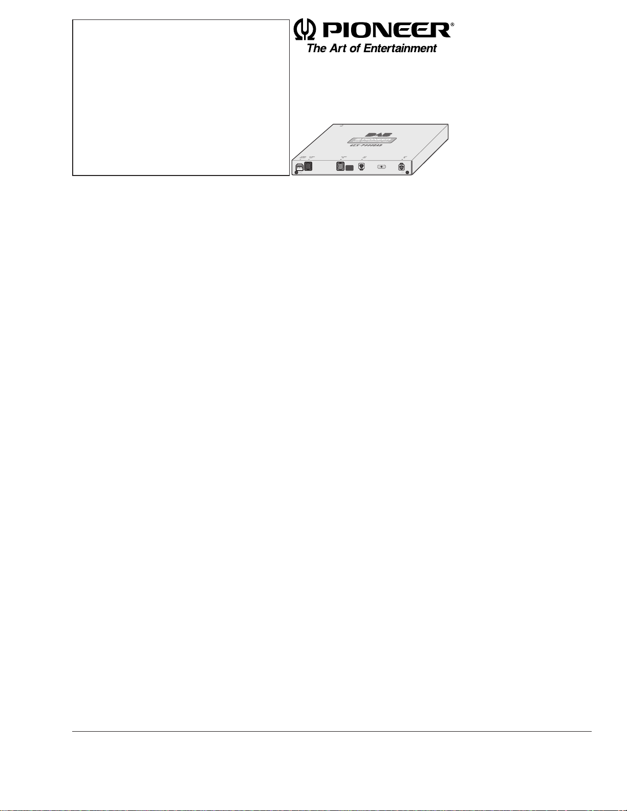
HIDE-AWAY DAB TUNER
GEX-P900DAB EW
CONTENTS
1. SAFETY INFORMATION ............................................2
2. EXPLODED VIEWS AND PARTS LIST.......................2
3. SCHEMATIC DIAGRAM .............................................6
4. PCB CONNECTION DIAGRAM ................................24
5. ELECTRICAL PARTS LIST ........................................28
6. ADJUSTMENT..........................................................35
7. GENERAL INFORMATION .......................................37
7.1 IC ........................................................................37
7.2 TEST MODE........................................................52
7.3 EXPLANATION ...................................................54
7.3.1 CIRCUIT DESCRIPTION ............................54
7.3.2 BLOCK DIAGRAM .....................................59
8. OPERATIONS AND SPECIFICATIONS.....................60
Se
r
vic
e
M
a
nu
a
l
Page 2
2
GEX-P900DAB
1. SAFETY INFORMATION
This service manual is intended for qualified service technicians; it is not meant for the casual do-it-yourselfer.
Qualified technicians have the necessary test equipment and tools, and have been trained to properly and safely repair
complex products such as those covered by this manual.
Improperly performed repairs can adversely affect the safety and reliability of the product and may void the warranty.
If you are not qualified to perform the repair of this product properly and safely; you should not risk trying to do so
and refer the repair to a qualified service technician.
2. EXPLODED VIEWS AND PARTS LIST
2.1 PACKING
9
5
11
4
2
3
16
18
8
7
6
6
12
13
10
14
1715
1
Page 3

3
GEX-P900DAB
1 Cord CDE5445
2 Screw BNC40P120FZK
* 3 Polyethylene Bag CEG1158
4 Screw HMF40P060FZK
5 Cord Clamper Assy CEA2444
6 Cord Clamper CNV5468
* 7 Polyethylene Bag E36-615
* 8 Polyethylene Bag CEG1101
9-1 Owner’s Manual CRD2721
9-2 Owner’s Manual CRD2722
9-3 Installation Manual CRD2723
* 9-4 Warranty Card CRY1087
9-5 Fastener(x2) CNM3728
9-6 Polyethylene Bag CEG1116
10 Polyethylene Bag CEG1190
11 Carton CHG3514
12 Contain Box CHL3514
13 Protector CHP2057
14 Protector CHP2058
15 Spacer CHW1713
16 Angle CNB2351
17 Antenna Assy CXB2841
18 Clamper CNV1343
Mark No. Description Part No. Mark No. Description Part No.
NOTE:
- Parts marked by “*”are generally unavailable because they are not in our Master Spare Parts List.
- Screws adjacent to ∇ mark on the product are used for disassembly.
- PACKING SECTION PARTS LIST
- Owner's Manual, Installation Manual
Part No. Language
CRD2721 English, Spanish, German
CRD2722 French, Italian, Dutch
CRD2723 English, Spanish, German,
French, Italian, Dutch
Page 4
4
GEX-P900DAB
2.2 EXTERIOR
Page 5

5
GEX-P900DAB
- EXTERIOR SECTION PARTS LIST
1 Screw BSZ26P060FMC
2 Screw BSZ30P060FMC
3 Screw BSZ30P060FZK
4 Plate CAH1654
5 Cord CDE5445
6 IC(IC803) PQ3RF23
7 IC(IC802) PQ30RV1
8 Screw HMF40P060FZK
9 Chassis CNA2014
10 Angle CNB2351
11 Case CNB2268
12 Shield CNC7513
13 Shield CNC7514
14 Shield CNC7515
15 Shield CNC7516
16 Transistor(Q803) 2SB945
17 IC(IC804) NJM7805FA
18 Insulator CNM5804
19 Terminal(CN802) CKF1059
20 Main Unit CWM5731
21 Screw BMZ26P060FMC
22 Nut CBN1026
23 Plug(CN801) CKS-460
24 Connector(CN222) CKS2104
25 Connector(CN221) CKS2600
26 Connector(CN262) CKS3409
27 Connector(CN261) CKS3414
28 Shield CNC7512
29 Holder CNC7518
30 Antenna Jack(CN401) CKX1059
31 Holder CNC7519
32 Holder CNC7517
33,34 •••••
35 Holder CNC7520
36 •••••
37 Screw ISS26P060FMC
Mark No. Description Part No. Mark No. Description Part No.
Page 6
6
GEX-P900DAB
A
1
234
B
C
D
12
34
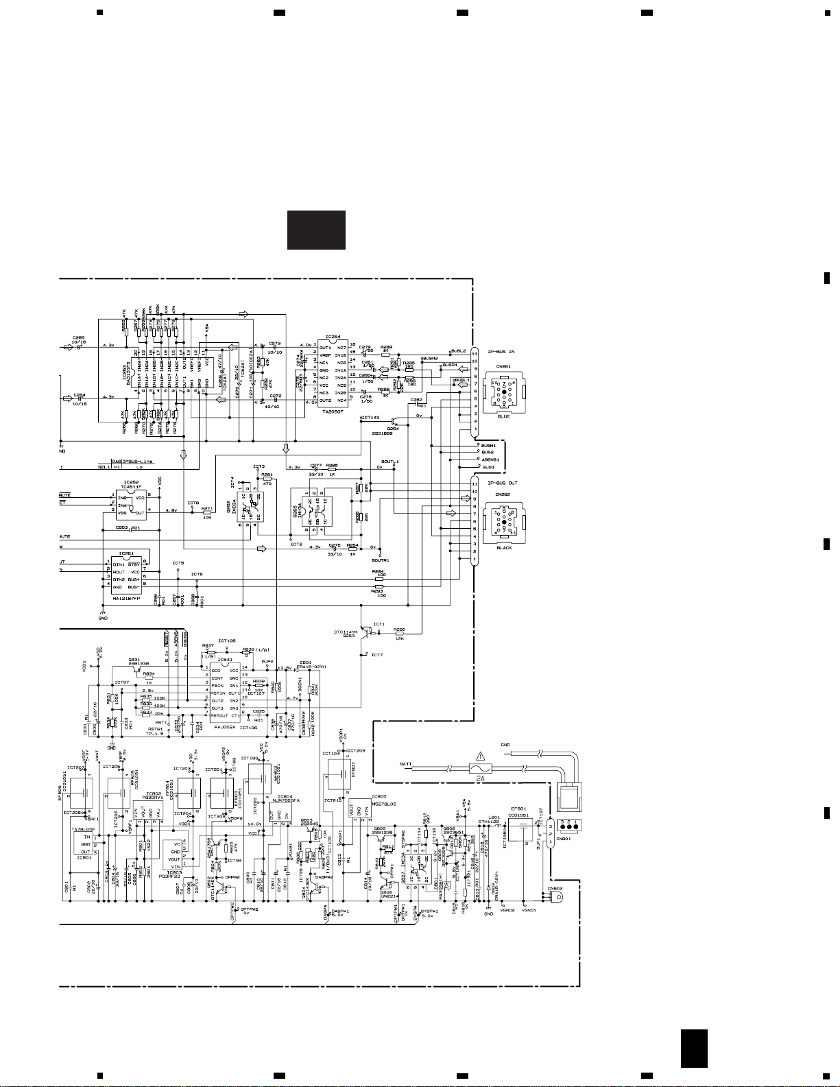
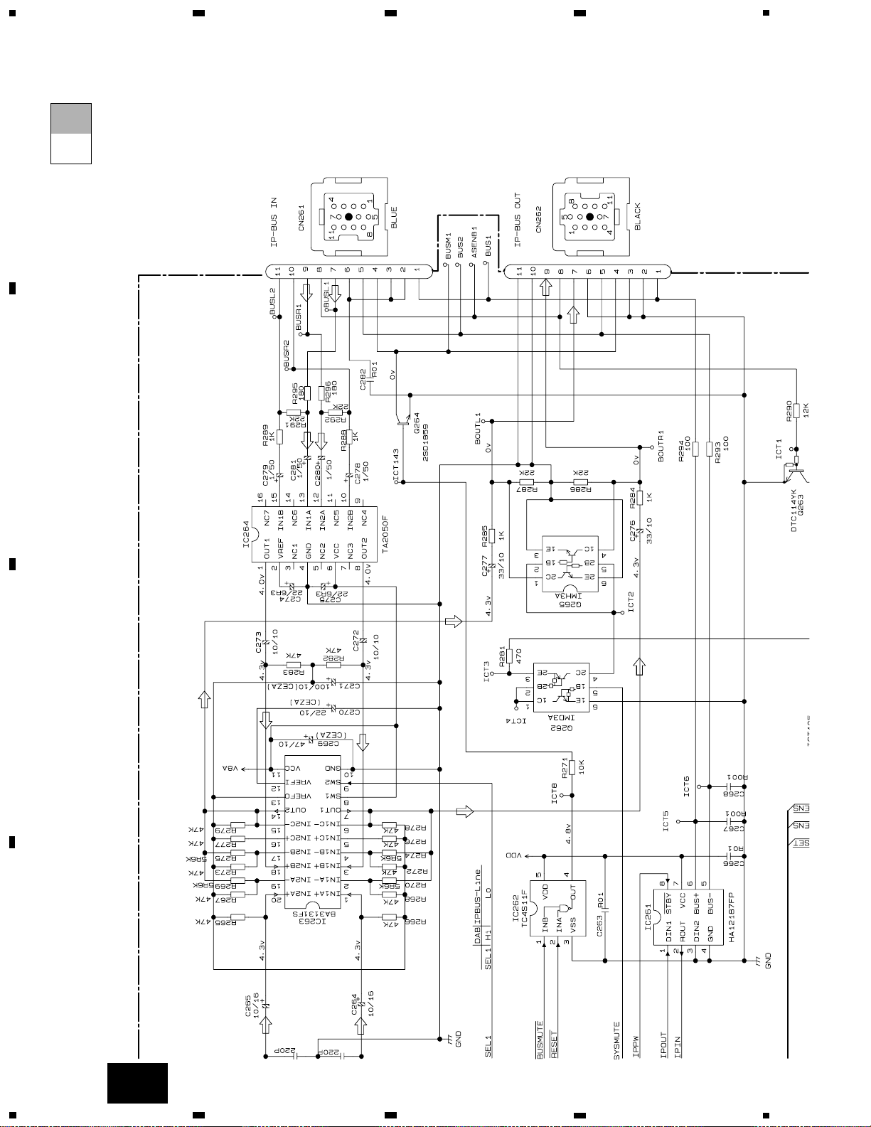
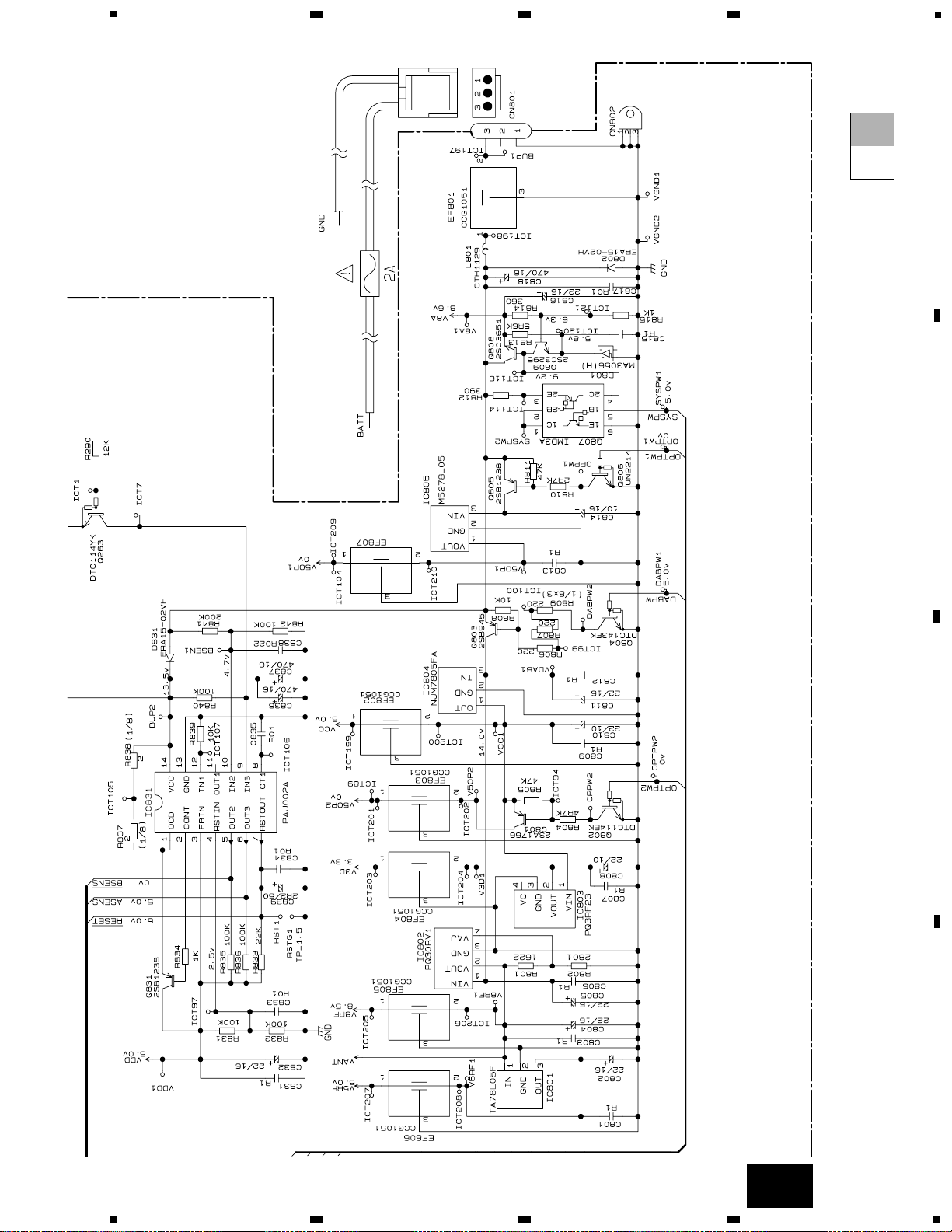
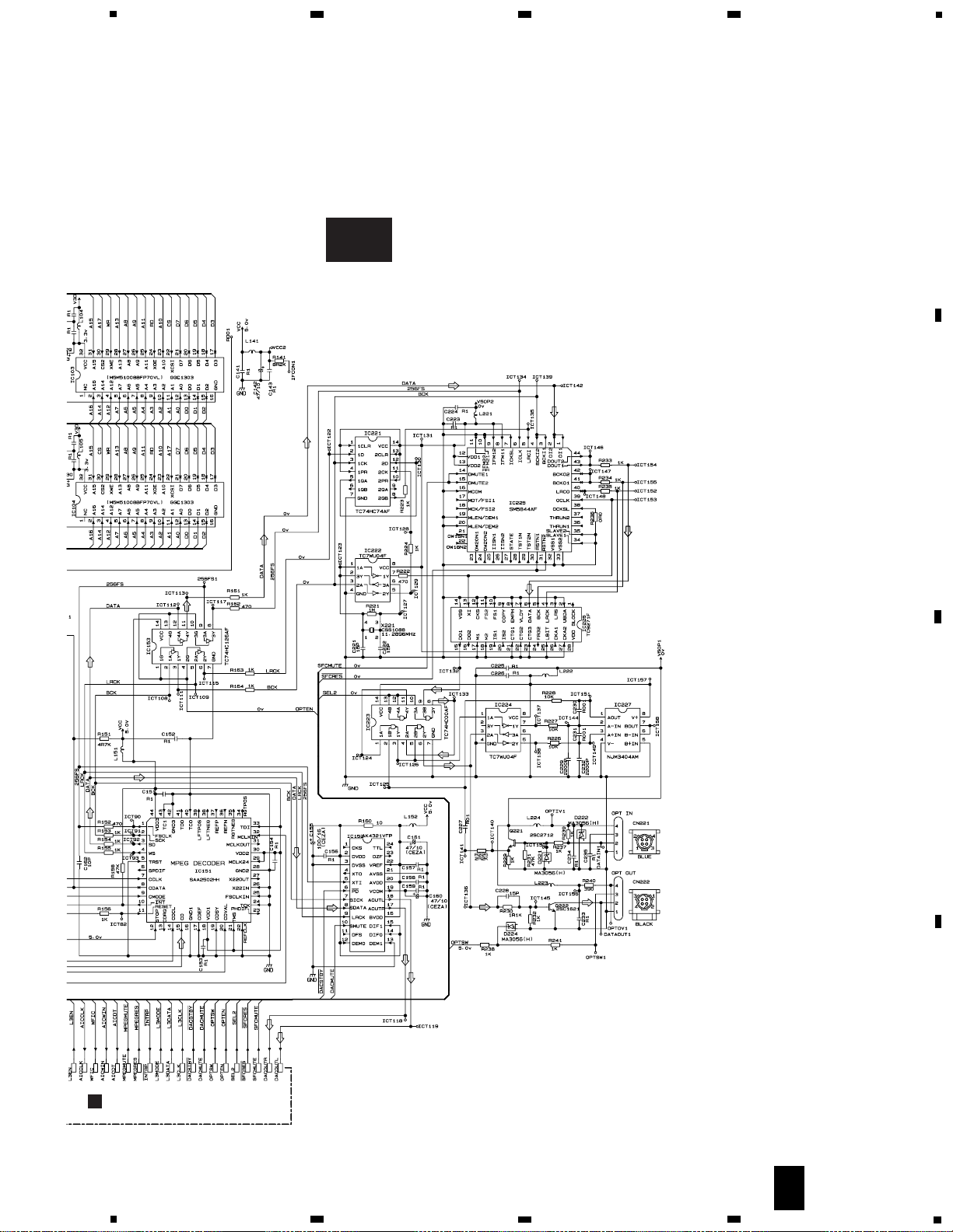
3. SCHEMATIC DIAGRAM
3.1 MAIN UNIT(1/3)
Note: When ordering service parts, be sure to refer to “EXPLODED VIEWS AND PARTS LIST” or “ELECTRICAL PARTS
LIST”.
SYSTEM CONTROL
RF SECTION
A
2/3
DIGITAL SECTION
A
3/3
A
1/3
A-a A-b
A-aA-a
A-b A-b
A-b A-b
A-a A-a
Large size
SCH diagram
Guide page
Detailed page
A-a
Page 7
7
GEX-P900DAB
5
6
7
8
A
B
C
D
5
6
7
8
SELECTOR
ISOLATOR
MUTE
POWER SUPPLY,
ASENSE,BSENSE
POWER SUPPLY
CEK1033
1.4mH
A
1/3
A-b
Page 8
8
GEX-P900DAB
DIGITAL SECTION
A
3/3
A
1
234
B
C
D
12
34
A-a
A-b
A-a
1/3
Page 9
9
GEX-P900DAB
SYSTEM CONTROL
RF SECTION
A
2/3
5
6
7
8
A
B
C
D
5
6
7
8
A-a
A-b
A-a
1/3
Page 10
10
GEX-P900DAB
SELECTOR
ISOLATOR
MUTE
POWER SUPPLY,
ASENSE,BSENSE
A
1
234
B
C
D
12
34
A-a
A-b
A-b
1/3
Page 11
11
GEX-P900DAB
POWER SUPPLY,
ASENSE,BSENSE
POWER SUPPLY
CEK1033
1.4mH
5
6
7
8
A
B
C
D
5
6
7
8
A-a
A-b
A-b
1/3
Page 12
12
GEX-P900DAB
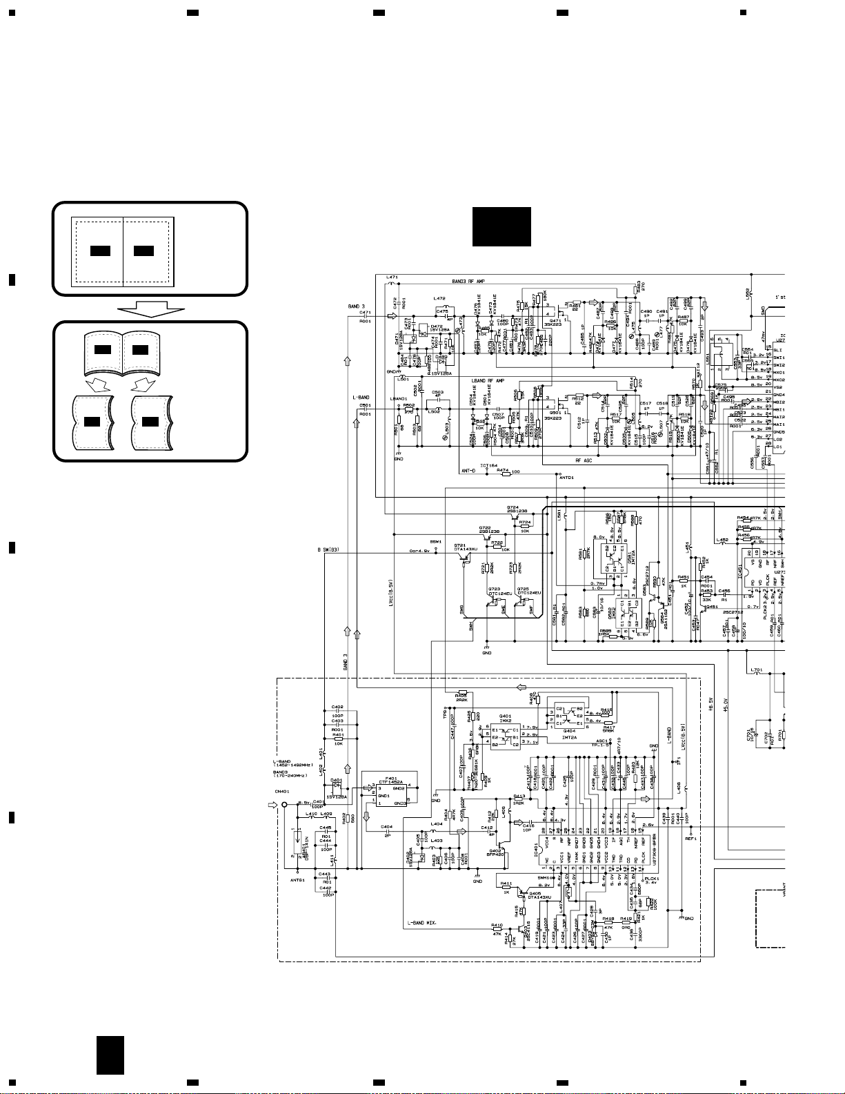
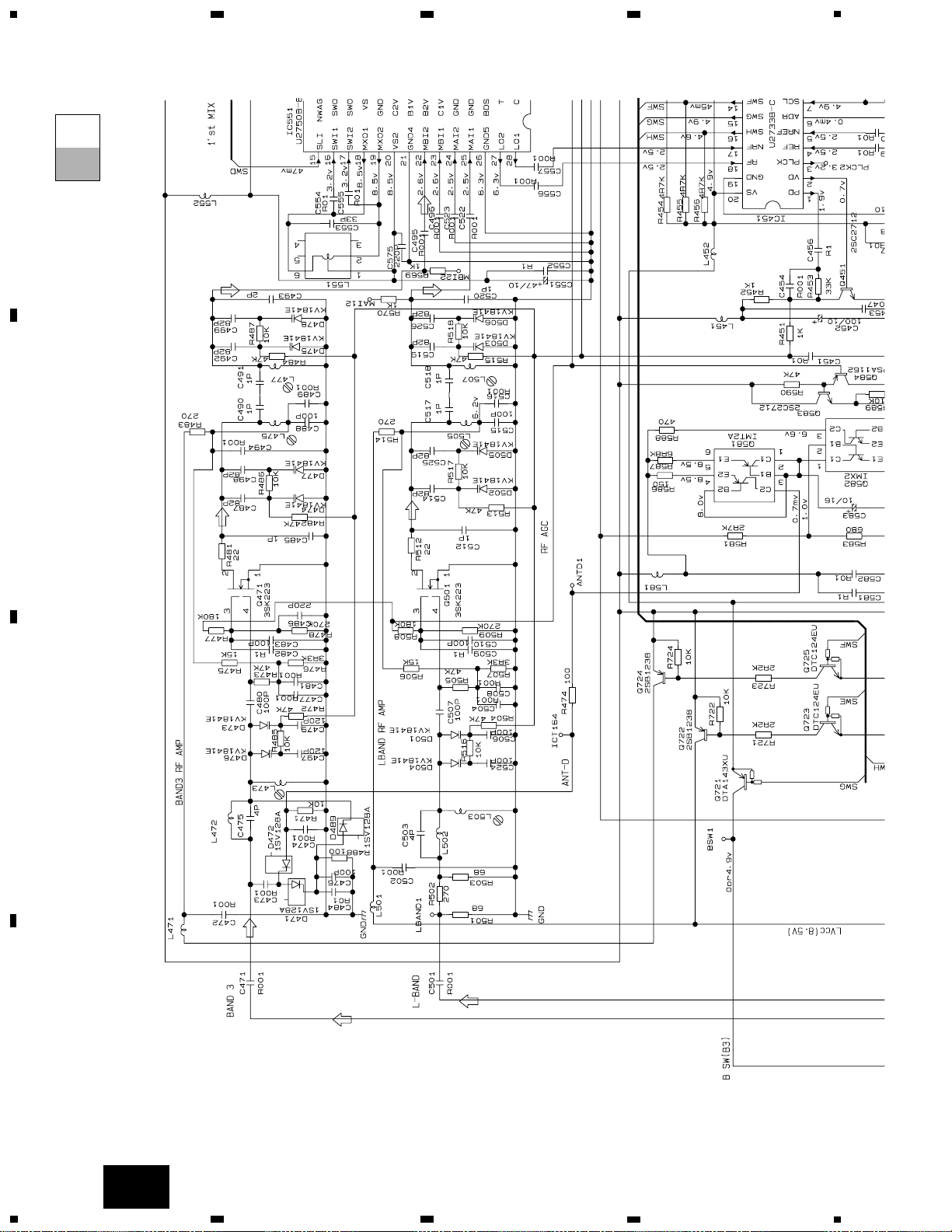
BAND3,RF AMP
L-BAND,RF AMP
ANT,DUMP
POWER SUPPLY
PL
L-BAND
DOWN CONVERTOR
A
1
234
B
C
D
12
34
A
2/3
3.2 MAIN UNIT(2/3)
A-a A-b
A-aA-a
A-b A-b
A-b A-b
A-a A-a
Large size
SCH diagram
Guide page
Detailed page
A-a
Page 13
13
GEX-P900DAB
5
6
7
8
A
B
C
D
5
6
7
8
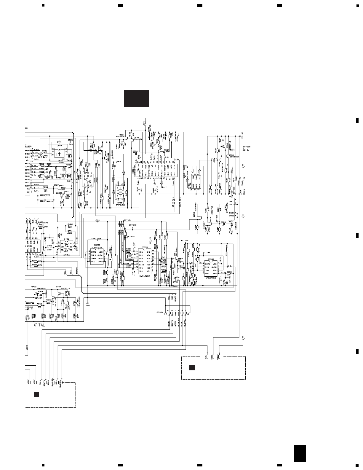
2nd MIXER
1st MIXER
SL
SAW FILTER
NULL DETECTOR
DIGITAL SECTION
A
3/3
A
1/3
A
2/3
A-b
Page 14
14
GEX-P900DAB
BAND3,RF AMP
L-BAND,RF AMP
ANT,DUMP
POWER SUPPLY
PLL
A
1
234
B
C
D
12
34
A-a
A-b
A-a
2/3
Page 15
15
GEX-P900DAB
L-BAND
DOWN CONVERTOR
5
6
7
8
A
B
C
D
5
6
7
8
A-a
A-b
A-a
2/3
Page 16
16
GEX-P900DAB
2nd MIXER
1st MIXER
PLL
SL
SAW FILTER
NULL DETECTOR
A
1
234
B
C
D
12
34
A-a
A-b
A-b
2/3
Page 17
17
GEX-P900DAB
DIGITAL SECTION
A
3/3
A
1/3
5
6
7
8
A
B
C
D
5
6
7
8
A-a
A-b
A-b
2/3
Page 18
18
GEX-P900DAB
A
1
234
B
C
D
12
34
DAB DECODER
VCXO
5V to 3.3V
LEVEL TRANSITION
CLOCK CONTROL
3.3V to 5V
LEVEL TRANSITION
CLOCK CONTROL
RF SECTION
A
2/3
A
3/3
3.3 MAIN UNIT(3/3)
A-a A-b
A-aA-a
A-b A-b
A-b A-b
A-a A-a
Large size
SCH diagram
Guide page
Detailed page
A-a
Page 19
19
GEX-P900DAB
5
6
7
8
A
B
C
D
5
6
7
8
SELECTOR
48/44.1kHz
CONVERSION
DIGITAL
INTERFACE
TRANSMITER
SELECTOR
DAC
OPT IN/OUT
A
1/3
A
3/3
A-b
Page 20

20
GEX-P900DAB
DAB DECODER
RF SECTION
A
2/3
A
1
234
B
C
D
12
34
A-a
A-b
A-a
3/3
Page 21

21
GEX-P900DAB
VCXO
5V to 3.3V
LEVEL TRANSITION
CLOCK CONTROL
3.3V to 5V
LEVEL TRANSITION
CLOCK CONTROL
A
5
6
7
8
A
B
C
D
5
6
7
A-a
A-b
A-a
3/3
8
Page 22

22
GEX-P900DAB
SELECTOR
48/44.1kHz
CONVERSION
DIGITAL
INTERFACE
TRANSMITER
A
1
234
B
C
D
12
34
A-a
A-b
A-b
3/3
Page 23

23
GEX-P900DAB
SELECTOR
DAC
OPT IN/OUT
A
1/3
5
6
7
8
A
B
C
D
5
6
7
8
A-a
A-b
A-b
3/3
Page 24

A
MAIN UNIT
24
GEX-P900DAB
A
1
234
B
C
D
12
34
4. PCB CONNECTION DIAGRAM
4.1 MAIN UNIT
A
Page 25

25
GEX-P900DAB
5
6
7
8
A
B
C
D
5
6
7
8
SIDE A
NOTE FOR PCB DIAGRAMS
1. The parts mounted on this PCB include all
necessary parts for several destination.
For further information for respective
destinations, be sure to check with the
schematic diagram.
2. Viewpoint of PCB diagrams
Capacitor
Connector
P.C.Board
Chip Part
SIDE A
SIDE B
A
Page 26

26
GEX-P900DAB
A
1
234
B
C
D
12
34
A
MAIN UNIT
A
Page 27

27
GEX-P900DAB
5
6
7
8
A
B
C
D
5
6
7
8
SIDE B
A
Page 28

28
GEX-P900DAB
Unit Number : CWM5731
Unit Name : Main Unit
MISCELLANEOUS
IC 101 IC MN6577H
IC 102 IC SAA3500
IC 103 (M5M51008BFP85VLL) GGC1312
IC 104 (M5M51008BFP85VLL) GGC1312
IC 151 IC SAA2502H
IC 152 IC AK4321VFP
IC 153 IC TC74HC126AF
IC 181 IC TC74HCT541AF
IC 182 IC TC7W00FU
IC 183 IC TC74LVX244FT
IC 184 IC TC7S00F
IC 185 IC TC7W74FU
IC 221 IC TC74HC74AF
IC 222 IC TC7WU04F
IC 223 IC TC74HC00AF
IC 224 IC TC7WU04F
IC 225 IC SM5844AF
IC 226 IC TC9271F
IC 227 IC NJM3404AM
IC 261 IC HA12187FP
IC 262 IC TC4S11F
IC 263 IC BA3131FS
IC 264 IC TA2050F
IC 351 IC NJM1496M
IC 352 IC UPC277G2
IC 391 IC NJM2904M
IC 401 IC U2730B-BFS
IC 451 IC U2733B-CFS
IC 531 IC U2759B-AFL
IC 551 IC U2750B-BFS
IC 601 IC PD5440A
IC 801 IC TA78L05F
IC 802 IC PQ30RV1
IC 803 IC PQ3RF23
IC 804 IC NJM7805FA
IC 805 IC M5278L05
IC 831 IC PAJ002A
Q 221 Transistor 2SC2712
Q 222 Transistor 2SC1621
Q 262 Transistor IMD3A
Q 263 Transistor DTC114YK
Q 264 Transistor 2SD1859
Q 265 Transistor IMH3A
Q 351 Transistor 2SC2712
Q 352 Transistor 2SC2712
Q 353 Transistor 2SC2712
Q 354 Transistor DTC124EU
Q 401 Transistor IMX2
Q 402 BFP420
Q 403 Transistor 2SC4116
Q 404 Transistor IMT2A
Q 405 Transistor DTA143XU
Q 451 Transistor 2SC2712
Q 452 Transistor IMH6A
Q 471 Transistor 3SK223
Q 501 Transistor 3SK223
Q 531 Transistor 2SC2712
Q 532 Transistor 2SA1162
Q 533 Transistor 2SC2712
Q 534 Transistor 2SC2712
Q 535 Transistor 2SC2712
Q 551 Transistor 2SC2712
Q 552 Transistor IMT2A
Q 553 Transistor 2SK1067
Q 554 Transistor 2SC4099
Q 581 Transistor IMT2A
Q 582 Transistor IMX2
Q 583 Transistor 2SC2712
Q 584 Transistor 2SA1162
Q 701 Transistor 2SC2712
Q 702 Transistor 2SC2712
Q 703 Transistor 2SC2712
Q 704 Transistor 2SC2712
Q 721 Transistor DTA143XU
Q 722 Transistor 2SB1238
Q 723 Transistor DTC124EU
Q 724 Transistor 2SB1238
Q 725 Transistor DTC124EU
Q 801 Transistor 2SA1766
Q 802 Transistor DTC114EK
Q 803 Transistor 2SB945
Q 804 Transistor DTC143EK
Q 805 Transistor 2SB1238
Q 806 Transistor UN2214
Q 807 Transistor IMD3A
Q 808 Transistor 2SC3651
Q 809 Transistor 2SC3295
Q 831 Transistor 2SB1238
D 221 Diode MA3056(H)
D 222 Diode MA3056(H)
D 224 Diode MA3056(H)
D 391 Diode MA8051(L)
D 401 Diode 1SV128A
D 402 Diode 1SV128A
D 403 Diode BBY52-03W
D 471 Diode 1SV128A
D 472 Diode 1SV128A
D 473 Diode KV1841E
D 474 Diode KV1841E
D 475 Diode KV1841E
D 476 Diode KV1841E
D 477 Diode KV1841E
D 478 Diode KV1841E
D 489 Diode 1SV128A
D 501 Diode KV1841E
5. ELECTRICAL PARTS LIST
NOTE:
- Parts whose parts numbers are omitted are subject to being not supplied.
- The part numbers shown below indicate chip components.
Chip Resistor
RS1/_S___J,RS1/__S___J
Chip Capacitor (except for CQS.....)
CKS....., CCS....., CSZS.....
=====Circuit Symbol and No.===Part Name Part No.
--- ------ ------------------------------------------ -------------------------
=====Circuit Symbol and No.===Part Name Part No.
--- ------ ------------------------------------------ -------------------------
A
Page 29

29
GEX-P900DAB
D 502 Diode KV1841E
D 503 Diode KV1841E
D 504 Diode KV1841E
D 505 Diode KV1841E
D 506 Diode KV1841E
D 551 Diode KV1841E
D 801 Diode MA3056(H)
D 802 Diode ERA15-02VH
D 831 Diode ERA15-02VH
L 101 Inductor CTF1295
L 102 Inductor CTF1295
L 103 Inductor CTF1295
L 104 Inductor CTF1295
L 105 Inductor CTF1295
L 141 Inductor CTF1295
L 151 Inductor CTF1295
L 152 Inductor CTF1295
L 181 Inductor CTF1295
L 182 Inductor CTF1295
L 183 Inductor CTF1295
L 184 Inductor CTF1295
L 221 Inductor CTF1295
L 222 Inductor CTF1295
L 223 Inductor CTF1295
L 224 Inductor CTF1295
L 391 Inductor CTF1295
L 401 Inductor LCYBR27J2125
L 402 Inductor LCYBR27J2125
L 403 Inductor LCYB15NJ1608
L 404 Inductor LCYB8N2K1608
L 406 Inductor LCYB3N3K1608
L 407 Coil CTX1067
L 408 Inductor CTF1295
L 409 Inductor LCYBR27J2125
L 410 Inductor LCYBR27J2125
L 411 Inductor LCTA100J3225
L 451 Inductor CTF1295
L 452 Inductor CTF1295
L 453 Inductor LCYB47NJ2125
L 454 Inductor LCYB47NJ2125
L 471 Inductor CTF1295
L 472 Coil CTJ1003
L 473 Coil CTJ1004
L 475 Coil CTJ1005
L 477 Coil CTJ1005
L 501 Inductor CTF1295
L 502 Coil CTJ1003
L 503 Coil CTJ1004
L 505 Coil CTJ1005
L 507 Coil CTJ1005
L 531 Inductor CTF1295
L 551 Coil CTE1135
L 552 Inductor CTF1295
L 553 Coil CTJ1006
L 554 Coil CTE1136
L 581 Inductor CTF1295
L 601 Inductor CTF1295
L 701 Inductor CTF1295
L 801 Choke Coil 1.4mH CTH1129
TH 407 Thermistor TN20-3E681K
CF 531 Filter CTF1447
CF 551 SAW Filter CTF1450
X 181 Resonator 24.576MHz CWX2266
X 221 Crystal Resonator 11.2896MHz CSS1088
X 601 Resonator 10.00MHz CSS1428
X 701 Resonator 18.432MHz CSS1440
VR 391 Semi-fixed 10kΩ(B) CCP1181
F 401 Filter CTF1452
F 351 Filter CTF1456
EF 351 CCG1086
EF 801 CCG1051
EF 802 CCG1051
EF 803 CCG1051
EF 804 CCG1051
EF 805 CCG1051
EF 806 CCG1051
EF 807 CCG1051
AR 401 DSP-141N
RESISTORS
R 101 RS1/10S4R7J
R 103 RS1/16S183J
R 105 RS1/16S123J
R 107 RS1/16S471J
R 108 RS1/16S471J
R 109 RS1/16S471J
R 110 RS1/16S471J
R 111 RS1/16S471J
R 112 RS1/16S471J
R 113 RS1/16S471J
R 114 RS1/16S471J
R 115 RS1/16S471J
R 116 RS1/16S471J
R 117 RS1/10S471J
R 120 RS1/10S473J
R 121 RS1/10S101J
R 122 RS1/10S102J
R 123 RS1/10S102J
R 124 RS1/10S102J
R 125 RS1/10S102J
R 126 RS1/10S102J
R 127 RS1/10S102J
R 128 RS1/10S102J
R 129 RS1/10S102J
R 130 RS1/16S102J
R 131 RS1/10S102J
R 132 RS1/10S0R0J
R 141 RS1/16S822J
R 151 RS1/16S472J
R 152 RS1/16S471J
R 153 RS1/16S102J
R 154 RS1/16S102J
R 155 RS1/16S102J
R 156 RS1/16S102J
R 158 RS1/16S473J
R 160 RS1/16S100J
R 161 RS1/16S102J
R 162 RS1/16S471J
R 163 RS1/16S102J
R 164 RS1/16S102J
R 181 RS1/16S101J
R 182 RS1/10S183J
R 184 RS1/16S101J
R 185 RS1/16S102J
R 186 RS1/16S102J
R 187 RS1/16S102J
R 188 RS1/16S102J
R 189 RS1/10S101J
R 190 RS1/10S102J
R 191 RS1/10S102J
=====Circuit Symbol and No.===Part Name Part No.
--- ------ ------------------------------------------ -------------------------
=====Circuit Symbol and No.===Part Name Part No.
--- ------ ------------------------------------------ -------------------------
Page 30

R 192 RS1/10S102J
R 193 RS1/10S102J
R 194 RS1/10S102J
R 195 RS1/10S102J
R 196 RS1/16S102J
R 221 RS1/16S105J
R 222 RS1/16S471J
R 223 RS1/16S102J
R 224 RS1/16S102J
R 225 RS1/16S222J
R 226 RS1/16S103J
R 227 RS1/16S103J
R 228 RS1/16S103J
R 229 RS1/16S102J
R 230 RS1/16S112J
R 231 RS1/16S473J
R 232 RS1/16S102J
R 233 RS1/16S102J
R 234 RS1/16S102J
R 235 RS1/16S102J
R 236 RS1/16S0R0J
R 237 RS1/10S102J
R 238 RS1/10S102J
R 239 RS1/10S102J
R 240 RS1/10S391J
R 241 RS1/10S102J
R 261 RS1/10S221J
R 262 RS1/10S221J
R 265 RS1/10S473J
R 266 RS1/10S473J
R 267 RS1/10S473J
R 268 RS1/10S473J
R 269 RS1/10S562J
R 270 RS1/10S562J
R 271 RS1/16S103J
R 272 RS1/10S473J
R 273 RS1/10S473J
R 274 RS1/10S562J
R 275 RS1/10S562J
R 276 RS1/10S473J
R 277 RS1/10S473J
R 278 RS1/10S473J
R 279 RS1/10S473J
R 281 RS1/16S471J
R 282 RS1/16S473J
R 283 RS1/16S473J
R 284 RS1/10S102J
R 285 RS1/10S102J
R 286 RS1/10S223J
R 287 RS1/10S223J
R 288 RS1/10S102J
R 289 RS1/10S102J
R 290 RS1/10S123J
R 291 RS1/10S223J
R 292 RS1/10S223J
R 293 RS1/10S101J
R 294 RS1/10S101J
R 295 RS1/10S181J
R 296 RS1/10S181J
R 351 RS1/16S103J
R 352 RS1/16S223J
R 353 RS1/16S183J
R 354 RS1/16S472J
R 355 RS1/16S101J
R 357 RS1/16S222J
R 358 RS1/16S222J
R 359 RS1/16S101J
R 360 RS1/16S0R0J
R 361 RS1/16S223J
R 362 RS1/16S222J
R 363 RS1/16S222J
R 364 RS1/16S183J
R 365 RS1/16S682J
R 366 RS1/16S102J
R 367 RS1/16S103J
R 368 RS1/16S104J
R 369 RS1/16S223J
R 370 RS1/16S183J
R 371 RS1/16S473J
R 372 RS1/16S123J
R 373 RS1/16S104J
R 374 RS1/16S103J
R 375 RS1/16S223J
R 376 RS1/16S223J
R 378 RS1/16S102J
R 379 RS1/16S102J
R 380 RS1/16S333J
R 381 RS1/16S123J
R 382 RS1/16S562J
R 383 RS1/16S152J
R 384 RS1/16S102J
R 392 RS1/16S103J
R 393 RS1/16S0R0J
R 394 RS1/16S222J
R 401 RS1/16S103J
R 402 RS1/16S561J
R 403 RS1/16S103J
R 404 RS1/16S472J
R 405 RS1/16S222J
R 406 RS1/16S682J
R 408 RS1/16S471J
R 409 RS1/16S102J
R 410 RS1/16S473J
R 411 RS1/16S102J
R 412 RS1/16S223J
R 413 RS1/16S122J
R 414 RS1/16S273J
R 415 RS1/16S473J
R 416 RS1/16S101J
R 417 RS1/16S562J
R 418 RS1/16S473J
R 419 RS1/16S0R0J
R 420 RS1/16S123J
R 421 RS1/16S102J
R 422 RS1/16S104J
R 426 RS1/16S221J
R 451 RS1/16S102J
R 452 RS1/16S102J
R 453 RS1/16S333J
R 454 RS1/16S472J
R 455 RS1/16S472J
R 456 RS1/16S472J
R 457 RS1/16S472J
R 458 RS1/16S472J
R 459 RS1/16S472J
R 460 RS1/16S472J
R 461 RS1/16S472J
R 462 RS1/16S103J
R 463 RS1/16S103J
R 471 RS1/16S103J
30
GEX-P900DAB
=====Circuit Symbol and No.===Part Name Part No.
--- ------ ------------------------------------------ -------------------------
=====Circuit Symbol and No.===Part Name Part No.
--- ------ ------------------------------------------ -------------------------
Page 31

R 472 RS1/16S473J
R 473 RS1/16S473J
R 474 RS1/16S101J
R 475 RS1/16S153J
R 476 RS1/16S332J
R 477 RS1/16S184J
R 478 RS1/16S274J
R 481 RS1/16S220J
R 482 RS1/16S473J
R 483 RS1/16S271J
R 484 RS1/16S473J
R 485 RS1/16S103J
R 486 RS1/16S103J
R 487 RS1/16S103J
R 488 RS1/16S101J
R 501 RS1/16S680J
R 502 RS1/16S271J
R 503 RS1/16S680J
R 504 RS1/16S473J
R 505 RS1/16S473J
R 506 RS1/16S153J
R 507 RS1/16S332J
R 508 RS1/16S184J
R 509 RS1/16S274J
R 512 RS1/16S220J
R 513 RS1/16S473J
R 514 RS1/16S271J
R 515 RS1/16S473J
R 516 RS1/16S103J
R 517 RS1/16S103J
R 518 RS1/16S103J
R 531 RS1/16S103J
R 533 RS1/16S473J
R 534 RS1/16S333J
R 535 RS1/16S0R0J
R 536 RS1/16S473J
R 537 RS1/16S333J
R 538 RS1/16S333J
R 539 RS1/16S102J
R 540 RS1/16S102J
R 541 RS1/16S333J
R 542 RS1/16S123J
R 543 RS1/16S302J
R 544 RS1/16S152J
R 545 RS1/16S102J
R 546 RS1/16S472J
R 551 RS1/16S271J
R 552 RS1/16S271J
R 553 RS1/16S103J
R 554 RS1/16S153J
R 555 RS1/16S473J
R 556 RS1/16S473J
R 557 RS1/16S472J
R 558 RS1/16S0R0J
R 559 RS1/16S392J
R 560 RS1/16S562J
R 561 RS1/16S0R0J
R 562 RS1/16S332J
R 563 RS1/16S103J
R 564 RS1/16S104J
R 565 RS1/16S104J
R 566 RS1/16S472J
R 567 RS1/16S471J
R 568 RS1/16S270J
R 569 RS1/16S102J
R 570 RS1/16S102J
R 581 RS1/16S272J
R 583 RS1/16S681J
R 585 RS1/16S152J
R 586 RS1/16S151J
R 587 RS1/16S682J
R 588 RS1/16S471J
R 589 RS1/16S103J
R 590 RS1/16S473J
R 601 RS1/16S470J
R 602 RS1/16S470J
R 603 RS1/16S470J
R 604 RS1/16S473J
R 606 RS1/10S473J
R 607 RS1/16S102J
R 608 RS1/10S472J
R 609 RS1/16S102J
R 610 RS1/16S102J
R 611 RS1/10S473J
R 612 RS1/10S473J
R 613 RS1/16S102J
R 614 RS1/16S102J
R 615 RS1/16S102J
R 616 RS1/16S102J
R 617 RS1/16S102J
R 618 RS1/16S101J
R 619 RS1/16S473J
R 620 RS1/16S473J
R 621 RS1/10S102J
R 622 RS1/10S102J
R 623 RS1/10S102J
R 625 RS1/16S0R0J
R 701 RS1/16S103J
R 702 RS1/16S103J
R 703 RS1/16S101J
R 704 RS1/16S101J
R 705 RS1/16S103J
R 706 RS1/16S122J
R 707 RS1/16S103J
R 708 RS1/16S103J
R 709 RS1/16S472J
R 710 RS1/16S472J
R 721 RS1/16S222J
R 722 RS1/16S103J
R 723 RS1/16S222J
R 724 RS1/16S103J
R 801 RS1/16S1622F
R 802 RS1/16S2801F
R 804 RS1/10S472J
R 805 RS1/10S473J
R 806 RS1/8S221J
R 807 RS1/8S221J
R 808 RS1/10S103J
R 809 RS1/8S221J
R 810 RS1/10S272J
R 811 RS1/10S473J
R 812 RS1/16S391J
R 813 RS1/10S562J
R 814 RS1/10S361J
R 815 RS1/10S102J
R 816 RS1/8S100J
R 831 RS1/16S104J
R 832 RS1/16S104J
R 833 RS1/16S223J
R 834 RS1/16S102J
31
GEX-P900DAB
=====Circuit Symbol and No.===Part Name Part No.
--- ------ ------------------------------------------ -------------------------
=====Circuit Symbol and No.===Part Name Part No.
--- ------ ------------------------------------------ -------------------------
Page 32

R 835 RS1/16S104J
R 836 RS1/16S104J
R 837 RS1/8S2R0J
R 838 RS1/8S2R0J
R 839 RS1/16S103J
R 840 RS1/16S104J
R 841 RS1/16S204J
R 842 RS1/16S104J
CAPACITORS
C 101 CKSQYB104K16
C 102 CEAS470M10
C 103 CKSQYB104K16
C 104 CKSQYB104K16
C 105 CKSQYB104K16
C 106 CKSQYB104K16
C 107 CKSQYB104K16
C 108 CEAS470M10
C 109 CKSRYB104K16
C 110 CKSQYB104K16
C 111 CKSQYB104K16
C 112 CEAS470M10
C 113 CKSQYB104K16
C 114 CEAS470M10
C 115 CKSQYB104K16
C 116 CKSQYB104K16
C 117 CKSQYB104K16
C 118 CKSQYB104K16
C 119 CKSQYB104K16
C 120 CKSQYB104K16
C 121 CKSRYB104K16
C 122 CKSRYB104K16
C 123 CKSRYB104K16
C 124 CKSRYB104K16
C 125 CKSRYB104K16
C 126 CCSQCH150J50
C 127 CCSQCH150J50
C 129 CEJA220M6R3
C 130 CEJA220M6R3
C 141 CKSRYB104K16
C 142 CEAS470M10
C 143 CKSRYB104K16
C 151 CKSRYB104K16
C 152 CKSRYB104K16
C 153 CKSRYB104K16
C 154 CKSRYB104K16
C 155 CEZA100M16
C 156 CKSRYB104K16
C 157 CKSRYB104K16
C 158 CKSRYB104K16
C 159 CKSRYB104K16
C 160 CEZA470M10
C 161 CEZA470M10
C 162 CCSQCH100J50
C 181 CKSRYB104K16
C 182 CKSRYB104K16
C 183 CKSQYB224K16
C 184 CKSQYB104K16
C 185 CKSQYB104K16
C 186 CKSQYB104K16
C 187 CKSQYB104K16
C 188 CKSRYB104K16
C 189 CKSRYB104K16
C 190 CCSQCH150J50
C 191 CCSQCH150J50
C 192 CCSQCH150J50
C 221 CCSRCH150J50
C 222 CCSRCH150J50
C 223 CKSRYB104K16
C 224 CKSRYB104K16
C 225 CKSRYB104K16
C 226 CKSRYB104K16
C 227 CKSRYB103K25
C 228 CCSRCH150J50
C 229 CKSRYB222K50
C 230 CKSRYB102K50
C 231 CKSRYB102K50
C 232 CKSRYB222K50
C 233 CKSQYB104K16
C 234 CKSQYB104K16
C 235 CKSQYB104K16
C 261 CCSRCH221J50
C 262 CCSRCH221J50
C 263 CKSRYB103K25
C 264 CEJA100M16
C 265 CEJA100M16
C 266 CKSRYB103K25
C 267 CKSRYB102K50
C 268 CKSRYB102K50
C 269 CEZA470M10
C 270 CEZA220M10
C 271 CEZA101M10
C 272 CEJANP100M10
C 273 CEJANP100M10
C 274 CEJA220M6R3
C 275 CEJA220M6R3
C 276 CEAS330M10
C 277 CEAS330M10
C 278 CEJA1R0M50
C 279 CEJA1R0M50
C 280 CEJA1R0M50
C 281 CEJA1R0M50
C 282 CKSQYB103K25
C 351 CKSRYB103K25
C 352 CKSRYB103K25
C 353 CKSRYB103K25
C 354 CKSRYB103K25
C 355 CKSRYB102K50
C 356 CKSRYB103K25
C 357 CKSRYB103K25
C 358 CEJANP2R2M35
C 359 CKSRYB103K25
C 360 CKSRYB103K25
C 362 CKSRYB103K25
C 363 CKSRYB104K16
C 364 CKSRYB152K50
C 391 CKSRYB103K25
C 401 CCSRCH101J50
C 402 CCSRCH101J50
C 403 CKSRYB102K50
C 404 CCSRCK2R0C50
C 405 CCSRCH101J50
C 406 CCSRCH101J50
C 407 CCSRCH101J50
C 408 CCSRCH102J25
C 409 CCSRCH101J50
C 412 CCSRCH4R0C50
C 416 CCSRCH100D50
C 417 CCSRCH101J50
C 418 CKSRYB102K50
32
GEX-P900DAB
=====Circuit Symbol and No.===Part Name Part No.
--- ------ ------------------------------------------ -------------------------
=====Circuit Symbol and No.===Part Name Part No.
--- ------ ------------------------------------------ -------------------------
Page 33

C 419 CKSRYB102K50
C 420 CCSRCH101J50
C 421 CCSRCH101J50
C 422 CKSRYB102K50
C 423 CKSRYB102K50
C 424 CCSRCH330J50
C 425 CCSRCH101J50
C 426 CCSRCH101J50
C 427 CKSRYB102K50
C 428 CCSRCJ3R0C50
C 429 CKSRYB102K50
C 430 CCSRCK1R0C50
C 431 CCSRCH101J50
C 432 CCSRCH101J50
C 433 CSZS4R7M10
C 434 CKSRYB681K50
C 435 CCSRCH680J50
C 436 CKSRYB332K50
C 437 CCSRCH101J50
C 438 CCSRCH101J50
C 439 CKSRYB102K50
C 440 CCSRCH101J50
C 442 CCSRCH101J50
C 443 CKSRYB103K25
C 444 CCSRCH101J50
C 445 CKSRYB103K25
C 446 CCSRCH101J50
C 447 CCSQCH101J50
C 451 CKSRYB103K25
C 452 CEAS101M10
C 453 CKSRYB473K16
C 454 CKSRYB102K50
C 456 CKSRYB104K16
C 457 CKSRYB103K25
C 458 CEAS101M10
C 459 CKSRYB103K25
C 460 CKSRYB103K25
C 461 CKSRYB103K25
C 462 CCSRCH181J50
C 471 CKSRYB102K50
C 472 CKSRYB102K50
C 473 CKSRYB102K50
C 474 CKSRYB102K50
C 475 CCSRCH4R0C50
C 476 CCSRCH101J50
C 477 CKSRYB102K50
C 479 CCSRCH121J50
C 480 CCSRCH101J50
C 481 CKSRYB102K50
C 482 CKSRYB104K16
C 483 CCSRCH101J50
C 484 CKSRYB103K25
C 485 CCSRCK1R0C50
C 486 CCSRCH221J50
C 487 CCSRCH820J50
C 488 CCSRCH101J50
C 489 CKSRYB102K50
C 490 CCSRCK1R0C50
C 491 CCSRCK1R0C50
C 492 CCSRCH820J50
C 493 CCSRCK2R0C50
C 494 CKSRYB102K50
C 495 CKSRYB102K50
C 496 CKSRYB102K50
C 497 CCSRCH121J50
C 498 CCSRCH820J50
C 499 CCSRCH820J50
C 501 CKSRYB102K50
C 502 CKSRYB102K50
C 503 CCSRCH4R0C50
C 504 CKSRYB102K50
C 506 CCSRCH101J50
C 507 CCSRCH101J50
C 508 CKSRYB102K50
C 509 CKSRYB104K16
C 510 CCSRCH101J50
C 512 CCSRCK1R0C50
C 514 CCSRCH820J50
C 515 CCSRCH101J50
C 516 CKSRYB102K50
C 517 CCSRCK1R0C50
C 518 CCSRCK1R0C50
C 519 CCSRCH820J50
C 520 CCSRCK1R0C50
C 522 CKSRYB102K50
C 523 CKSRYB102K50
C 524 CCSRCH101J50
C 525 CCSRCH820J50
C 526 CCSRCH820J50
C 531 CKSRYB103K25
C 532 CKSRYB103K25
C 533 CKSRYB103K25
C 534 CEAS220M16
C 535 CKSRYB103K25
C 536 CEJA4R7M35
C 537 CSZS1R0M16
C 538 CKSRYB104K16
C 539 CKSRYB104K16
C 540 CKSRYB103K25
C 541 CKSRYB103K25
C 542 CKSRYB104K16
C 543 CKSRYB104K16
C 544 CKSRYB102K50
C 545 CKSRYB104K16
C 546 CKSRYB104K16
C 551 CEAS470M10
C 552 CKSRYB104K16
C 553 CCSRCH330J50
C 554 CKSRYB103K25
C 555 CKSRYB103K25
C 556 CKSRYB102K50
C 557 CKSRYB102K50
C 558 CKSRYB103K25
C 559 CKSRYB103K25
C 560 CCSRCJ3R0C50
C 561 CCSRCK2R0C50
C 562 CCSRCJ3R0C50
C 563 CCSRCK2R0C50
C 564 CSZS3R3M10
C 565 CKSRYB102K50
C 566 CCSRCK2R0C50
C 567 CKSRYB102K50
C 568 CKSRYB103K25
C 569 CKSRYB103K25
C 570 CCSRCH390J50
C 571 CKSRYB103K25
C 572 CKSRYB103K25
C 573 CKSRYB103K25
C 575 CCSRCH221J50
C 576 CKSRYB102K50
33
GEX-P900DAB
=====Circuit Symbol and No.===Part Name Part No.
--- ------ ------------------------------------------ -------------------------
=====Circuit Symbol and No.===Part Name Part No.
--- ------ ------------------------------------------ -------------------------
Page 34

C 577 CKSRYB103K25
C 578 CEJA4R7M35
C 581 CKSRYB104K16
C 582 CKSRYB103K25
C 583 CEJA100M16
C 601 CKSRYB104K16
C 602 CKSQYB104K16
C 603 CKSQYB104K16
C 604 CKSQYB104K16
C 605 CKSRYB103K25
C 606 CEJA100M16
C 701 CEJA100M16
C 702 CKSRYB103K25
C 703 CKSRYB103K25
C 704 CCSRCH180J50
C 705 CCSRCH180J50
C 706 CCSRCH270J50
C 801 CKSRYB104K16
C 802 CEAS220M16
C 803 CKSRYB104K16
C 804 CEAS220M16
C 805 CEAS220M16
C 806 CKSQYB104K25
C 807 CKSRYB104K16
C 808 CEAS220M10
C 809 CKSRYB104K16
C 810 CEAS220M10
C 811 CEAS220M16
C 812 CKSQYB104K25
C 813 CKSRYB104K16
C 814 CEJA100M16
C 815 CKSRYB104K16
C 816 CEAS220M16
C 817 CKSQYB103K25
C 818 CEZA471M16
C 831 CKSRYB104K16
C 832 CSZST220M16
C 833 CKSRYB103K25
C 834 CKSRYB103K25
C 835 CKSRYB103K25
C 836 CEAS471M16
C 837 CEAS471M16
C 838 CKSRYB223K25
C 839 CEJA2R2M50
34
GEX-P900DAB
=====Circuit Symbol and No.===Part Name Part No.
--- ------ ------------------------------------------ -------------------------
Page 35

GEX-P900DAB
Equipment required:
• Head unit
• SG: Capable of outputting sine waves up to 1.5 GHz (no modulation function is required)
• DMM
• Adjustment stick (with flat tip)
1. VCO ADJUSTMENT
1) Connect the GEX-P900DAB to a DC regulated power supply. Connect the head unit and the GEX-P900DAB with an
IPBUS cable.
2) Set the power to ON, and enter DAB Service mode.
3) Set frequency to 13 F.
4) Check R556 on the side where P1 is located (the side not in contact with D551) with DMM (1) so that VT (tuning
voltage) can be measured. Adjust air-core coil (L553) so that VT is 7.00 V.
5) Set frequency to 5 A, and confirm that VT is within the range from 1.2 to 1.7 V.
L473
Pin 7
DMM(2)
L503
L475
L477
L505
L507
L553
R556
IC391
DMM(1)
MAIN UNIT
35
6. ADJUSTMENT
- Connection Diagram
Page 36

36
GEX-P900DAB
2. TRK (Tracking) ADJUSTMENT
1) Connect the GEX-P900DAB to a DC regulated power supply. Connect the head unit and the GEX-P900DAB with an
IPBUS cable.
2) Connect SG to ANT input.
3) Set the power to ON, and enter DAB Service mode.
4) BAND 3 ADJUSTMENT
Set frequency to 10 A. Set SG to 209.936 MHz and 35 dBuV. Then, check SLEVEL terminal (IC 391, Pin 7) with DMM
(2) so that SLEVEL voltage can be measured. Use the adjustment stick to adjust the air-core coil (L473) in front of
FET to maximum SLEVEL voltage. Similarly, adjust the air-core coil (L475) behind FET, as well as the air-core coil
(L477) behind L475. Repeat these adjustment steps several times to set SLEVEL voltage to maximum.
5) L-BAND ADJUSTMENT
Basic adjustment of L-Band is the same as adjustment of BAND 3. Set frequency to L12. Set SG to 1471.792 MHz
and 25 dBuV.
Use the adjustment stick to adjust the air-core coil (L503) in front of FET to maximum SLEVEL voltage. Similarly,
adjust the air-core coil (L505) behind FET, as well as the air-core coil (L507) behind L505. Repeat these adjustment
steps several times to set SLEVEL voltage to maximum.
- Confirmation of Operation
Equipment required:
• Head unit
• RF SG: Capable of outputting DAB signals up to 1.5 GHz (IQ modulation function is required)
• DAB encoder (e.g. KENWOOD DAB-3801)
1. Confirming Operation
1) Confirming BAND 3
Set the encoder to MODE 1.
Set the receiver and RF SG as shown below. Measure the error rate (see Note) to check whether the sensitivity
and maximum input of the specification are satisfied.
Receiver RF SG
5 A 174.928 MHz
10 A 209.936 MHz
13 F 239.200 MHz
2) Confirming L-BAND
Set the encoder to MODE 2.
Set the receiver and RF SG as shown below. Measure the error rate to check whether the sensitivity and maximum input of the specification are satisfied.
Receiver RF SG
L 1 1452.960 MHz
L12 1471.792 MHz
L23 1490.624 MHz
Note:
Error rate is evaluated at 1E-4 if the error rate after correction can be measured. To measure the error rate before correction, evaluation should be made at 5E-2.
The unit operates correctly if the specification is satisfied.
Page 37

GEX-P900DAB
7. GENERAL INFORMATION
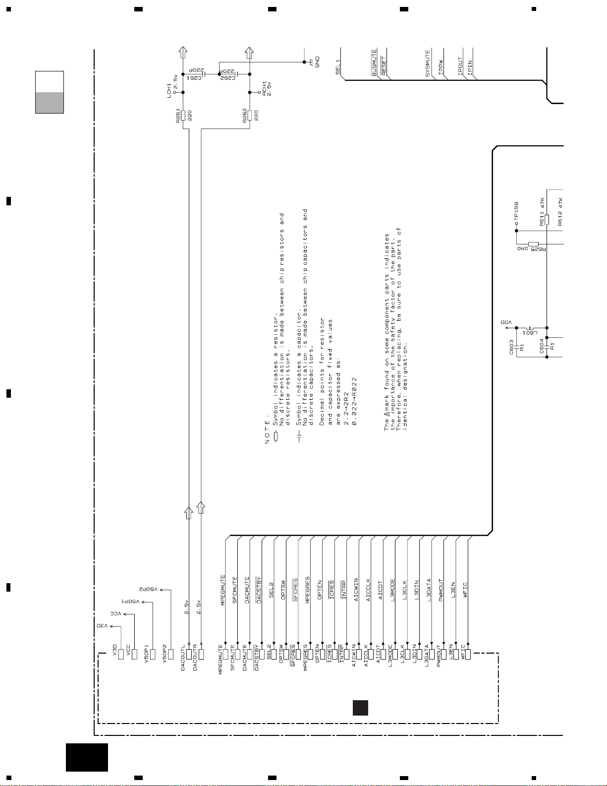
7.1 IC
MN6577H TC74LVX244FT U2730B-BFS
SAA3500 TC74HC74AF U2733B-CFS
GGC1312 (M5M51008BFP85VLL) TC7WU04F U2759B-AFL
SAA2502H TC74HC00AF U2750B-BFS
AK4321VFP SM5844AF PD5440A
TC74HC126AF TC9271F PQ30RV1
TC74HCT541AF NJM1496M PQ3RF23
TC7W00FU UPC277G2
- Pin Functions (MN6577H)
Pin No. Pin Name I/O Function and Operation
1-5 D0-D4 O Digital codes outputs D0 : LSB D9 : MSB
6 DVSS I Digital GND
7 DVDD I Digital power supply
8-12 D5-D9 O Digital codes outputs D0 : LSB D9 : MSB
13 TEST2 I L : Normal operation mode H : Test mode with built-in resistor
14 TEST1 I L : Normal operation mode H : Test mode with built-in resistor
15 DVDD I Digital power supply
16,17 DVSS I Digital GND
18 DVDD I Digital power supply
19 NC Not used
20 LINV I L : Normal output mode H : Inverted output from D8-D0
with built-in resistor
21 MINV I L : Normal output mode H : Inverted output from MSB(D9)
with built-in resistor
22 CLK I Clock input Performs sampling at the trailing edge of the clock.
Outputs digital codes at the leading edge of the 2.5th clock.
23 N0E I Digital output enable H : Digital output(D0-D9, OVF, UNDF) high-impedance
L : Digital output(D0-D9, OVF, UNDF)
24 POWD I H : Power down mode L : Normal operation mode
In power down mode, the UNDF terminal changes to "H" and other digital outputs
set to "L".
25,26 AVDD I Analog power supply
27 AVSS I Analog GND
28 NC Not used
29 VRTS O 1 When using 3.0V for VRT and 1.0V for VRB : connecting VRT to AVDD and
VRBS to VRB
2 When using 2.0V for VRT and 0V for VRB : connecting VRT to VRTS and VRB to
AVSS
30 VRT I TOP side reference voltage input
31-33 VR1-VR3 I Intermediate reference potential (capacity connection to AVSS)
34 VRB I Bottom side reference voltage input
35 VRBS O 1 When using 3.0V for VRT and 1.0V for VRB : connecting VRT to AVDD and
VRBS to VRB
2 When using 2.0V for VRT and 0V for VRB : connecting VRT to VRTS and VRB to
AVSS
36,37 NC Not used
38 AVDD I Analog power supply
39 VIN I Analog signal input
40-42 NC Not used
43 AVSS I Analog GND
44 DVSS I Digital GND
45 DVDD I Digital power supply
46 UNDF O Under flow output
47 OVF O Over flow output
48 NC Not used
37
Page 38

38
GEX-P900DAB
*MN6577H
- Pin Functions (SAA3500)
Pin No. Pin Name I/O Function and Operation
1,2 NC Connect to ground for proper operation.
3 GND1 Digital ground
4 OSC I System clock input 24.576 MHz
5 NC Do not connect !
6 VDD1 Voltage supply + 3V
7 GND2 Digital ground
8-17 INP[0-9] I 2 MHz IF of Baseband digital parallel input data (10 bits)
18 GND3 Digital ground
19 ADCLK O A/D clock output 8.192 MHz if BYP=high, 4.096 MHz if BYP=low.
20 IQSELECT I Clock signal indicating I or Q Baseband data if BYP=low.
Signal for swapping I and Q data bytes if BYP=high.
21 bypass I IF input stage bypass if BYP=low.
22 fsi I Frame sync Input (low indicates DAB null symbol detection).
23 fso O Frame sync output (low indicates DAB null symbol position)
24 AGC LOCK Not used
25 AGCW Not used
26 GND4 Digital ground
27 OCLK O Output data clock (negative edge indicates new data)
28 VDD2 Voltage supply + 3V
29 OIQ O Output I or Q select signal or frame trigger ( if OIQ=high)
30 ocir I Output select baseband if OIQ=1, CIR if OIQ=0
31 oen I OUT enable (if low)
32-39 OUT[0-7] O Baseband or channel impulse response output.
40 GND5 Digital ground
41 MCLK O Master clock output 24.576 MHz
42 VDD3 Voltage supply + 3V
43 REF O Receiver error flag (from viterbi decoder)
44-46 SOV3-1 O Serial output valid data 3-1
47,48 SOD3,2 O Serial output data 3,2
49 SOD1 O Serial output data 1 (from channel decoder)
12
13
24
25
37
48
1
36
IC's marked by* are MOS type.
Be careful in handling them because they are very
liable to be damaged by electrostatic induction.
Page 39

39
GEX-P900DAB
*SAA3500
30
31
50
81
100
1
80
51
Pin No. Pin Name I/O Function and Operation
50 SOC O Serial output clock (384 kHz continuous)
51 CFIC O µC interface signal indicating FIC processing
52 CMODE I µC interface mode input I2C or L3
53 CDATA I/O µC interface serial data I2C or L3 (5V compliant)
54 CCLK I µC interface clock input I2C or L3
55 reset I Chip reset input
56 SFCO O Simple full capacity output (direct from viterbi decoder)
57 RDC O Receiver data clock (6144 kHz continuous) or SFCO clock (burst)
58 rde I RDI output enable (if low)
59 RDO O Receiver data interface biphase output.
60 GND6 Digital ground
61 wr O Write data to RAM
62-68 A[17-11] O Address outputs external RAM
69 RD O Read data from RAM
70 CS O Chip select
71-78 D[7-0] I/O Data I/O external RAM
79 VDD4 Voltage supply + 3V
80 GND7 Digital ground
81-91 A[10-0] O Address outputs external RAM
92 TCO I Connect to ground for proper operation.
93 TDO O Not used
94 GND8 Digital ground
95 TCK I Boundary scan test clock input
96 TDI I Boundary scan test serial input
97 TMS I Boundary scan test mode select input
98 TRST I Boundary scan test reset input
99 TCI Not used
100 VCC Voltage supply + 3V
Page 40

40
GEX-P900DAB
NC
A16
A14
A5
A3
A2
A1
A0 DQ8
S1
A10
OE
A11
A9
A8
A13
W
S2
A15
Vcc
A4
1
2
3
4
5
6
7
8
9
10
11
12
32
31
30
29
28
27
26
25
24
23
22
21
13
14
15
16
20
19
18
17
DQ2
DQ3
GND
DQ4
DQ5
DQ6
DQ7
DQ1
A12
A7
A6
A0-A16:Address input
DQ1-DQ8:Data input/output
OE:Output enable input
S1,S2:Chip select input
W:Write control input
GND:Gnd
NC:Not used
VCC:Power supply
DIGITAL
TO
ANALOG
CONVERTER
PHASE
COMP.
DIVIDER
SPDIF
ENCODER
1
2
3
4
5
6
7
8
9
10
11
33
32
31
30
29
28
27
26
25
24
23
12
13
14
15
16
17
18
19
20
21
22
44
43
42
41
40
39
38
37
36
35
34
INPUT INTERFACE
DEQUANTIZATION AND SCALING
DECODING CONTROL
DEMULTI PLEXER
SYNTHESIS SUB-BAND FILTER
CLOCK GENERATORFSCLK
SCK
SD
WS
TRST
SPDIF
CCLK
CDATA
CMODE
INT
RESET PHDIF
TCK
FSCLKIN
X22IN
X22OUT
GND2
MCLK24
VDD2
MCLKOUT
MCLKIN
TDI
STOP
CDRQ
CDCL
CD
GND1
CDEF
VDD1
CDSY
CDVAL
TMS
REFCLK RGTPOS
RGTNEG
REFN
REFP
LFTNEG
LFTPOS
TC0
TDO
GND3
TC1
VDD3
SAA2502H
*GGC1312(M5M51008BFP85VLL)
Page 41

41
GEX-P900DAB
- Pin Functions (SAA2502H)
Pin No. Pin Name I/O Function and Operation
1 FSCLK O Sample rate clock output; buffered signal
2 SCK O Baseband audio data I2S clock output
3 SD O Baseband audio I2S data output
4 WS O Baseband audio data I2S word select output
5 TRST I Boundary scan test reset input
6 SPDIF O SPDIF baseband audio output
7 CCLK I L3 clock/I2C-bus bit clock input
8 CDATA I/O L3 data/I2C-bus serial data input/output
9 CMODE I L3 mode (address/data select input)
10 int O Interrupt request output; active LOW
11 RESET I Master reset input
12 STOP I Soft reset/stop decoding input
13 CDRQ O Coded data request output
14 CDCL I/O Coded data bit clock input/output
15 CD I MPEG coded data input
16 GND1 Ground 1
17 CDEF I Coded data error flag input
18 VDD1 Supply voltage 1
19 CDSY I Coded data byte or frame sync input
20 CDVAL I Coded data valid flag input
21 TMS I Boundary scan test mode select input
22 REFCLK I PLL reference clock input
23 PHDIF O PLL phase comparator output
24 TCK I Boundary scan test clock input
25 FSCLKIN I Sample rate clock input
26 X22IN I 22.579 MHz clock oscillator input or signal input
27 X22OUT O 22.579 MHz clock oscillator output
28 GND2 Ground 2
29 MCLK24 I Master clock frequency indication input
30 VDD2 Supply voltage 2
31 MCLKOUT O Master clock oscillator output
32 MCLKIN I Master clock oscillator input or signal input
33 TDI I Boundary scan test data input
34 RGTPOS O Analog right channel positive output
35 RGTNEG O Analog right channel negative output
36 REFN O Low reference voltage input for analog outputs
37 REFP O High reference voltage input for analog outputs
38 LFTNEG O Analog left channel negative output
39 LFTPOS O Analog left channel positive output
40 TC0 I Factory test scan chain control 0 input
Page 42

42
GEX-P900DAB
AK4321VFP
TC74HC126AF
TC74HCT541AF
Page 43

43
GEX-P900DAB
TC74HC74AF
TC7W00FU
VCC
1Y
2B
2A
8
7
6
5
1A
1B
2Y
GND
1
2
3
4
1
2
3
4
5
6
7
8
9
10
20
19
18
17
16
15
14
13
12
11
1G
1A1
2Y4
2Y2
2Y1
GND
2A1
1Y4
2A2
1Y3
2A3
1Y2
2A4
1Y1
2G
Vcc
1A4
1A2
2Y3
1A3
TC74LVX244FT
Page 44

44
GEX-P900DAB
DE-EMPHASIS ATT.
FILTER
SELECT
DATA
INTERFACE
SLAVE1
SLAVE2
OCLK
LRCO
BCKO1
BCKO2
DOUT1
DOUT2
OCKSL
THRUN1
THRUN2
RSTN1
TST1N
STATE
IISN1
VSS1
VSS2
IISN2
OW20N1
OW20N2
TST2N
DI1
DI2
BCKI1
BCKI2
IFM22
IFM21
IFM11
IFM12
ICLK
LRCI
ICKSL
MUTE
TIMING
CONTROLLER
DATA
INTERFACE
MODE
SWITCH
CLOCK
SELECT
TIMING
CONTROLLER
INPUT SIDE
DIVISION
12
13
14
15
16
17
18
19
20
21
22
44
43
42
41
40
39
38
37
36
35
34
11
10
9
8
7
6
5
4
3
2
23
24
25
26
27
28
29
30
31
32
33
1
FORMAT
CONTROLLER
DIRECT
MUTE
OUTPUT SIDE
DIVISION
OPERATIONAL CIRCUIT
DE-EMPHASIS
OPERATIONAL
ATT.
FILTER
OPERATIONAL
OUTPUT
OPERATIONAL
MCOM
DMUTE1
DMUTE2
VDD1
VDD2
MODE
MDT/FSI1
MCK/FSI2
MLEN/DEEM1
MLEN/DEEM2
OW18N1
OW18N2
LRCI BCKI DI
RSTN2
DITHER
TC7WU04F
TC74HC00AF
SM5844AF
Page 45

BLOCK
UBDA
LRS
VLDY
COPY
FS1
FS2
CKS M1
M2
XI
VSS DO1
DO2
IS1
IS2
CTG1
CTG2
CTG3
FR32
LBIT
CKA1
CKA2
VDD
EMPH
LRCK
BCK
DATA
DATA INPUT
CIRCUIT
CLOCK
GENERATOR
PARITY
GENERATOR
SERIAL
INTERFACE
BIFAZEMARK
MODULATOR
CATEGORY CODE
REGISTER
1
2
3
4
5
6
7
8
9
10
11
12
28
27
26
25
24
23
22
21
20
19
18
17
13
14
16
15
+
45
GEX-P900DAB
UPC277G2
1
3
2
OUT 1
Ii 1
IN 1
GND IN 2
Ii 2
OUT 2
V+
4
56
78
+
+
TC9271F
NJM1496M
1
2
3
4
5
6
7
14
13
12
11
10
9
8
(+) SIGNAL INPUT
GAIN ADJ.
GAIN ADJ.
NC
(+) CARRIER INPUT
NC
(–) CARRIER INPUT
NC
(–) OUTPUT
NC
V
–
(–) SIGNAL INPUT
BIAS
(+) OUTPUT
Page 46

46
GEX-P900DAB
- Pin Functions (U2730B-BFS)
Pin No. Pin Name I/O Function and Operation
1 NC Not used
2 C I Control input
3 VCC1 Supply voltage
4 VREF Reference pin of VCO
5 TANK Tank pin of VCO
6-8 GND Ground
9 VCC2 Supply voltage
10 TMD O Test output of main divider
11 TRD O Test output of reference divider
12 CD O Active filter output
13 PD O Three state charge pump output
14 PLCK O Lock indication output (open collector)
15 REF I Reference divider input
16 NREF I Reference divider input (inverted)
17 TH Threshold voltage of comperator
18 AGC I/O Charge pump output of comperator, AGC input for amplifier and mixer
19 IF O Intermediate frequency output
20 VCC3 Voltage supply
21-24 GND Ground
25 NRF I RF input (inverted)
26 RF I RF input
27 S I Control input
28 VCC4 Voltage supply
U2730B-BFS
NC
C
VCC1
VCC2
TMD
TRD
CD TH
AGC
PD
PLCK REF
NREF
IF
VCC3
GND
GND
GND
GND
NRF
RF
S
VCC4
GND
GND
GND
VREF
TANK
123456789101112
28 27 26 25 24 23 22 21 20 19 18 17
13 14
16 15
VCO
RF COUNTER
REFERENCE COUNTER
TEST INTERFACE
THREE STATE
PHASE
DETECTOR
PROG.
CHARGE PUMP
LOCK
DETECTOR
CONTROL INTERFACE
VOLTAGE STABILIZER
INTERNAL SUPPLY VOLTAGE
FOR THE SYNTHESIZER
Page 47

47
GEX-P900DAB
- Pin Functions (U2733B-CFS)
Pin No. Pin Name I/O Function and Operation
1 PD O Three-state charge pump output
2 VD O Active filter output
3 PLCK O Lock indicating output (open collector)
4 REF I Reference input
5 NREF I Reference input (inverted)
6 ADR Address selection
7 SCL Clock (I2C)
8 SDA Data (I2C)
9 NFDO O Frequency doubler output (inverted, open collector)
10 FDO O Frequency doubler output (open collector)
11 SWC O Switching output (open collector)
12 SWD O Switching output (open collector)
13 SWE O Switching output (open collector)
14 SWF O Switching output (open collector)
15 SWG O Switching output (open collector)
16 SWH O Switching output (open collector)
17 NRF I RF input (inverted)
18 RF I RF input
19 GND Ground
20 VS Supply voltage
U2733B-CFS
SWITCHES
7 BIT LATCH
MUX
MUX
FREQUENCY
DOUBLER x2
REFERENCE
COUNTER
FRACTIONAL
N CONTROL
PROG.
13 BIT COUNTER
:N,N+1
4 BIT LATCH
THREE STATE
PHASE
DETECTOR
12345678910
20 19 18 17 16 15 14 13 12 11
LOCK
DETECTOR
15 BIT LATCH
PROG.
CHARGE
PUMP
I2C BUS-INTERFACE/CONTROL
2 BIT
LATCH
VS
GND
RF
NRF
SWH
SWG
SWF
SWE
SWD
SWC
PD
VD
PLCK
REF
NREF
ADR
SCL
SDA
NFDO
FDO
Page 48

48
GEX-P900DAB
- Pin Functions (U2759B-AFL)
Pin No. Pin Name I/O Function and Operation
1 IF1IN I IF1 input
2 THRPRE I AGC-threshold for pre-amplifier
3 NC Not used
4 AGCPRE AGC for pre-amplifier
5 GND Ground
6 AGCT O AGC time constant for IF amplifier
7 NC Not used
8 IF2OUT O IF2 output
9-11 NC Not used
12,13 LO Local oscillator
14,15 NC Not used
16 THRIF I AGC threshold for IF amplifier
17 DC DC-level
18 VREF Reference voltage
19 BG Bandgap
20 VS Supply voltage
21,22 NC Not used
23 GND Ground
24 IF1IN I IF1 input
U2759B-AFL
1
2
3
4
5
6
7
8
9
10
11
12
24
23
22
21
20
19
18
17
16
15
14
13
BANDGAP
IF1IN
THRPRE
NC
NC
NC
NC
NC
LO LO
NC
NC
THRIF
DC
VREF
BG
VS
NC
NC
GND
IF1IN
IF2OUT
AGCPRE
GND
AGCT
Page 49

49
GEX-P900DAB
- Pin Functions (U2750B-BFS)
Pin No. Pin Name I/O Function and Operation
1 CP O Charge pump output of comparator
2 TH I Threshold input of comparator
3 BDSW I Band switch input
4,5 GND GND
6 C1VC Collector pin 1 of VCO
7 B2VC Base pin 2 of VCO
8 B1VC Base pin 1 of VCO
9 C2VC Collector pin 2 of VCO
10 GND GND
11 VS Supply voltage
12,13 SWO1,2 O Differential output of SAW-driver
14 NWAGC AGC mode selection
15 SLI AGC mode selection
16,17 SWI1,2 I Differential input of SAW-driver
18,19 MXO1,2 O Differential mixer output
20 VS Supply voltage
21 GND GND
22,23 MBI2,1 I Differential input of mixer B
24,25 MAI2,1 I Differential input of mixer A
26 GND GND
27,28 LO2,1 O Differential output of LO for PLL
U2750B-BFS
CP
TH
BDSW
B2VC
C2VC
GND
VS
SWO1 SWI2
MXO1
SWO2
NWAGC SL1
SWI1
MXO2
VS
GND
MBI2
MBI1
MAI2
MAI1
GND
LO2
LO1
B1VC
GND
GND
C1VC
123456789101112
28 27 26 25 24 23 22 21 20 19 18 17
13 14
16 15
VOLTAGE
STABILISATION
SAW-
DRIVER
BAND
SWITCH
VCO
C1 B2 B1 C2
BUF_LO
MIXA MIXB
Page 50

50
GEX-P900DAB
- Pin Functions (PD5440A)
Pin No. Pin Name I/O Function and Operation
1,2 NC Not used
3 DA1 Not used
4 DA0 Not used
5 NC Not used
6 NULLIN I NULL signal input
7 NC Not used
8 BYTE External data bus wides select input
9 CNVSS Processor mode select input
10,11 NC Not used
12 reset I Reset input
13 XOUT O Clock oscillation output
14 VSS1 Power supply
15 XIN Clock oscillation input (10MHz)
16 VCC1 Power supply
17 NMI I NMI input
18 CFIC I SAA3500 CFIC input
19 ASENS I Acc sense input (Acc-ON:H)
20 bsens I B.up sense input (B.up-ON:L)
21 IPIN1 I Connect to 29pin
22 IPPW O IP-BUS Power supply SW
23,24 NC Not used
25 L3EN O L3BUS input mode enable
26 PWMOUT O VCX0, PWM output
27,28 NC Not used
29 IPIN2 I IP-BUS input (KEYDISP input)
30 IPOUT O IP-BUS output (KEYDISP output)
31 L3OUT O L3BUS data output
32 L3IN I L3BUS data input
33 L3CLK O L3BUS clock output
34 L3MODE O L3BUS mode output
35 TxD O
36 AICDT I AIC data input
37 AICCLK I AIC clock input
38 AICWIN I AIC window input
39 int@%)@ I SAA2502 INTERRUPT
40 icreset O IC reset output (SAA3500)
41 OPTEN O Optical output enable
42 MPEGRES O IC reset output (SAA2502)
43 DABPW O DAB power supply SW
44 OPTPW2 O Optical power supply SW
45 OPTPW1 O Optical power supply SW
46 SYSPW O SYSTEM power supply SW
47 sfcres O IC reset output (SM5844)
48 DABMUTE O DAB mute output (non circuit)
49 SYSMUTE O SYSTEM mute output
50 busmute O BUS mute output
51 MODEL I Destination sense input
52 NC Not used
53 SEL2 O Audio selector (OPT)
54 SEL1 O Audio selector (IPBUS-line)
55 OPTSW I Light connector sense
56 dacstby O DAC power down
57 DACMUTE O DAC mute
58 SFCMUTE O SFC (SM5844) mute
59 MPEGMUTE O MPEG (SAA2502) mute
60,61 NC Not used
Page 51

51
GEX-P900DAB
*PD5440A
30
31
50
81
100
1
80
51
Pin No. Pin Name I/O Function and Operation
62 VCC2 Power supply
63 NC Not used
64 VSS4 Power supply
65-72 test&-test) I Testmode select SW
73-79 NC Not used
80 testin I Test input for manufacture line
81-88 MOUT 7-0 Not used
89 NC Not used
90 NULLSEL O NULL detect circuit select
91 I2C_DT O I2C data
92 I2C_CK O I2C clock
93,94 NC Not used
95 ANTSENS I Antenna terminal short detect
96 AVSS A-D power supply
97 SL I Signal level input
98 VREF A-D reference voltage input
99 AVCC A-D power supply
100 AGCW I AGC window input
PQ30RV1
VIN
VO
GND
VADJ
1
2 3 4
THERMAL
PROTECTOR
PROTECTOR
REFERENCE
VOLTAGE
+
-
PQ3RF23
VIN
VO
GND
VC
CONTROL
1
2 3 4
Page 52

52
GEX-P900DAB
7.2 TEST MODE
This unit is used together with a DAB control unit (e.g. DEX-P99R/EW, etc.). During Test mode, use the keys on the DAB
control unit.
All keys can be found on the remote control assembly, except the keys to enter Test mode.
• Entering Test mode:
Press the TA and Track Down keys simultaneously to reset the system.
• Exiting Test mode:
Set ACC to OFF.
- Keys used in Test mode
Left key Manual DOWN To receive a lower frequency block.
Right key Manual UP To receive a higher frequency block.
CH 1 Switches display. Normal display
↓
(Press the CH1 key.)
PLL IC communications checking display
↓
(After 2 seconds or when the CH 1 key is pressed)
SAA 3500 communications checking display
↓
(After 2 seconds or when the CH 1 key is pressed)
MPEG IC communications checking display
↓
(After 2 seconds or when the CH 1 key is pressed)
Test display
↓
(Press the CH 1 key.)
Returns to the normal display.
CH 2 Switches services. Same as the Service UP key.
CH 3 ARC ON/OFF Switches between ON and OFF of ARC.
Other keys are invalid.
- Display in Test mode:
1) PLL IC communications checking display
No problem was found: “PLL____OK”
A problem was found: “PLL____ERR”
2) SAA 3500 communications checking display
No problem was found: “DEC____OK”
A problem was found: “DEC____ERR”
3) MPEG IC communications checking display
No problem was found: “MPEG____OK”
A problem was found: “MPEG____ERR”
4) Test display
1st column 2nd column 3rd column 4th column 5th column 6th column 7th column 8th column
Page 53

53
GEX-P900DAB
• Estimated error rate of FIC
(1st column), (2nd column) (3rd column) E - (4th column)
• DAB mode
(5th column) 0 : Not identified.
1-4 : Transmission mode (DAB transmission mode)
• AFC detection
(6th column) 0 : AFC is not synchronized.
1 : AFC is synchronized.
• MPEG signal synchronous
(7th column) 0 : MPEG decoder is not synchronized.
1 : MPEG decoder is synchronized.
• MPEG signal error
(8th column) 0 : Normal
1 : Error in MPEG data.
Page 54

54
GEX-P900DAB
7.3 EXPLANATION
7.3.1 CIRCUIT DESCRIPTION
- What is DAB?
Digital Audio Broadcasting (DAB) is digital broadcasting for mobile communications using the MUSICAM (MPEG
Audio) audio compression system. The system was developed by the EUREKA 147 in Europe. For the digital modulation system, DAB uses Coded Orthogonal Frequency Division Multiplex (COFDM) based on multicarrier.
Internationally, DAB is also called as SYSTEM A in ITU-R.
Digital broadcasting may be called differently in some countries or areas. Even if the system is the same as DAB, it
may be called in different name.
DAR: Digital Audio Radio (IBOC, IBAC or DAB in the United States)
DRB: Digital Radio Broadcasting (DAB in Canada)
DSB: Digital Sound Broadcasting
- What is Coded OFDM?
Although OFDM technology has been known over years, it has recently attracted attention along with development of
FFT technology. In DAB, the system encodes and transmits signal.
1) Encoding is error correction using convolutional code. Compared with codes used in CDs (block code), convolutional code is more effective to handle random errors. Generally, it is called Viterbi decoding.
2) DAB signal requires wide band (1.54 MHz), and is given priority to be allocated to 12 channels of TV in Europe (5-13
channels under the standard). Also used is L-band (1.5 GHz).
Calculating based on band mode 2 will be: 4 KHz × 384 = 1.536 MHz Thus, 1.54 MHz.
Mode 1 1 KHz (1536) Band 3 (VHF) SFN (terrestrial)
Mode 4 2 KHz (768) L-Band (1.5 GHz) SFN (suggested by Canada)
Mode 2 4 KHz (384) L-Band (1.5 GHz) Local (terrestrial and satellite)
Mode 3 8 KHz (192) 3 GHz Cable
When DAB signal is allocated to TV 12 (approx. 7 MHz)
12A 12D12C12B
1.54MHz
Carrier interval: 1 KHz
Number of carriers: 1536
4-phase QPSK for every carrier
2 bits for every carrier
L-band VHF FFT
Viterbi
decoder
Musicam
DAB receiver
1452-1492MHz
174-240MHz
COFDM decoder
Page 55

55
GEX-P900DAB
- Why DAB is More Effective with Multipath Than FM?
Different from FM, DAB systems are designed under the conditions that multipath exists. DAB disperses the portion
that will be distorted by multipath, and corrects such part with error correction.
1) Frequency interleave
2) Time interleave
Portion containing error caused by multipath, etc. (digital data)
384ms
Changes burst error to random error by the time axis.
Corrects error by Viterbi decoding.
Received signal (1.54 MHz)
Reallocation of frequency after FFT
Distorted portion by multipath, etc.
Disperses distorted carriers by frequency
interleave to change them as random error.
Page 56

56
GEX-P900DAB
3) Guard interval
The time 25% more than the sampling time required for processing DAB signals by FFT is called "guard interval." For
multipath within the time of guard interval, errors can be corrected in most cases, regardless of the D/U ratio.
Mode 1 2048 points (1 ms): Number of samples required for FFT
512 points (250 µs): Guard interval
The time of guard interval depends on modes. Different time of guide interval is used for transmitting frequency,
receiving speed (vehicle speed), etc.
S1 S2
S1 S2
Actual DAB signal
Interference between
different symbols
(effect of delay)
Time required for FFT
(1 ms)
Guard interval (250 µs)
Received DAB signal
S1 S2
Time required for FFT for every symbol
Delayed multipath wave
Direct wave
(OFDM wave)
Page 57

57
GEX-P900DAB
- What is SFN?
Single Frequency Network (SFN) functions in the same way as with Network Follow (NF) of RDS. The principle of SFN
uses the advantage of DAB that signals can be received for multipath having delay within the time of guide interval.
1) Different from FM, all transmitting antennas use the same frequency in SFN. Thus, completely muteless status can
be achieved in NF.
2) SFN receives frequency from several antennas simultaneously. Thus, network gain may be obtained by several dBs.
Viewing from the receiver, both SFN and mutipath behave in the same manner.
antenna 1
102.2MHz
antenna 2
89.6MHz
antenna 3
106.8MHz
antenna 1
225MHz
antenna 3
225MHz
antenna 2
225MHz
DAB systemFM system
Multipath
SFN
Link
Page 58

58
GEX-P900DAB
- Broadcasting Content
DAB can be considered as a system that can transmit the conventional seven broadcasting stations using a single
broadcasting wave. New styles of broadcasting can be offered by replacing the content of broadcasting in audio signals with data.
1) Currently, audio quality equivalent to CD for a maximum of seven channels and RDS data of upward compatibility
are transmitted. The capacity of every channel can be quickly changed by technology called "Dynamic
Reconfiguration," thus can increase the number of channels.
2) DAB has transmission capacity of a maximum of 1.7 Mbps (larger than Video CD), thus various types of data can be
transmitted.
3) We are planning to transmit navigation-related data, such as DGPS and TMC, in the future. The DAB signal itself has
a simple system to detect its own position (TII: Transmitter Identification Information), implying a possibility of simplified navigation.
Actual selection of service using a DAB receiver will be as the illustration shown below
(a large display is required).
Currently, use of the DAB standard in future is examined in public organizations in Europe and other areas, including
EUREKA 147, WorldDAB, EACEM, CENELEC, ETSI, and CEPT.
The latest information on DAB can be obtained from home page (http://www.kp.dlr.de/DAB/) via the Internet. The content is shown as a menu that links to detailed information.
Service Menu
-Radio1
-Radio2
-Network East
-Sound 2000
Language
-German
-English
-French
-Dutch
Programme type
-News
-Classics
-Pop Music
-Education
Page 59

59
GEX-P900DAB
7.3.2 BLOCK DIAGRAM
A
Page 60

60
GEX-P900DAB
8. OPERATIONS AND SPECIFICATIONS
- Connection Diagram
5. IP-BUS Output
(Black)
12.Head Unit
(sold separately)
3. This Unit
1. Antenna Unit
2. Antenna Input
4. Power Supply
6. IP-BUS Input
(Blue)
7. Not used. (Optical Output (Black))
8. Not used. (Optical
Input (Blue))
9. IP-BUS cable
10.To IP-BUS Input
(Blue)
11.Multi-CD player
(sold separately)
14.Orange
Toterminal always supplied with power
regardless of ignition switch position.
15.Black (ground)
Tovehicle (metal) body.
13.Fuse holder
Page 61

61
GEX-P900DAB
Key Finder
Head Unit (e.g. DEH-P945R)
Remote Controller (e.g. DEH-P945R)
Steering Remote Controller:
• You can operate in the same way with the Steering Remote Controller
supplied with the Head Unit. For details, refer to the Head Unit’s
Operation Manual.
Buttons 1– 6
+/– button
[/] button
BAND button
FUNCTION button
TUNER/DAB button
PGM button
DISPLAY button
'/ button
PTY button
+/– button
PTY button [/] button
TAbutton '/ button
SOURCE/OFF button
DISPLAY button
'
'
Page 62

62
GEX-P900DAB
About the “DAB READY” Indicator
There’s a “DAB READY” indicator in the Head Unit’s display. This indi-
cates DAB reception is possible.
Note:
• Head Unit Group 2 and 3 units do not feature a “DAB READY” indicator.
When listening to DAB
Lights during Ensemble reception.
When listening to a non-DAB source
Lights when in an area where DAB reception is possible.
Switching Power ON/OFF
• Select DAB.
Head Unit
Press the SOURCE/OFF button, and select DAB as follows.
Built-in CD Player → Tuner →DAB (Digital Audio Broadcasting) →
Multi-MD Player → Multi-CD Player → AUX → ...
To switch the sources OFF, hold down the SOURCE/OFF button for 1 sec-
ond or more.
Remote Controller
Press the TUNER/DAB button, and select DAB as follows.
Tuner → DAB (Digital Audio Broadcasting) → OFF
“DAB READY”
Basic Operation
Basic Operation of DAB
1. Select DAB.
When you first switch to DAB, Auto Seek is performed to find the highest
Ensemble frequency. (Auto Seek is also performed in the same way each
time you switch bands.)
Once Ensemble is received, Auto Seek ends.
2. Select a desired Service.
If you cannot find a desired Service, repeat step 2 after switching to
Ensemble in step 3.
3. Tune to a high or low frequency (Ensemble).
4. Turn the source OFF.
Hold for 1 second
Hold for 0.5 secondsHold for 0.5 seconds
Each press
changes the Source ...
Each press
changes the Source ...
Page 63

63
GEX-P900DAB
Selecting the Ensemble
You can switch to an Ensemble offering a desired Service.
• Tune to a high or low frequency (Ensemble).
By pressing the same button, search stops and the unit switches to standby
for reception of that Ensemble frequency.
Note:
• The initial Language Filter setting is OFF.
Language Filter OFF
Priority is given to the first Service in a received Ensemble. After it is
selected, sound of that Service’s Primary Service Component is output.
Language Filter ON
Search for a Service Component of the set language among the received
Ensemble is performed.
- When a Service Component is found
Sound of that Service Component is output.
- When a Service Component is not found
Priority is given to the first Service. After it is selected, sound of that
Service’s Primary Service Component is output.
Hold for 0.5 secondsHold for 0.5 seconds
Basic Operation Specifications
General
Power source .......... 14.4 V DC (10.8 – 15.1 V allowable)
Grounding system ........................................ Negative type
Max. current consumption ........................................ 0.6 A
Dimensions .................... 231 (W) ×28 (H) × 182 (D) mm
Weight ...................................................................... 2.5 kg
DAB tuner
Frequency range
(Band “) .......... 174.928 – 239.200 MHz (5A – 13F)
(L Band) .... 1,452.960 – 1,490.624 MHz (L1 – L23)
Usable sensitivity
(Band “) .................................................. – 100 dBm
(L Band) .................................................. – 97.5 dBm
Mode .................................................................. –, —, “, ”
Audio
Signal-to-noise ratio .................... 94 dB (IEC-A network)
Separation .................................................... 94 dB (1 kHz)
Antenna
Type .................................................................. Active type
Note:
• Specifications and the design are subject to possi-
ble modification without notice due to improve-
ments.
 Loading...