

Page 1
ORDER NO.
CRT3424
GEX-P10XMT/XN/UC
XM DIGITAL SATELLITE DATA & AUDIO RECEIVER
GEX-P10XMT
- Caution
• When users complain "No Signal" is displayed, there is a possibility that an installed XM antenna
cable has shorted out only occasionally.
If there are no problems in the main tuner by a service-man checking or NTF is used, let users
confirm that the XM antenna cable has no short-circuit.
• Connect the Acc lead of the Cord Assy (CDE8009) only when IP-BUS is not connected.
/XN/UC
For details, refer to "Important Check Points for Good Servicing".
PIONEER CORPORATION 4-1, Meguro 1-chome, Meguro-ku, Tokyo 153-8654, Japan
PIONEER ELECTRONICS (USA) INC. P.O. Box 1760, Long Beach, CA 90801-1760, U.S.A.
PIONEER EUROPE NV Haven 1087, Keetberglaan 1, 9120 Melsele, Belgium
PIONEER ELECTRONICS ASIACENTRE PTE. LTD. 253 Alexandra Road, #04-01, Singapore 159936
PIONEER CORPORATION 2005
K-ZZW. FEB. 2005 Printed in Japan
Page 2
CAUTIO
e
r
ect
thend
d
the
to
the
d
g
to
ARNING
eadlde
d
ta
ectrica
to
the
5
1234
SAFETY INFORMATION
A
This service manual is intended for qualified service technicians; it is not meant for the casual do-it-yourself
Qualified technicians have the necessary test equipment and tools, and have been trained to properly and safely repai
erformed
ou
renotualified
ARNING
Thisroduct
B
Health & Safety Code Section 25249.6 - Proposition 6
ntainsl
n adversely
r
- Service Precautions
1. You should conform to the regulations governing the product (safety, radio and noise, and other regulations),
and should keep the safety during servicing by following the safety instructions described in this manual.
C
repair
n
ff
thisroduct
in
l
reliability theroduct
roperlyn
l
arts
ntain
ndmayvoi
ou
houldnotrisktryin
hemicalswhich rknown
D
E
F
2
1234
GEX-P10XMT/XN/UC
Page 3
5678
[Important Check Points for Good Servicing]
In this manual, procedures that must be performed during repairs are marked with the below symbol.
Please be sure to confirm and follow these procedures.
1. Product safety
Please conform to product regulations (such as safety and radiation regulations), and maintain a safe servicing environment by
following the safety instructions described in this manual.
1 Use specified parts for repair.
Use genuine parts. Be sure to use important parts for safety.
2 Do not perform modifications without proper instructions.
Please follow the specified safety methods when modification(addition/change of parts) is required due to interferences such as
radio/TV interference and foreign noise.
3 Make sure the soldering of repaired locations is properly performed.
When you solder while repairing, please be sure that there are no cold solder and other debris.
Soldering should be finished with the proper quantity. (Refer to the example)
4 Make sure the screws are tightly fastened.
Please be sure that all screws are fastened, and that there are no loose screws.
5 Make sure each connectors are correctly inserted.
Please be sure that all connectors are inserted, and that there are no imperfect insertion.
6 Make sure the wiring cables are set to their original state.
Please replace the wiring and cables to the original state after repairs.
In addition, be sure that there are no pinched wires, etc.
7 Make sure screws and soldering scraps do not remain inside the product.
Please check that neither solder debris nor screws remain inside the product.
8 There should be no semi-broken wires, scratches, melting, etc. on the coating of the power cord.
Damaged power cords may lead to fire accidents, so please be sure that there are no damages.
If you find a damaged power cord, please exchange it with a suitable one.
9 There should be no spark traces or similar marks on the power plug.
When spark traces or similar marks are found on the power supply plug, please check the connection and advise on secure
connections and suitable usage. Please exchange the power cord if necessary.
0 Safe environment should be secured during servicing.
When you perform repairs, please pay attention to static electricity, furniture, household articles, etc. in order to prevent injuries.
Please pay attention to your surroundings and repair safely.
A
B
C
D
2. Adjustments
To keep the original performance of the products, optimum adjustments and confirmation of characteristics within specification.
Adjustments should be performed in accordance with the procedures/instructions described in this manual.
3. Lubricants, Glues, and Replacement parts
Use grease and adhesives that are equal to the specified substance.
Make sure the proper amount is applied.
4. Cleaning
For parts that require cleaning, such as optical pickups, tape deck heads, lenses and mirrors used in projection monitors, proper
cleaning should be performed to restore their performances.
5. Shipping mode and Shipping screws
To protect products from damages or failures during transit, the shipping mode should be set or the shipping screws should be
installed before shipment. Please be sure to follow this method especially if it is specified in this manual.
56
GEX-P10XMT/XN/UC
E
F
7
8
3
Page 4

1234
CONTENTS
SAFETY INFORMATION.....................................................................................................................................2
1. SPECIFICATIONS............................................................................................................................................ 5
2. EXPLODED VIEWS AND PARTS LIST ............................................................................................................6
A
B
2.1 PACKING ................................................................................................................................................... 6
2.2 EXTERIOR................................................................................................................................................. 8
3. BLOCK DIAGRAM AND SCHEMATIC DIAGRAM..........................................................................................10
3.1 BLOCK DIAGRAM................................................................................................................................... 10
3.2 MAIN UNIT(DSP).....................................................................................................................................12
3.3 MAIN UNIT(SYSCOM)............................................................................................................................. 18
3.4 TUNER UNIT ........................................................................................................................................... 24
4. PCB CONNECTION DIAGRAM .....................................................................................................................26
4.1 MAIN UNIT............................................................................................................................................... 26
4.2 TUNER UNIT ........................................................................................................................................... 30
5. ELECTRICAL PARTS LIST ............................................................................................................................32
6. ADJUSTMENT ...............................................................................................................................................39
6.1 TEST MODE ............................................................................................................................................ 39
7. GENERAL INFORMATION.............................................................................................................................51
7.1 DIAGNOSIS............................................................................................................................................. 51
7.1.1 DISASSEMBLY ..................................................................................................................................... 51
7.1.2 CONNECTOR FUNCTION DESCRIPTION.......................................................................................... 52
7.2 IC ............................................................................................................................................................. 53
7.3 OPERATIONAL FLOW CHART ............................................................................................................... 60
8. OPERATIONS ................................................................................................................................................ 61
C
D
E
F
4
1234
GEX-P10XMT/XN/UC
Page 5

5678
1. SPECIFICATIONS
General
Power source ...................... 14.4 V DC (10.8 – 15.1 V
allowable)
Grounding system .............. Negative type
Max. current consumption
............................................. 2.0 A
Backup current..................... 3.0 mA or less
Dimensions (W x H x D) ..... 179 x 27 x 139 mm
(7 x 1 x 5-1/2 in.)
Weight ................................. 0.57 kg (1.26 lbs)
XM tuner
Frequency range ................. 2,332.50 – 2,345.00 MHz
Usable sensitivity
Satellite ....................... – 105.0 dBm
Terrestrial .................... – 102.0 dBm
Audio
Signal-to-noise ratio ........... 90 dB (IHF-A network)
Separation .......................... 85 dB
A
B
Antenna
Power source (Provided by the satellite line)
............................................. 4.9 V DC
(4.4 – 5.4 V allowable)
Max. current consumption
............................................. 0.1 A
Type ..................................... Active type
Dimensions
Base (W x H x D) ........ 29 x 14 x 40 mm
[1-1/8 x 1/2 x 1-5/8 in]
Cord ............................ 5 m
Weight ................................. 0.06 kg (0.13 lbs)
Note
Due to possible improvements, specifications
and design are subject to change without
notice.
C
D
56
GEX-P10XMT/XN/UC
E
F
7
8
5
Page 6
N
1234
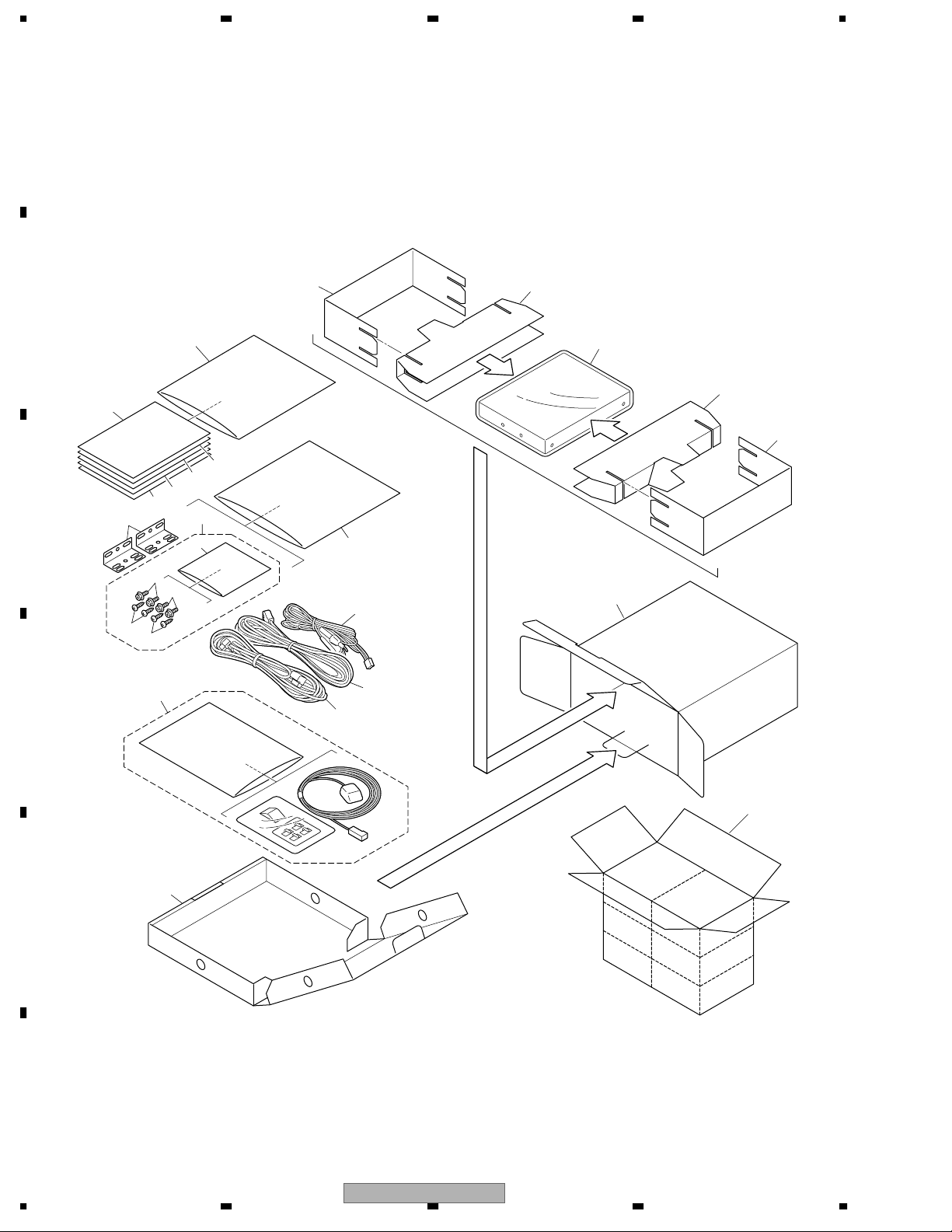
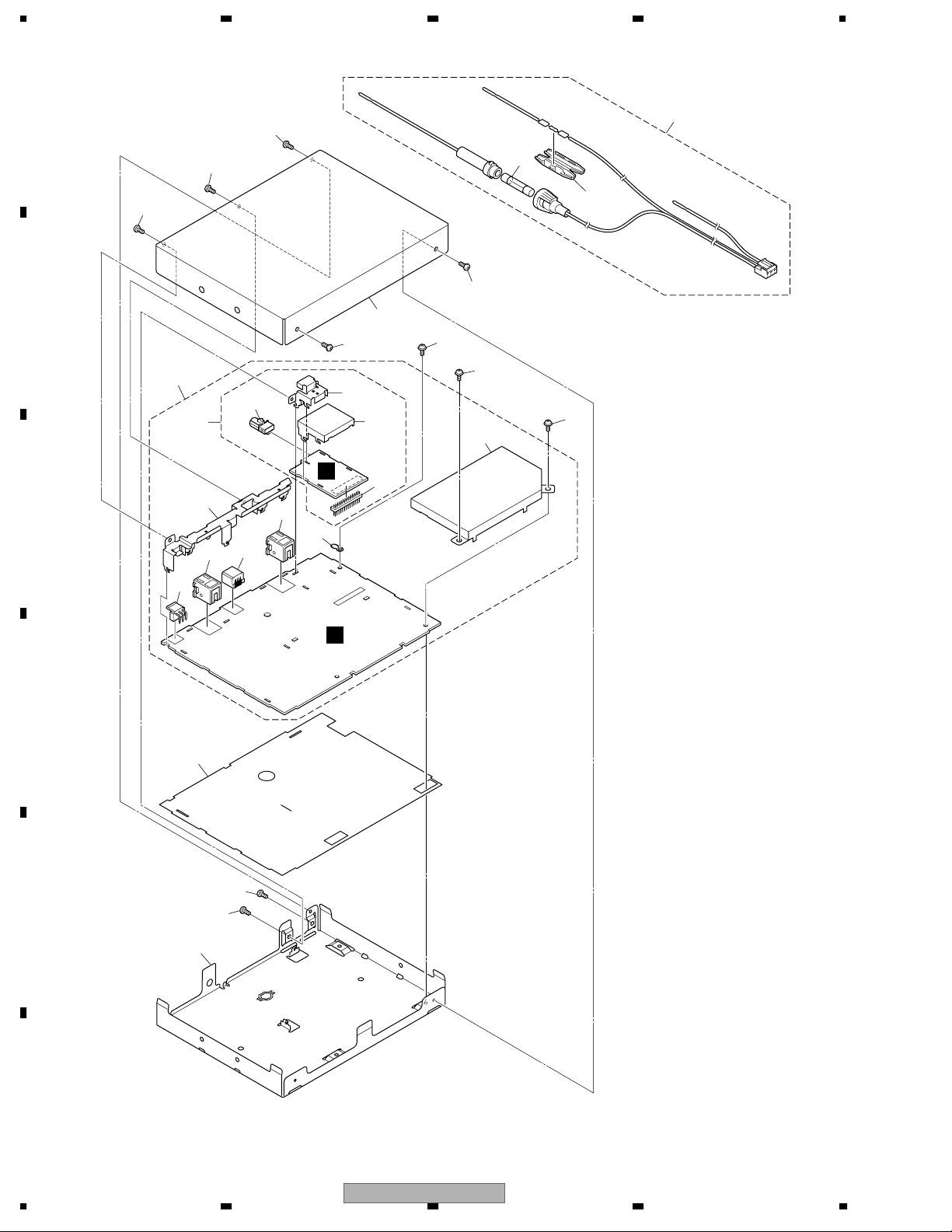
2. EXPLODED VIEWS AND PARTS LIST
OTES : • Parts marked by " * " are generally unavailable because they are not in our Master Spare Parts List.
• The > mark found on some component parts indicatesthe importance of the safety factor of the part.
A
Therefore, when replacing, be sure to use parts of identical designation.
• Screw adjacent to mark on the product are used for disassembly.
• For the applying amount of lobricants or glue, follow the instructions in this manual.
(In the case of no amount instructions,apply as you think it appropriate.)
2.1 PACKING
B
"
16 15
11
1
18
19
20
C
D
17
21
8
6
6
22
5
7
8
10
3
2
4
9
15
16
13
14
12
E
F
6
1234
GEX-P10XMT/XN/UC
Page 7

5678
PACKING SECTION PARTS LIST
Mark No. Description Part No.
* 1 Card ARY1048
2 Cord Assy CDE5880
3 Cord Assy CDE8009
4 Cord Assy CDE7836
5 Screw Assy CEA5014
6 Screw BNC40P120FTB
* 7 Polyethylene Bag CEG1158
8 Screw HMF40P060FTB
9 Cover CEG1098
* 10 Polyethylene Bag CEG1101
A
11 Polyethylene Bag CEG1116
12 Sub Carton CHG5471
13 Carton CHG5472
14 Contain Box CHL5472
15 Protector CHP2968
16 Protector CHP2969
17 Angle CNB2351
18 Owner's Manual(English) CRB2045
19 Installation Manual(English) CRB2046
* 20 Registration Card CRY1229
* 21 Caution Card CRN1079
22 Antenna Assy CXC4683
B
C
D
56
GEX-P10XMT/XN/UC
E
F
7
8
7
Page 8
1234
2.2 EXTERIOR
A
1
1
1
1
B
11
21
19
B
C
17
15
14
12
16
1
8
26
23
24
20
4
5
26
26
18
3
13
A
D
9
1
E
1
7
F
8
1234
GEX-P10XMT/XN/UC
Page 9

5678
EXTERIOR SECTION PARTS LIST
Mark No. Description Part No.
1 Screw BMZ26P030FTC
2 •••••
3 Cord Assy CDE8009
> 4 Fuse(2A) CEK1018
5 Cap CNS6329
6 •••••
7 Chassis CNA2807
8 Case CNB3106
9 Insulator CNM9419
10 •••••
A
11 Main Unit CWM9857
12 Terminal(CN603) CKF1064
13 Plug(CN901) CKS-460
14 Connector(CN402) CKS3409
15 Connector(CN401) CKS3410
16 Connector(CN451) CKS4473
17 Holder CND2697
18 Shield CND2744
19 Tuner Unit CWE1933
20 Connector(CN502) CKS5145
21 Connector(CN501) CKX1085
22 •••••
23 Shield CND2639
24 Holder CND2640
25 •••••
26 Screw ISS26P055FTC
B
C
D
56
GEX-P10XMT/XN/UC
E
F
7
8
9
Page 10
X
1234
3. BLOCK DIAGRAM AND SCHEMATIC DIAGRAM
3.1 BLOCK DIAGRAM
A
MAIN UNIT
A
B
B
TUNER UNIT
ZIF TUNER
IC501
MAX2140ETH
35
F501
CN501
XM SINGLE
ANTENNA
C
5
10
1
2
1
OUT1
IN
3
8
OUT2
16
5
6
F502
11
5
IN1
OUT1
10
6
OUT2
IN2
19
17
20
18
37
39
36
38
RFIN+
RFIN-
VOUTANT
IFOUT+
IFOUTIFIN-
IFIN+
IF2IO+
IF2IO-
IF2II+
IF2II-
IF2QO+
IF2QOIF2QI+
IF2QI-
QOUT-
QOUT+
IOUT-
IOUT+
AGCPWM
REFOUT
SDA
XTAL
SCL
34
21
22
9
25
44
43
VCC_ANT5.0V
24
4
IN-
MAX999EUK
VDD_M3.3V
VCC_RF3.3V
AMP
IC502
X501
IF_Q+
IF_Q-
IF_IIF_I+
IF_AGC
OUT
1
SYS_CLK
CN502
CN301
8
8
6
6
12
12
10
10
18
18
2
2
26
26
25
25
1
1
DIG_3.3V
15
15
17
RF_3.3V
ANT_5.0V
17
D
E
ST19AF08BR20QMAA
SDA
SDA
SCL
SCL
SDA
SCL
CAP
IC370
I2C_CLOCK
I2C_DATA
MCLK
RST
97
17
96
5
6
93
1
4
4
15
14
18
17
37
64
65
4
15
14
18
17
64
65
CAP_SDA_M
CAP_SCL_M
CAP_RST
CLKO
MCLK
INP1
INM1
MASTER
IC300
INM2
STA850P
INP2
AGC1
RAS,CAS,MDQM,MCSO
SDA
SCL
SM
108 107
Slave/master
108 107
SM
MCLK
INP1
INM1
INM2
INP2
SDA
SCL
NCSO,MWE,CLKON,MCKE
MADD0-11
MWE,CLKON,MCKE
RS232TX
CDEC_INTR
PCBS_SYNC
MFP_CLK
PCDC0
PCSD0
106100 99
983433
PCFS0
PCDC0
PCSD0
MFP_CLK
PCBS_SYNC
106
100 99 98
PCSD0
PCDC0
MFP_CLK
PCBS_SYNC
SLAVE
IC200
STA850P
MADD0-11
RAS,CAS,MDQM,
MDQ0-7
MBS0,1
MDQ0-7
MBS0,1
SD0
SCKT
LRCKT
OCLK
SRESET
PCFS0
RESET_N
34
33
PCFS0
SRESET
MRESET
84
83
82
81
D0-D7
A0-A11
BS0,BS1
RAS,CAS,DQM
CSO,WE,CLK,CKE
69
LSDPRX
66
INTR
CRESET
RESET_N
MRESET
CRESET
SD0-SD7
SA0-SA11
SBS0,SBS1
SRAS,SCAS,SDQM
SCSO,SWE,
SCLK,SCKE
D/A CONVERTER
IC480
PCM1742KE
2
DATA
VoutL
1
BCKIN VoutR
3
LRCKIN
16
MCLK
SDRAM
IC360
K4S280832F-TC75
DQ0-7
A0-11
BA0,1
RAS_,CAS_,
DQM,CS_,
WE_,CLK,CKE
VDD_3.3V
SDRAM
IC260
K4S280832F-TC75
DQ0-7
A0-11
BA0,1
RAS_,CAS_,
DQM,CS_,
WE_,CLK,CKE
2
7
IN-1
6
8
IN-2
15
DAC_EN
ML
14
DAC_CL
MC
DAC_DT
13
MD
RESET
IC603
S-80827CNNB-B8M
2
OUT
VDD
S602
RESET SW
LPF
IC490
NJM4558MD
1
OUT1
OUT2
SDA
SCL
1
7
X601
TEST
POINT
DAC_EN
DAC_CL
DAC_DT
RESET_N
MRESET
INTR
X602
LCH
RCH
11
13
30
18
10
TX
3
R
57
100
99
10
59
65
18
11
13
93
95
F
10
1234
GEX-P10XMT/XN/UC
Page 11
LPF
IC490
JM4558MD
-1
-2
EN
CL
DT
-B8M
1
T
SW
OUT1
OUT2
SDA
SCL
1
7
X601
TEST
POINT
DAC_EN
DAC_CL
DAC_DT
RESET_N
MRESET
INTR
X602
LCH
RCH
3
11
13
30
18
10
TX
RX
57
100
99
10
59
65
18
11
13
93
95
GND ISORATOR
1
8
AUDIO SELECTOR
3
18
19
2
SUB SYSTEM
CONTROL
Xout
IC605
PEG100A
Xin
LSDPRX
DATAINT
/RESET
2
1
DAC_EN
DACCL
DACDT
/RESET
RESET_N
MRESET
INTR
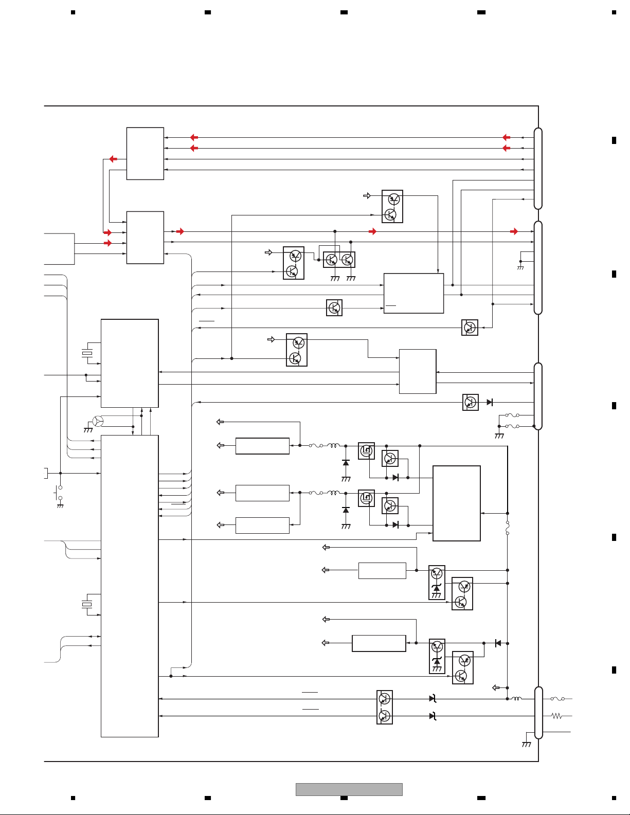
MAIN SYSTEM
CONTROL
IC601
PEG099A
Xout
Xin
SDA
SCL
5678
A
IC403
TA2050FS1
OUT1
OUT2
BA3131FS
+IN1B
+IN2B
-IN2A
-IN1A
MAINTX
33 34 17
33 36
34
SUBRX
IPOUT(TX)
IPIN(RX1)
ACCPW2
/BSENS
IC401
NAVIRX
NAVITX
MAINRX
SUBTX
ANSW
MUTE
IPPW
/ASENB
IPSW
XMPW
SYSPW
/ASENS
IN1B
IN1A
IN2A
IN2B
OUT2
OUT1
SW2
NC9
/SUBRES
27
28
43
72
82
49
37
73
71
42
28
27
20
40
15
13
12
10
14
7
9
ACCPW2
LCH
LCH
RCH
RCH
SEL
MUTE
IPIN
IPOUT
IPPW
ASENB
IPSW
SWITCH
5V
ACCPW2
LCH
RCH
SEL
MUTE
IPIN
IPOUT
IPPW
ASENB
ACCPW2
IPSW
DIG_3.3V
DIG_1.2V
RF_3.3V
ANT_5.0V
BUP
MUTE DRIVE
VDD_3.3V
1.2V REGULATOR
3
IC830
PQ012FZ01ZP
3.3V REGULATOR
3
IC842
BA033CC0FP
5V REGULATOR
4
IC841
NJM2880U1-05
1,2,4
1
1,5
Q404
Q403
SWITCH
Q452
FU854
FU855
AUDIO_8V
DAC_5V
VDD_3.3V
BSENS
ASENS
Q453
INV.
3.3V REGULATOR
6V REGULATOR
4
5V
4
Q451
MUTE
Q405
1
DIN1
2
DOUT
8
STBY
Q853
Q854
DAC5V
REGULATOR
IC802
NJM2880U1-05
VDD3.3V
REGULATOR
IC801
S-T111B33MC-OGS
BACKUP SENSE
Q911
IP-BUS DRIVER
IC451
HA12240FP
RS232C DRIVER
IC452
UPD4721GS
1
VDD
10
Rout2
8
Din2
Q851
Q852
1,5
SYSPW
1,5
ACCPW2
BSENS
ASENS
7
VCC
6
BUS+
5
BUS-
Q402
11
Rin2
13
Dout2
DC/DC CONVERTER
7
10
3
Q811
VDD5V REGULATOR
Q801
3.3V/6V DUAL
OUT2
IC851
AN8011S
OUT1
ON/OFF
AUDIO8V
REGULATOR
Q812
Q802
Q454
VCC
9
BUP
ACC SENSE
FU451
FU452
FU851
CN401
CN402
CN451
CN901
BUP
ACC
11
7
9
10
1
5
8
7
9
11
10
1
5
8
7
8
10
3
3
2
1
DATA OUT IP-BUS OUT IP-BUS IN
BACKUP
ACC
GND
B
C
D
E
F
56
GEX-P10XMT/XN/UC
7
8
11
Page 12
1234
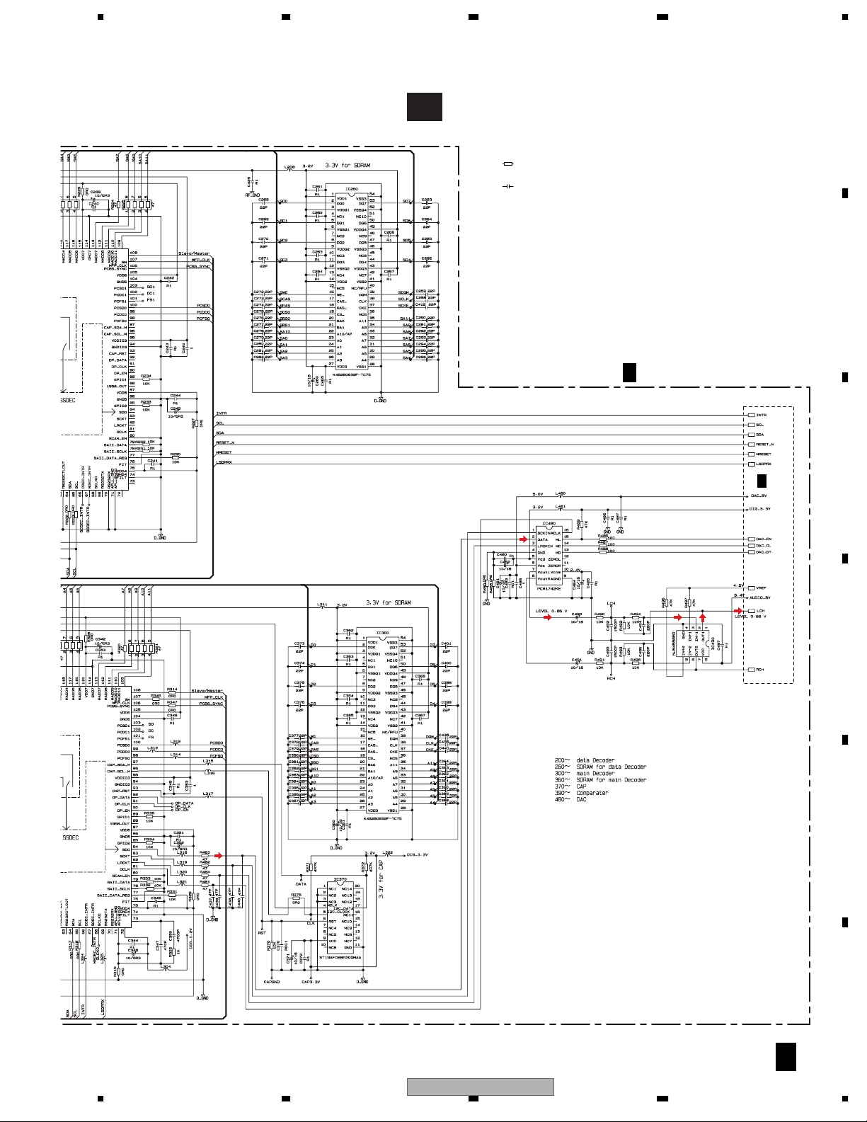
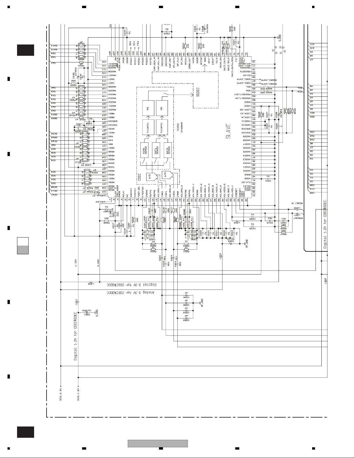
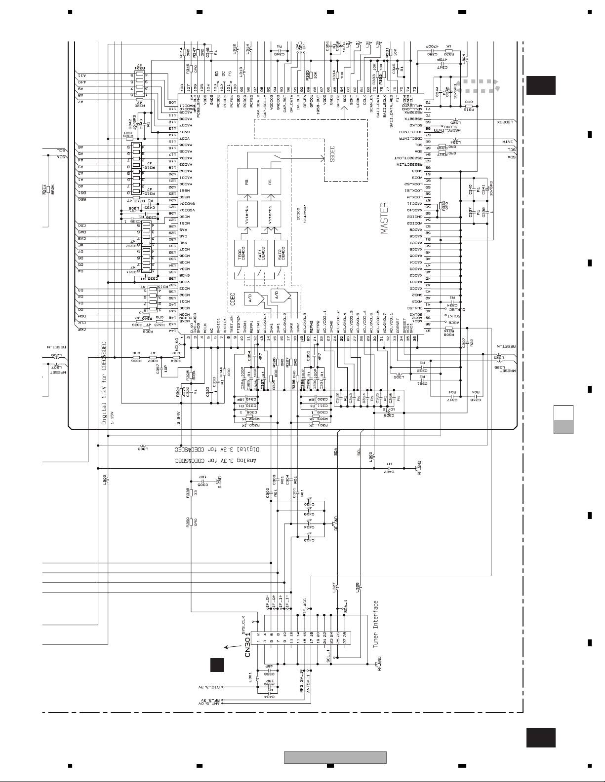
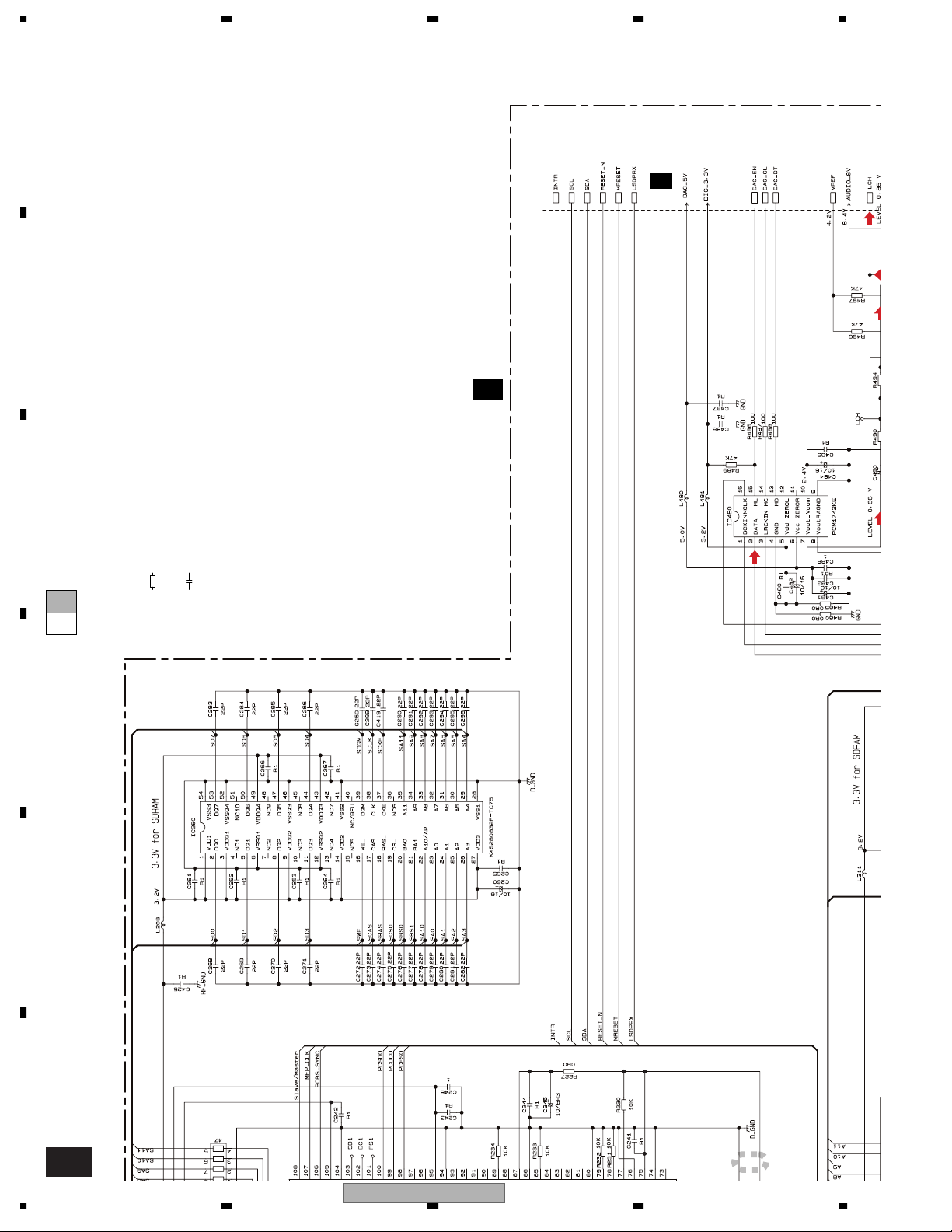
3.2 MAIN UNIT(DSP)
Note: When ordering service parts, be sure to refer to " EXPLODED VIEWS AND PARTS LIST" or
"ELECTRICAL PARTS LIST".
A
Large size
A-b
SCH diagram
Guide page
A-a A-b
A-a
A-a
1/2
A-b
Detailed page
A-a
B
C
D
CN502
B
E
F
12
A
1/2
GEX-P10XMT/XN/UC
1234
Page 13
5678
A-b
1/2
NOTE :
Symbol indicates a resistor.
No differentiation is made between chip resistors and
discrete resistors.
Symbol indicates a capacitor.
No differentiation is made between chip capacitors and
discrete capacitors.
The > mark found on some component parts indicates
the importance of the safety factor of the part.
Therefore, when replacing, be sure to use parts of
identical designation.
A
MAIN UNIT(DSP)
1/2
Decimal points for resistor
and capacitor fixed values
are expressed as :
←
2.2 2R2
←
0.022 R022
A
A
B
C
2/2
DAC
D
LPF
E
56
GEX-P10XMT/XN/UC
F
1/2
A
7
8
13
Page 14
A
B
A-b
1234
1/2
1
C
A-b
A-a
A-a
D
E
F
A-a
14
1/2
GEX-P10XMT/XN/UC
1234
Page 15
5678
A
2
A-b
1/2
B
A-b
A-a
A-a
C
D
E
CN502
B
GEX-P10XMT/XN/UC
56
F
A-a
1/2
7
8
15
Page 16
1234
A
2/2
A
←
←
Decimal points for resistor
and capacitor fixed values
are expressed as :
2.2 2R2
0.022 R022
B
MAIN UNIT(DSP)
1/2
A
C
The > mark found on some component parts indicates
the importance of the safety factor of the part.
Therefore, when replacing, be sure to use parts of
Symbol indicates a resistor.
No differentiation is made between chip resistors and
discrete resistors.
Symbol indicates a capacitor.
No differentiation is made between chip capacitors and
discrete capacitors.
A-b
A-a
D
E
NOTE :
identical designation.
DAC
F
A-b
16
1/2
1
GEX-P10XMT/XN/UC
1234
Page 17
5678
A
LPF
B
C
A-b
A-a
D
56
GEX-P10XMT/XN/UC
E
F
2
7
A-b
8
1/2
17
Page 18
1234
D
R
3.3 MAIN UNIT(SYSCOM)
A
A-a
2/2
3.3V/6V
DC/DC C
DIGITAL 1.2V REGULATOR
B
1/2
A
C
RF 3.3V REGULATOR
ANT 5V REGULATOR
>
>
D
DATA MICROCOMPUTER
E
F
: The power supply is shown with the marked box.
SYSTEM MICROCOMPUTER
18
A
2/2
GEX-P10XMT/XN/UC
1234
Page 19
5678
A-b
2/2
MAIN UNIT(SYSCOM)
2/2
A
A
3.3V/6V DUAL
DC/DC CONVERTER
>
AUDIO SELECTOR
DAC 5V
REGULATOR
VDD 3.3V REGULATOR
AUDIO 8V REGULATOR
BACKUP
SENSE
ACC SENSE
5V REGULATOR
>
2A
BACKUP
ACC
GND
B
C
ROCOMPUTER
RESET
IP-BUS DRIVER
DATA COMMUNICATION
IP-BUS IN
IP-BUS OUT
>
DATA OUT
>
D
E
F
56
GEX-P10XMT/XN/UC
2/2
A
7
8
19
Page 20
A
A-b
1234
3.3V/6DC/D
2/2
2 431
>
B
C
DIGITAL 1.2V REGULATOR
>
A-b
A-a
A-a
D
E
RF 3.3V REGULATOR
ANT 5V REGULATOR
1/2
F
A
A-a
20
2/2
GEX-P10XMT/XN/UC
1234
Page 21

R
5678
5
SYSTEM MICROCOMPUTE
A-b
2/2
A
B
C
DATA MICROCOMPUTER
A-b
A-a
A-a
D
E
: The power supply is shown with the marked box.
56
GEX-P10XMT/XN/UC
F
A-a
2/2
7
8
21
Page 22

1234
A
B
MAIN UNIT(SYSCOM)
>
2A
BACKUP
GND
ACC
BACKUP
SENSE
N
2/2
A
AUDIO 8V REGULATOR
C
ACC SENSE
5V REGULATOR
A-b
A-a
DAC 5V
REGULATOR
D
>
E
VDD 3.3V REGULATOR
AUDIO SELECTOR
F
A-b
22
3.3V/6V DUAL
DC/DC CONVERTER
2/2
1234
2 431
GEX-P10XMT/XN/UC
Page 23

5678
A
IP-BUS IN
IP-BUS OUT
DATA OUT
>
>
B
C
A-b
A-a
DATA COMMUNICATION
IP-BUS DRIVER
RESET
OCOMPUTER
GEX-P10XMT/XN/UC
56
D
E
F
5
7
A-b
8
2/2
23
Page 24

1234
3.4 TUNER UNIT
A
B
RF
C
D
E
XM
ANTENNA
F
B
24
1234
GEX-P10XMT/XN/UC
Page 25

5678
A
TUNER UNIT
B
B
CLK BUFFER
A
1/2
CN301
C
D
E
56
GEX-P10XMT/XN/UC
F
B
7
8
25
Page 26

1234
4. PCB CONNECTION DIAGRAM
4.1 MAIN UNIT
A
B
C
NOTE FOR PCB DIAGRAMS
1.The parts mounted on this PCB
include all necessary parts for
several destination.
For further information for
respective destinations, be sure
to check with the schematic dia gram.
2.Viewpoint of PCB diagrams
Connector
P.C.Board
Capacitor
Chip Part
SIDE A
SIDE B
MAIN UNIT
A
130
120
110
100
90
80
70
60
D
50
CN502
B
40
E
30
20
10
IP-BUS OUT
F
Y
0
10 20 30 40 50 60 70
X
A
26
1234
GEX-P10XMT/XN/UC
Page 27

5678
SIDE A
A
B
C
70 80
DATA OUT
IP-BUS IN
RESET
90 100 110 120 130 140 150
FRONT
56
GEX-P10XMT/XN/UC
D
E
CORD ASSY
F
160 170
A
7
8
27
Page 28

1234
A
MAIN UNIT
A
B
C
D
E
F
160170
90100110120130140150
A
28
1234
GEX-P10XMT/XN/UC
Page 29

5678
130
120
110
100
90
80
SIDE B
A
B
C
70
60
D
50
40
30
20
10
E
Y
90
1020304050607080
0
X
F
A
56
GEX-P10XMT/XN/UC
7
8
29
Page 30

1234
4.2 TUNER UNIT
A
TUNER UNIT
B
B
A
30
C
20
XM ANTENNA
10
D
SIDE A
CN301
Y
0
X
E
F
10
20
30
40
50
B
30
1234
GEX-P10XMT/XN/UC
Page 31

5678
A
TUNER UNIT
B
SIDE B
30
20
10
B
C
D
50
56
40
30
GEX-P10XMT/XN/UC
20
Y
10
X
0
E
F
B
7
8
31
Page 32

1234
5. ELECTRICAL PARTS LIST
NOTE:
A
• Parts whose parts numbers are omitted are subject to being not supplied.
• The part numbers shown below indicate chip components.
Chip Resistor
RS1/_S___J,RS1/__S___J
Chip Capacitor (except for CQS.....)
CKS....., CCS....., CSZS.....
• The > mark found on some component parts indicatesthe importance of the safety factor of the part.
Therefore, when replacing, be sure to use parts of identical designation.
• Meaning of the figures and others in the parentheses in the parts list.
B
Example) IC 301 is on the point (face A, 91 of x-axis, and 111 of y-axis) of the corresponding
PC board.
IC 301 (A, 91, 111) IC NJM2068V
Circuit Symbol and No. Part No.
A
Unit Number:CWM9857
Unit Name:Main Unit
C
MISCELLANEOUS
IC 200 (A,34,92) IC STA850P
IC 260 (A,34,122) IC K4S280832F-TC75
IC 300 (A,82,92) IC STA850P
IC 360 (A,82,122) IC K4S280832F-TC75
IC 370 (A,55,118) IC ST19AF08BR20QMAA
IC 401 (A,123,31) IC BA3131FS
IC 403 (A,142,28) IC T A2050FS1
IC 451 (A,64,19) IC HA12240FP
IC 452 (A,88,17) IC UPD4721GS
D
IC 480 (A,118,79) IC PCM1742KE
IC 490 (A,123,59) IC NJM4558MD
IC 601 (A,66,51) IC PEG099A
IC 603 (A,51,41) IC S-80827CNNB-B8M
IC 605 (A,99,43) IC PEG100A
IC 801 (A,141,67) IC S-T111B33MC-OGS
IC 802 (A,142,43) IC NJM2880U1-05
IC 830 (A,113,105) IC PQ012FZ01ZP
IC 841 (A,137,111) IC NJM2880U1-05
IC 842 (A,150,120) IC BA033CC0FP
E
IC 851 (A,142,100) IC AN8011S
Q 402 (A,52,36) Transistor 2SC4081
Q 403 (A,55,30) Transistor DTC144EU
Q 404 (A,60,27) Transistor 2SA1162
Q 405 (A,56,26) Transistor UMH3N
Q 451 (A,69,22) Transistor UMD2N
Q 452 (A,77,26) Transistor UMD2N
Q 453 (A,69,15) Transistor DTC144EU
Q 454 (A,86,6) Transistor 2SC4081
Q 801 (A,145,58) Transistor 2SD1760F5
Q 802 (A,148,67) Transistor UMD2N
F
Q 811 (A,156,43) Transistor 2SD1767
Q 812 (A,156,47) Transistor UMD2N
Q 851 (A,118,90) Transistor 2SC4081
Circuit Symbol and No. Part No.
Q 852 (A,152,89) Transistor 2SC4081
Q 853 (A,127,90) Transistor 2SJ529S
Q 854 (A,161,90) Transistor 2SJ529S
Q 911 (A,149,35) Transistor IMX1
D 451 (A,96,16) Diode UDZS12(B)
D 452 (A,96,18) Diode UDZS12(B)
D 453 (A,102,22) Diode UDZS12(B)
D 454 (A,102,20) Diode UDZS12(B)
D 455 (A,92,7) Diode 1SS355
D 456 (A,66,10) Diode DAN202U
D 457 (A,147,12) Diode UMZ6R8N
D 458 (A,147,15) Diode UMZ6R8N
D 459 (A,143,12) Diode UMZ6R8N
D 460 (A,143,15) Diode UMZ6R8N
D 801 (A,163,65) Diode 1SR154-400
D 802 (A,151,54) Diode UDZS5R6(B)
D 811 (A,154,48) Diode UDZS9R1(B)
D 851 (A,168,65) Diode RB051L-40
D 853 (A,118,94) Diode 1SS355
D 854 (A,151,94) Diode 1SS355
D 855 (A,135,89) Diode RSX201L-30
D 856 (A,161,84) Diode RSX201L-30
D 901 (A,156,36) Diode 1SR154-400
D 911 (A,155,30) Diode UDZS7R5(B)
D 912 (A,155,26) Diode UDZS6R8(B)
L 201 (A,49,104) Inductor CTF1306
L 202 (A,51,104) Inductor CTF1306
L 203 (A,16,80) Inductor CTF1306
L 204 (A,19,81) Inductor CTF1306
L 205 (A,33,104) Ferrite Bead CTF1528
L 207 (A,23,77) Ferrite Bead CTF1528
L 208 (A,19,115) Inductor CTF1306
L 209 (A,26,77) Ferrite Bead CTF1528
L 301 (A,8,65) Inductor LCYB27NJ1005
L 302 (A,98,110) Inductor CTF1306
L 303 (A,99,107) Inductor CTF1306
L 304 (A,95,77) Inductor CTF1473
L 305 (A,65,80) Inductor CTF1306
L 306 (A,67,80) Inductor CTF1306
L 309 (A,82,104) Ferrite Bead CTF1528
L 311 (A,67,117) Inductor CTF1306
32
1234
GEX-P10XMT/XN/UC
Page 33

5678
Circuit Symbol and No. Part No.
L 312 (A,99,98) Ferrite Bead CTF1528
Circuit Symbol and No. Part No.
R 219 (A,35,109) RAB4CQ470J
>
>
>
>
>
L 313 (A,97,97) Ferrite Bead CTF1528
L 314 (A,97,96) Ferrite Bead CTF1528
L 315 (A,97,95) Ferrite Bead CTF1528
L 316 (A,97,94) Ferrite Bead CTF1528
L 317 (A,62,115) Ferrite Bead CTF1528
L 318 (A,97,88) Chip Bead VTL1128
L 319 (A,97,87) Chip Bead VTL1128
L 320 (A,97,86) Chip Bead VTL1128
L 321 (A,97,85) Chip Bead VTL1128
L 322 (A,62,126) Inductor CTF1306
L 323 (A,77,75) Ferrite Bead CTF1528
L 324 (A,89,78) Ferrite Bead CTF1528
L 325 (A,90,77) Ferrite Bead CTF1528
L 326 (A,77,74) Ferrite Bead CTF1528
L 327 (A,41,66) Inductor CTF1306
L 328 (A,44,66) Inductor CTF1306
L 451 (A,68,19) Inductor CTF1473
L 452 (A,80,20) Inductor CTF1473
L 453 (A,96,19) Inductor CTF1334
L 454 (A,96,21) Inductor CTF1334
L 480 (A,121,73) Inductor CTF1473
L 481 (A,120,73) Inductor CTF1473
L 602 (A,69,39) Inductor CTF1473
L 603 (A,95,56) Inductor CTF1473
L 851 (A,152,76) Inductor CTH1253
R 220 (A,45,77) RS1/16S822J
R 221 (A,38,109) RAB4CQ470J
R 222 (A,42,77) RS1/16S0R0J
R 223 (A,44,77) RS1/16S0R0J
R 224 (A,44,106) RS1/16SS470J
R 225 (A,46,105) RAB4CQ470J
R 227 (A,50,89) RS1/16S0R0J
R 228 (A,29,77) RS1/16S0R0J
R 229 (A,42,109) RS1/16S0R0J
R 230 (A,47,84) RS1/16SS103J
R 231 (A,47,85) RS1/16SS103J
R 232 (A,47,86) RS1/16SS103J
R 233 (A,47,88) RS1/16SS103J
R 234 (A,47,92) RS1/16SS103J
R 300 (A,61,98) RS1/16SS102J
R 301 (A,60,88) RS1/16SS102J
R 302 (A,61,97) RS1/16SS102J
R 303 (A,61,88) RS1/16SS102J
R 304 (A,64,101) RS1/16SS4701F
R 305 (A,65,102) RS1/16SS3301F
R 306 (A,64,104) RS1/16SS0R0J
R 307 (A,67,103) RS1/16SS470J
R 308 (A,73,78) RS1/16SS512J
R 309 (A,71,105) RS1/16SS470J
R 310 (A,74,107) RAB4CQ470J
A
B
C
L 852 (A,146,90) Inductor LCY A100J2520
L 853 (A,123,102) Inductor CTH1262
L 854 (A,161,101) Inductor CTH1262
L 901
X 601 (A,100,60) Resonator 16.77Hz CSS1686
X 602 (A,62,36) Resonator 10.00Hz CSS1685
S 602 (A,117,7) Switch(RESET) CSG1046
FU451 (A,106,18) Fuse 2A CEK1284
FU452 (A,108,16) Fuse 2A CEK1284
FU851 (A,162,69) Fuse 2A CEK1284
FU854 (A,120,110) Fuse 2A CEK1284
FU855 (A,155,107) Fuse 1A CEK1280
(A,166,36) Choke Coil 1.4mH CTH1129
RESISTORS
R 200 (A,15,98) RS1/16SS102J
R 201 (A,13,88) RS1/16SS102J
R 202 (A,15,97) RS1/16SS102J
R 203 (A,14,88) RS1/16SS102J
R 204 (A,21,78) RS1/16SS223J
R 205 (A,24,78) RS1/16SS223J
R 206 (A,20,102) RS1/16SS3002F
R 207 (A,19,101) RS1/16SS2002F
R 208 (A,18,98) RS1/16S0R0J
R 209 (A,25,107) RAB4CQ470J
R 210 (A,28,107) RAB4CQ470J
R 211 (A,30,108) RAB4CQ470J
R 212 (A,35,105) RS1/16SS470J
R 213 (A,22,107) RS1/16SS0R0J
R 214 (A,41,77) RS1/16S822J
R 215 (A,18,93) RS1/16SS0R0J
R 216 (A,20,93) RS1/16SS0R0J
R 217 (A,18,92) RS1/16SS0R0J
R 218 (A,20,91) RS1/16SS0R0J
56
R 311 (A,76,107) RAB4CQ470J
R 312 (A,79,107) RAB4CQ470J
R 313 (A,84,105) RS1/16SS470J
R 314 (A,97,102) RS1/16S0R0J
R 315 (A,84,109) RAB4CQ470J
R 316 (A,87,109) RAB4CQ470J
R 317 (A,87,78) RS1/16S0R0J
R 318 (A,88,78) RS1/16S0R0J
R 319 (A,99,78) RS1/16SS0R0J
R 320 (A,93,106) RS1/16SS470J
R 321 (A,95,106) RAB4CQ470J
R 322 (A,97,78) RS1/16SS102J
R 323 (A,71,106) RS1/16SS0R0J
R 324 (A,70,102) RS1/16SS0R0J
R 325 (A,65,93) RS1/16SS0R0J
R 326 (A,67,93) RS1/16SS0R0J
R 327 (A,67,92) RS1/16SS0R0J
R 328 (A,90,109) RS1/16S0R0J
R 329 (A,99,92) RS1/16S0R0J
R 330 (A,80,76) RS1/16S0R0J
R 331 (A,97,81) RS1/16SS103J
R 332 (A,97,83) RS1/16SS103J
R 333 (A,97,84) RS1/16SS103J
R 334 (A,97,89) RS1/16SS103J
R 335 (A,95,91) RS1/16SS103J
R 336 (A,65,91) RS1/16SS0R0J
R 338 (A,61,101) RS1/16SS330J
R 339 (A,71,107) RS1/16SS470J
R 340 (A,71,108) RS1/16SS470J
R 341 (A,22,106) RS1/16SS470J
R 342 (A,22,108) RS1/16SS470J
R 343 (A,22,109) RS1/16SS470J
R 344 (A,68,97) RS1/16S0R0J
R 346 (A,97,101) RS1/16S0R0J
GEX-P10XMT/XN/UC
D
E
F
7
8
33
Page 34

1234
Circuit Symbol and No. Part No.
R 347 (A,97,99) RS1/16S0R0J
Circuit Symbol and No. Part No.
R 491 (A,115,60) RS1/16S103J
R 370 (A,62,117) RS1/16SS103J
A
R 371 (A,62,122) RS1/16S472J
R 372 (A,63,122) RS1/16S472J
R 375 (A,62,114) RS1/16S0R0J
R 390 (A,58,101) RS1/16SS0R0J
R 401 (A,118,41) RS1/16S103J
R 402 (A,118,25) RS1/16S103J
R 403 (A,118,38) RS1/16S473J
R 404 (A,119,25) RS1/16S473J
R 405 (A,125,38) RS1/16S103J
R 406 (A,126,25) RS1/16S103J
R 407 (A,120,38) RS1/16S473J
B
R 408 (A,121,25) RS1/16S473J
R 409 (A,123,38) RS1/16S562J
R 410 (A,124,25) RS1/16S562J
R 411 (A,122,38) RS1/16S473J
R 412 (A,123,25) RS1/16S473J
R 413 (A,127,25) RS1/16S473J
R 415 (A,50,36) RS1/16S473J
R 416 (A,48,36) RS1/16S102J
R 417 (A,129,36) RS1/16S473J
R 418 (A,130,25) RS1/16S473J
R 419 (A,61,30) RS1/16S103J
C
R 420 (A,58,30) RS1/16S333J
R 421 (A,65,13) RS1/16S101J
R 492 (A,131,56) RS1/16S103J
R 493 (A,115,56) RS1/16S103J
R 494 (A,131,58) RS1/16S103J
R 495 (A,115,58) RS1/16S103J
R 496 (A,118,61) RS1/16S473J
R 497 (A,128,61) RS1/16S473J
R 601 (A,86,41) RS1/16S473J
R 602 (A,87,39) RS1/16S473J
R 603 (A,68,32) RS1/16S473J
R 604 (A,62,40) RS1/16S0R0J
R 605 (A,105,53) RS1/16S473J
R 606 (A,101,32) RS1/16S473J
R 608 (A,113,28) RS1/16S104J
R 610 (A,78,42) RS1/16S473J
R 611 (A,78,45) RS1/16S473J
R 612 (A,81,56) RS1/16S473J
R 613 (A,79,53) RS1/16S473J
R 614 (A,79,56) RS1/16S473J
R 615 (A,81,62) RS1/16S473J
R 617 (A,51,44) RS1/16S183J
R 618 (A,54,44) RS1/16S102J
R 619 (A,62,64) RS1/16S473J
R 620 (A,60,64) RS1/16S473J
R 621 (A,59,64) RS1/16S473J
R 622 (A,55,38) RS1/16S473J
R 422 (A,64,13) RS1/16S101J
R 423 (A,51,23) RS1/16S102J
R 424 (A,60,23) RS1/16S102J
R 425 (A,148,21) RS1/16S102J
R 426 (A,142,18) RS1/16S102J
R 427 (A,57,23) RS1/16S223J
R 428 (A,56,23) RS1/16S223J
R 429 (A,148,18) RS1/16S223J
R 430 (A,143,18) RS1/16S223J
D
R 431 (A,146,18) RS1/16S181J
R 432 (A,145,18) RS1/16S181J
R 433 (A,71,31) RS1/16S473J
R 451 (A,70,19) RS1/16S103J
R 453 (A,81,15) RS1/16S101J
R 454 (A,96,23) RS1/16S101J
R 455 (A,101,19) RS1/16S681J
R 456 (A,102,17) RS1/16S681J
R 457 (A,86,23) RS1/16S101J
R 458 (A,88,23) RS1/16S101J
R 459 (A,87,10) RS1/16S333J
E
R 460 (A,90,8) RS1/16S333J
R 461 (A,90,7) RS1/16S333J
R 462 (A,90,5) RS1/16S333J
R 480 (A,110,68) RS1/16S0R0J
R 481 (A,102,82) RS1/16S470J
R 623 (A,63,64) RS1/16S473J
R 625 (A,49,62) RS1/16S104J
R 629 (A,92,56) RS1/16S473J
R 630 (A,101,55) RS1/16S0R0J
R 631 (A,81,49) RS1/16S101J
R 632 (A,78,50) RS1/16S101J
R 633 (A,53,45) RS1/16S101J
R 634 (A,53,47) RS1/16S101J
R 635 (A,53,53) RS1/16S101J
R 636 (A,81,55) RS1/16S101J
R 637 (A,53,55) RS1/16S101J
R 638 (A,65,64) RS1/16S101J
R 639 (A,69,64) RS1/16S101J
R 640 (A,70,64) RS1/16S101J
R 641 (A,78,61) RS1/16S101J
R 642 (A,78,59) RS1/16S101J
R 643 (A,82,59) RS1/16S101J
R 644 (A,78,52) RS1/16S101J
R 645 (A,81,51) RS1/16S101J
R 646 (A,78,44) RS1/16S101J
R 647 (A,78,47) RS1/16S101J
R 649 (A,74,31) RS1/16S101J
R 650 (A,82,46) RS1/16S101J
R 651 (A,88,52) RS1/16S101J
R 652 (A,87,49) RS1/16S101J
R 482 (A,99,87) RS1/16SS470J
R 483 (A,99,88) RS1/16SS470J
R 484 (A,102,86) RS1/16S470J
R 485 (A,116,66) RS1/16S0R0J
R 486 (A,111,83) RS1/16S101J
F
R 487 (A,111,84) RS1/16S101J
R 488 (A,111,86) RS1/16S101J
R 489 (A,111,87) RS1/16S473J
R 490 (A,131,61) RS1/16S103J
34
1234
R 653 (A,87,48) RS1/16S101J
R 656 (A,81,48) RS1/16S473J
R 657 (A,53,52) RS1/16S101J
R 658 (A,87,45) RS1/16S101J
R 659 (A,86,42) RS1/16S101J
R 665 (A,89,55) RS1/16S101J
R 666 (A,82,28) RS1/16S473J
R 669 (A,99,55) RS1/16S105J
R 801 (A,150,59) RS1/16S272J
GEX-P10XMT/XN/UC
Page 35

5678
Circuit Symbol and No. Part No.
R 802 (A,150,58) RS1/16S223J
R 804 (A,155,56) RS1/16S360J
R 805 (A,155,54) RS1/16S360J
R 811 (A,159,44) RS1/16S182J
R 847 (A,7,59) RS1/16S0R0J
R 848 (A,8,53) RS1/16S0R0J
R 851 (A,133,101) RS1/16S2701D
R 852 (A,133,100) RS1/16S0R0J
R 853 (A,132,98) RS1/16S1801D
R 854 (A,132,97) RS1/16S8200D
R 855 (A,137,100) RS1/16S1203D
R 856 (A,136,102) RS1/16S2701D
R 857 (A,136,93) RS1/16S221J
R 859 (A,135,106) RS1/16S6801D
R 860 (A,137,106) RS1/16S6801D
R 861 (A,136,98) RS1/16S0R0J
R 862 (A,148,94) RS1/16S221J
R 863 (A,151,98) RS1/16S3901D
R 864 (A,151,101) RS1/16S3302D
R 865 (A,151,100) RS1/16S0R0J
R 866 (A,149,97) RS1/16S2002D
R 867 (A,147,100) RS1/16S2203D
R 868 (A,148,102) RS1/16S2701D
R 869 (A,151,97) RS1/16S4701D
R 870 (A,148,105) RS1/16S1502D
R 871 (A,151,105) RS1/16S6801D
R 872 (A,149,105) RS1/16S0R0J
R 873 (A,117,92) RS1/16S272J
R 874 (A,121,94) RS1/16S0R0J
R 875 (A,152,92) RS1/16S272J
R 876 (A,155,94) RS1/16S0R0J
R 879 (A,160,79) RS1/16S360J
R 880 (A,160,81) RS1/16S360J
R 881 (A,145,71) RS1/16S360J
R 882 (A,145,73) RS1/16S360J
R 913 (A,152,32) RS1/16S103J
R 914 (A,152,30) RS1/16S473J
R 915 (A,155,28) RS1/16S472J
R 916 (A,152,26) RS1/16S103J
R 917 (A,152,27) RS1/16S473J
CAPACITORS
C 200 (A,12,93) CKSSYB103K16
C 201 (A,13,90) CKSSYB103K16
C 202 (A,12,92) CKSSYB103K16
C 203 (A,12,91) CKSSYB103K16
C 204 (A,12,79) CEVW100M16
C 205 (A,13,95) CKSRYB105K6R3
C 206 (A,15,85) CKSRYB105K6R3
C 207 (A,16,94) CKSSYB104K10
C 208 (A,17,85) CKSSYB104K10
C 209 (A,16,90) CKSSYB104K10
C 210 (A,18,86) CKSSYB104K10
C 211 (A,18,85) CKSSYB104K10
C 212 (A,18,84) CKSSYB104K10
C 213 (A,18,83) CKSSYB104K10
C 214 (A,15,95) CCSRCH180J50
C 215 (A,14,85) CCSRCH180J50
C 216 (A,21,82) CKSSYB104K10
56
Circuit Symbol and No. Part No.
C 217 (A,18,103) CKSSYB104K10
C 218 (A,18,100) CKSRYB105K6R3
C 219 (A,22,78) CKSSYB103K16
C 220 (A,23,78) CKSSYB103K16
C 221 (A,18,94) CCSSCH101J50
C 222 (A,17,94) CKSSYB104K10
C 223 (A,19,94) CCSSCH101J50
C 224 (A,20,94) CKSSYB104K10
C 225 (A,20,90) CCSSCH101J50
C 226 (A,19,90) CKSSYB104K10
C 227 (A,17,90) CCSSCH101J50
C 228 (A,18,90) CKSSYB104K10
C 229 (A,21,84) CKSSYB104K10
C 230 (A,18,101) CKSSYB104K10
C 231 (A,28,79) CKSSYB104K10
C 232 (A,28,105) CKSSYB104K10
C 233 (A,32,107) CKSRYB105K6R3
C 234 (A,33,79) CKSSYB104K10
C 235 (A,33,77) CKSRYB105K6R3
C 236 (A,34,106) CKSSYB104K10
C 237 (A,36,79) CKSSYB104K10
C 238 (A,37,77) CSZS100M6R3
C 239 (A,41,106) CSZS100M6R3
C 240 (A,40,105) CKSSYB104K10
C 241 (A,47,82) CKSSYB104K10
C 242 (A,47,99) CKSSYB104K10
C 243 (A,47,94) CKSSYB104K10
C 244 (A,47,90) CKSSYB104K10
C 245 (A,49,89) CSZS100M6R3
C 246 (A,48,94) CKSRYB105K6R3
C 247 (A,18,96) CKSQYB475K6R3
C 248 (A,17,88) CKSQYB475K6R3
C 251 (A,51,106) CSZS100M6R3
C 252 (A,16,103) CCSSCH100D50
C 253 (A,10,88) CCSSCH4R0C50
C 254 (A,10,90) CCSSCH4R0C50
C 255 (A,10,92) CCSSCH4R0C50
C 256 (A,10,93) CCSSCH4R0C50
C 257 (A,21,103) CKSSYB104K10
C 258 (A,34,105) CKSSYB104K10
C 259 (A,36,130) CCSSCH220J50
C 260 (A,20,120) CEVW100M16
C 261 (A,24,114) CKSSYB104K10
C 262 (A,26,114) CKSSYB104K10
C 263 (A,30,114) CKSSYB104K10
C 264 (A,33,114) CKSSYB104K10
C 265 (A,46,114) CKSSYB104K10
C 266 (A,28,130) CKSSYB104K10
C 267 (A,33,130) CKSSYB104K10
C 268 (A,23,114) CCSSCH220J50
C 269 (A,27,114) CCSSCH220J50
C 270 (A,29,114) CCSSCH220J50
C 271 (A,32,114) CCSSCH220J50
C 272 (A,35,114) CCSSCH220J50
C 273 (A,36,114) CCSSCH220J50
C 274 (A,37,114) CCSSCH220J50
C 275 (A,38,114) CCSSCH220J50
C 276 (A,39,114) CCSSCH220J50
C 277 (A,40,114) CCSSCH220J50
C 278 (A,41,114) CCSSCH220J50
GEX-P10XMT/XN/UC
A
B
C
D
E
F
7
8
35
Page 36

1234
Circuit Symbol and No. Part No.
C 279 (A,42,114) CCSSCH220J50
C 280 (A,43,114) CCSSCH220J50
C 281 (A,44,114) CCSSCH220J50
A
C 282 (A,45,114) CCSSCH220J50
C 283 (A,25,130) CCSSCH220J50
C 284 (A,27,130) CCSSCH220J50
C 285 (A,29,130) CCSSCH220J50
C 286 (A,31,130) CCSSCH220J50
Circuit Symbol and No. Part No.
C 345 (A,93,77) CSZS100M6R3
C 346 (A,96,81) CKSSYB104K10
C 347 (A,96,78) CKSSYB471K50
C 348 (A,95,98) CKSSYB104K10
C 349 (A,95,93) CKSSYB104K10
C 350 (A,97,79) CKSRYB472K50
C 351 (A,97,90) CKSSYB104K10
C 352 (A,100,90) CSZS100M6R3
C 290 (A,39,130) CCSSCH220J50
C 291 (A,40,130) CCSSCH220J50
C 292 (A,41,130) CCSSCH220J50
C 293 (A,42,130) CCSSCH220J50
C 294 (A,43,130) CCSSCH220J50
B
C 295 (A,44,130) CCSSCH220J50
C 296 (A,45,130) CCSSCH220J50
C 299 (A,37,130) CCSSCH220J50
C 300 (A,59,93) CKSSYB103K16
C 301 (A,60,90) CKSSYB103K16
C 303 (A,59,92) CKSSYB103K16
C 304 (A,59,91) CKSSYB103K16
C 305 (A,62,101) CCSSCH100D50
C 306 (A,61,81) CEVW100M16
C 307 (A,72,75) CKSRYB224K10
C 308 (A,59,95) CKSRYB105K6R3
C
C 309 (A,61,86) CKSRYB105K6R3
C 310 (A,62,95) CKSSYB104K10
C 311 (A,65,85) CKSSYB104K10
C 312 (A,63,90) CKSSYB104K10
C 313 (A,66,86) CKSSYB104K10
C 314 (A,66,85) CKSSYB104K10
C 315 (A,66,84) CKSSYB104K10
C 316 (A,66,83) CKSSYB104K10
C 317 (A,70,80) CKSSYB103K16
C 353 (A,96,93) CKSRYB105K6R3
C 354 (A,64,96) CKSQYB475K6R3
C 355 (A,66,88) CKSQYB475K6R3
C 357 (A,68,102) CCSSCH100D50
C 358 (A,9,63) CCSRCH180J50
C 359 (A,7,63) CCSRCH180J50
C 360 (A,68,122) CEVW100M16
C 361 (A,94,114) CKSSYB104K10
C 362 (A,72,114) CKSSYB104K10
C 363 (A,74,114) CKSSYB104K10
C 364 (A,78,114) CKSSYB104K10
C 365 (A,81,114) CKSSYB104K10
C 366 (A,76,130) CKSSYB104K10
C 367 (A,81,130) CKSSYB104K10
C 370 (A,62,119) CKSRYB102K50
C 371 (A,56,129) CEVW100M16
C 372 (A,56,126) CKSSYB104K10
C 373 (A,71,114) CCSSCH220J50
C 374 (A,75,114) CCSSCH220J50
C 375 (A,77,114) CCSSCH220J50
C 376 (A,80,114) CCSSCH220J50
C 377 (A,83,114) CCSSCH220J50
C 378 (A,84,114) CCSSCH220J50
C 379 (A,85,114) CCSSCH220J50
C 380 (A,86,114) CCSSCH220J50
C 318 (A,71,78) CKSSYB103K16
C 319 (A,61,95) CCSRCH180J50
D
C 320 (A,63,86) CCSRCH180J50
C 321 (A,69,83) CKSSYB104K10
C 322 (A,63,101) CKSSYB104K10
C 323 (A,67,99) CKSRYB105K6R3
C 324 (A,63,95) CCSSCH101J50
C 325 (A,64,95) CKSSYB104K10
C 326 (A,65,95) CCSSCH101J50
C 327 (A,66,95) CKSSYB104K10
C 328 (A,67,90) CCSSCH101J50
C 329 (A,66,90) CKSSYB104K10
C 330 (A,65,90) CCSSCH101J50
E
C 331 (A,64,90) CKSSYB104K10
C 332 (A,69,85) CKSSYB104K10
C 333 (A,68,98) CKSSYB104K10
C 334 (A,76,79) CKSSYB104K10
C 335 (A,77,104) CKSSYB104K10
C 336 (A,81,107) CKSRYB105K6R3
C 337 (A,81,79) CKSSYB104K10
C 338 (A,80,77) CKSRYB105K6R3
C 339 (A,83,106) CKSSYB104K10
C 340 (A,85,78) CKSSYB104K10
C 341 (A,83,77) CSZS100M6R3
F
C 342 (A,90,106) CSZS100M6R3
C 381 (A,87,114) CCSSCH220J50
C 382 (A,88,114) CCSSCH220J50
C 383 (A,89,114) CCSSCH220J50
C 384 (A,90,114) CCSSCH220J50
C 385 (A,91,114) CCSSCH220J50
C 386 (A,92,114) CCSSCH220J50
C 387 (A,93,114) CCSSCH220J50
C 388 (A,93,130) CCSSCH220J50
C 389 (A,92,130) CCSSCH220J50
C 390 (A,91,130) CCSSCH220J50
C 391 (A,90,130) CCSSCH220J50
C 392 (A,89,130) CCSSCH220J50
C 393 (A,88,130) CCSSCH220J50
C 394 (A,87,130) CCSSCH220J50
C 398 (A,79,130) CCSSCH220J50
C 399 (A,77,130) CCSSCH220J50
C 400 (A,75,130) CCSSCH220J50
C 401 (A,73,130) CCSSCH220J50
C 402 (A,57,88) CCSSCH4R0C50
C 403 (A,125,45) CEVW470M16
C 404 (A,57,90) CCSSCH4R0C50
C 405 (A,119,46) CEVW220M16
C 406 (A,133,45) CEVW101M16
C 407 (A,133,37) CEVWNP100M10
C 408 (A,134,25) CEVWNP100M10
C 343 (A,88,104) CKSSYB104K10
C 344 (A,92,78) CKSSYB104K10
36
1234
C 409 (A,57,92) CCSSCH4R0C50
C 410 (A,141,36) CEVW220M16
GEX-P10XMT/XN/UC
Page 37

5678
Circuit Symbol and No. Part No.
C 411 (A,65,28) CEVW100M16
C 412 (A,50,28) CEVW100M16
C 413 (A,147,21) 1µF CCG1207
C 414 (A,143,21) 1µF CCG1207
C 415 (A,145,21) 1µF CCG1207
C 416 (A,142,21) 1µF CCG1207
C 417 (A,125,12) CKSRYB104K25
C 418 (A,133,31) CEVW220M16
Circuit Symbol and No. Part No.
C 611 (A,53,50) CKSRYB104K25
C 612 (A,49,41) CKSRYB104K25
C 613 (A,67,64) CKSRYB104K25
A
C 615 (A,114,36) CKSSYB104K10
C 616 (A,110,46) CKSRYB104K25
C 617 (A,105,55) CKSRYB102K50
C 618 (A,98,32) CKSRYB104K25
C 619 (A,90,56) CKSRYB102K50
C 419 (A,38,130) CCSSCH220J50
C 420 (A,57,94) CCSSCH4R0C50
C 425 (A,14,105) CKSSYB104K10
C 427 (A,65,76) CKSSYB104K10
C 433 (A,83,105) CKSSYB104K10
C 434 (A,6,63) CKSSYB104K10
C 435 (A,84,130) CCSSCH220J50
C 436 (A,85,130) CCSSCH220J50
C 437 (A,102,80) CCSRCH470J50
C 438 (A,100,84) CCSRCH470J50
C 439 (A,101,81) CCSSCH470J50
C 440 (A,101,88) CCSSCH470J50
C 441 (A,86,130) CCSSCH220J50
C 451 (A,70,12) CKSRYB104K25
C 452 (A,68,12) CKSRYB102K50
C 453 (A,62,13) CKSRYB102K50
C 454 (A,78,18) 10000pF CCG1171
C 455 (A,82,20) 1µF CCG1207
C 456 (A,85,23) 1µF CCG1207
C 457 (A,81,16) 1µF CCG1207
C 458 (A,91,23) 1µF CCG1207
C 459 (A,89,23) 1µF CCG1207
C 460 (A,99,16) CKSRYB102K50
C 461 (A,99,20) CKSRYB102K50
C 462 (A,78,21) CKSSYB104K10
C 620 (A,49,55) CCSRCH100D50
C 621 (A,49,50) CCSRCH100D50
C 622 (A,66,66) CKSSYB104K10
C 623 (A,68,66) CKSSYB104K10
C 624 (A,106,65) CKSSYB103K16
C 801 (A,155,64) CEAT102M16(P35)
C 802 (A,150,56) CKSRYB103K50
C 803 (A,136,59) CEAT471M16(P35)
C 804 (A,140,64) CKSRYB103K50
C 805 (A,144,67) CKSRYB104K25
C 807 (A,138,67) CKSQYB475K6R3
C 808 (A,136,66) CKSRYB103K50
C 811 (A,149,48) CEVW100M16
C 812 (A,152,47) CKSRYB104K25
C 813 (A,149,41) CEVW220M16
C 814 (A,153,43) CKSRYB104K25
C 815 (A,144,46) CKSRYB104K25
C 816 (A,141,50) CEVW100M16
C 817 (A,141,46) CKSRYB473K50
C 832 (A,109,110) CKSRYB103K50
C 833 (A,110,118) CEVW101M6R3
C 836 (A,115,114) 1µF CCG1207
C 841 (A,9,59) CKSQYB475K6R3
C 842 (A,133,117) CEVW100M16
C 843 (A,141,112) CKSRYB104K25
B
C
C 463 (A,90,11) CKSRYB104K25
C 465 (A,93,19) CKSSYB104K10
C 480 (A,118,75) CKSSYB104K10
C 481 (A,125,77) CSZS100M16
C 482 (A,116,71) CEVW100M16
C 483 (A,122,76) CKSSYB103K16
C 484 (A,126,82) CEVW100M16
C 485 (A,122,83) CKSSYB104K10
C 486 (A,119,70) CKSSYB104K10
C 487 (A,120,70) CKSSYB104K10
C 488 (A,123,77) CKSRYB105K10
C 490 (A,128,66) CEVW100M16
C 491 (A,123,66) CEVW100M16
C 492 (A,131,60) CKSRYB152K50
C 493 (A,115,61) CKSRYB152K50
C 494 (A,128,57) CKSRYB221K50
C 495 (A,117,57) CKSRYB221K50
C 497 (A,121,55) CKSRYB104K25
C 601 (A,65,38) CCSRCH120J50
C 602 (A,62,38) CCSRCH120J50
C 603 (A,93,56) CKSRYB104K25
C 604 (A,71,36) CEVW100M16
C 605 (A,53,41) CKSRYB104K25
C 607 (A,69,40) CKSRYB104K25
C 608 (A,99,57) CCSRCH100D50
C 844 (A,155,128) CKSRYB103K50
C 845 (A,161,124) CEVW101M16
C 846 (A,152,114) CKSYB475K10
C 847 (A,145,115) CKSRYB104K25
C 848 (A,152,112) CKSRYB104K25
C 849 (A,142,117) CEVW100M16
C 850 (A,133,112) CKSRYB103K50
C 851 (A,139,76) 470µF/25V CCH1337(P35)
C 852 (A,166,76) 470µF/25V CCH1337(P35)
C 853 (A,143,93) CKSRYB104K25
C 854 (A,142,91) CKSYB475K16
C 855 (A,142,88) CKSYB475K16
C 857 (A,149,98) CKSRYB104K25
C 858 (A,133,103) CKSRYB473K50
C 859 (A,135,100) CKSRYB104K25
C 860 (A,139,107) CCSSCH101J50
C 861 (A,151,103) CKSRYB103K50
C 862 (A,149,100) CKSRYB223K50
C 863 (A,144,107) CKSQYB475K6R3
C 864 (A,118,87) CKSYB225K16
C 865 (A,124,116) 470µF/25V CCH1337(P35)
C 866 (A,152,87) CKSYB225K16
C 867 (A,161,113) 470µF/25V CCH1337(P35)
C 870 (A,9,53) CKSSYB104K10
C 871 (A,137,118) CKSYB475K10
D
E
F
C 609 (A,101,57) CCSRCH100D50
C 610 (A,91,60) CEVW100M16
56
C 872 (A,138,44) CKSYB475K10
C 901 (A,163,57) CEAT471M16(P35)
GEX-P10XMT/XN/UC
7
8
37
Page 38

1234
Circuit Symbol and No. Part No.
C 902 (A,153,37) CKSRYB104K25
Circuit Symbol and No. Part No.
C 521 (A,27,16) CKSSYB103K16
C 522 (A,26,16) CKSSYB103K16
A
B
Unit Number:CWE1933
Unit Name:Tuner Unit
MISCELLANEOUS
IC 501 (A,30,22) IC MAX2140ETH
IC 502 (A,45,21) IC MAX999EUK
D 501 (A,16,28) Diode HZU5R6(B3)
D 502 (A,18,30) Diode HZU5R6(B3)
D 503 (A,16,19) Diode HZU5R6(B3)
B
L 501 (A,16,25) Inductor LCMA27NJ1608
L 502 (A,19,19) Inductor CTF1657
L 504 (A,19,22) Inductor LCYBR22J1608
L 505 (A,23,22) Inductor LCYB56NJ1005
L 506 (A,23,21) Inductor LCYB56NJ1005
L 507 (A,19,7) Inductor CTF1657
L 508 (A,35,12) Inductor LCYB27NJ1005
L 509 (A,35,11) Inductor LCYB27NJ1005
L 510 (A,33,15) Inductor LCYBR22J1608
L 511 (A,35,31) Inductor LCYB27NJ1005
L 512 (A,35,30) Inductor LCYB27NJ1005
C
L 513 (A,36,20) Inductor LCYBR22J1608
L 516 (A,30,12) Inductor LCYB27NJ1608
L 517 (A,29,12) Inductor LCMA27NJ1608
L 518 (A,46,24) Chip Bead VTL1128
L 519 (A,44,16) Ferrite Bead CTF1528
L 520 (A,30,15) Inductor LCMA47NJ1608
X 501 (A,35,7) Resonator 23.92Hz CSS1676
F 502 (A,19,13) Filter CTF1649
F 501 (A,20,26) Filter CTF1648
RESISTORS
D
R 502 (A,27,30) RS1/16SS103J
R 503 (A,28,30) RS1/16SS103J
R 509 (A,37,21) RS1/16SS201J
R 511 (A,44,18) RS1/16SS0R0J
R 512 (A,43,20) RS1/16SS2701F
R 513 (A,43,23) RS1/16SS2701F
R 514 (A,42,23) RS1/16SS2002F
R 515 (A,42,21) RS1/16SS2002F
R 517 (A,45,8) RS1/16SS0R0J
R 518 (A,44,26) RS1/16SS470J
C 523 (A,28,16) CKSSYB103K16
C 524 (A,30,16) CKSSYB103K16
C 525 (A,29,29) CKSSYB103K16
C 526 (A,29,27) CKSSYB103K16
C 527 (A,31,16) CKSSYB103K16
C 528 (A,31,27) CKSSYB103K16
C 529 (A,33,17) CCSSCH221J50
C 530 (A,33,18) CKSSYB103K16
C 531 (A,35,24) CCSSCH180J50
C 532 (A,37,13) CCSSCH180J50
C 533 (A,37,11) CCSSCH180J50
C 534 (A,35,27) CCSSCH180J50
C 535 (A,36,24) CKSSYB103K16
C 536 (A,35,28) 2.2µF CCG1179
C 537 (A,37,9) CCSSCH220J50
C 538 (A,35,23) CCSSCH101J50
C 539 (A,33,12) CKSSYB103K16
C 540 (A,33,11) CKSSYB103K16
C 541 (A,37,31) CCSSCH180J50
C 542 (A,37,29) CCSSCH180J50
C 543 (A,37,19) CKSSYB103K16
C 544 (A,37,20) CKSSYB103K16
C 545 (A,33,31) CKSSYB103K16
C 546 (A,33,30) CKSSYB103K16
C 547 (A,37,26) CKSSYB103K16
C 548 (A,35,18) CCSSCH180J50
C 550 (A,36,22) 2.2µF CCG1179
C 553 (A,37,23) CCSSCH180J50
C 554 (A,36,18) CKSSYB103K16
C 560 (A,44,24) CKSSYB103K16
C 561 (A,45,17) CKSSYB104K10
C 562 (A,45,18) CCSSCH180J50
C 563 (A,42,20) CKSSYB103K16
C 564 (A,31,12) CCSSCH180J50
C 565 (A,28,14) CCSSCH180J50
C 566 (A,30,10) CCSSCH180J50
C 567 (A,28,10) CCSSCH180J50
C 568 (A,46,25) CCSSCH100D50
C 569 (A,46,26) CCSSCH100D50
C 573 (A,43,15) CKSSYB104K10
C 574 (A,16,22) CCSSCH101J50
CAPACITORS
E
C 501 (A,16,23) CCSSCH180J50
C 503 (A,17,18) CCSSCH121J50
C 505 (A,20,18) CCSSCH121J50
C 506 (A,21,23) 3.9pF CCG1128
C 509 (A,21,20) 3.9pF CCG1128
C 510 (A,17,23) CCSSCH221J50
C 511 (A,24,24) CCSSCH101J50
C 513 (A,20,8) CCSSCH101J50
C 514 (A,17,8) CCSSCH101J50
C 515 (A,23,19) CKSRYB224K10
F
C 516 (A,24,17) CCSSCH180J50
C 517 (A,26,27) CCSSCH101J50
C 518 (A,24,20) CCSSCH101J50
38
1234
GEX-P10XMT/XN/UC
Page 39

5678
6. ADJUSTMENT
6.1 TEST MODE
- Flow Chart
4 6
SOURCE
[ XM1 ]
1(*1)
BER INFO
1(*2)
SAT1-BER-INFO
BAND
[ XM2 ]
Select the XM RADIO
[XM TUNER]
2(*1)
LOCK-DETECT
INFO
2(*2)
SAT2-BER-INFO
B.UP ON ACC ON
3(*1)
AGC INFO
3(*2)
TERR-BER-INFO
4(*1)
RS INFO
4(*2)
MICRO Status 1
*1 : Less than 2 seconds.
*2 : 2 seconds or more.
*3 : Not for service.
5(*1)
TUNER INFO
5(*2)
MICRO Status 2
ERROR CODE
ANTENNA PASS
A
B
6(*1)
6(*2)
C
1(*1)
QOS Message
1(*2)
SSDEC Status 1
BAND
1(*1)
SAT1 C/N
1(*2)
SAT1 AFC
BAND
[ XM3 ]
[ XM1 ]
2(*1)
TERR Message
2(*2)
SSDEC Status 2
2(*1)
SAT2 C/N
2(*2)
SAT2 AFC
3(*1)
SAT1 Message
3(*2)
SSDEC Status 3
3(*1)
AFC Check
3(*2)
TERR AFC
4(*1)
SAT2 Message
4(*2)
SSDEC Status 4
4(*1)
SAT RSERR
5(*1)
Tuner Message
5(*1)
TERR RSERR
5(*2, *3)
EXT DIAG
6(*2)
MICRO VERSION
6(*2)
ANTENNA PASS
D
E
The following head units are exceptional so that their entering ways to the test mode are different from others.
Test mode starting procedure reset while pressing the 3 and 5 keys together.
KEH-P4010/X1M/UC
56
GEX-P10XMT/XN/UC
7
8
F
39
Page 40

- Diagnostic mode
A
B
C
D
E
F
1. To Enter the Diagnostic mode
Reset while pressing the 4 and 6 keys together.
2. To Exit from the Diagnostic mode
Reset the system.
3. Contents of the Diagnostic mode
Mode
number
1
2
3
4
5
6
7
8
9
10
11
12
13
14
15
16
17
18
19
20
21
22
23
24
25
26
29
27
28
30
31
32
33
34
35
36
1234
Mode name
BER INFO
General description
Displays error rate of Viterbi decoding in ground wave, satellite wave 1, and
satellite wave 2, respectively. (1 significant digit)
LOCK-DETECT INFO
Displays decoding LOCK in ground wave, satellite wave 1, and satellite wave 2,
respectively. (MCM + TDM for ground wave, QPSK + TDM for satellite waves)
AGC INFO
RS INFO
AGC value of ground/satellite waves (3 decimal digits x 2)
The number of error correction bytes of Read-Solomon decoding (4 hexadecimal
digits) and the number of error frames (4 hexadecimal digits)
TUNER INFO
ERROR CODE
SAT1-BER-INFO
SAT2-BER-INFO
TERR-BER-INFO
MICRO Status 1
Lock/Unlock information and synchronous ensemble (A/B) of PLL
Error code for identifying error part
Error rate of Viterbi decoding in satellite wave 1 (3 significant digits)
Error rate of Viterbi decoding in satellite wave 2 (3 significant digits)
Error rate of Viterbi decoding in ground wave (3 significant digits)
System Operation Mode (2 hexadecimal digits) and XM Operation Mode 1 (2
hexadecimal digits)
MICRO Status 2
XM Operation Mode 2 (2 hexadecimal digits) and XM Operation Mode 3 (2
hexadecimal digits)
ANTENNA PASS
QOS Message
TERR Message
Skips antenna unconnection check (Cancellable only by reset)
Displays Quality of Service value (2 decimal digits)
Lock/Unlock of decoding in ground wave and Viterbi decoding rate (2 significant
decimal digits), RS error correction rate (2 significant decimal digits), and RS
error rate (2 significant decimal digits)
SAT1 Message
Lock/Unlock of decoding in satellite wave 1 and Viterbi decoding rate (2
significant decimal digits), RS error correction rate (2 significant decimal digits),
and RS error rate (2 significant decimal digits)
SAT2 Message
Lock/Unlock of decoding in satellite wave 2 and Viterbi decoding rate (2
significant decimal digits), RS error correction rate (2 significant decimal
digits), and RS error rate (2 significant decimal digits)
Tuner Message
Information of LOCK/UNLOCK of PLL and information of ground/satellite antenna
connection
Blank
SSDEC Status 1
Synchronization/Asynchronization of PC receive, the number of overflow at the
time of voice service data input, and the number of underflow at the time PCM
output
SSDEC Status 2
SSDEC Status 3
SSDEC Status 4
SSDEC general error code (6 significant hexadecimal digits)
SSDEC service extract error code 1 (4 significant hexadecimal digits)
SSDEC service extract error code 2 (4 significant hexadecimal digits)
Blank
MICRO VERSION
SAT1 C/N
SAT2 C/N
AFC Check
SAT RS ERR
TERR RS ERR
Microcomputer version
C/N ratio in satellite wave 1 (dB)
C/N ratio in satellite wave 2 (dB)
AFC identification in ZIF tuner
RS BLOCK #1/2 Error of satellite waves (2 decimal digits)
RS BLOCK #1/2 Error of ground waves (2 decimal digits)
Blank
SAT1 AFC
SAT2 AFC
TERR AFC
AFC of satellite wave 1 in ZIF tuner
AFC of satellite wave 2 in ZIF tuner
AFC of ground wave in ZIF tuner
Blank
EXT DIAG
ANTENNA PASS
XM Extended Diagnostic mode (Not for service)
Skips antenna unconnection check (Cancellable only by reset)
40
1234
GEX-P10XMT/XN/UC
Page 41

5678
4. Details of the Diagnostic mode
4.1 BER INFO
Display format : [ X X _ X X _ X X ]
12345678
1 : The Viterbi signal decryption error rate (effective value) for satellite wave 1. (*)
2 : The Viterbi signal decryption error rate (truncated binary exponential, with negative sign abbreviated) for
satellite wave 1. (*)
3 : Spacing character.
4 : The Viterbi signal decryption error rate (effective value) for satellite wave 2. (*)
5 : The Viterbi signal decryption error rate (truncated binary exponential, with negative sign abbreviated) for
satellite wave 2. (*)
6 : Spacing character.
7 : The Viterbi signal decryption error rate (effective value) for ground waves. (*)
8 : The Viterbi signal decryption error rate (truncated binary exponential, with negative sign abbreviated) for
ground waves. (*)
* : Each piece of information is effective following the initialization of CDEC. The updating interval is 432 ms. If not
any of the modulated wave signals can be received (that is, the signal cannot be LOCKed), then a hyphen ("-")
will be displayed.
"If notany of the modulated wave signals can be received" it represents a condition that the modulated signals
could not receive the signals described in section 4.2.
Display example : If the satellite wave 1 = 10%, satellite wave 2 = 3.4% and ground wave = 0.23%, the display
will show [ 1 1 _ 3 2 _ 2 3 ].
4.2 LOCK-DETECT INFO
Display format : [ X X _ X X _ X X ]
12345678
A
B
C
1 : The modulated QPSK signal of satellite wave 1 can be received (L) / cannot be received (-).
2 : The modulated TDM signal of satellite wave 1 can be received (L) / cannot be received (-).
3 : Spacing character.
4 : The modulated QPSK signal of satellite wave 2 can be received (L) / cannot be received (-).
5 : The modulated TDM signal of satellite wave 2 can be received (L) / cannot be received (-).
6 : Spacing character.
7 : The modulated MCM signal of ground wave can be received (L) / cannot be received (-).
8 : The modulated TDM signal of ground wave can be received (L) / cannot be received (-).
Each piece of information is effective following the initialization of CDEC. The updating interval is 432 ms.
Display example : If the QPSK signal of satellite wave, TDM signal of the satellite wave 2, and MCM signal of the
ground wave are not locked, the display will show [ - L _ L - _ - L ].
4.3 AGC INFO
Display format : [ X X X _ Y Y Y _ ]
X : The AGC signal count value of the satellite wave (three digits of a decimal value).
Y : The AGC signal count value of the ground wave (three digits of a decimal value).
Each piece of information becomes effective following the initialization of CDEC. The updating interval is 432 ms.
Display example : If the satellite wave's AGC = 123, while the ground wave's AGC = 32, the display will
show [ 1 2 3 _ 0 3 2 _ ].
D
E
56
GEX-P10XMT/XN/UC
F
7
8
41
Page 42

1234
4.4 RS INFO
Display format : [ X X X X Y Y Y Y ]
A
X : Number of error correction bytes from Read-Solomon decryption (four digits of hexadecimal value).
Y : Number of error frames from Read-Solomon decryption (four digits of hexadecimal value).
Each piece of information becomes effective following the initialization of CDEC. The updating interval is 432 ms.
Turn Integrating Mode ON/OFF by holding down “4” key while RS INFO is displayed.
Reset integrating value by holding down “4” key while RS Integrating Mode is ON.
Display example : If the error correction bytes = 0 x 0040, while the error frames = 0 x 0010, the display will
show [ 0 0 4 0 0 0 1 0 ].
B
4.5 TUNER INFO
Display format : [ X _ Y Y Y Y _ Z ]
X : Synchronous ensemble ( A / B ).
_ : Spacing character.
Y : LOCK/UNLOCK status of PLL ( L K _ _ / U N L K ).
Z : RF AGC status of ZIF ( Engaged = 1 / Not Engaged = 0 ).
The information becomes effective following the synchronization process during the system start up.
The updating interval is 16 ms.
Display example : If the PLL is locked with ensemble A, the display will show [ A _ L K _ _ _ 1 ].
C
4.6 ERROR CODE
Display format : [ E R R O R _ X X ]
_ : Spacing character.
X : Error occurring (two digits of hexadecimal value). The upper digit is for the major (physical) error, while the
lower digit is for the minor error (temporary or partial errors). Refer to the following table for details:
Code value Description Error location
Major Minor
D
0
1
2
3
4
5
6
0
1
2
3
4
E
5
6
No Error
CDEC Communication Error
SSDEC Communication Error
SSDEC No Response
No Signal
Activation Required
Authorization Required
No Error
ANTENNA No Connect
ANTENNA Short
PLL UNLOCK
Reserved
NVM Error
CAP Error
No minor error.
The line for communicating with CDEC.
The line for communicating with SSDEC.
No SSDEC response (DSP core freeze).
100% error of Vitarbi signal decryption.
Not activated.
Not authorized.
No major error.
Antenna not connected.
Short circuited antenna cable.
PLL cannot be synchronized (RF circuit failure).
Undefined.
Defective NVM inside CAP.
Defective CAP (including situations where CAP is not
connected).
7
8
9
Version Unknown
DDC Fail
Unbound
Unknown DSP core software version.
Defective DDC
CAP not bound
Display example : If the antenna is not connected, the display will show [ E R R O R _ 1 4 ]
(no signal due to unconnected antenna).
F
42
1234
GEX-P10XMT/XN/UC
Page 43

5678
4.7 SAT1-BER-INFO
Display format : [ 1 _ X . X X E Y ]
X : Viterbi signal decryption error rate (effective three digits).
Y : Truncated binary exponential (with negative sign abbreviated) of the error rate.
_ : Spacing character.
The information becomes effective following the initialization of CDEC. The updating interval is 432 ms. If the
wave's modulated signal cannot be received (meaning such a signal cannot be locked on), a hyphen ("-") will be
displayed.
Display example : If the error rate is 0.560%, the display will show [ 1 _ 5 . 6 0 E 3 ].
A
4.8 SAT2-BER-INFO
Display format : [ 2 _ X . X X E Y ]
X : Viterbi signal decryption error rate (effective three digits).
Y : Truncated binary exponential (with negative sign abbreviated) of the error rate.
_ : Spacing character.
The information becomes effective following the initialization of CDEC. The updating interval is 432 ms. If none
of wave's modulated signal can be received (meaning such a signal cannot be locked on), a hyphen ("-") is
displayed.
Display example : If a signal cannot be locked on, the display will show [ 2 _ - - - - - - ].
4.9 TERR-BER-INFO
Display format : [ T _ X . X X E Y ]
X : Viterbi signal decryption error rate (effective three digits).
Y : Truncated binary exponential (with negative sign abbreviated) of the error rate.
_ : Spacing character.
The information will become effective following the initialization of CDEC. The updating interval is 432 ms. If the
wave's modulated signal cannot be received (meaning such a signal cannot be locked on), a hyphen ("-") will be
displayed.
Display example : If the error rate is 0%, the display will show [ T _ 0 . 0 0 E 0 ].
B
C
D
4.10 MICRO Status 1
Display format : [ M 1 _ X X _ Y Y ]
X : System operation mode (two effective digits of hexadecimal value).
Y : XM operation mode 1 (two effective digits of hexadecimal value).
_ : Spacing character.
System operation mode table
Mode
number
Mode name Meaning
00
STANDBY Under standby
05
ENABLECHK Checking GaNET connection
10
OFF ACC being ON and XM being OFF
11
ANT_OFF Forcibly terminating because of antenna short-circuit
12
ON_STANDBY Under Hot Standby
21
ANT_ON Being ON at the time of antenna short-circuit
2F
ON XM being ON
GEX-P10XMT/XN/UC
56
E
F
7
8
43
Page 44

1234
XM operation mode 1 table
A
Mode
number Mode name Meaning
00 HALT XM OFF completed
01 ON XM being ON
02 CHRD Recalling preset channel
03 CHWD Stores to preset channel
04 CHUP Preset channel being UP
05 CHDN Preset channel being DOWN
06 PROGUP Channel being UP
07 PROGDN Channel being DOWN
08 PROG10UP Channel rough being UP
09 PROG10DN Channel rough being DOWN
B
0E TRIGON Receive SID extinguished
10 RX Receiving
12 CHUP_WAIT Waiting for key release during preset channel being UP
13 CHDN_WAIT Waiting for key release during preset channel being DOWN
14 CHUP_REL Key release during preset channel being UP
15 CHDN_REL Key release during preset channel being DOWN
16 PROG10UP_WAIT Waiting for key release during channel rough being UP
17 PROG10DN_WAIT Waiting for key release during channel rough being DOWN
18 PROG10UP_REL Key release during channel rough being UP
19 PROG10DN_REL Key release during channel rough being DOWN
1A CATUP_WAIT Waiting for key release during category being UP
1B CATDN_WAIT Waiting for key release during category being DOWN
C
1C CATUP_REL Key release during category being UP
1D CATDN_REL Key release during category being DOWN
1E CATUP_LAST Searching last category being UP
1F CATDN_LAST Searching last category being DOWN
40 SCANUP Scanning channel
42 SCANUPHLD Holding channel scan
44 CATSCANUP Scanning category
46 CATSCANUPHLD Holding category scan
4C SCANSTOP Scan under suspension
4D IDCODE RADIO ID being displayed
4E PROGDIRECT Searching channel by dial operation
50 CATSSTEPUP Search UP in the category by dial operation
D
52 CATSSTEP_DN Search DOWN in the category by dial operation
53 CATUP_CRNT Searching receiving category being UP
54 CATDN_CRNT Searching receiving category being DOWN
55 REQCATS_UP Getting the name of channel in the category searched UP
56 REQCATS_DN Getting the name of channel in the category searched DOWN
60 STANDBY Starting Hot Standby
61 STBYSTAY Under Hot Standby
80 OFF XM being OFF
Display example: If the system is receiving signals, the display will show [M1_2F_10].
E
4.11 MICRO Status2
Display format : [ M 2 _ X X _ Y Y ]
X : XM operation mode 2 (two effective digits of hexadecimal value).
Y : XM operation mode 3 (two effective digits of hexadecimal value).
_ : Spacing character.
XM operation mode 2 table
Mode
number Mode name Meaning
00 STOP API control finished
F
01 START API control started
02 GETSID Getting SID
04 GETPROGNAME Switching program
44
1234
GEX-P10XMT/XN/UC
Page 45

5678
05 OFF Processing OFF
06 SETUP Application operation started
07 NEXTPROG Moves to the next program
08 SELPROG Selecting program
0A NEXTCAT Getting next category
0C GETCATNAME Getting next category name
0D NOSID No SID
0E GETID Getting HWID code
30 NEXTPROG1 Being in the first half of shift processing to the next channel
31 NEXTPROG2 Being in the latter half of shift processing to the next channel
32 SELPROG1 Selecting the program from NEXTPROG1
33 SELPROG2 Selecting the program from NEXTPROG2
34 RFCHK1 Waiting for restore from NOSIGNAL
35 RFCHK2 Waiting for restore from NOSIGNAL
36 SELPROGERR Processing select error during direct selection
37 NOWPROG Getting the current channel name
XM operation mode 2 table
Mode
number Mode name Meaning
00 STOP XM circuit OFF completed
01 PWROFFW XM circuit power being OFF
02 STBYWT Resetting SSDEC
03 PWRON XM circuit initialization started
04 PWRONWT Waiting for XM circuit power ON being stabilized
05 STBY SSDEC reset started
06 PREMUTE Pre-DAC mute started
07 PREMUTEWT Waiting for pre-DAC mute
08 RF_INIT Downloading DSP patch code
09 DWLD Starts downloading DSP patch code
0A INIT SSDEC initialization started
0B INIT2 Initializing SSDEC (step 2)
0C INIT3 Initializing SSDEC (step 3)
0D INIT4 Initializing SSDEC (step 4)
0E INIT5 Initializing SSDEC (step 5)
0F INIT6 Initializing SSDEC (step 6)
10 INIT7 Initializing SSDEC (step 7)
11 INIT8 Initializing SSDEC (step 8)
12 INIT9 Initializing SSDEC (step 9)
13 INIT10 Initializing SSDEC (step 10: Issuing Power Up command)
14 SLEEPWT Waiting for reply from Power Off command
15 SLEEP Issues Power Off command
16 INIT10WT Initializing SSDEC (waiting for replay from Power Up command)
18 INIT11 Initializing SSDEC (step 11: Issuing Force Update command)
19 INIT11WT Waiting for reply from Force Update command
1A INIT12 Initializing SSDEC (step 12)
1F HOLD Waiting for other control being completed
20 IDLE Control completed
21 READY1 Preparation 1 before starting control
22 READY2 Preparation 2 before starting control
25 PURGECOM Preparation 3 before starting control (waiting for unnecessary command
processing being completed)
26 PURGECOM1 Waiting for unnecessary OFF command processing being completed
27 RX_PREMUTE Starts pre-DAC mute in other than activation
28 RX_PREMUTE_WT Waiting for pre-DAC mute in other than activation
29 RX_AFTMUTE Starts post-DAC mute in other than activation
2A RX_AFTMUTE_WT Waiting for post-DAC mute in other than activation
2B SRVCANCEL Cancels selected service
2C SRVCANCEL_WT Waiting for completion of canceling selected service
2D SETENS Switches PLL ensemble
2E SETENSWT Waiting for switching of PLL ensemble
2F SETPCID Switching PCID of CDEC
30 SETENSWT2 Checking LDET after switching PLL ensemble
A
B
C
D
E
F
56
GEX-P10XMT/XN/UC
7
8
45
Page 46

1234
31 CHECK_RQ Outputs Service/Channel Check command. Or outputs Channel UpDown/
Program UpDown command.
A
32 CHECK_RQ1 Issues Channel Check command in the channel searched by Channel UpDown
or Program UpDown command
33 CHECK_WT Waiting for a reply from the command output by CHECK_RQ
34 CHECK_WT1 Waiting for a reply from the command output by CHECK_RQ1
35 SERVICE_EXT_RQ Issues Service Extract command
36 SYNC_SQST1 Waiting for synchronization before issuing Service Extract command (1)
37 SYNC_SQST2 Waiting for synchronization before issuing Service Extract command (2)
38 SYNC_SQST3 Waiting for synchronization before issuing Service Extract command (3)
39 SERVICE_EXT_WT Waiting for completion of Service Extract
3A SERVICE_EXT_RQ1 Issues Service Extract command at the time of retry
3B SERVICE_EXT_WT1 Waiting for completion of Service Extract at the time of retry
B
3D NXTCATNO Getting the next category number
3E GETBIC Getting labels
3F GETBICWT Waiting for acquisition of labels
40 EXT_CHK Starts Extract state check
41 EXTERR_WT Checking Extract state
42 BICADF_CHG_CHK Checks program information changes
43 ANT_CHK Checking antenna connection state
44 ACTIVATE_CHK Checking Activation state
45 UPDATE_CATLIST Starts updating category list
46 UPDATE_CATLISTWT Updating category list
47 SSDEC_CHK_BITRATE Checking bit rate
48 SSDEC_CHK_BITRATE
C
_WT Waiting for completion of bit rate check
49 SSDEC_CHK_DECDER Checking decoding state
4A SSDEC_FLAME
_COUNT Counting the number of errors
4B SSDEC_RECOVER
_DECODER_WT Completing recovery processing
4C SSDEC_RECOVER
_DECODER1 Processing Recovery 1
4D SSDEC_RECOVER
_DECODER1_WT Waiting for completion of processing Recovery 1
4E SSDEC_RECOVER
_DECODER2 Processing Recovery 2
D
4F SSDEC_RECOVER
_DECODER2_WT Waiting for completion of processing Recovery 2
50 SSDEC_RECOVER
_DECODER3 Processing Recovery 3
51 SSDEC_RECOVER
_DECODER3_WT Waiting for completion of processing Recovery 3
52 SSDEC_RECOVER
_DECODER4 Processing Recovery 4
53 SSDEC_RECOVER
_DECODER4_WT Waiting for completion of processing Recovery 4
54 SSDEC_RECOVER
_DECODER5 Processing Recovery 5
E
55 SSDEC_RECOVER
_DECODER5_WT Waiting for completion of processing Recovery 5
56 SSDEC_RECOVER
_DECODER6_WT Waiting for completion of processing Recovery 6
59 ACTIVATE_CHK1 Starts Activation Check
5A ACTIVATE_CHK1_WT Waiting for completion of Activation Check
5D API_SERVICE_EXT
_WT3 Waiting for completion of high-speed Service Extract
E0 HWERROR Activation stop due to CAP error
E1 VERERROR Activation stop due to unknown version of DSP core software
E2 ANTSHORT Antenna short-circuited
F
E3 ANTOPEN Antenna not connected
E4 NOSIGNAL All error rates of Viterbi decoding are 100%.
E5 RF_UNLOCK PLL cannot be locked
46
1234
GEX-P10XMT/XN/UC
Page 47

5678
E6 ERV_UNAVAIL Designated program is not found.
E7 TYPE_UNAVAIL Program with designated service type is not found.
E8 PROG_UNAVAIL Program with designated category is not found.
E9 UNKNOWN_PC PC format is not standard.
EA ACT_REQ Activation required
EB AUTH_REQ Authorization required
EC OFFAIR Service being off-air
ED DIFF_ENS Designated Primary and Secondary PCID are not found on the same ensemble.
EE PC_UNDETECT Unable to receive PC of selected program
EF SID_UNDETECT Unable to identify SID of selected program
F0 SCT_UNDETECT Unable to identify the service component type of selected program
F1 AUTH_MISS Updating encryption key
F3 RAT_BLOCK Being out of contract
F4 RAT_LOW A program out of the contract was selected.
F5 TOD_ROLLBACK The time information controlled in DSP core does not match the time
information during on-air.
F6 IDLE_WT Preparing for control completion
F7 DIFF_PCID PCID discrepancy
FF REQ_RETRY SSDEC error occurred (restart required)
Display example: If the system is receiving, the display will momentarily show [M2_00_20].
4.12 ANTENNA PASS
No display.
A
B
If an antenna is not connected, and if this setting is made while the system is displaying the "ANTENNA" message,
connection checks will not be conducted until the system has been reset (the system will assume normal operation
without an antenna check).
4.13 QOS Message
Display format : [ 1 A A B B C C D ]
A : The Viterbi error rate (two effective digits of decimal value) of ground wave. (*1)
B : The Viterbi error rate (two effective digits of decimal value) of satellite wave 1. (*1)
C : The Viterbi error rate (two effective digits of decimal value) of satellite wave 2. (*1)
D : The quality of service (QOS) value (a single effective digit decimal value). (*2)
*1 : The two-digit display may show from 0 to 99. If the display information is being acquired, the display will
show "-". For 100, the display will show "XX". If a signal is not received, the display will show "NS."
*2 : The single digit display may show from 0 to 9. If the display information is being acquired, the display will
show "-". For 10 and over, the display will show "X".
4.14 TERR Message
Display format : [ 2 A B B C C D D ]
A : The locking status of the ground wave. (*1)
B : The ground wave Viterbi signal error rate (two effective digits of decimal value). (*2)
C : The ground wave Read-Solomon symbol error rate (two-effective digits of decimal value). (*3)
D : The ground wave Read-Solomon non-correction code word (two effective digits of decimal value). (*4)
C
D
E
*1 : The "-" will be displayed while the system is acquiring the information, "N" if the signal is not locked on, "D"
if only the demodulator is locked, and "T" if both the TDM and demodulator are locked on.
*2 : The two-digit display may show from 0 to 99. If the display information is being acquired, the display will
show "-". For 100, the display will show "XX". If a signal is not received, the display will show "NS."
*3 : The two-digit display may show from 0 to 99. If the display information is being acquired, the display will
show "-". For 100, the display will show "XX".
*4 : The two-digit display may show from 0 to 99. If the display information is being acquired, the display will
show "-". For 100, the display will show "XX".
56
GEX-P10XMT/XN/UC
7
8
F
47
Page 48

1234
4.15 STA1 Message
Display format : [ 3 A B B C C D D ]
A
A : The locking status of the satellite wave 1. (*1)
B : The satellite wave 1 Bitabi signal error rate (two effective digits of decimal value). (*2)
C : The satellite wave 1 Read-Solomon symbol error rate (two-effective digits of decimal value). (*3)
D : The satellite wave 1 Read-Solomon non-correction code word (two effective digits of decimal value). (*4)
*1 : The "-" will be displayed while the system is acquiring the information, "N" if the signal is not locked on, "D"
if only the demodulator is locked, and "T" if both the TDM and demodulator are locked on.
*2 : The two-digit display may show from 0 to 99. If the display information is being acquired, the display will
show "-". For 100, the display will show "XX". If no signal is received, the display will show "NS."
*3 : The two-digit display may show from 0 to 99. If the display information is being acquired, the display will
show "-". For 100, the display will show "XX".
B
*4 : The two-digit display may show from 0 to 99. If the display information is being acquired, the display will
show "-". For 100, the display will show "XX".
4.16 SAT2 Message
Display format : [ 4 A B B C C D D ]
A : The locking status of the satellite wave 2. (*1)
B : The satellite wave 2 Bitabi signal error rate (two effective digits of decimal value). (*2)
C : The satellite wave 2 Read-Solomon symbol error rate (two-effective digits of decimal value). (*3)
D : The satellite wave 2 Read-Solomon non-correction code word (two effective digits of decimal value). (*4)
C
*1 : The "-" will be displayed while the system is acquiring the information, "N" if the signal is not locked on, "D"
if only the demodulator is locked, and "T" if both the TDM and demodulator are locked on.
*2 : The two-digit display may show from 0 to 99. If the display information is being acquired, the display will
show "-". For 100, the display will show "XX". If no signal is received, the display will show "NS."
*3 : The two-digit display may show from 0 to 99. If the display information is being acquired, the display will
show "-". For 100, the display will show "XX".
*4 : The two-digit display may show from 0 to 99. If the display information is being acquired, the display will
show "-". For 100, the display will show "XX".
4.17 Tuner Message
D
Display format : [ 5 A B _ _ _ _ _ ]
A : The locking status of the PLL signal (L= locked, U = unlocked).
B : Antenna connection status (D= normal, U = connection failure).
4.18 Blank
4.19 SSDEC Status1
Display format : [ 6 A A A B B C C ]
E
A : The synchronization status of the PC signal (S10 = synchronized, U01 = asynchornous).
B : Overflow count during voice service data input (two effective digits of hexadecimal value).
C : Underflow count during the PCM output (two effective digits of hexadecimal value).
4.20 SSDEC Status2
Display format : [ 7 _ A A A A A A ]
A : General error information of SSDEC (six effective digits of hexadecimal value).
F
48
1234
GEX-P10XMT/XN/UC
Page 49

5678
4.21 SSDEC Status3
Display format : [ 8 _ _ _ A A A A ]
A : The Extract error information 1 of the SSDEC (four effective digits of hexadecimal value).
4.22 SSDEC Status4
Display format : [ 9 _ _ _ A A A A ]
A : The Extract error information 2 of the SSDEC (four effective digits of hexadecimal value).
4.23 Blank
4.24 MICRO VERSION
Display format : [ V E R A A A . B ]
A : Main microcomputer major version (two effective digits of decimal value).
B : Main microcomputer minor version (a single effective digit of decimal value).
C : Sub microcomputer major version (two effective digits of decimal value).
D : Sub microcomputer minor version (a single effective digit of decimal value).
Display example : If the Main version is 14.7 and Sub version is 2.0, the display will show [ 1 4 . 7 0 2 . 0 ].
A
B
4.25 SAT1 C/N
Display format : [ 1 _ X X X . Y Y ]
X : Integer part of C/N ratio (three effective digits of decimal value).
Y : Fractional part of C/N ratio (00/25/50/75).
Displays C/N ratio of satellite wave 1. The unit is dB.
Display example : If the C/N ratio is 6.75 dB, the display will show [ 1 _ _ _ 6 . 7 5 ].
4.26 SAT2 C/N
Display format : [ 2 _ X X X . Y Y ]
X : Integer part of C/N ratio (three effective digits of decimal value).
Y : Fractional part of C/N ratio (00/25/50/75).
Displays C/N ratio of satellite wave 2. The unit is dB.
Display example : If the C/N ratio is 6.75 dB, the display will show [ 2 _ _ _ 6 . 7 5 ].
4.27 ZIF AFC Check
Display format : [ X X _ Y Y _ Z Z ]
X : AFC identification of satellite wave 1 (OK/NG).
Y : AFC identification of satellite wave 2 (OK/NG).
Z : AFC identification of ground wave (OK/NG).
C
D
E
Identifies as valid (OK) if AFC offset of satellite wave 1, 2, and ground wave, respectively, is below 2 KHz. Identifies
as invalid (NG) if it is above 2 KHz.
Display example : If the AFC offset of satellite wave 2 is invalid and that of others are valid, the display will
show [ O K _ N G _ O K ].
56
GEX-P10XMT/XN/UC
7
8
F
49
Page 50

1234
4.28 SAT RSERR
Display format : [ S _ X X _ _ Y Y ]
A
X : RS Error Block 1 of satellite wave (two effective digits of decimal value).
Y : RS Error Block 2 of satellite wave (two effective digits of decimal value).
Displays RS Error Block 1 or 2 of satellite wave.
Display example : If the Sat Rs Err1 = 10 and Sat Rs Err2 = 8, the display will show [ S _ 1 0 _ _ _ 8 ].
4.29 TERR RSERR
Display format : [ T _ X X _ _ Y Y ]
B
X : RS Error Block 1 of ground wave (two effective digits of decimal value).
Y : RS Error Block 2 of ground wave (two effective digits of decimal value).
Displays RS Error Block 1 or 2 of ground wave.
Display example : If the Terr Rs Err1 = 8 and Terr Rs Err2 = 10, the display will show [ T _ _ 8 _ _ 1 0 ].
4.30 Blank
4.31 SAT1 AFC
C
Display format : [ 1 _ X . X X Y Z ]
X : AFC offset frequency value of satellite wave 1 (1 integer digit and 2 fractional digits). The unit is Hz.
Y : Positive/Negative sign of index (+/-).
Z : Index (decimal).
Displays AFC offset frequency value of satellite wave 1. The index is displayed with 2 fractional digits.
Display example : If the AFC offset of satellite wave 1 is 12.3 Hz, the display will show [ 1 _ 1 . 2 3 + 1 ].
D
4.32 SAT2 AFC
Display format : [ 2 _ X . X X Y Z ]
X : AFC offset frequency value of satellite wave 2 (1 integer digit and 2 fractional digits). The unit is Hz.
Y : Positive/Negative sign of index (+/-) .
Z : Index (decimal).
Displays AFC offset frequency value of satellite wave 2. The index is displayed with 2 fractional digits.
Display example : If the AFC offset of satellite wave 2 is 451Hz, the display will show [ 2 _ 4 . 5 1 + 2 ].
E
4.33 TERR AFC
Display format : [ T _ X . X X Y Z ]
X : AFC offset frequency value of ground wave (1 integer digit and 2 fractional digits). The unit is Hz.
Y : Positive/Negative sign of index (+/-).
Z : Index (decimal).
Displays AFC offset frequency value of ground wave. The index is displayed with 2 fractional digits.
Display example : If the AFC offset of ground wave is 1023Hz, the display will show [ T _ 1 . 0 2 + 3 ].
F
50
1234
GEX-P10XMT/XN/UC
Page 51

5678
)
emove the Case.
dicated.
s.
emove the Ma
t.
7. GENERAL INFORMATION
7.1 DIAGNOSIS
7.1.1 DISASSEMBLY
Removing the Case (Fig.1
Remove the five screws and then
r
A
1
1
1
B
Removing the Main Unit (Fig.2)
Remove the two screw
Straighten the tabs at four locations
in
Remove the three screws and then
r
in Uni
1
2
2
2
Main Unit
3
Case
1 1
2
1
Fig.1
C
3
D
3
E
Fig.2
F
56
GEX-P10XMT/XN/UC
7
8
51
Page 52

1234
7.1.2 CONNECTOR FUNCTION DESCRIPTION
A
B
XM ANTENNA
IP-BUS OUT
5
1
2
3
4
8
6
9
10
7
11
DATA OUT
2
1
10
IP-BUS IN
5
1
8
6
9
2
10
3
7
4
9
11
POWER SUPPLY
123
1.GND
1.BUS+
2.BUSG5
C
3.BUSG5
4.NC
5.BUS-
7.BUSL3
8.ASENB
9.BUSR3
10.BUSAG1
11.BUSAG1
1.NC
2.NC
3.GNDD
4.NC
5.NC
6.BUSG5
6.NC
7.CTOXM
8.XMTOC
9.NC
10.CSENS
1.BUS+
2.BUSG1
3.BUSG1
4.NC
5.BUS-
6.BUSG1
7.BUSL1
8.ASENB
9.BUSR1
10.BUSR2
11.BUSL2
2.ACC
3.BATT.
D
E
F
52
1234
GEX-P10XMT/XN/UC
Page 53

7.2 IC
5678
* K4S280832F-TC75
VDD
1
DQ0
2
VDDQ
3
NC
4
DQ1
VSSQ
NC
DQ2
VDDQ
NC
DQ3
VSSQ
NC
VDD
NC
WE
CAS
RAS
CS
BA0
BA1
A10/AP
A0
A1
A2
A3
VDD
A0-A11 : Address input
5
BA0-BA1 : Bank select address
6
DQ0-DQ7 : Data input/output
CLK : Clock input
7
CKE : Clock enable
cs : Chip select
8
ras : Row address strobe
9
cas : Column address strobe
we : Write enable
10
DQM : Data input/output mask
11
VDD : Power supply
VSS : GND
12
VDDQ : Data output power supply
VSSQ : Data output GND
13
NC : Not used
14
15
16
17
18
19
20
21
22
23
24
25
26
27
A
54
VSS
53
DQ7
52
VSSQ
51
NC
DQ6
50
49
VDDQ
NC
48
47
DQ5
46
VSSQ
45
NC
44
DQ4
43
VDDQ
NC
42
41
VSS
40
NC
DQM
39
38
CLK
CKE
37
NC
36
35
A11
A9
34
A8
33
A7
32
A6
31
A5
30
29
A4
28
VSS
PQ012FZ01ZP
1
VIN
IC
B
2
3
4
5
C
VB
VO
VC
GND
D
IC's marked by * are MOS type.
Be careful in handling them because they are very
liable to be damaged by electrostatic induction.
GEX-P10XMT/XN/UC
56
BA033CC0FP
Vref
OVP
1
VCC
7
GND(FIN)
-
Driver
+
OCPTSD
2
NC OUT
E
3
F
8
53
Page 54

1234
- Pin Functions(STA850P)
Pin No. Pin Name I/O Function and Operation
A
B
C
D
E
F
1 CLKO O 23.92MHz Clock output
2 I2C_ADDR I I2C device address select input
3 GND9 Digital GND
4 MCLK I Master clock input
5 TCS Reserved for Test
6 GNDIO1 Pad ring GND
7 VDDIO1 3.3V Pad ring power supply
8 TEST_EN I Test enable input
9 FTESTEN I Functional test enable input
10 INCM1 I ADC1 C. M. reference input
11 REFP1 I ADC1 reference input (+)
12 REFM1 I ADC1 reference input (-)
13 AD_GND_1 ADC GND
14 INM1 I ADC1 differential input (-)
15 INP1 I ADC1 differential input (+)
16 AD_GND_2 ADC GND
17 INP2 I ADC2 differential input (+)
18 INM2 I ADC2 differential input (-)
19 AD_GND_3 ADC GND
20 REFM2 I ADC2 reference input (-)
21 REFP2 I ADC2 reference input (+)
22 AD_VDD3_1 ADC 3.3V Analog power supply
23 INCM2 I ADC2 C. M. reference input
24 AD_VDD3_2 ADC 3.3V Analog power supply
25 AD_GND_4 ADC Analog GND
26 AD_VDD3_3 ADC 3.3V Analog power supply
27 AD_GND_5 ADC Analog GND
28 AD_VDD3_4 ADC 3.3V Analog power supply
29 AD_GND_6 ADC Analog GND
30 AD_VDD3_5 ADC 3.3V Analog power supply
31 AD_GND_7 ADC Analog GND
32 AD_VDD_1 ADC 1.2V Digital power supply
33 CRESET I CDEC master reset input
34 SRESET I SDEC master reset input
35 VDD1 1.2V Positive power supply
36 GND1 Digital GND
37 AGC1 O ADC1 AGC control signal output
38 AGC2 O ADC2 AGC control signal output
39 SCLKI I/O SDEC Clock input/output
40 CLK_SC O System microcomputer clock output
41 VDD2 1.2V Positive power supply
42 GND2 Digital GND
43-52 XADC0-9 I/O External ADC input (Bit0-9)
53 VDDIO2 3.3V Pad ring power supply
54 GNDIO2 Pad ring GND
55,56 XADC10,11 I/O External ADC input (Bit10,11)
57 LOCK_M O Terr. Dem lock indicator output
58 LOCK_S1 O Sat. Dem1 lock indicator output
59 LOCK_S2 O Sat. Dem2 lock indicator output
60 VDD3 1.2V Positive power supply
61 GND3 Digital GND
62 RS232CTLIN I RS232C control input
63 RS232CTLOUT O RS232C control output
64 SDA I/O I2C-bus serial data input/output
65 SCL I I2C-bus serial clock input
66 CDEC_INTR O CDEC Interrupt output
67 SDEC_INTR O SDEC Interrupt output (GPIO_0)
68 SCLKO O SDEC Master clock output
69 RS232TX O CDEC-SDEC RS232C transmitter output
70 RS232RX I SDEC RS232C receive input
71 APLL_GND Audio PLL GND
72 APLL_VDD Audio PLL 1.2V power supply
54
1234
GEX-P10XMT/XN/UC
Page 55

5678
Pin No. Pin Name I/O Function and Operation
73 SFILT O SDEC Audio PLL filter output
74 GND4 Digital GND
75 VDD4 1.2V Positive power supply
76 FIT I RFU input (FIT_0)
77
SAll_DATA_REG O External audio output data request (GPIO_5)
78 SAll_SCLK I External audio input clock (SCLK_USSIO1)
79 SAll_DATA I External audio input data (DATA_USSIO1)
80 SCAN_EN I Scan test enable input
81 OCLK O Oversampling clock output
82 LRCKT O I2S left/right clock output
83 SCKT O I2S serial clock output
84 SDO O I2S output data (PCM data)
85 GPIO2 I/O RFU input/output (GPIO_2)
86 GND5 Digital GND
87 VDD5 1.2V Positive power supply
88 I958_OUT O S/PDIF IEC958 output
89 GPIO1 I/O RFU input/output (GPIO_1)
90 DP_EN I/O Data port frame sync input/output (USSIO3)
91 DP_CLK I/O Data port clock input/output (SCLK_USSIO3)
92 DP_DATA I/O Data port data input/output (DATA_USSIO3)
93 CAP_RST I/O CAP reset input/output
94 GNDIO3 Pad ring GND
95 VDDIO3 3.3V Pad ring power supply
96 CAP_SCL_M O CAP I2C master serial clock output
97 CAP_SDA_M I/O CAP I2C master serial data input/output
98 PCFS0 I/O PC PRC Frame sync #0 input/output
99 PCDC0 I/O PC data clock #0 input/output
100 PCSD0 I/O PC serial data #0 input/output
101 PCFS1 I/O PC PRC Frame sync #1 input/output
102 PCDC1 I/O PC data clock #1 input/output
103 PCSD1 I/O PC serial data #1 input/output
104 GND6 Digital GND
105 VDD6 1.2V Positive power supply
106 PCBS_SYNC I/O Slave synchronization input/output
107 MFP_CLK I/O TDM master frame clock input/output
108 SM I/O Slave/master PRC control input/output
109-113 MADD11-7 I/O External memory address input/output (Bit11-7)
114 GND7 Digital GND
115 VDD7 1.2V Positive power supply
116-122 MADD6-0 I/O External memory address input/output (Bit6-0)
123,124 MBS1,0 O External memory block select output (Bit1,0)
125 GNDIO4 Pad ring GND
126 VDDIO4 3.3V Pad ring power supply
127,128 MCS1,0 O External memory chip select output (Bit1,0)
129 RAS O External memory row address strobe output
130 CAS O External memory col. address strobe output
131 MWE O External memory write enable output
132-135 MDQ7-4 I/O External memory data input/output (Bit7-4)
136 GND8 Digital GND
137 VDD8 1.2V Positive power supply
138-141 MDQ3-0 I/O External memory data input/output (Bit3-0)
142 MDQM O External memory data mask output
143 CLKON O 23.92MHz inv. clock output
144 MCKE O External memory clock enable output
A
B
C
D
E
56
GEX-P10XMT/XN/UC
F
7
8
55
Page 56

1234
* STA850P
144
109
A
1
108
* S-T111B33MC-0GS
VIN
5
72
73
ON/OFF Circuit
Overcurrent
protection circuit
+
Reference
voltage circuit
36
B
C
37
VOUT
4
1
ON/OFF
2
VSS
3
NC
NJM2880U1-05
GND
D
VOUTVIN
452
V
VIN
Cont
E
GND
Bandgap
Reference
Thermal
Protection
OUT
Noise
Bypass
12
CONTROL GND
F
56
1234
NOISE BYPASS
GEX-P10XMT/XN/UC
3
Page 57

5678
- Pin Functions(PEG100A)
Pin No. Pin Name I/O Function and Operation
1-5 NC Not used
6 BYTE I External bus width select input
7 CNVSS I Processor mode select input
8,9 NC Not used
10 reset I Reset input
11 XOUT Crystal oscillator connection pin
12 VSS GND
13 XIN Crystal oscillator connection pin
14 VCC Power supply (3.3V)
15 NMI Not used
16 NC Not used
17 STBY I Stand-by sense input
18 DATAINT I LSDP receive interrupt input
19-26 NC Not used
27 NAVIRX I Navigation system I/F input
28 NAVITX O Navigation system I/F output
29 NC Not used
30 LSDPRX I LSDP signal input
31,32 NC Not used
33 MAINTX O Main microcomputer I/F output
34 MAINRX I Main microcomputer I/F input
35-38 NC Not used
39 EPM Not used
40 NC Not used
41 TESTIN I Test program sense input
42-59 NC Not used
60 VDD Power supply (3.3V)
61 NC Not used
62 VSS GND
63-69 NC Not used
70 FLASHIN Not used
71-75 NC Not used
76 RDT I/O EEPROM data input/output
77 RCK O EEPROM clock output
78 RCS O EEPROM chip enable output
79-93 NC Not used
94 AVSS Analog GND
95 NC Not used
96 VREF Analog reference voltage
97 AVCC Analog power supply
98-100 NC Not used
A
B
C
D
* PEG100A
100
1
25
26
76
75
51
50
GEX-P10XMT/XN/UC
56
E
F
7
8
57
Page 58

1234
- Pin Functions(PEG099A)
Pin No. Pin Name I/O Function and Operation
A
B
C
D
E
F
1-5 NC Not used
6 BYTE I External bus width select input
7 CNVSS I Processor mode select input
8,9 NC Not used
10 reset I Reset input
11 XOUT Crystal oscillator connection pin
12 VSS GND
13 XIN Crystal oscillator connection pin
14 VCC Power supply (3.3V)
15 NMI Not used
16,17 NC Not used
18 INTR I CDEC frame interrupt input
19 IPTA4IN I IP-BUS connect input
20 IPPW O IP-BUS driver power supply control output
21-26 NC Not used
27 IPIN I IP-BUS data input
28 IPOUT O IP-BUS data output
29 IPFLASHTX Not used
30 IPFLASHRX Not used
31,32 NC Not used
33 SUBTX O Sub microcomputer communication output
34 SUBRX I Sub microcomputer communication input
35 NC Not used
36 substby O Sub microcomputer stand-by control output
37 ACCPW2 O Microcomputer active state output
38 ACCPW O Not used
39 EPM Not used
40 NAVSW I Connection of the navigation system detect input
41 TESTIN I Test program sense input
42 MUTE O Mute output
43 ANSW O Source select output
44 CE Not used
45-48 NC Not used
49 SYSPW O Audio circuit power supply output
50-56 NC Not used
57 DAC_EN O DAC IC latch enable output
58 NC Not used
59 RESET_N O SSDEC reset output
60 VDD Power supply (3.3V)
61 NC Not used
62 VSS GND
63,64 NC Not used
65 MRESET O CDEC reset output
66-69 NC Not used
70 FLASHIN Not used
71 asens I ACC sense input
72 asenb I ACC (IP-BUS) sense input
73 bsens I Backup sense input
74,75 NC Not used
76 RDT I/O EEPROM data input/output
77 RCK Not used
78 RCS Not used
79-81 NC Not used
82 XMPW O XM tuner power supply control output
83-92 NC Not used
93 SDA I/O RF/HCMOS9 communication data input/output
94 AVSS Analog GND
95 SCL O RF/HCMOS9 communication clock output
96 VREF Analog reference voltage
97 AVCC Analog power supply
58
1234
GEX-P10XMT/XN/UC
Page 59

5678
Pin No. Pin Name I/O Function and Operation
98 NC Not used
99 DACDT O DAC IC data output
100 DACCL O DAC IC clock output
* PEG099A
A
25
100
1
76
75
* MAX999EUK
1
IN- : Comparator A Inverting Input
IN+ : Comparator A Noninverting Input
Q : Comparator A TTL Output
VCC : Positive Supply Input
GND : Ground
5
VCCQ
B
GND
2
51
26
MAX2140ETH
VCC_FE0
IF2QI-
3
IF2QO+
IF2QI+
353637 3438394041424344
50
CA1
CA2
2
SCL
SDA
1
XM TUNER
2
I
I
VCC_BE4
IF2QO-
4
IN-IN+
C
QOUT-
QOUT+
VTUNE
33
RFIN+
RFIN-
VCC_FE1
IFOUT+
IFOUT-
RFAGC_C
VCC_FE2
AGCPWM
IFIN+
IFIN-
10
11
2
3
4
5
6
7
8
9
13 14 15
VCC_BE1
VCC_BE2
RF
AGC
/4/8
QUAD
VCC_BE3
LPF HPF
LPF HPF
16
17
VINANT
VOUTANT
IF2IO-
IF2II-
∑
- MOD
IF2IO+
2019 2212 18
IF2II+
1/N
PFD
1/R
21
VCCREG
32
VCC_VCO
31
VCC_FE3
30
CPOUT
29
CHP
28
LOCK
27
VCC_A
26
VCC_D
25
REFOUT
24
XTAL
23
VCC_XTAL
IOUT-
IOUT+
D
E
F
56
GEX-P10XMT/XN/UC
7
8
59
Page 60

1234
7.3 OPERATIONAL FLOW CHART
A
Power ON
VCC=3V
Pin 14
RESET
Pin 10
B
RESET=H
BSENS
Pin 73
BSENS=L
ASENS
Pin 71
C
ASENS=L
ACCPW2←H
Pin 37
Starts communication with IP-BUS.
IPPW←H
D
Pin 22
150ms
225ms
POWER key valid
In case of the above signal, the communication
with IP-BUS may fail.
POWER ON
E
SYSPW←H
Pin 49
XMPW←H
Pin 82
Completes power-on operation.
F
60
1234
GEX-P10XMT/XN/UC
Page 61

5678
8. OPERATIONS
A
B
Head unit
(e.g. DEH-P6700MP)
1 CLOCK button
Press and hold to change channel select
mode.
2 DISPLAY button
Press to select different displays.
3 FUNCTION button
Press to select functions.
4 5 / ∞ / 2 / 3 buttons
Press to select a channel, recall a channel
and select a category. Also used for controlling
functions.
5 BAND button
Press to select among three XM bands and
cancel the control mode of functions.
6 1–6 buttons
Press for preset tuning.
7 SOURCE button
Head unit is turned on by selecting a
source. Press to cycle through all of the
available sources.
Remote control
(e.g. DEH-P6700MP)
You can operate in the same way with the
remote control supplied with the head unit.
8 TUNER button
Press to select the tuner as the source.
C
D
56
GEX-P10XMT/XN/UC
E
F
7
8
61
Page 62

1234
Befor e You Start
Resetting the microprocessor
A
The microprocessor must be reset under the following conditions:
• Prior to using this unit for the first time after installation
• If the unit fails to operate properly
• When strange or incorrect messages appear on the display
• When changing the navigation system or unit combination
• Press RESET on the unit with a pen tip or other pointed
instrument.
B
C
XM tuner
Power supply for this unit
The method for turning this unit's power supply ON/OFF
differs according to other units you
combine with it.
When combining this unit with
either AVIC-D1, AVIC-N1, or AVIC-N2:
• This unit's power supply can be turned OFF only
if the ignition switch is turned OFF.If for any reason
you want to switch the power of the unit OFF, switch
D
the vehicle's ignition off (turn the ACC of your vehicle
to OFF).
When combining with another head
unit (or AV head unit):
• When the head unit's power supply is OFF, this unit is
also OFF. (Selecting a source other than XM tuner will
not turn this product off.)
• This unit's power supply can be turned OFF if the ignition
switch is turned OFF. If for any reason you want to switch
the power of the unit OFF, switch the vehicle's ignition off
(turn the ACC of your vehicle to OFF).
E
Selecting the XM source
1. Press SOURCE to turn the head unit on.
2. Press SOURCE to select "XM" source.
Press SOURCE repeatedly to switch between the
following sources:
XM tuner – Tuner – Television – DVD player/Multi DVD player – Built-in CD player – Multi-CD player
– External unit 1 – External unit 2 – AUX
Note
To quit listening to the XM tuner, press
SOURCE to switch to another source or press
SOURCE and hold until the head unit turns off.
F
62
1234
GEX-P10XMT/XN/UC
Page 63

XM tuner
5678
Listening to XM
These are the basic steps necessary to operate the XM.
1 XM channel select setting indicator
Shows what channel select setting has been selected.
CH.No is displayed when CH NUMBER is selected, and
CAT is displayed when CATEGORY is selected.
2 XM channel number indicator
Shows to which XM channel number the tuner is tuned to.
3 XM band indicator
Shows the XM band which has been selected.
4 XM preset number indicator
Shows what XM preset has been selected.
5 XM channel name
Shows the channel name of broadcast channel.
1. Press SOURCE to select a XM source.
2. Press BAND to select a band.
Press BAND until the desired band is displayed, XM1,
XM2 or XM3.
3. Press 2 or 3 to select the desired channel.
The channel number moves up or down successively.
Channels that cannot currently be selected are skipped,
and the next channel is selected.
• If you press and hold 2 or 3, you can
increase or decrease channel number continuously.
• You can also select a channel from a desired
channel category. (Refer to "Switching the channel
select mode".)
4. Press SOURCE and hold until the head unit turns
off or press SOURCE to select another source.
Note
• When you turn the power on, change the source to
XM tuner, or select a channel, it may take a few
seconds while this unit acquires and processes the
satellite signal before you can hear anything.
• Depending on the head unit, it may be possible to
switch to channel number direct input mode using the
allocated button on the remote control (e.g. DIRECT).
A
B
C
XM tuner
Storing and recalling channels
If you press any of the preset tuning buttons 1–6 you can
easily store up to six channels for later recall with the touch
of a button.
• Memory and recall are for broadcasts. If you recall a
memorized broadcast that has been moved to another
channel, the channel to which the broadcast was moved is
selected.
• When you find a channel that you want to store in
memory, press one of the preset tuning buttons 1–6
and hold until the preset number stops flashing.
The number you have pressed will flash in the preset number
indicator and then remain lit.
The selected channel has been stored in memory.
The next time you press the same preset tuning button, the
channel is recalled from memory.
Note
• Up to 18 channels, six for each of the three XM bands, can
be stored in memory.
• When channel number select mode is selected, you can also
use 5 and ∞ to recall channels assigned to preset tuning
buttons 1–6.
• If a channel you have recalled cannot be selected, a message
is displayed for 2 seconds and the unit returns to the
operating status before the channel was recalled.
Switching the XM display
XM channels each have a channel number and channel
name. XM programing also carries the song or program
title, the artist name and category when available.
• Press DISPLAY.
Press DISPLAY repeatedly to switch between the
following settings:
Channel name – Artist name/feature – Song/program
title – Channel category
D
E
F
56
GEX-P10XMT/XN/UC
7
8
63
Page 64

1234
XM tuner
Introduction of advanced tuner operation
A
1 Function display
Shows the function status.
B
• Press FUNCTION to display the function name.
Press FUNCTION to display the following function:
MODE (Channel select mode)
• To return to the XM display, press BAND.
C
XM tuner
Switching the channel select mode
When selecting a channel, you can switch between
selecting a channel by channel number or by channel
category.
Initially, channel number select mode isselected.
1. Press FUNCTION to select MODE.
Press FUNCTION until MODE appears in the display.
2. Press 2 or 3 to select the desired channel select
mode.
Press 2 or 3 repeatedly to switch between the
following settings:
CH NUMBER (Channel number select mode)–
CATEGORY (Channel category select mode)
Note
Depending on the head unit you are using, it may be
possible to directly switch between the channel select
mode using the allocated button (e.g. CLOCK).
Selecting the channel in the channel category
Channels are organized into various program categories,
e.g. Rock, Classic, Jazz. You can search between different
categories, and then search among channels within each
channel category.
1. Select the channel category select mode. (Refer to
"Switching the channel select mode" above.)
2. Press BAND to return to the previous display.
D
3. Press 5 or ∞ to select the desired channel
category.
Once you select a channel category, the unit searches
for channels in that category.
During search, the channel category doesn't immediately
change even if you press the button.
To successively change the channel category, continue
pressing the button.
4. Press 2 or 3 to select the desired channel in the
selected channel category.
E
The channel number moves up or down in the selected
channel category.
Channels that cannot currently be selected are skipped,
and the next channel in that channel category is
selected.
Note
If you select a channel of another category by channel
recall, etc., during steps 3 and 4, the category selected
in step 3 still remains in memory. If you press 2 or 3,
the channel number moves up or down in the category
F
selected in step 3 regardless of the category of the
present channel.
Display the ID code (Radio ID)
Each XM tuner is identified with a unique Radio ID. You
will need the Radio ID when activating XM service or
when reporting a problem. How to display the ID code
depends on the channel select mode.
Note
Carefully check your XM Radio ID. The letters F, I, O,
and S are not used.
Channel number select mode
If you select CH 000, the ID code is displayed.
• Press 2 or 3 to select the channel number zero
(CH 000).
Channel category select mode
RADIO ID is provided as a channel category for
displaying the ID code.
• Press 5 or ∞ to select the RADIO ID from channel
category.
Note
• If you select another channel, display of the ID code is
canceled.
• Display of the ID code repeats displaying RADIO ID and
the ID code one after the other.
64
1234
GEX-P10XMT/XN/UC
Page 65

5678
- CONNECTION DIAGRAM
Connecting the power cord and antenna
Antenna Unit
Antenna Input
Violet
5m (16 ft. 5 in.)
Fuse holder (2 A)
Fuse resistor
This product
Power Supply
Yellow
To terminal always supplied with power
regardless of ignition switch position.
Red
To electric terminal controlled
by ignition switch (12 V DC) ON/OFF.
Black (ground)
To vehicle (metal) body.
A
B
C
Connecting the system (1)
3 m (9 ft. 10 in.)
To IP-BUS input (blue)
Head Unit
(sold separately)
IP-BUS output
(black)
IP-BUS cable
(supplied)
This product
Black
Blue
IP-BUS cable
Not used.
IP-BUS input
(blue)
Multi-CD player
(sold separately)
D
E
F
56
GEX-P10XMT/XN/UC
7
8
65
Page 66

1234
Connecting the system (2)
A
Navigation system (sold separately) (e.g. AVIC-D1, AVIC-N2, AVIC-N1)
Display unit
Note:
When combining this product with
AVIC-N1 (sold separately), be sure to
updated with the latest map disc
EXTENSION port
Black
CNDV-50MT [CNDV-50MTP] (sold
separately) to utilize traffic and data
functionality.
Hide-away unit
DATA OUT port
IP-BUS Input
B
To EXTENSION
port
XM DATA cable
To IP-BUS Input
Blue
Black
(Blue)
C
3 m (9 ft. 10 in.)
This product
Black
Blue
IP-BUS cable (supplied)
3 m (9 ft. 10 in.)
IP-BUS cable
Note:
When combining this product with Pioneer navigation system
(sold separately), this connection is required.
D
E
Multi-CD player
(sold separately)
F
66
1234
GEX-P10XMT/XN/UC
 Loading...