

PIONEER GEX-M7027XM Service Manual

PIONEER CORPORATION 4-1, Meguro 1-Chome, Meguro-ku, Tokyo 153-8654, Japan
PIONEER ELECTRONICS (USA) INC. P.O.Box 1760, Long Beach, CA 90801-1760 U.S.A.
PIONEER EUROPE NV Haven 1087 Keetberglaan 1, 9120 Melsele, Belgium
PIONEER ELECTRONICS ASIACENTRE PTE.LTD. 253 Alexandra Road, #04-01, Singapore 159936
C PIONEER CORPORATION 2003
K-ZZD. JAN. 2003 Printed in Japan
ORDER NO.
CRT3005
XM SATELLITE DIGITAL TUNER
HONDA
GEX-M7027XMZH/XN/UC
GEX-M7027XMZH XN/UC
For details, refer to "Important symbols for good services" on the next page.
VEHICLE DESTINATION PRODUCED AFTER HONDA PART No. ID No. PIONEER MODEL No.
ACURA RL U.S.A. January 2003 39820-SZ3-A010-M1 GEX-M7027XMZH/XN/UC
2
1
234
12
34
F
E
D
C
B
A
GEX-M7027XMZH/XN/UC
[ Important symbols for good services ]
In this manual, the symbols shown-below indicate that adjustments, settings or cleaning should be made securely.
When you find the procedures bearing any of the symbols, be sure to fulfill them:
2. Adjustments
To keep the original performances of the product, optimum adjustments or specification confirmation is indispensable.
In accordance with the procedures or instructions described in this manual, adjustments should be performed.
3. Cleaning
For optical pickups, tape-deck heads, lenses and mirrors used in projection monitors, and other parts requiring cleaning,
proper cleaning should be performed to restore their performances.
5. Lubricants, glues, and replacement parts
Appropriately applying grease or glue can maintain the product performances. But improper lubrication or applying
glue may lead to failures or troubles in the product. By following the instructions in this manual, be sure to apply the
prescribed grease or glue to proper portions by the appropriate amount.For replacement parts or tools, the prescribed
ones should be used.
4. Shipping mode and shipping screws
To protect the product from damages or failures that may be caused during transit, the shipping mode should be set or
the shipping screws should be installed before shipping out in accordance with this manual, if necessary.
1. Product safety
You should conform to the regulations governing the product (safety, radio and noise, and other regulations), and
should keep the safety during servicing by following the safety instructions described in this manual.
SAFETY INFORMATION
This service manual is intended for qualified service technicians; it is not meant for the casual do-it-yourselfer.
Qualified technicians have the necessary test equipment and tools, and have been trained to properly and safely repair
complex products such as those covered by this manual.
Improperly performed repairs can adversely affect the safety and reliability of the product and may void the warranty.
If you are not qualified to perform the repair of this product properly and safely, you should not risk trying to do so
and refer the repair to a qualified service technician.

3
5
6
7
8
F
E
D
C
B
A
5
6
7
8
GEX-M7027XMZH/XN/UC
CONTENTS
SAFETY INFORMATION......................................................................................................................................................2
1. SPECIFICATIONS.................................................................................................................................................................3
2. EXPLODED VIEWS AND PARTS LIST ................................................................................................................................4
2.1 PACKING........................................................................................................................................................................4
2.2 EXTERIOR ......................................................................................................................................................................6
3. BLOCK DIAGRAM AND SCHEMATIC DIAGRAM...............................................................................................................8
3.1 BLOCK DIAGRAM..........................................................................................................................................................8
3.2 OVERALL CONNECTION DIAGRAM(GUIDE PAGE)..................................................................................................10
3.3 RF UNIT........................................................................................................................................................................16
3.4 DIGITAL UNIT ..............................................................................................................................................................22
4. PCB CONNECTION DIAGRAM..........................................................................................................................................28
4.1 MAIN UNIT...................................................................................................................................................................28
4.2 RF UNIT........................................................................................................................................................................32
4.3 DIGITAL UNIT ..............................................................................................................................................................34
5. ELECTRICAL PARTS LIST..................................................................................................................................................36
6. ADJUSTMENT ...................................................................................................................................................................42
6.1 TEST MODE .................................................................................................................................................................42
7. GENERAL INFORMATION.................................................................................................................................................53
7.1 DIAGNOSIS..................................................................................................................................................................53
7.1.1 DISASSEMBLY..........................................................................................................................................................53
7.1.2 CONNECTOR FUNCTION DESCRIPTION................................................................................................................54
7.2 IC...................................................................................................................................................................................55
7.3 EXPLANATION.............................................................................................................................................................59
7.3.1 SYSTEM BLOCK DIAGRAM.....................................................................................................................................59
7.3.2 OPERATIONAL FLOW CHART .................................................................................................................................60
8. OPERATIONS.....................................................................................................................................................................61
1. SPECIFICATIONS
General
Power source ................. 13.2 V DC (10.8 – 15.2 V allowable)
Grounding system ........................................... Negative type
Backup current ................................................... 2 mA or less
Dimensions ........................ 187.5 (W) x 30 (H) x 130 (D) mm
Weight .......................................................................... 0.82 kg
XM tuner
Frequency range ............................. 2,332.50 – 2,345.00 MHz
Usable sensitivity
Satellite .................................................................. – 94.0 dBm
Terrestrial ............................................................... – 92.0 dBm
Audio
Signal-to-noise ratio ........ 78 dB or more (IHF-A, 20kHz LPF)
Separation ............... 58 dB or more (400Hz HPF, 20kHz LPF)
Output Level ......................................... 8.2 dBs ± 2 dB (1kHz)
4
1
234
12
34
F
E
D
C
B
A
GEX-M7027XMZH/XN/UC
6
1
3
2
3
2
4
5
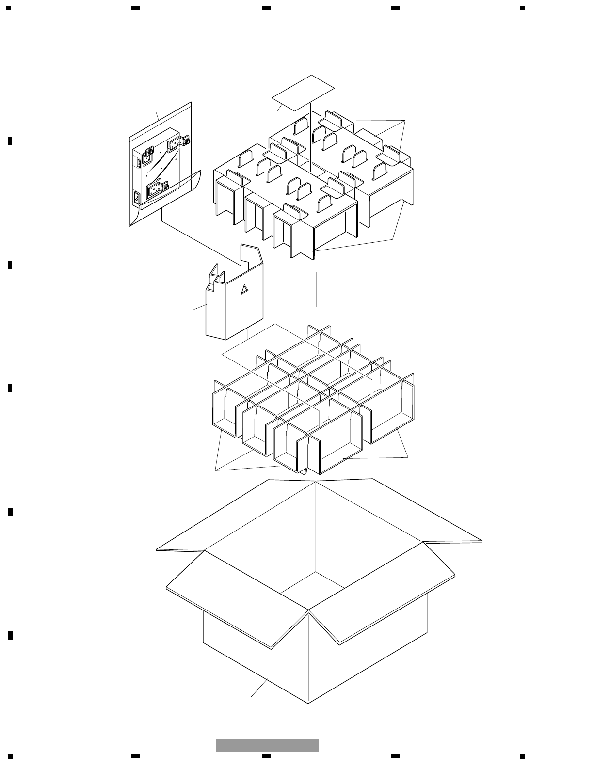
2. EXPLODED VIEWS AND PARTS LIST
2.1 PACKING

5
5
6
7
8
F
E
D
C
B
A
5
6
7
8
GEX-M7027XMZH/XN/UC
NOTE:
- Parts marked by “*” are generally unavailable because they are not in our Master Spare Parts List.
- Screws adjacent to ∇ mark on the product are used for disassembly.
- For the applying amount of lubricants or glue, follow the instructions in this manual.
( In the case of no amount instructions, apply as you think it appropriate.)
- PACKING SECTION PARTS LIST
Mark No. Description Part No.
1 Contain Box CHL4928
2 Protector CHP2656
3 Protector CHP2657
4 Polyethylene Bag CEG1297
5 Protector CHP2655
* 6 Card CRL2374

6
1
1
24
1
1
3
2
20
26
8
21
19
4
10
15
12
13
17
17
11
14
16
1
1
1
1
1
1
1
26
26
9
28
5
23
6
7
22
27
25
18
A
B
C
1
234
12
34
F
E
D
C
B
A
GEX-M7027XMZH/XN/UC
2.2 EXTERIOR

1 Screw BSZ30P060FTC
2 Tape CNM8263
3 Cushion CNM8321
4 Main Unit CWM8561
5 Connector(CN901) CKM1208
6 Connector(CN501) CKS4065
7 Connector(CN502) CKS4065
8 Holder CND1263
9 Holder CND1284
10 RF Unit CWE1683
11 Connector(CN2) CKS4667
12 Connector(CN1) CKX1068
13 Case CND1264
14 Holder CND1265
15 Holder CND1266
16 Insulator CNM7993
17 Screw PRZ30P060FTC
18 Digital Unit CWX2749
19 Connector(CN201) CKS4667
20 Case CND1267
21 Holder CND1268
22 Terminal(CN801) VNF1084
23 Terminal(CN802) VNF1084
24 Case Unit CXB9640
25 Chassis Unit CXB9753
26 Screw ISS26P055FTC
27 Power Supply Unit
(U801) CWR1072
28 Transistor(Q852) 2SB1185
7
5
6
7
8
F
E
D
C
B
A
5
6
7
8
GEX-M7027XMZH/XN/UC
Mark No. Description Part No.
- EXTERIOR SECTION PARTS LIST

8
IC 1
AT-119
IC 3
MAX2644EXT
33
IC 6
MAX2644EXT
63
IC 7
SW-475
15
IC 2
AT-119
IC 4
MAX2644EXT
33
IC 5
MAX2644EXT
63 125
4
4
IC 10
AD8314ARM
7
IC 15
S-812C25AMC-C2F
3
3
RF AGC DETECTOR
KEYED AGC CIRCUIT
F2
7
IC 11
MAX2682EUT
3 4
1
F4
5
IC 17
AD61009ARS
14
6
F1
IC 9
MAX2682EUT
3 4
F16
5
IC 18
AD61009ARS
14
6
F3
IC 14
RF2325
3
5
1st IF (TER)
1st IF (SAT)
2nd MIX AND AGC AMP
2nd MIX AND AGC AMP
IC 12
RF2326
5
3
1
IC 13
SI4136XM-BT
11
IC 8
AD8061ART
IC 16
TC7W14FK
13
1
23.920MHZ
3
SYS_CLK
1
15
2
3
17
9
8
2
3
16 9
17
9
8
ANTENNA
SELECT CIRCUIT
2.5GHz AND IF PLL
4
4
22
TER_IF2
SAT_IF2
5
CTL
12
SAT_AGC
12
TER_AGC
TERRESTRIAL BRANCH
SATELLITE BRANCH
CN1
SAT_IN
TER_IN
1
1
RF UNIT
11
15
22
3
7
6
CN2
26
28
30
VCC
VCC_2
VCC_2
X1
B
10
12
14
16
6
4
2
1
IC 202
STA-400
5
8
DIGITAL UNIT
2
CN201
CDEC
IC 206
STA-450
SSDEC
IC 201
AD8131ARM
1
20
IF2SA_N
IF2TA_N
15
IC 203
K4S280832D-TL1H
SDRAM
83
34
PCSD1
PCSD
6
5
30
SAGC
TAGC
29
SAT_IF
TER_IF
SAT_AGC
TER_AGC
IC 204
TC7SH86FU
MOBILE
ADAPTER CIRCUIT
30
XTI/MCLK
33 SYS_CLK
IC 207
PCM1716E-3
2
73
SDO
16
AUDIO_L
27
DAC
CN502
CN
11
15
22
3
7
6
1
2
5
6
30
27
SY
TE
SA
CT
SA
TE
SAT_IF2
TER_IF2
SAT_AGC
TER_AGC
SYS_CLK
LCH
IC 702
S-80827ANUP-EDQ
1
BU3R3V
2
RESET
26
28
29
262826
28
D3R3V
VCC3.3V
202220
22
D2R5V
VCC2.5V
24 24
X601
10.00MHz
MAIN UNIT
29 29 DAC5V
AUDIO5V
A
IC 205
ST19AF08BR20QMAA
C
10
12
14
16
4
IF2TA_P
14
LCH
DIN
1
234
12
34
F
E
D
C
B
A
GEX-M7027XMZH/XN/UC
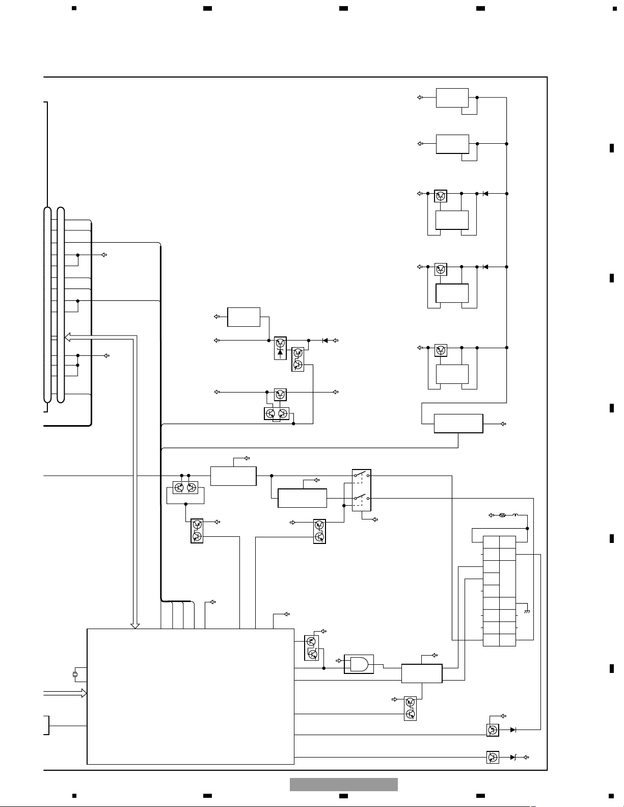
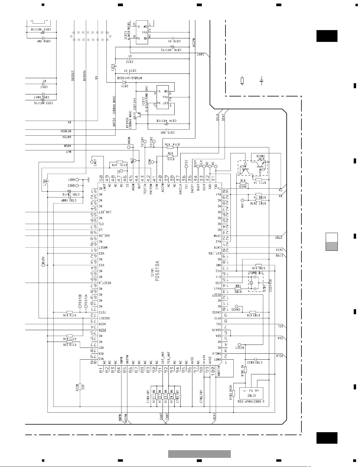
3. BLOCK DIAGRAM AND SCHEMATIC DIAGRAM
3.1 BLOCK DIAGRAM
9
11
15
22
3
7
6
26
28
30
10
12
14
16
CN501
11
15
22
3
7
6
SYS_CLK
TER_IF2
SAT_IF2
CTL
SAT_AGC
TER_AGC
75
bsen
74
ASEN
1
57
CTL
IC 401
NJM4558MD
6
7
IC 601
PD5818A
SYSTEM CONTROLLER
91
SAT_ANT
92
TER_ANT
84
XMPW
26
28
29
RF3R3V
13
15
XOUT
XIN
X601
10.00MHz
MUT
44
10
12
14
16
TER_ANT
IC 402
NJM4558MD
6
7
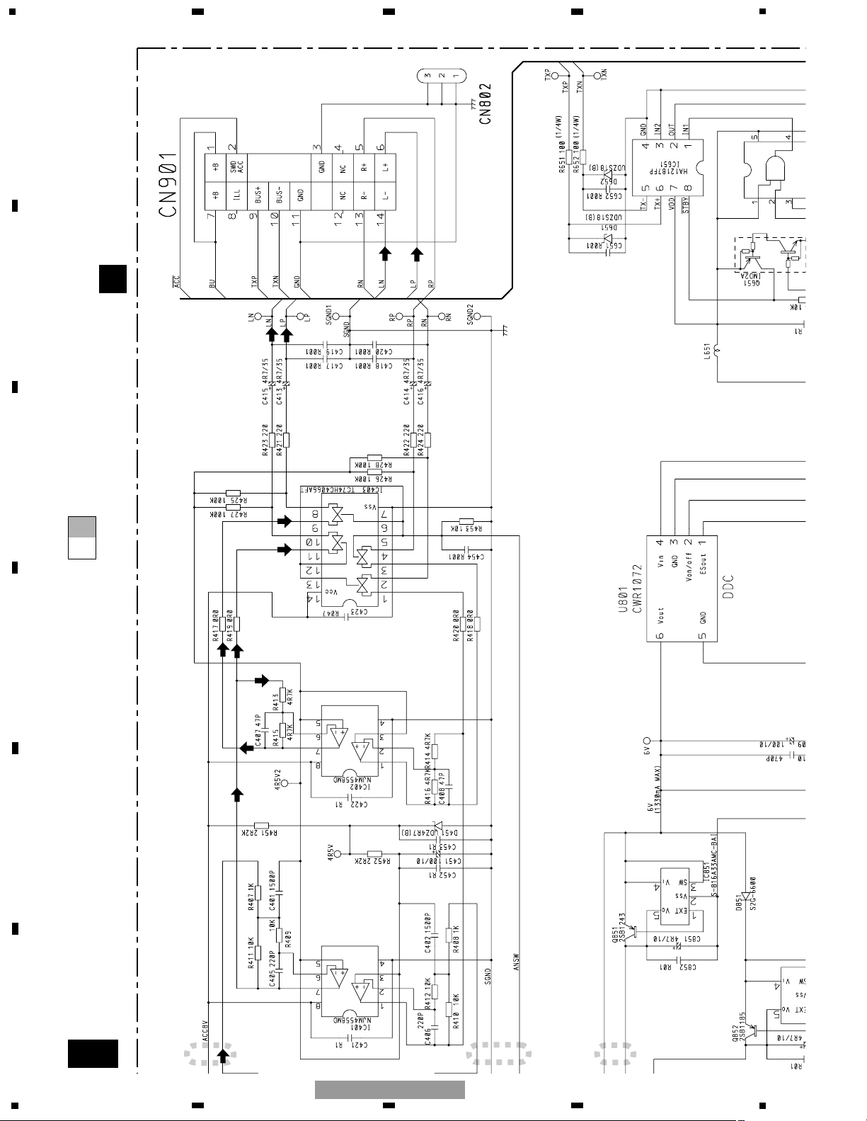
IC 651
HA12187FP
1
25
6
Q451
ACC8V
Q452
ACC8V
ANSW
45
11 10
12
9
6
8
LN
LP
MUTE
LCH
Q401
TXP
TXN
TX+
TX-
TX
RX
TX
RX1
30
29
BU13
Q605
Q601
BU3R3V
BU13V
CTL
U801
6
4
BU13
6V
Q851
IC 851
1
5
S-816A33AMC-BAI
4
3
D3R3V
6V
Q852
IC 852
1
5
S-816A25AMC-BAA
4
3
D2R5V
6V
IC 871
4
NJM2870F05
5
1
ANT5V
6V
IC 853
4
NJM2870F05
5
1
DAC5V
6V
Q873
IC 872
1
5
S-816A33AMC-BAI
4
3
RF3R3V
6V
Q951
5V BU13V
Q952
ACCPW
8V BU13V
Q972
IC 951
4
S-812C33AUA-C2N
5
BU3R3V
Q971
DIGITAL 3.3V REGULATOR
DIGITAL 2.5V REGULATOR
RF3.3V REGULATOR
DAC5V REGULATOR
ANT5V REGULATOR
DC/DC CONVERTER
2
XMPW
reset
12
Q701
TXD
31
BU3R3V
Q651
5V
8 stby
IPPW
22
40
ACCPW
BU 3.3V REGULATOR
BU 5V REGULATOR
AUDIO 8V REGULATOR
IC 403
TC74HC4066AFT
ANT5V
ANT5V
8V
8
8V
8
8V
14
5V
7
BU3R3V
VDD
62
A SENSE
B SENSE
GA-NET DRIVER
LEVEL SHIFT
IC 652
TC7SET08FU
1
2
4
5V
GND
NC
NC
+B
+B
ILL
SWD
ACC
BUS+
BUS-
GND
R-
R+
L-
L+
8
7
10
9
12
11
14
13
2
1
4
3
6
5
5
6
7
8
F
E
D
C
B
A
5
6
7
8
GEX-M7027XMZH/XN/UC
A-a A-b
A-a
A-b
A-b
A-a
Large size
SCH diagram
Guide page
Detailed page
Note: When ordering service parts, be sure to refer to " EXPLODED VIEWS AND PARTS LIST" or
"ELECTRICAL PARTS LIST".
A-a
A
B
CN2
C
CN201
Symbol
No diffe
discrete
NOTE :
Symbol
No diffe
discrete
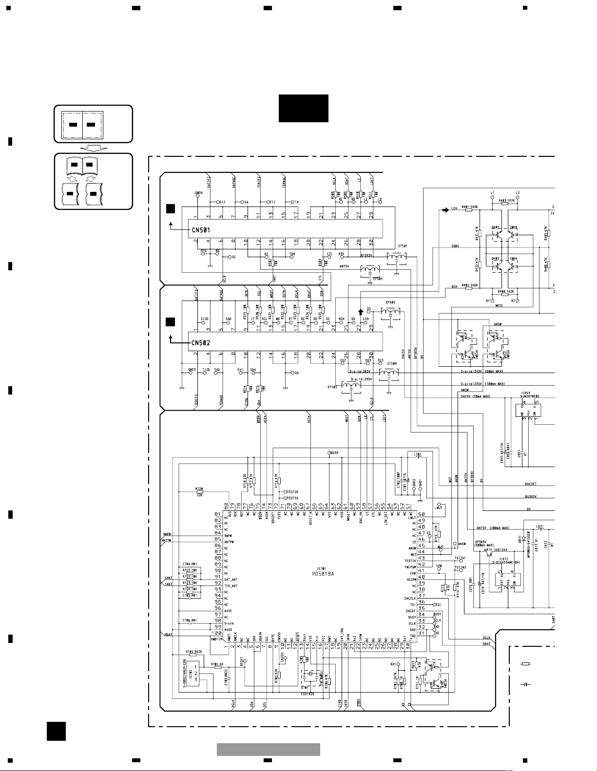
MICRO COMPUTER
ANT
CHECK
RESET
LEVEL SHIFT
RF UNIT
3.3V
DAC 5V
MUTE
36
52
41
41
52
36
3
6
5
2
4
1
3
6
5
2
4
1
3
6
5
2
4
1
10
1
234
12
34
F
E
D
C
B
A
GEX-M7027XMZH/XN/UC
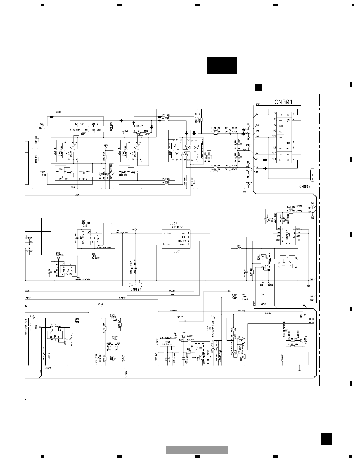
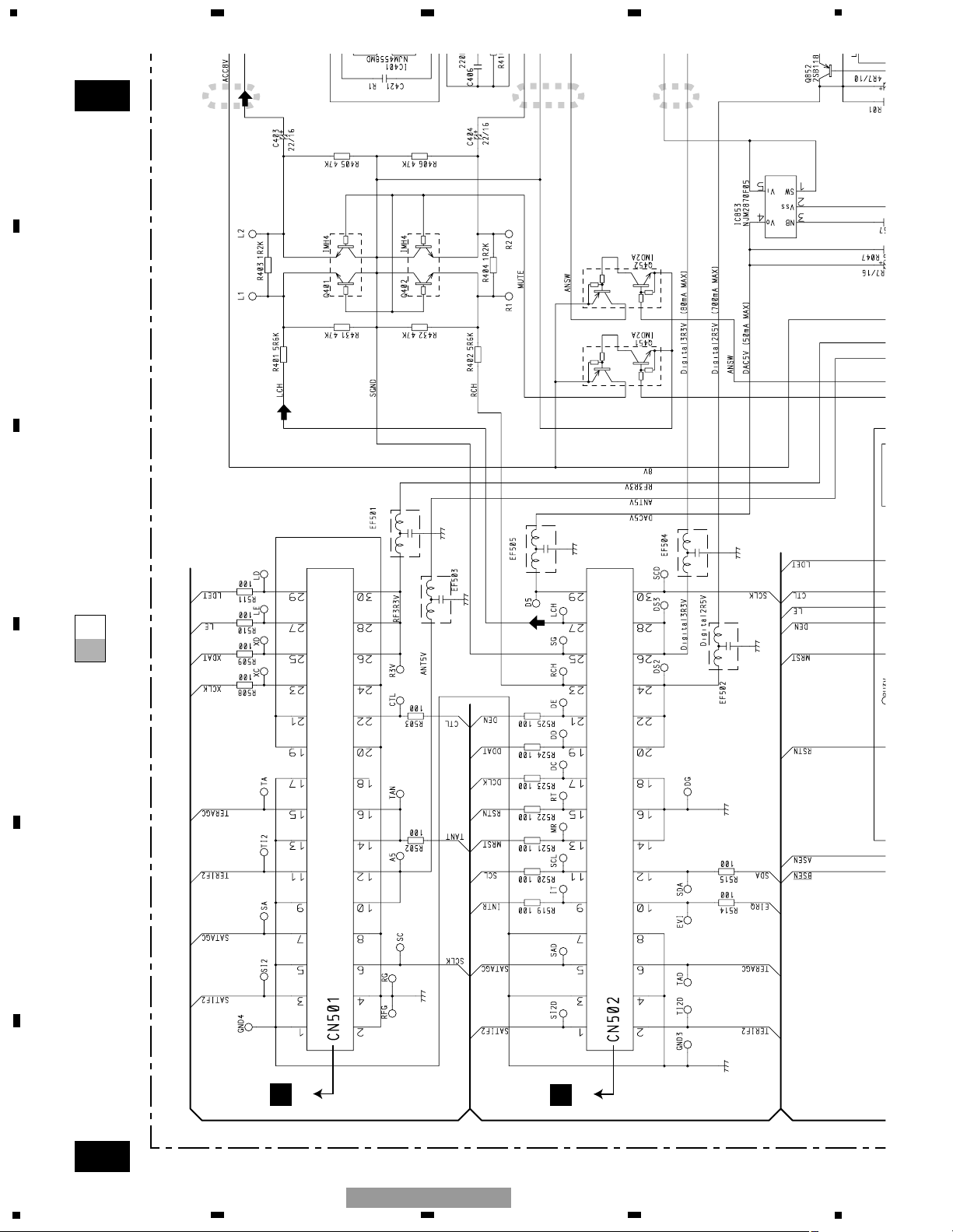
3.2 OVERALL CONNECTION DIAGRAM(GUIDE PAGE)
A-b
A
C656
R1
IC651
TC7SET08FU
A
MAIN UNIT
Decimal points for resistor
and capacitor fixed values
are expressed as :
2.2 2R2
0.022 R022
←
←
Symbol indicates a resistor.
No differentiation is made between chip resistors and
discrete resistors.
TE :
Symbol indicates a capacitor.
No differentiation is made between chip capacitors and
discrete capacitors.
ANT 5V
AUDIO 8V
B.UP
3.3V
B.UP 5V
ASENSE
BSENSE
GA-net
BUS DRIVER
DC-DC CONVERTER
6V
DIGITAL UNIT 3.3V
DIGITAL UNIT 2.5V
C 5V
3
6
5
2
4
1
3
6
5
2
4
1
36
52
41
11
5
6
7
8
F
E
D
C
B
A
5
6
7
8
GEX-M7027XMZH/XN/UC
A-a
A-b
A-a
A-a
A-b
1
2
3
B
CN2
C
CN201
DIGITAL
DAC 5V
MUTE
36
52
41
41
52
36
3
6
524
1
3
6
524
1
12
1
234
12
34
F
E
D
C
B
A
GEX-M7027XMZH/XN/UC
A-a
A-b
A-a
A-a
A-b
4
Symbol indicates a re
No differentiation is m
discrete resistors.
NOTE :
Symbol indicates a ca
No differentiation is m
discrete capacitors.
MICRO COMPUTER
ANT
CHECK
RESET
LEVEL SHIFT
RF UNIT
3.3V
ANT 5V
3
6
5
241
13
5
6
7
8
F
E
D
C
B
A
5
6
7
8
GEX-M7027XMZH/XN/UC
A-a
A-b
A-b
1
2
3
IC651
TC7SET08FU
A
MAIN UNIT
GA-net
BUS DRIVER
DC-DC CONVERTER
6V
DIGITAL UNIT 3.3V
DIGITAL UNIT 2.5V
3
524
1
14
1
234
12
34
F
E
D
C
B
A
GEX-M7027XMZH/XN/UC
A-a
A-b
A-b
4
C656
R1
Decimal points for resistor
and capacitor fixed values
are expressed as :
2.2 2R2
0.022 R022
←
←
ANT 5V
AUDIO 8V
B.UP
3.3V
B.UP 5V
ASENSE
BSENSE
6
5
4
1
3
6
524
1
36
52
41
15
5
6
7
8
F
E
D
C
B
A
5
6
7
8
GEX-M7027XMZH/XN/UC
B-a
B
ANTENNA SELECT
B
RF UNIT
16
1
234
12
34
F
E
D
C
B
A
GEX-M7027XMZH/XN/UC
3.3 RF UNIT(GUIDE PAGE)

B-b
B
A
CN501
17
5
6
7
8
F
E
D
C
B
A
5
6
7
8
GEX-M7027XMZH/XN/UC

A-a
B-b
B-a
B-a
B-b
1
2
ANTENNA SELECT
B
RF UNIT
18
1
234
12
34
F
E
D
C
B
A
GEX-M7027XMZH/XN/UC
A-a
B-b
B-a
B-a
B-b
3
4
19
5
6
7
8
F
E
D
C
B
A
5
6
7
8
GEX-M7027XMZH/XN/UC
 Loading...