

Page 1

PIONEER CORPORATION 4-1, Meguro 1-chome, Meguro-ku, Tokyo 153-8654, Japan
PIONEER ELECTRONICS (USA) INC. P.O. Box 1760, Long Beach, CA 90801-1760, U.S.A.
PIONEER EUROPE NV Haven 1087, Keetberglaan 1, 9120 Melsele, Belgium
PIONEER ELECTRONICS ASIACENTRE PTE. LTD. 253 Alexandra Road, #04-01, Singapore 159936
PIONEER CORPORATION 2002
ORDER NO.
CRT2874
GEX-6100TV/UC
HIDE-A WA Y TV TUNER
GEX-6100TV
HIDE-A WA Y TV TUNER
GEX-6100TVP
EW
UC
For details, refer to "Important symbols for good services".
K-ZZA.MAY 2002.printed in Japan
Page 2

1234
SAFETY INFORMATION
UC
A
CAUTION
This service manual is intended for qualified service technicians; it is not meant for the casual do-it-yourselfer.
Qualified technicians have the necessary test equipment and tools, and have been trained to properly and safely repair
complex products such as those covered by this manual.
Improperly performed repairs can adversely affect the safety and reliability of the product and may void the warranty.
If you are not qualified to perform the repair of this product properly and safely, you should not risk trying to do so
and refer the repair to a qualified service technician.
WARNING
This product contains lead in solder and certain electrical parts contain chemicals which ar
California to cause cancer, birth defects or other reproductive harm.
Health & Safety Code Section 25249.6 - Proposition 65
B
C
e known to the state of
D
2
1234
GEX-6100TV/UC
Page 3
A
B
5678
[ Important symbols for good services ]
In this manual, the symbols shown-below indicate that adjustments, settings or cleaning should be made securely.
When you find the procedures bearing any of the symbols, be sure to fulfill them:
1. Product safety
You should conform to the regulations governing the product (safety, radio and noise, and other regulations), and
should keep the safety during servicing by following the safety instructions described in this manual.
2. Adjustments
To keep the original performances of the product, optimum adjustments or specification confirmation is indispensable.
In accordance with the procedures or instructions described in this manual, adjustments should be performed.
3. Cleaning
For optical pickups, tape-deck heads, lenses and mirrors used in projection monitors, and other parts requiring cleaning,
proper cleaning should be performed to restore their performances.
4. Shipping mode and shipping screws
To protect the product from damages or failures that may be caused during transit, the shipping mode should be set or
the shipping screws should be installed before shipping out in accordance with this manual, if necessary.
5. Lubricants, glues, and replacement parts
Appropriately applying grease or glue can maintain the product performances. But improper lubrication or applying
glue may lead to failures or troubles in the product. By following the instructions in this manual, be sure to apply the
prescribed grease or glue to proper portions by the appropriate amount.For replacement parts or tools, the prescribed
ones should be used.
C
GEX-6100TV/UC
56
D
3
7
8
Page 4

1234
CONTENTS
SAFETY INFORMATION. . . . . . . . . . . . . . . . . . . . . . . . . . . . . . . . . . . . . . . . . . . . .2
1. SPECIFICATIONS . . . . . . . . . . . . . . . . . . . . . . . . . . . . . . . . . . . . . . . . . . . . . . . 5
2. EXPLODED VIEWS AND PARTS LIST . . . . . . . . . . . . . . . . . . . . . . . . . . . . . . . . . . . . 6
2.1 PACKING . . . . . . . . . . . . . . . . . . . . . . . . . . . . . . . . . . . . . . . . . . . . . . . . . 6
A
B
2.2 EXTERIOR. . . . . . . . . . . . . . . . . . . . . . . . . . . . . . . . . . . . . . . . . . . . . . . . . 8
3. BLOCK DIAGRAM AND SCHEMATIC DIAGRAM . . . . . . . . . . . . . . . . . . . . . . . . . . . . . . 10
3.1 BLOCK DIAGRAM. . . . . . . . . . . . . . . . . . . . . . . . . . . . . . . . . . . . . . . . . . . . 10
3.2 OVERALL CONNECTION DIAGRAM(GUIDE PAGE)(GEX-6100TV/UC) . . . . . . . . . . . . . . . . 12
3.3 OVERALL CONNECTION DIAGRAM(GUIDE PAGE)(GEX-6100TVP/EW) . . . . . . . . . . . . . . . 18
4. PCB CONNECTION DIAGRAM . . . . . . . . . . . . . . . . . . . . . . . . . . . . . . . . . . . . . . . 24
4.1 TV TUNER PCB . . . . . . . . . . . . . . . . . . . . . . . . . . . . . . . . . . . . . . . . . . . . . 24
4.2 CONNECTOR PCB . . . . . . . . . . . . . . . . . . . . . . . . . . . . . . . . . . . . . . . . . . . 26
5. ELECTRICAL PARTS LIST . . . . . . . . . . . . . . . . . . . . . . . . . . . . . . . . . . . . . . . . . 27
6. ADJUSTMENT . . . . . . . . . . . . . . . . . . . . . . . . . . . . . . . . . . . . . . . . . . . . . . . . 32
7. GENERAL INFORMATION. . . . . . . . . . . . . . . . . . . . . . . . . . . . . . . . . . . . . . . . . . 35
7.1 DIAGNOSIS . . . . . . . . . . . . . . . . . . . . . . . . . . . . . . . . . . . . . . . . . . . . . . . 35
7.1.1 DISASSEMBLY . . . . . . . . . . . . . . . . . . . . . . . . . . . . . . . . . . . . . . . . . . . . 35
7.1.2 CONNECTOR FUNCTION DESCRIPTION . . . . . . . . . . . . . . . . . . . . . . . . . . . . . . 36
7.2 IC . . . . . . . . . . . . . . . . . . . . . . . . . . . . . . . . . . . . . . . . . . . . . . . . . . . . 37
8. OPERATIONS . . . . . . . . . . . . . . . . . . . . . . . . . . . . . . . . . . . . . . . . . . . . . . . . 39
C
D
4
1234
GEX-6100TV/UC
Page 5

A
B
5678
1. SPECIFICATIONS
- GEX-6100TV/UC
General
Power source ............................................................................................................................................ 9.0 V DC
Grounding system .............................................................................................................................. Negative type
Max. current consumption .............................................................................................................................. 0.5 A
Dimensions ............................................................................................................ 82 (W) × 28 (H) × 166 (D) mm
............................................................................................................[3-1/4 (W) × 1−1/8 (H) × 6−1/2 (D) in.]
Weight ............................................................................................................................................ 0.35 kg [0.8 lbs]
Backup current ...............................................................................................................................................
TV tuner
Reception channel/TV system .............................................................. US/M: VHF 2 — 13 ch, UHF 14 — 69 ch
Color system ....................................................................................................................................NTSC compatible
Usable sensitivity .................................................................................................................... 14 dBµ (75 Ω, mono)
Video S/N ................................................................................ Over 37 dB (59 dBµ RF input, White Peak 100%)
Video S/N 30 dB usable sensitivity ............................................................................................................ 46 dBµ
Antenna input ........................................................................................................ 1 ch (φ 3.5 mm Mini plug type)
Antenna cable ...................................................................................................................................... 6 m [236 in.]
0 mA
Note:
• Specifications and the design are subject to possible modification without notice due to improvements.
- GEX-6100TVP/EW
General
Power source ............................................................................................................................................ 9.0 V DC
Grounding system .............................................................................................................................. Negative type
Max. current consumption .............................................................................................................................. 0.5 A
Dimensions ............................................................................................................ 82 (W) × 28 (H) × 166 (D) mm
Weight .......................................................................................................................................................... 0.35 kg
Backup current ...............................................................................................................................................
0 mA
TV tuner
Reception channel/TV system .................... COUNTRY 1: (CCIR/B, G, H) : VHF 2 — 12 ch, UHF 21 — 69 ch
(For each Country Group) COUNTRY 2: (ITALY/B, G, H) : VHF A — H2 ch, UHF 21 — 69 ch
Color system .................................................................................................................................... PAL compatible
Usable sensitivity .................................................................................................................... 14 dBµ (75 Ω, mono)
Video S/N ................................................................................ Over 37 dB (59 dBµ RF input, White Peak 100%)
Video S/N 30 dB usable sensitivity ............................................................................................................ 46 dBµ
Antenna input ........................................................................................................ 1 ch (φ 3.5 mm Mini plug type)
Antenna cable .................................................................................................................................................... 6 m
COUNTRY 3: (UK, IRELAND/I) : VHF A — K ch, UHF 21 — 69 ch
COUNTRY 4: (OIRT/D, K) : VHF R1 — R12 ch, UHF 21 — 69 ch
C
Note:
• Specifications and the design are subject to possible modification without notice due to improvements.
GEX-6100TV/UC
56
7
D
5
8
Page 6
1234
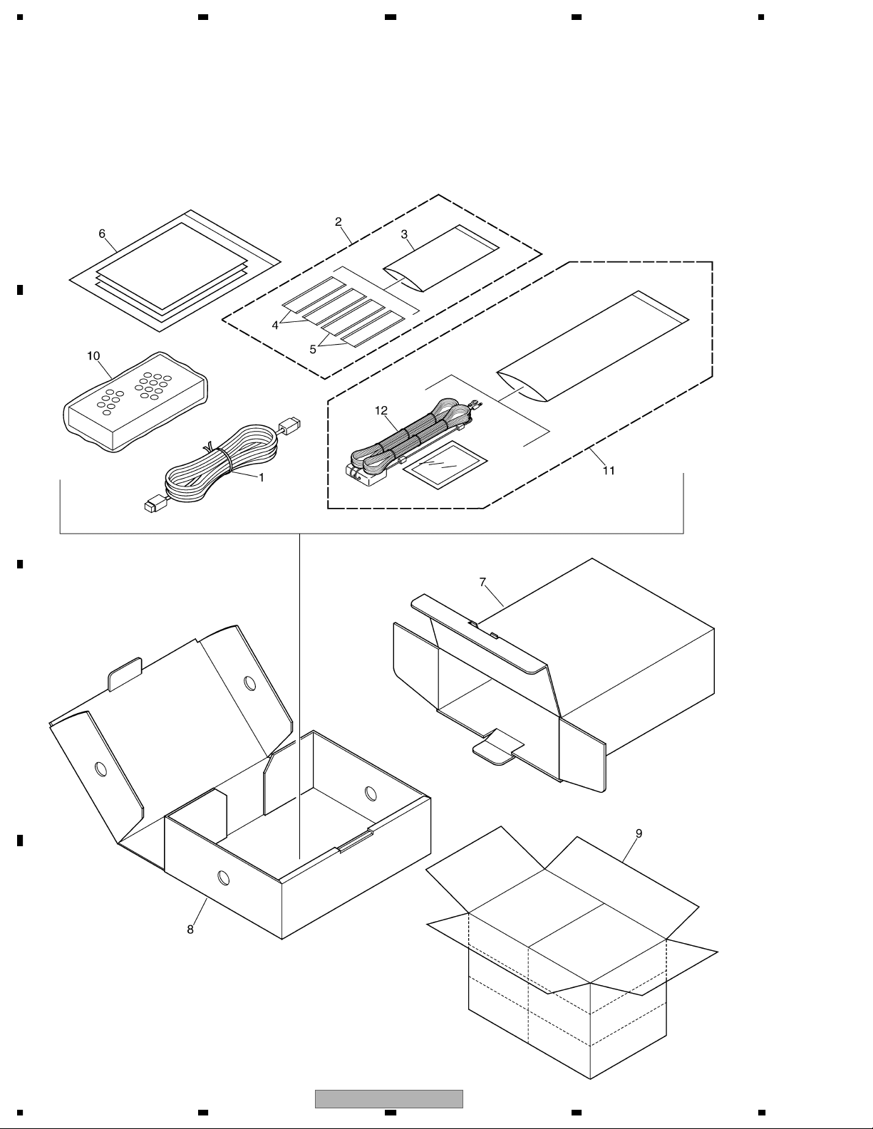
2. EXPLODED VIEWS AND PARTS LIST
NOTES : • Parts marked by " * " are generally unavailable because they are not in our Master Spare Parts List.
• Screw adjacent to mark on the product are used for disassembly.
• For the applying amount of lobricants or glue, follow the instructions in this manual.
A
(In the case of no amount instructions,apply as you think it appropriate.)
"
2.1 PACKING
B
C
D
6
1234
GEX-6100TV/UC
Page 7
A
B
5678
(1) PACKING SECTION PARTS LIST
Mark
No. Description Part No.
1 Cord Assy CDE6817
2 Accessory Assy CEA2657
* 3 Polyethylene Bag CEG1101
4 Fastener(Rough) CNM6888
5 Fastener(Soft) CNM6889
6-1 Polyethylene Bag CEG1116
6-2 Owner's Manual See Contrast table(2)
* 6-3 Warranty Card See Contrast table(2)
Mark No. Description Part No.
* 6-4 Card See Contrast table(2)
7 Carton See Contrast table(2)
8 Sub Carton CHG4725
9 Contain Box See Contrast table(2)
10 Air Cushioned Bag CEG1143
11 Antenna Assy CXB9219
12 Antenna Unit CZX5019
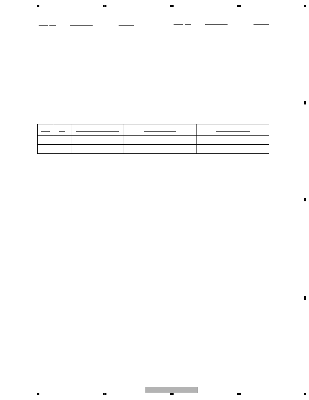
(2) CONTRAST TABLE
GEX-6100TV/UC and GEX-6100TVP/EW are constructed the same except for the following:
k NO Symbol and Description GEX-6100TV/UC GEX-6100TVP/EW
Mar
6-2 Owner's Manual CRD3641 CRD3657
* 6-3 Warranty Card Not used CRY1157
* 6-4 Card ARY1048 Not used
7 Carton CHG4723 CHG4724
9 Contain Box CHL4723 CHL4724
Owner's Manual,Installation Manual
Part No. Language
CRD3641 English, French, Spanish
CRD3657 English, Spanish, German, French, Italian, Dutch
C
GEX-6100TV/UC
56
D
7
7
8
Page 8
1234
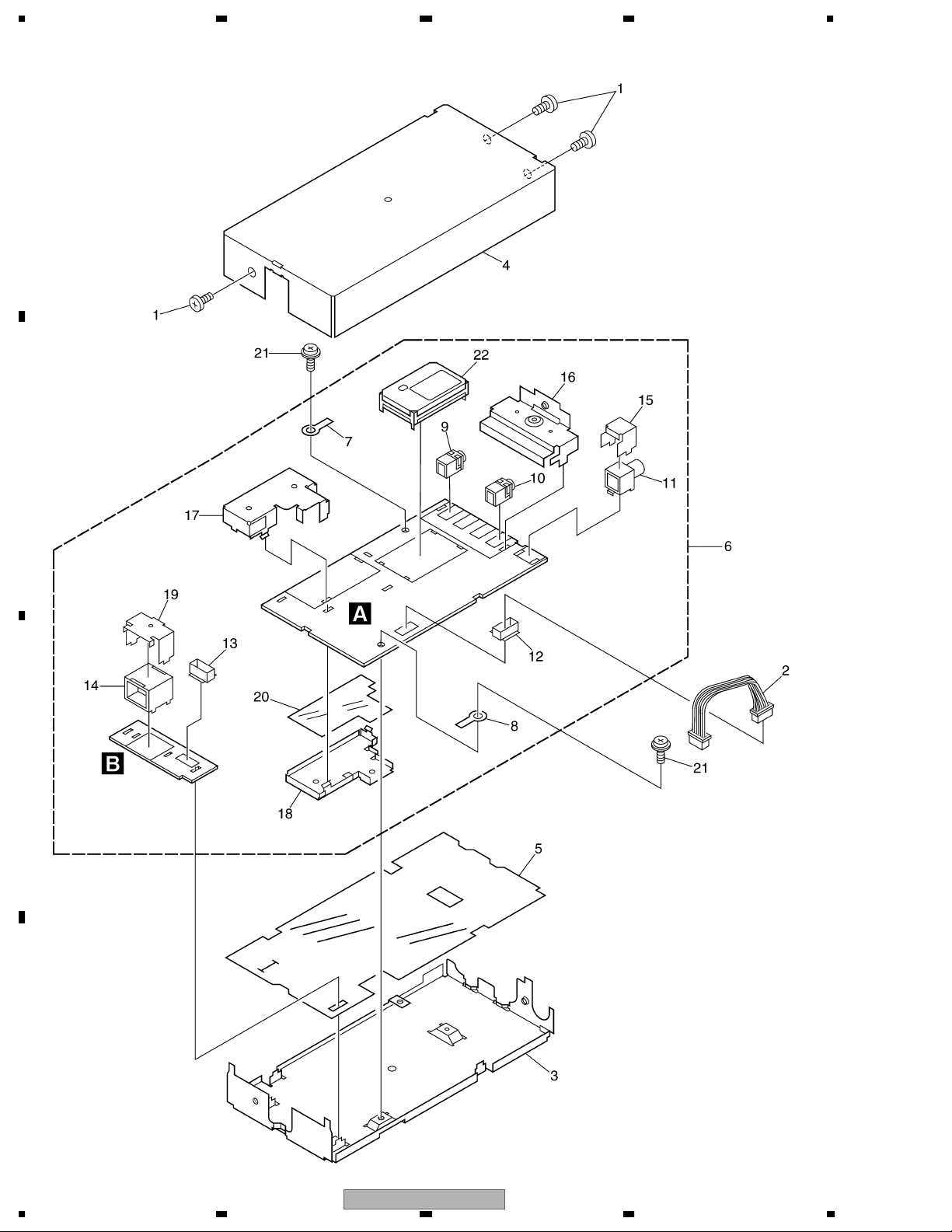
2.2 EXTERIOR
A
B
C
D
8
1234
GEX-6100TV/UC
Page 9
A
B
5678
(1) EXTERIOR SECTION PARTS LIST
Mark
No. Description Part No.
1 Screw BSZ30P060FMC
2 Cord Assy CDE6843
3 Chassis CNA2504
4 Case CNB2748
5 Insulator CNM7712
6 Tuner Unit See Contrast table(2)
7 Terminal(CN2201) CKF1064
8 Terminal(CN2601) CKF1064
9 Jack(CN2150) CKN1032
10 Jack(CN2153) CKN1032
11 Pin Jack(CN2703) CKS1825
Mark No. Description Part No.
12 Connector(CN2701) CKS4587
13 Connector(CN2704) CKS4587
14 Connector(CN2705) CKS4598
15 Holder CNC6746
16 Holder CNC9253
17 Shield CNC9885
18 Shield CNC9886
19 Holder CND1097
20 Insulator CNM7680
21 Screw ISS26P055FUC
22 Front End(FE2201) See Contrast table(2)
(2) CONTRAST TABLE
GEX-6100TV/UC and GEX-6100TVP/EW are constructed the same except for the following:
k NO Symbol and Description GEX-6100TV/UC GEX-6100TVP/EW
Mar
6 Tuner Unit CWM8251 CWM8249
22 Front End(FE2201) CWB1093 CWB1094
C
GEX-6100TV/UC
56
D
9
7
8
Page 10
1234
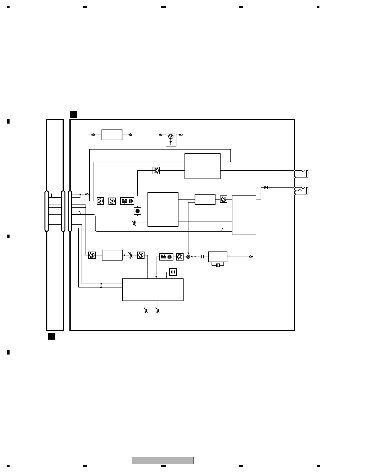
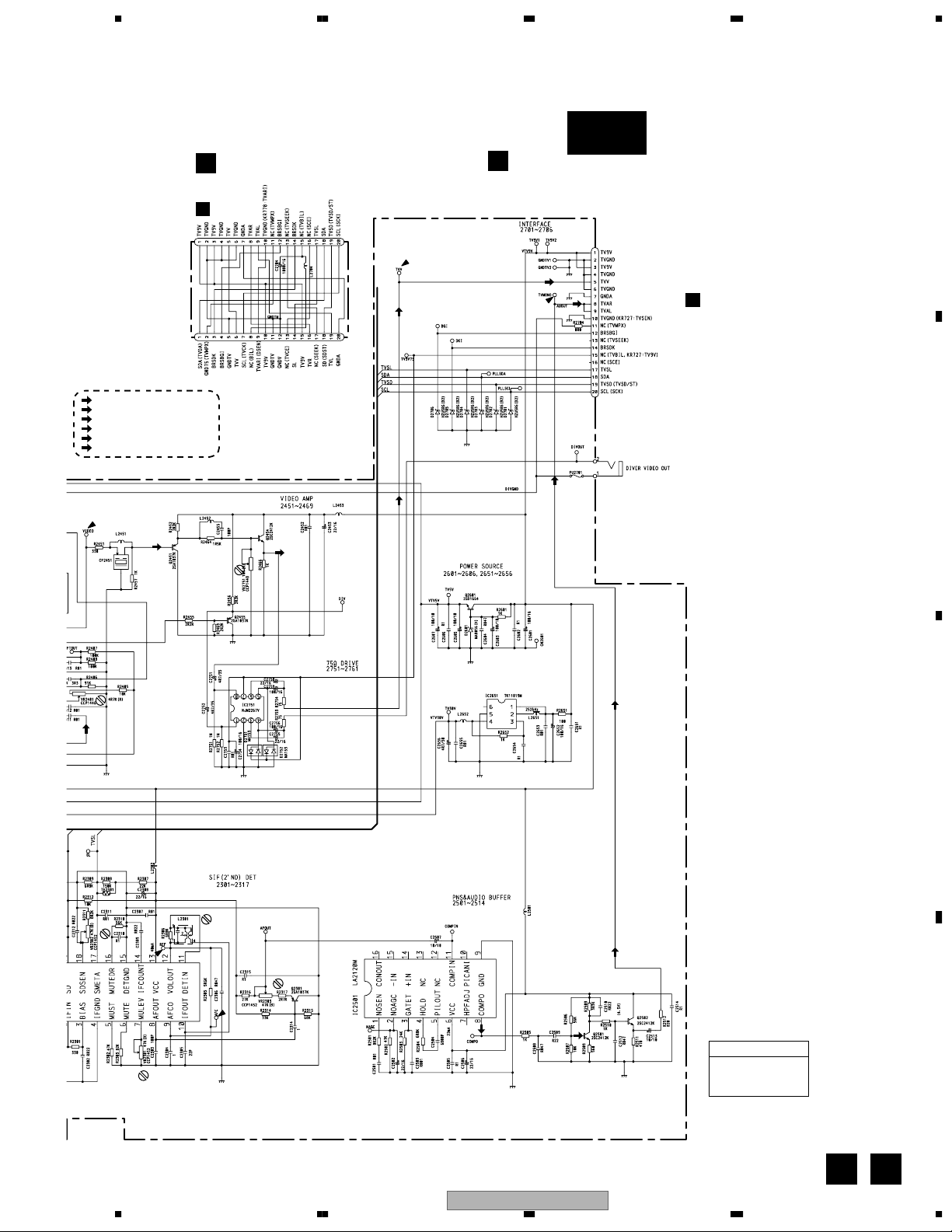
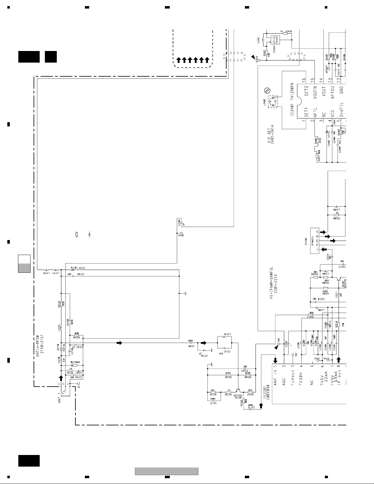
3. BLOCK DIAGRAM AND SCHEMATIC DIAGRAM
3.1 BLOCK DIAGRAM
A
- GEX-6100TV/UC
TV TUNER PCB
A
TV30V REG. TV5V REG.
IC 2651
24
TK11819M
TV30VTV9V
TV9V
Q2455
Q2601
TV5V
75Ω DRIVE
8
IC 2751
1
NJM2267V
5
4
CN2703
DIVER VIDEO
OUT
B
CN2704
CN2705
TV9V
10
TV9V
15
TVV
6
TVAR
16
TVAL
19
SDA
1
SCL
7
TVSL
14
TVSD
18
to AVR-W6100 series
C
CN2701
TV9V
Q2501
VIDEO AMP
Q2454
Q2451
IC 2501
LA2120M
L2402
VR2401
AUDIO BUFFER
VR2303
118
17
SMETER
19
SD
L2451CF2451
PNS AND
Q2301
TV9V
1
1
TV9V
3
3
TVV
5
5
TVAR
8
8
TVAL
9
9
SDA
18
18
SCL
20
20
TVSL
17
17
TVSD
19
19
VIF DET
14 9
VOUT
15
VOUTN
1
DET1
IC 2401
TA1290FN
16
DET2
10
AGCDL
8
AFOUT
SIF(2ND)DET
IC 2301
LA1145M
AGCOU
L2353CF2351
2
11 10
IFIN
DETIN
SDSENMULEV
187
L2301
PIF2
PIF1
Q2363
IFOUT
SAWFIL
5
8
3
CF2201
IFAMP
14
Q2201
8
1
ANT inIF out
FE2201
11
2
AGC
9
SDA
10
SCL
2ND LOCMIX
Q2353
Q2354
X2351
30.55MHz
TV5V
CN2150
ANT1
VR2302VR2301
CONNECTOR PCB
B
D
10
GEX-6100TV/UC
1234
Page 11
A
B
5678
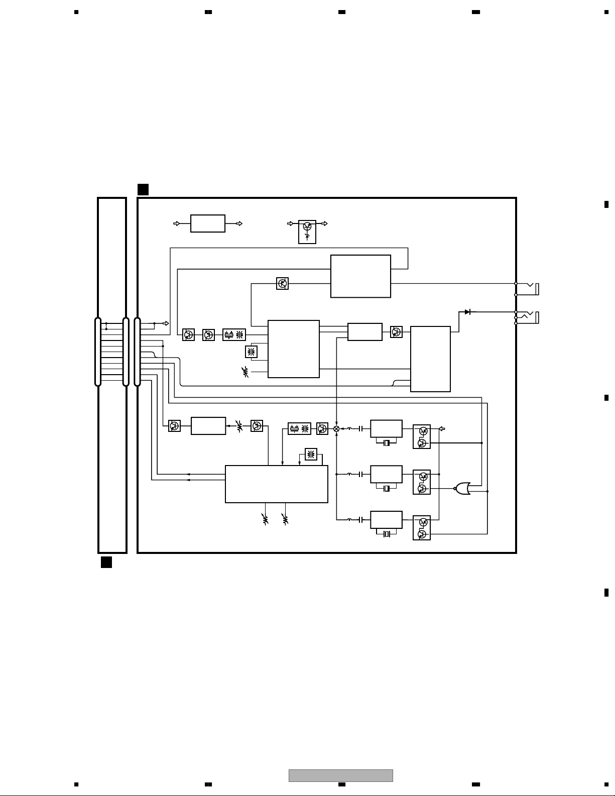
- GEX-6100TVP/EW
TV TUNER PCB
A
CN2704
CN2705
TV9V
10
TV9V
15
TVV
6
TVAR
16
TVAL
19
SDA
1
SCL
7
BRSBGI
4
BRSDK
3
TVSL
14
TVSD
18
to AVR-W6100 series
B
CN2701
TV9V
1
1
TV9V
3
3
TVV
5
5
TVAR
8
8
TVAL
9
9
SDA
18
18
SCL
20
20
BRSBGI
12
12
BRSDK
14
14
TVSL
17
17
TVSD
19
19
CONNECTOR PCB
TV9V
TV30V REG. TV5V REG.
IC 2651
Q2501
2 4
TK11819M
VIDEO AMP
Q2454
Q2451
IC 2501
LA2120M
L2402
VR2401
AUDIO BUFFER
VR2303
118
17
SMETER
19
SD
TV30VTV9V
14 9
L2451CF2451
15
16
10
PNS AND
Q2301
AFOUT
SIF(2ND)DET
LA1145M
1
IC 2301
TV9V
Q2455
VOUT
VOUTN
DET1
DET2
AGCDL
8
VIF DET
IC 2401
TA1290FN
2
IFIN
SDSENMULEV
187
VR2302VR2301
Q2601
PIF2
PIF1
AGCOU
L2353CF2351
L2301
11 10
Q2363
IFOUTDETIN
TV5V
75Ω DRIVE
8
IC 2751
1
NJM2267V
SAWFIL
5
8
3
CF2201
IFAMP
14
5
4
Q2201
DIVER VIDEO
CN2703
CN2150
OUT
ANT1
8
1
ANT inIF out
FE2201
Q2353
Q2354
X2351
Q2357
Q2358
X2352
Q2361
Q2362
X2353
2
AGC
9
SDA
10
SCL
Q2351
TV5V
BRSBGI
Q2352
Q2355
Q2356
Q2359
Q2360
IC 2352
TC7SH02FU
COI
4
BRSDK
2
1
C
11
2ND LOCMIX
22.70MHz
22.20MHz
21.70MHz
GEX-6100TV/UC
56
D
11
7
8
Page 12
C
C
O
C
1234
3.2 OVERALL CONNECTION DIAGRAM(GUIDE PAGE)(GEX-6100TV/UC)
Note: When ordering service parts, be sure to refer to " EXPLODED VIEWS AND PARTS LIST" or
"ELECTRICAL PARTS LIST".
Large size
A-b
A-b
SCH diagram
Guide page
Detailed page
CN2150
RF
RF
RF
A
A-a A-b
A-a
A-a
A-a
NOTE :
Symbol indicates a resistor.
No differentiation is made between chip resistors and
discrete resistors.
Symbol indicates a capacitor.
No differentiation is made between chip capacitors and
discrete capacitors.
The > mark found on some component parts indicates
the importance of the safety factor of the part.
Therefore, when replacing, be sure to use parts of
identical designation.
Decimal points for resistor
and capacitor fixed values
are expressed as :
←
2.2 2R2
←
0.022 R022
CV
COMPOSITE VIDEO
MA
MONAURAL AUDI
RF
RF SIGNAL
PRF
VIDEO IF SIGNAL
SIF
AUDIO IF SIGNAL
IF
IF SIGNAL
B
RF
RF
PIF
IF
PIF
IF
SIF
PIF
SIF SIF
PIF
PIF
PIF
C
D
A
12
GEX-6100TV/UC
1234
Page 13
A
B
CN2704
CN2705
5678
A-b
TV TUNER PCB
CONNECTOR PCB
B
CN2701
A
H
µ
0
0
1
CV
A
CN2701
CV
MA
B
CN2704
CV
COMPOSITE VIDEO SIGNAL
MA
MONAURAL AUDIO SIGNAL(TV AUDIO)
RF
RF SIGNAL
PRF
VIDEO IF SIGNAL
SIF
AUDIO IF SIGNAL
IF
IF SIGNAL
CV
PIF
to AVR-W6100 series
CV
CN2703
MA
CV
MA
C
MA
MA
MA
GEX-6100TV/UC
56
TUNER UNIT
Consists of
TV TUNER PCB
D
CONNECTOR PCB
BA
7
13
8
Page 14
A
U
A
A-b
1234
COMPOSITE VI
MONAURAL A
RF SIGNAL
VIDEO IF SIGN
AUDIO IF SIGN
B
←
←
Decimal points for resistor
and capacitor fixed values
are expressed as :
2.2 2R2
0.022 R022
IF SIGNAL
IF
RF
CV
SIF
MA
PRF
1
2
B
Symbol indicates a resistor.
No differentiation is made between chip resistors and
discrete resistors.
Symbol indicates a capacitor.
No differentiation is made between chip capacitors and
discrete capacitors.
The > mark found on some component parts indicates
the importance of the safety factor of the part.
Therefore, when replacing, be sure to use parts of
A-b
A-a
A-a
identical designation.
NOTE :
PIF
PIF
SIF
IF
C
RF
RF
RF
IF
D
A-a
14
RF
RF
CN2150
GEX-6100TV/UC
1234
Page 15

A
B
5678
PIF
3
A-b
PIF
PIF
PIF
SIF SIF
PIF
PIF
SIF
IF
A-b
A-a
A-a
C
IF
D
GEX-6100TV/UC
56
A-a
7
15
8
Page 16

1234
A
CN2704
B
CN2701
MA
B
CV
CN2703
MA
>
CEK1190
2A
TV TUNER PCB
A
A-b
A-a
CV
C
1
00
µ
H
CV
D
A-b
16
CV
TUNER UNIT
Consists of
TV TUNER PCB
CONNECTOR PCB
CONNECTOR PCB
B
CN2701
A
CN2704
B
CN2705
GEX-6100TV/UC
to AVR-W6100 series
COMPOSITE VIDEO SIGNAL
MONAURAL AUDIO SIGNAL(TV AUDIO)
RF SIGNAL
VIDEO IF SIGNAL
AUDIO IF SIGNAL
IF SIGNAL
IF
RF
RF
CV
SIF
MA
CV
1
2
1234
Page 17

A
B
5678
MA
MA
MA
MA
A-b
A-a
C
PIF
3
GEX-6100TV/UC
56
D
A-b
7
17
8
Page 18

C
C
O
O
1234
3.3 OVERALL CONNECTION DIAGRAM(GUIDE PAGE)(GEX-6100TVP/EW)
A-a
A
CN2150
RF
RF
RF
NOTE :
Symbol indicates a resistor.
No differentiation is made between chip resistors and
discrete resistors.
Symbol indicates a capacitor.
No differentiation is made between chip capacitors and
discrete capacitors.
The > mark found on some component parts indicates
the importance of the safety factor of the part.
Therefore, when replacing, be sure to use parts of
identical designation.
Decimal points for resistor
and capacitor fixed values
are expressed as :
←
2.2 2R2
←
0.022 R022
CV
COMPOSITE VIDE
MA
MONAURAL AUDI
RF
RF SIGNAL
PRF
VIDEO IF SIGNAL
SIF
AUDIO IF SIGNAL
IF
IF SIGNAL
B
RF
RF
PIF
IF
PIF
IF
SIF
PIF
SIF SIF
PIF
PIF
PIF
C
D
A
18
GEX-6100TV/UC
1234
Page 19

A
B
CN2704
CN2705
5678
A-b
TV TUNER PCB
CONNECTOR PCB
B
CN2701
A
H
µ
0
0
1
CV
A
CN2701
CV
MA
B
CN2704
CV
COMPOSITE VIDEO SIGNAL
MA
MONAURAL AUDIO SIGNAL(TV AUDIO)
RF
RF SIGNAL
PRF
VIDEO IF SIGNAL
SIF
AUDIO IF SIGNAL
IF
IF SIGNAL
CV
PIF
to AVR-W6100 series
CV
CN2703
MA
CV
MA
C
MA
MA
MA
GEX-6100TV/UC
56
TUNER UNIT
Consists of
TV TUNER PCB
D
CONNECTOR PCB
BA
7
19
8
Page 20

A
U
A
A-b
1234
COMPOSITE VI
MONAURAL A
RF SIGNAL
VIDEO IF SIGN
AUDIO IF SIGN
B
←
←
Decimal points for resistor
and capacitor fixed values
are expressed as :
2.2 2R2
0.022 R022
IF SIGNAL
IF
RF
CV
SIF
MA
PRF
1
2
B
PIF
PIF
SIF
IF
A-b
A-a
A-a
Symbol indicates a resistor.
No differentiation is made between chip resistors and
discrete resistors.
Symbol indicates a capacitor.
No differentiation is made between chip capacitors and
discrete capacitors.
The > mark found on some component parts indicates
the importance of the safety factor of the part.
Therefore, when replacing, be sure to use parts of
identical designation.
NOTE :
C
RF
RF
RF
IF
D
A-a
20
RF
RF
CN2150
GEX-6100TV/UC
1234
Page 21

A
B
5678
PIF
3
A-b
PIF
PIF
PIF
SIF SIF
PIF
PIF
SIF
IF
A-b
A-a
A-a
C
IF
D
GEX-6100TV/UC
56
A-a
7
21
8
Page 22

1234
A
CN2704
B
CN2701
MA
B
CV
CN2703
>
MA
2A
CEK1190
TV TUNER PCB
A
A-b
A-a
CV
C
1
00
µ
H
CV
D
A-b
22
CV
TUNER UNIT
Consists of
TV TUNER PCB
CONNECTOR PCB
CONNECTOR PCB
B
CN2701
A
CN2704
B
CN2705
GEX-6100TV/UC
to AVR-W6100 series
COMPOSITE VIDEO SIGNAL
MONAURAL AUDIO SIGNAL(TV AUDIO)
RF SIGNAL
VIDEO IF SIGNAL
AUDIO IF SIGNAL
IF SIGNAL
IF
RF
RF
CV
SIF
MA
CV
1
2
1234
Page 23

A
B
5678
MA
MA
MA
MA
A-b
A-a
C
PIF
3
GEX-6100TV/UC
56
D
A-b
7
23
8
Page 24

1234
4. PCB CONNECTION DIAGRAM
4.1 TV TUNER PCB
A
NOTE FOR PCB DIAGRAMS
1. The parts mounted on this PCB
include all necessary parts for
several destination.
For further information for
respective destinations, be sure
to check with the schematic dia gram.
2. Viewpoint of PCB diagrams
Connector
P.C.Board
B
TV TUNER PCB
A
Capacitor
SIDE A
Chip Part
SIDE B
SIDE A
ANTENNA
DIVER VIDEO OUT
TC2110
L2402
C
B
CN2704
L2301
D
A
24
GEX-6100TV/UC
1234
Page 25

A
B
5678
TV TUNER PCB
A
SIDE B
CNT
VDIV5V
AGC
TVV
TVMONO
VIDEO
SD
REF
C
AFC
D
GEX-6100TV/UC
56
A
7
25
8
Page 26

1234
4.2 CONNECTOR PCB
CONNECTOR PCB
A
B
B
to AVR-W6100 series
SIDE A
A
CN2701
CONNECTOR PCB
B
C
D
SIDE B
26
B
GEX-6100TV/UC
1234
Page 27

A
B
5678
5. ELECTRICAL PARTS LIST
NOTE:
• Parts whose parts numbers are omitted are subject to being not supplied.
• The part numbers shown below indicate chip components.
Chip Resistor
RS1/_S___J,RS1/__S___J
Chip Capacitor (except for CQS.....)
CKS....., CCS....., CSZS.....
Circuit Symbol and No. Part Name Part No.
AB
Tuner Unit
Consists of
TV T uner PCB
Connector PCB
Unit Number:CWM8251(GEX-6100/UC)
Unit Name:Tuner Unit
MISCELLANEOUS
IC 2301 IC LA1145M
IC 2401 IC TA1290FN
IC 2501 IC LA2120M
IC 2651 IC TK11819M
IC 2751 IC NJM2267V
Q 2156 T r ansistor 2SC4226
Q 2201 T r ansistor 2SC2735
Q 2301 T r ansistor 2SA1037K
Q 2353 T r ansistor 2SC2735
Q 2354 T r ansistor 2SC2412K
Q 2363 T r ansistor 2SC2735
Q 2451 T r ansistor 2SA1037K
Q 2454 T r ansistor 2SC2412K
Q 2455 T r ansistor 2SA1037K
Q 2501 T r ansistor 2SC2412K
Q 2502 T r ansistor 2SC2412K
Q 2601 T r ansistor 2SD1664
D 2150 Diode HVC136
D 2351 Diode 1SS355
D 2601 Diode MA8056(H)
D 2701 Diode HZU5R6(B2)
D 2702 Diode HZU5R6(B2)
D 2703 Diode HZU5R6(B2)
D 2704 Diode HZU5R6(B2)
D 2705 Diode HZU5R6(B2)
D 2706 Diode HZU5R6(B2)
D 2751 Diode MA153
D 2752 Diode MA153
ZNR2150 Surge Protector RCCA-201Q43UA-PI
L 2150 Inductor LCTC1R0K2125
L 2154 Inductor LCTC1R0K2125
L 2155 Inductor LCKA150J2520
L 2156 Inductor LCYB12NJ1608
L 2157 Inductor CTF1470
L 2161 Inductor LCYB15NJ1608
L 2201 Inductor CTF1470
L 2202 Inductor LCTA2R2J2520
L 2203 Inductor LCTA2R2J2520
L 2204 Inductor CTF1470
L 2205 Inductor LCTC1R5K2125
Circuit Symbol and No. Part Name Part No.
L 2206 Inductor LCTC1R5K2125
L 2207 Inductor LCTC1R5K2125
L 2301 Coil CTC1029
L 2302 Inductor LCKA150J2520
L 2351 Inductor CTF1379
L 2352 Inductor CTF1379
L 2353 Coil CTE1066
L 2356 Inductor LCTC2R2K2125
L 2357 Inductor CTF1379
L 2401 Inductor LCTA2R2J2520
L 2402 Coil CTE1148
L 2451 Inductor LCKA150J2520
L 2452 Inductor LCKA150J2520
L 2453 Inductor LCKA150J2520
L 2501 Inductor LCKA150J2520
L 2651 Transformer CTX1053
L 2652 Inductor LCTC220K2125
L 2704 Choke Coil 100µH CTH1131
TH2301 Thermistor TN20-3U473K
CF2201 SAW Filter CTF1567
CF2351 Filter CTF1057
CF2451 LPF CTF1044
X 2351 Crystal Resonator 30.55MHz CSS1590
VR2301 Semi-fixed 47kΩ(B) CCP1452
VR2302 Semi-fixed 47kΩ(B) CCP1452
VR2303 Semi-fixed 47kΩ(B) CCP1452
VR2401 Semi-fixed 4.7kΩ(B) CCP1446
VR2751 Semi-fixed 10kΩ(B) CCP1448
FU2701 Fuse 2A CEK1190
FE2201 Front End CWB1093
RESISTORS
R 2140 RS1/16S0R0J
R 2150 RS1/16S472J
R 2154 RS1/16S222J
R 2156 RS1/16S472J
R 2157 RS1/16S151J
R 2158 RS1/16S150J
R 2159 RS1/16S151J
R 2160 RS1/16S822J
R 2161 RS1/16S470J
R 2166 RS1/16S0R0J
R 2201 RS1/16S562J
R 2202 RS1/16S102J
R 2203 RS1/16S101J
R 2204 RS1/16S681J
R 2205 RS1/16S101J
R 2206 RS1/16S102J
R 2207 RS1/16S102J
R 2208 RS1/16S102J
R 2209 RS1/16S102J
C
D
GEX-6100TV/UC
56
7
8
27
Page 28

1234
Circuit Symbol and No. Part Name Part No.
R 2210 RS1/16S331J
R 2211 RS1/16S0R0J
R 2212 RS1/16S0R0J
R 2301 RS1/16S331J
R 2302 RS1/16S473J
R 2303 RS1/16S823J
A
R 2305 RS1/16S562J
R 2306 RS1/16S682J
R 2307 RS1/16S223J
R 2308 RS1/16S154J
R 2309 RS1/16S682J
R 2310 RS1/16S563J
R 2311 RS1/16S822J
R 2312 RS1/16S103J
R 2313 RS1/16S103J
R 2314 RS1/16S333J
R 2315 RS1/16S683J
R 2316 RS1/16S273J
R 2317 RS1/16S272J
R 2353 RS1/16S0R0J
R 2354 RS1/16S181J
R 2355 RS1/16S222J
B
R 2356 RS1/16S102J
R 2357 RS1/16S333J
R 2358 RS1/16S683J
R 2360 RS1/16S681J
Circuit Symbol and No. Part Name Part No.
R 2751 RS1/16S105J
R 2752 RS1/16S105J
R 2753 RS1/10S750J
R 2754 RS1/10S750J
CAPACITORS
C 2104 CCSRCH5R0D50
C 2150 CCSRCH470J50
C 2154 CKSRYB103K50
C 2160 CKSRYB103K50
C 2161 CEV100M10
C 2162 CCSRCH5R0D50
C 2166 CCSRCK2R0C50
C 2167 CCSRCKR50C50
C 2169 CKSRYB103K50
C 2171 CKSRYB102K50
C 2172 CKSRYB102K50
C 2201 CKSRYB102K50
C 2202 CKSRYB105K10
C 2203 CKSRYB103K50
C 2204 CKSRYB103K50
C 2205 CCSRCH101J50
C 2206 CKSRYB103K50
C 2207 CCSRCH101J50
C 2209 CEV101M16
C 2210 CKSRYB103K50
R 2385 RS1/16S123J
R 2386 RS1/16S682J
R 2387 RS1/16S561J
R 2388 RS1/16S181J
R 2390 RS1/16S331J
R 2402 RS1/16S472J
R 2403 RS1/16S391J
R 2404 RS1/16S0R0J
R 2405 RS1/16S103J
R 2406 RS1/16S913J
R 2407 RS1/16S104J
R 2408 RS1/16S104J
R 2411 RS1/16S0R0J
R 2451 RS1/16S331J
C
R 2452 RS1/16S222J
R 2455 RS1/16S222J
R 2456 RS1/16S222J
R 2457 RS1/16S102J
R 2464 RS1/16S152J
R 2466 RS1/16S102J
R 2469 RS1/16S222J
R 2501 RS1/16S822J
R 2502 RS1/16S473J
R 2503 RS1/16S243J
R 2504 RS1/16S682J
R 2505 RS1/16S102J
R 2506 RS1/16S563J
R 2507 RS1/16S103J
R 2508 RS1/16S332J
R 2509 RS1/16S561J
D
R 2510 RS1/16S102J
R 2511 RS1/16S471J
R 2512 RS1/16S821J
R 2601 RS1/16S102J
R 2651 RS1/16S101J
C 2211 CKSRYB103K50
C 2212 CCSRCH471J50
C 2213 CKSRYB103K50
C 2214 CKSRYB103K50
C 2301 CKSRYB103K50
C 2302 CKSRYB223K50
C 2303 CCSRCH101J50
C 2304 CKSRYB105K10
C 2305 CCSRCH220J50
C 2306 CKSRYB473K50
C 2307 CKSRYB103K50
C 2308 CEV220M16
C 2309 CKSRYB223K50
C 2310 CKSRYB104K16
C 2311 CKSRYB103K50
C 2312 CKSRYB223K50
C 2313 CKSRYB103K50
C 2314 CKSRYB105K10
C 2315 CKSRYB104K16
C 2351 CEV100M10
C 2352 CKSRYB104K16
C 2353 CKSRYB104K16
C 2354 CKSRYB103K50
C 2355 CCSRCH560J50
C 2356 CCSRCH121J50
C 2357 CCSRCH7R0D50
C 2358 CCSRCKR50C50
C 2376 CKSRYB103K50
C 2379 CKSRYB103K50
C 2380 CEV100M10
C 2381 CKSRYB103K50
C 2382 CKSRYB102K50
C 2385 CCSRCK2R0C50
C 2389 CCSRCH101J50
C 2403 CEV470M16
R 2652 RS1/16S102J
R 2704 RS1/16S0R0J
28
1234
C 2404 CKSRYB103K50
C 2405 CKSRYB224K16
GEX-6100TV/UC
Page 29

A
B
5678
Circuit Symbol and No. Part Name Part No.
C 2407 CKSRYB473K50
C 2408 CKSRYB103K50
C 2411 CKSRYB103K50
C 2412 CKSRYB103K50
C 2413 CKSRYB103K50
C 2414 CKSQYB335K6R3
C 2452 CKSRYB103K50
C 2453 CEV220M16
C 2455 CCSRCH101J50
C 2501 CKSRYB103K50
C 2502 CEV220M16
C 2503 CKSRYB102K50
C 2504 CKSRYB682K50
C 2505 CKSRYB104K16
C 2506 CEV220M16
C 2507 CEV100M10
C 2508 CKSRYB473K50
C 2509 CKSRYB224K16
C 2510 CKSRYB223K50
C 2512 CKSRYB473K50
C 2513 CEV100M10
C 2514 CKSRYB104K16
C 2601 CEV101M16
C 2602 CKSRYB104K16
C 2603 CEV101M10
C 2604 CKSRYB473K50
C 2605 CEV101M10
C 2606 CKSRYB104K16
Circuit Symbol and No. Part Name Part No.
Q 2201 T r ansistor 2SC2735
Q 2301 T r ansistor 2SA1037K
Q 2351 T r ansistor 2SA1577
Q 2352 T r ansistor DTC144EU
Q 2353 T r ansistor 2SC2735
Q 2354 T r ansistor 2SC2412K
Q 2355 T r ansistor 2SA1577
Q 2356 T r ansistor DTC144EU
Q 2357 T r ansistor 2SC2735
Q 2358 T r ansistor 2SC2412K
Q 2359 T r ansistor 2SA1577
Q 2360 T r ansistor DTC144EU
Q 2361 T r ansistor 2SC2735
Q 2362 T r ansistor 2SC2412K
Q 2363 T r ansistor 2SC2735
Q 2451 T r ansistor 2SA1037K
Q 2454 T r ansistor 2SC2412K
Q 2455 T r ansistor 2SA1037K
Q 2501 T r ansistor 2SC2412K
Q 2502 T r ansistor 2SC2412K
Q 2601 T r ansistor 2SD1664
D 2150 Diode HVC136
D 2351 Diode 1SS355
D 2352 Diode 1SS355
D 2353 Diode 1SS355
D 2601 Diode MA8056(H)
D 2701 Diode HZU5R6(B2)
D 2702 Diode HZU5R6(B2)
C 2607 CEV101M10
C 2651 CKSRYB104K16
C 2652 CEV101M16
C 2653 CKSRYB103K50
C 2654 CKSQYB104K50
C 2655 CKSRYB103K50
C 2656 CEV4R7M50
C 2704 CEAT102M16
C 2751 CEV4R7M35
C 2752 CEV4R7M35
C 2753 CKSRYB103K50
C 2754 CEV101M16
C 2755 CEV220M16
C 2756 CEV101M16
C 2758 CEV220M16
C 2759 CEV101M16
AB
Tuner Unit
Consists of
TV T uner PCB
Connector PCB
Unit Number:CWM8249(GEX-6100TVP/EW)
Unit Name:Tuner Unit
MISCELLANEOUS
IC 2301 IC LA1145M
IC 2352 IC TC7SH02FU
IC 2401 IC TA1290FN
IC 2501 IC LA2120M
IC 2651 IC TK11819M
IC 2751 IC NJM2267V
Q 2156 T r ansistor 2SC4226
GEX-6100TV/UC
56
D 2703 Diode HZU5R6(B2)
D 2704 Diode HZU5R6(B2)
D 2705 Diode HZU5R6(B2)
D 2706 Diode HZU5R6(B2)
D 2751 Diode MA153
D 2752 Diode MA153
ZNR2150 Surge Protector RCCA-201Q43UA-PI
L 2150 Inductor LCTC1R0K2125
L 2154 Inductor LCTC1R0K2125
L 2155 Inductor LCKA150J2520
L 2156 Inductor LCYB12NJ1608
L 2157 Inductor CTF1470
L 2161 Inductor LCYB15NJ1608
L 2201 Inductor CTF1470
L 2202 Inductor LCTA2R2J2520
L 2203 Inductor LCTA2R2J2520
L 2204 Inductor CTF1470
L 2205 Inductor LCTC1R8K2125
L 2206 Inductor LCTC2R2K2125
L 2207 Inductor LCTC2R2K2125
L 2301 Coil CTC1029
L 2302 Inductor LCKA150J2520
L 2351 Inductor CTF1379
L 2352 Inductor CTF1379
L 2353 Coil CTE1066
L 2354 Inductor CTF1379
L 2356 Inductor LCTC2R2K2125
L 2357 Inductor CTF1379
L 2358 Inductor CTF1379
L 2359 Inductor CTF1379
L 2401 Inductor LCTA2R2J2520
L 2402 Coil CTE1149
L 2451 Inductor LCTA6R8J2520
L 2452 Inductor LCKA150J2520
L 2453 Inductor LCKA150J2520
7
8
C
D
29
Page 30

1234
Circuit Symbol and No. Part Name Part No.
L 2501 Inductor LCKA150J2520
L 2651 Transformer CTX1053
L 2652 Inductor LCTC220K2125
L 2704 Choke Coil 100µH CTH1131
TH2301 Thermistor TN20-3U473K
CF2201 SAW Filter CTF1566
A
CF2351 Filter CTF1057
CF2451 Filter CTF1568
X 2351 Crystal Resonator 22.70MHz CSS1589
X 2352 Crystal Resonator 22.20MHz CSS1588
X 2353 Crystal Resonator 21.70MHz CSS1587
VR2301 Semi-fixed 47kΩ(B) CCP1452
VR2302 Semi-fixed 47kΩ(B) CCP1452
VR2303 Semi-fixed 47kΩ(B) CCP1452
VR2401 Semi-fixed 4.7kΩ(B) CCP1446
VR2751 Semi-fixed 10kΩ(B) CCP1448
FU2701 Fuse 2A CEK1190
FE2201 Front End CWB1094
RESISTORS
R 2140 RS1/16S0R0J
R 2150 RS1/16S472J
R 2154 RS1/16S222J
B
R 2156 RS1/16S472J
R 2157 RS1/16S151J
R 2158 RS1/16S8R2J
R 2159 RS1/16S151J
R 2160 RS1/16S822J
R 2161 RS1/16S470J
R 2166 RS1/16S0R0J
R 2201 RS1/16S562J
R 2202 RS1/16S102J
R 2203 RS1/16S101J
R 2204 RS1/16S821J
R 2205 RS1/16S101J
R 2208 RS1/16S102J
R 2209 RS1/16S102J
R 2210 RS1/16S331J
R 2211 RS1/16S0R0J
R 2212 RS1/16S0R0J
C
R 2301 RS1/16S331J
R 2302 RS1/16S473J
R 2303 RS1/16S823J
R 2305 RS1/16S562J
R 2306 RS1/16S682J
R 2307 RS1/16S223J
R 2308 RS1/16S154J
R 2309 RS1/16S682J
R 2310 RS1/16S563J
R 2311 RS1/16S123J
R 2312 RS1/16S103J
R 2313 RS1/16S103J
R 2314 RS1/16S333J
R 2315 RS1/16S683J
R 2316 RS1/16S273J
R 2317 RS1/16S272J
R 2351 RS1/16S393J
D
R 2352 RS1/16S273J
R 2354 RS1/16S221J
R 2355 RS1/16S332J
R 2356 RS1/16S102J
R 2357 RS1/16S333J
R 2358 RS1/16S683J
R 2360 RS1/16S681J
30
1234
Circuit Symbol and No. Part Name Part No.
R 2363 RS1/16S393J
R 2364 RS1/16S273J
R 2365 RS1/16S221J
R 2366 RS1/16S332J
R 2367 RS1/16S102J
R 2368 RS1/16S333J
R 2369 RS1/16S683J
R 2371 RS1/16S681J
R 2374 RS1/16S393J
R 2375 RS1/16S273J
R 2376 RS1/16S221J
R 2377 RS1/16S332J
R 2378 RS1/16S102J
R 2379 RS1/16S333J
R 2380 RS1/16S683J
R 2382 RS1/16S681J
R 2385 RS1/16S123J
R 2386 RS1/16S682J
R 2387 RS1/16S561J
R 2388 RS1/16S181J
R 2390 RS1/16S151J
R 2392 RS1/16S151J
R 2394 RS1/16S151J
R 2397 RS1/16S101J
R 2402 RS1/16S472J
R 2403 RS1/16S391J
R 2404 RS1/16S0R0J
R 2405 RS1/16S103J
R 2406 RS1/16S823J
R 2407 RS1/16S104J
R 2408 RS1/16S104J
R 2411 RS1/16S0R0J
R 2451 RS1/16S221J
R 2452 RS1/16S222J
R 2455 RS1/16S222J
R 2456 RS1/16S222J
R 2457 RS1/16S102J
R 2464 RS1/16S152J
R 2466 RS1/16S102J
R 2469 RS1/16S222J
R 2501 RS1/16S822J
R 2502 RS1/16S473J
R 2503 RS1/16S243J
R 2504 RS1/16S682J
R 2505 RS1/16S102J
R 2506 RS1/16S563J
R 2507 RS1/16S103J
R 2508 RS1/16S332J
R 2509 RS1/16S561J
R 2510 RS1/16S102J
R 2511 RS1/16S471J
R 2512 RS1/16S821J
R 2601 RS1/16S102J
R 2651 RS1/16S101J
R 2652 RS1/16S102J
R 2701 RS1/16S101J
R 2702 RS1/16S101J
R 2704 RS1/16S0R0J
R 2751 RS1/16S105J
R 2752 RS1/16S105J
R 2753 RS1/10S750J
R 2754 RS1/10S750J
GEX-6100TV/UC
Page 31

A
B
5678
Circuit Symbol and No. Part Name Part No.
CAPACITORS
C 2104 CCSRCH5R0D50
C 2150 CCSRCH470J50
C 2154 CKSRYB103K50
C 2160 CKSRYB103K50
C 2161 CEV100M10
C 2162 CCSRCH5R0D50
C 2166 CCSRCK2R0C50
C 2167 CCSRCKR50C50
C 2169 CKSRYB103K50
C 2171 CKSRYB102K50
C 2172 CKSRYB102K50
C 2201 CKSRYB102K50
C 2202 CKSRYB105K10
C 2203 CKSRYB103K50
C 2204 CKSRYB103K50
C 2205 CCSRCH101J50
C 2206 CKSRYB103K50
C 2207 CCSRCH101J50
C 2209 CEV101M16
C 2210 CKSRYB103K50
C 2211 CKSRYB103K50
C 2212 CCSRCH681J50
C 2213 CKSRYB103K50
C 2214 CKSRYB103K50
C 2301 CKSRYB103K50
C 2302 CKSRYB223K50
C 2303 CCSRCH101J50
C 2304 CKSRYB105K10
C 2305 CCSRCH220J50
C 2306 CKSRYB473K50
C 2307 CKSRYB103K50
C 2308 CEV220M16
C 2309 CKSRYB223K50
C 2310 CKSRYB104K16
C 2311 CKSRYB103K50
C 2312 CKSRYB223K50
C 2313 CKSRYB103K50
C 2314 CKSRYB105K10
C 2315 CKSRYB104K16
C 2351 CEV100M10
C 2352 CKSRYB104K16
C 2353 CKSRYB104K16
C 2354 CKSRYB103K50
C 2355 CCSRCH101J50
C 2356 CCSRCH121J50
C 2357 CCSRCH100D50
C 2358 CCSRCKR50C50
C 2360 CKSRYB104K16
C 2361 CKSRYB104K16
C 2362 CKSRYB103K50
C 2363 CCSRCH101J50
C 2364 CCSRCH121J50
C 2365 CCSRCH100D50
C 2366 CCSRCKR50C50
C 2368 CKSRYB104K16
C 2369 CKSRYB104K16
C 2370 CKSRYB103K50
C 2371 CCSRCH101J50
C 2372 CCSRCH121J50
C 2373 CCSRCH7R0D50
Circuit Symbol and No. Part Name Part No.
C 2377 CKSRYB103K50
C 2378 CKSRYB103K50
C 2379 CKSRYB103K50
C 2380 CEV100M10
C 2381 CKSRYB103K50
C 2382 CKSRYB102K50
C 2385 CCSRCK2R0C50
C 2387 CKSRYB104K16
C 2389 CCSRCH101J50
C 2403 CEV470M16
C 2404 CKSRYB103K50
C 2405 CKSRYB224K16
C 2407 CKSRYB473K50
C 2408 CKSRYB103K50
C 2409 CCSRCH390J50
C 2411 CKSRYB103K50
C 2412 CKSRYB103K50
C 2413 CKSRYB103K50
C 2414 CKSQYB335K6R3
C 2452 CKSRYB103K50
C 2453 CEV220M16
C 2455 CCSRCH680J50
C 2501 CKSRYB103K50
C 2502 CEV220M16
C 2503 CKSRYB102K50
C 2504 CKSRYB682K50
C 2505 CKSRYB104K16
C 2506 CEV220M16
C 2507 CEV100M10
C 2508 CKSRYB473K50
C 2509 CKSRYB224K16
C 2510 CKSRYB223K50
C 2512 CKSRYB473K50
C 2513 CEV100M10
C 2514 CKSRYB104K16
C 2601 CEV101M16
C 2602 CKSRYB104K16
C 2603 CEV101M10
C 2604 CKSRYB473K50
C 2605 CEV101M10
C 2606 CKSRYB104K16
C 2607 CEV101M10
C 2651 CKSRYB104K16
C 2652 CEV101M16
C 2653 CKSRYB103K50
C 2654 CKSQYB104K50
C 2655 CKSRYB103K50
C 2656 CEV4R7M50
C 2704 CEAT102M16
C 2751 CEV4R7M35
C 2752 CEV4R7M35
C 2753 CKSRYB103K50
C 2754 CEV101M16
C 2755 CEV220M16
C 2756 CEV101M16
C 2758 CEV220M16
C 2759 CEV101M16
C
D
C 2374 CCSRCKR50C50
C 2376 CKSRYB103K50
56
GEX-6100TV/UC
7
8
31
Page 32

1234
6. ADJUSTMENT
A
B
- Adjustment Point
VR2301
VR2303
VR2401
VR2302
L2301
L2402
VR2751
- Test Point
C
AGC
VIDEO
TVV
D
TVMONO
SD
AFC
REF
32
GEX-6100TV/UC
1234
Page 33

A
B
5678
Sag or ringing on
with poor adjustment
the video signal
due to video S/N
deterioration or
too high or too low.
deteriorated or
attenuated
at the time of unlocked
tuning or at weak
electronic strength areas.
high or too low.
SEEK stop sensitivity
changed
Specs. Symptoms
Vb = Va -0.9V Waveform deformed
Minimum within the allowable
rotating range
DC meter
DC meter
Adjusting instrument
Output signal (measuring point,
L2402
and adjusting points
waveform, adjusting method)
Measuring point: TP. VIDEO or through-hole marked
with “_ and VIDEO”
The DC level when the rated input is applied.
VR2401
with “ ”
(1) Voltage with -20dBµV input: Va
(2) Voltage with 50dBµV input: Vb strong input
1.0 ± 0.1Vp-p White luminance is
Oscilloscope
Measuring point: TP.TVV or Q2454 emitter
0 Audio distortion
Center meter
VR2751
Sync tip to 100IRE (waveform top)
L2301
Measuring point: TP.REF, TP.AFC or IC2301-pin 9 and
pin 12 marked with “ ”
Vc -20 ± 1dB Audio noise changed
Noise meter
VR2301
marked with “_ and TVMONO”
The DC level between the above 2 points
(1) Output level with the rated input: Vc
240mVrms Audio level is too
(1) Low to High
(2) 37dBµV: H, 27dBµV: L
Noise meter
VR2303
(2) Output level with -20dBµV input
Measuring point: TP.TVMONO or through-hole
marked with “_ and TVMONO”
VR2302
DC meter
Output level with the rated input (reception: Hi-Z)
Measuring point: TP.SD or IC2301-Pin19 marked with
“ ”
(1) In case of 32dBµV inputconfirmation
(2) In case of 37dBµV and 27dBµV input
DC levels
Notes:
1. TV sensitivity: based on 75-ohm loaded (UN BAL) voltage and video carrier level
2. Audio carrier level: (Video carrier level) -6dB
3. Adjustments should be made with the ANT1 selected.
and other conditions)
Apply the RF signal of the rated level (59dBµV at 75ohms) that is
synchronized with US11ch (P carrier: 199.25MHz) and modulated
with a white signal (White 100%, audio: monaural 400Hz,
25kHz/div).
adjustment
1 Video detection coil
- TV Tuner Section (NTSC)
Step Adjustment item Input signal (input point, waveform, specs,
(GEX-6100TV/UC)
2 AGC start adjustment Measuring point: TP. AGC or IC2401-11pin marked
adjustment
3 Video output level
4 Audio detection coil
adjustment
5 Soft mute adjustment Measuring point: TP.TVMONO or through-hole
adjustment
6 Audio output level
7 SD sensitivity
adjustment and
C
D
GEX-6100TV/UC
56
7
8
33
Page 34

1234
A
Sag or ringing on
with poor adjustment
the video signal
due to video S/N
deterioration or
too high or too low.
deteriorated or
attenuated
at the time of unlocked
tuning or at weak
electronic strength areas.
high or too low.
SEEK stop sensitivity
changed
Specs. Symptoms
Minimum within the allowable
rotating range
DC meter
Adjusting instrument
L2402
and adjusting points
Vb = Va -0.9V Waveform deformed
DC meter
VR2401
1.0 ± 0.1Vp-p White luminance is
Oscilloscope
VR2751
0 Audio distortion
Center meter
L2301
Vc -20 ± 1dB Audio noise changed
Noise meter
VR2301
240mVrms Audio level is too
(1) Low to High
Noise meter
VR2303
DC meter
(2) 37dBµV: H, 27dBµV: L
VR2302
B
Output signal (measuring point,
waveform, adjusting method)
Measuring point: TP. VIDEO or through-hole marked
with “_ and VIDEO”
The DC level when the rated input is applied.
Notes:
1. TV sensitivity: based on 75-ohm loaded (UN BAL) voltage and video carrier level
2. Audio carrier level: (Video carrier level) -10dB
C
3. Adjustments should be made with the ANT1 selected.
and other conditions)
Apply the RF signal of the rated level (59dBµV at 75ohms) that is
synchronized with E8ch (P carrier: 196.25MHz) and modulated
with a white signal (White 100%, audio: monaural 400Hz,
50kHz/div).
with “ ”
(1) Voltage with -20dBµV input: Va
(2) Voltage with 50dBµV input: Vb strong input
Measuring point: TP.TVV or Q2454 emitter
Sync tip to 100IRE (waveform top)
Measuring point: TP.REF, TP.AFC or IC2301-pin 9 and
pin 12 marked with “ ”
The DC level between the above 2 points
marked with “_ and TVMONO”
(1) Output level with the rated input: Vc
(2) Output level with -20dBµV input
Measuring point: TP.TVMONO or through-hole
marked with “_ and TVMONO”
Output level with the rated input (reception: Hi-Z)
Measuring point: TP.SD or IC2301-Pin19 marked with
“ ”
(1) In case of 32dBµV inputconfirmation
(2) In case of 37dBµV and 27dBµV input
DC levels
D
adjustment
adjustment
adjustment
adjustment
adjustment and
1 Video detection coil
- TV Tuner Section (PAL)
Step Adjustment item Input signal (input point, waveform, specs,
(GEX-6100TVP/EW)
34
1234
2 AGC start adjustment Measuring point: TP. AGC or IC2401-11pin marked
3 Video output level
4 Audio detection coil
5 Soft mute adjustment Measuring point: TP.TVMONO or through-hole
GEX-6100TV/UC
6 Audio output level
7 SD sensitivity
Page 35

A
B
5678
7. GENERAL INFORMATION
7.1 DIAGNOSIS
7.1.1 DISASSEMBLY
- Removing the Case (Fig.1)
1
Remove the three screws and then
remove the Case.
- Removing the Connector PCB (Fig.2)
1
Remove the solder and then straight
the tabs at two locations indicated.
Disconnect the connector and then remove the
Connector PCB.
Removing the TV Tuner PCB (Fig.2)
-
Case
1
1
Connector PCB
2
3
1
1
Fig.1
2
Straight the tabs at two locations
indicated.
3
Remove the two screws.
Disconnect the connector and then remove the
TV Tuner PCB.
1
3
2
TV Tuner PCB
Fig.2
C
GEX-6100TV/UC
56
D
7
35
8
Page 36

1234
7.1.2 CONNECTOR FUNCTION DESCRIPTION
A
VIDEO OUT FOR
DIVERSITY UNIT
B
17 18 19 20
13 14 15 16
7 8 9 10 11 12
123456
C
1. SDA
2. GND75
3. BRSDK
4. BRSGI
5. GNDTV
6. TVV
7. SCL
8. NC
9. TVARI
10. TV9V
11. GVDTV
12. GNDV
13. NC
14. SL
15. TV9V
16. TVR
17. NC
18. SD
19. TVL
20. GNDA
TV ANTENNA
IN
D
36
1234
GEX-6100TV/UC
Page 37

A
B
7.2 IC
TA1290FN
5678
VIDEO COIL
16 1415 13
NOISE
INVERTER
AGC
DETECTION
132
VIDEO OUTPUT
(NOISE INVERTER : ON)
PREAMPLIFIER
AMPLIFIER
AFT
DETECTION
VIDEO
DETECTION
LIMITER
(NOISE INVERTER : OFF)
4
AFT OUTPUT
DC
AMPLIFIER
VIDEO OUTPUT
GND
12
3rd IF 2nd IF
IF AGC
5
RF AGC
11
RF AGC
1st IF
6
RF AGC DELAY
PIF INPUT
910
87
VIDEO COIL
AFT COIL
*TC7SH02FU(GEX-6100TVP/EW)
1
IN B
IN A
GND
2
3
N.C.
VCC
5
4
2nd AGC FILTER
VCC
N.C.
PIF INPUT
1st AGC FILTER
IC's marked by * are MOS type.
Be careful in handling them because they are very
liable to be damaged by electrostatic induction.
OUT Y
C
D
GEX-6100TV/UC
56
7
8
37
Page 38

1234
- Front End(FE2201:CWB1093)(GEX-6100TV/UC)
A
Front End(FE2201:CWB1094)(GEX-6100TVP/EW)
OSCILLATOR,
MIXER
PLL
9V
6V
32V
5V
2
16
ANT
AGC
B
C
3
TU1
4 5
TU2
NC
PB
7 8
MB
IF OUT
9
SDA
10 11
SCL
NC
D
38
1234
GEX-6100TV/UC
Page 39

A
B
5678
TV1
4
2345812
21 30 38 45 56 69
TV 4ch
8. OPERATIONS
Basic Operation
When using with a Pioneer Over Head Display AVR-W6100, please read the Over
Head display’s Owner’s Manual.
Basic Operation of TV Tuner
1. Select the TV source on the Over Head Display.
For details, refer to the connected unit’s manual.
Each press changes the Source ... Source Channel
2. Select the desired band.
TV1 = TV2
C
GEX-6100TV/UC
56
D
39
7
8
Page 40

1234
TV1
4
SEEK
A
Basic Operation
3. Select the desired channel.
This product’s lets you select the tuning by changing the length of the time you press the
button.
Manual Tuning (step by step) 0.5 seconds or less
Seek Tuning 0.5 seconds or more
B
Note:
• If you continue pressing the button for longer than 0.5 seconds, you can skip broadcasting stations.
Seek Tuning starts as soon as you stop pressing the button.
• To select channels with the AVR-W6100’s main unit, first switch the selection mode to
MANUAL/SEEK. Each time you simultaneously press the 2/3 CH button, the mode switches
between MANUAL/SEEK and PRESET. Next, switch channels with a CH button.
4. Turn off the system.
C
D
40
GEX-6100TV/UC
1234
Page 41

A
B
5678
BSSM
JUST A MOMENT PLEASE.
TV1
4
PRESET
P12
Basic Operation
Preset Tuning
Up to 12 stations can be memorized in 1 Band.
In regions where reception of no more than 12 station is possible, previously memorized
stations may remain in memory.
• Select the desired preset channel.
Band Preset Number Selection mode
Note:
• To select channels with the AVR-W6100’s main unit, first switch the selection mode to
MANUAL/SEEK. Each time you simultaneously press the 2/3 CH button, the mode switches
between MANUAL/SEEK and PRESET. Next, switch channels with a CH button.
BSSM (Best Station Sequential Memory)
The BSSM function automatically memorizes strongly transmitted broadcast stations in
order from the lowest channel up.
• To switch the BSSM ON, press the CH CALL button for 2 seconds.
Each press changes the Mode ...
• To cancel the process, press the CH CALL button for 2 seconds again before
memorization is complete.
C
GEX-6100TV/UC
56
D
41
7
8
Page 42

1234
PRESET NO .
1[2ch]
COUNTRY SETTING
TV1
4
2345812
21 30 38 45 56 69
TV1
4
A
Basic Operation
Confirming Current Channel and Other Settings
If the current audio source is TV, reception information such as the channel and band is
displayed. You can also display to the preset channel list.
• Select the desired mode in the following order:
(CH CALL)
B
Each press changes the Mode ...
Channel Recall = Preset channel list = Indication OFF
(Preset channel list)
Channels memorized (preset) in that Band
Note:
• Recalled indications are displayed for 8 seconds.
Manual Preset Channel Setting
C
You can preset up to 12 channels per band manually.
1. Display a menu screen and select [PRESET CHANNEL SETTING] menu.
(Refer to the connected unit’s manual.)
2. Choose [PRESET NO.].
D
42
1234
GEX-6100TV/UC
Page 43

A
B
5678
2
3
COUNTRY SETTING
COUNTRY SETTING
COUNTRY SETTING
COUNTRY SETTING
PRESET NO .
3[4ch]
COUNTRY SETTING
Basic Operation
3. Select the Preset Number you want to use for presetting.
4. Select [CHANNEL NO.].
5. Select the channel you want to preset.
6. Select [OK].
2
7. Press the
3
/
button to preset.
C
GEX-6100TV/UC
56
D
43
7
8
Page 44

1234
SELECT
LIST
COUNTRY1
COUNTRY SETTING
DNLEBPDKNSFIN
IS SLO CH BIH HR YU
MKD AL GR TR M A TU
A
Operating the Setting Menu(GEX-6100TVP/EW)
Selecting the Country Group
In this product, channels are preset for each country group. Selecting the appropriate
country group for your reception area enables reception of multiple channels.
1. Display a menu screen and select [COUNTRY SETTING] menu.
(Refer to the connected unit’s manual.)
2. Select the country group containing the country you are currently in to the
following order.
B
Country List Country group
COUNTRY1 = COUNTRY2 = COUNTRY3 = COUNTRY4
Country Group List and Channel Name
Country group Display (Country name)
COUNTRY1 D (GERMANY) NL (NETHERLANDS) E (SPAIN)
(CCIR Channel) B (BELGIUM) P (PORTUGAL) DK (DENMARK)
N (NORWAY) S (SWEDEN) FIN (FINLAND)
IS (ICELAND) SLO (SLOVENIA) CH (SWITZERLAND)
BIH (BOSNIA) HR (CROATIA) YU (YUGOSLAVIA)
MKD (MACEDONIA) AL (ALBANIA) GR (GREECE)
TR (TURKEY) M (MALTA) A (AUSTRIA)
C
COUNTRY2 I (ITALY) RSM (REPUBLIC OF SAN MARINO)
(ITALY Channel)
COUNTRY3 GB (U.K.) IRL (IRELAND)
(U.K. Channel)
COUNTRY4 PR (POLAND)
(OIRT Channel)
Note:
• You can use BSSM and other methods to memorize broadcast stations in each of the Country
groups.
• This product is not compatible with channels in France.
• Broadcast channels and broadcast systems may vary from country to country. If reception is not
possible with the appropriate country group listed above, try reception using another country group.
TU (TUNISIA)
D
44
1234
GEX-6100TV/UC
Page 45

A
B
5678
Connecting the Units
AVR-W6100
6 m [236 in.]
TV tuner connection cable
Black (ground)
To vehicle (metal )body.
6 m [236 in.]
Red (ACC)
To the electric terminal
controlled by the ignition
switch (12 V DC)
ON/OFF.
Do not connect this lead
to power source
terminals to which
power is continuously
supplied. If the lead is
connected to such
terminals, the battery
may be drained.
6 m [236 in.]
Fuse resistor [1 A]
Cap
When not using this
terminal, do not
remove the cap.
This product
Commercially
available diversity
unit
TV antenna plug
6 m [236 in.]
C
Booster amp
section
Element
GEX-6100TV/UC
56
D
45
7
8
 Loading...