

Page 1
ORDER NO.
CRT2547
PUB. NO. CRT2547
AUDIO SYSTEM
HEAD UNIT
Manufactured for TOYOTA
by PIONEER CORPORATION
VEHICLE DESTINATION PRODUCED AFTER TOYOTA PART No. ID No. PIONEER MODEL No.
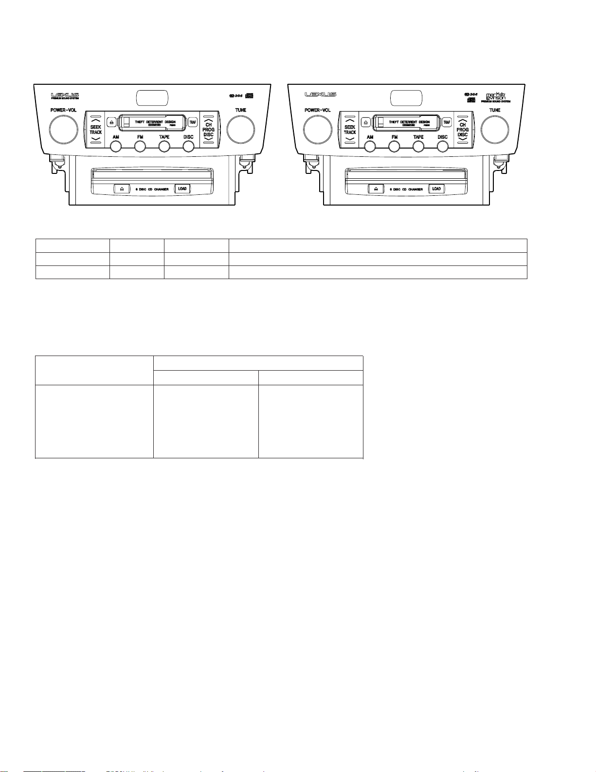
LEXUS LS430 U.S.A., CANADA August 2000 86120-50600 P6810 FX-MG8006ZT/UC
LEXUS LS430 U.S.A., CANADA August 2000 86120-50760 P6810 FX-MG8006ZT-91/UC
LEXUS LS430 U.S.A., CANADA August 2000 86120-50590 P6814 FX-MG8506ZT/UC
LEXUS LS430 U.S.A., CANADA August 2000 86120-50750 P6814 FX-MG8506ZT-91/UC
LS430
Page 2
2
FX-MG8006ZT,MG8006ZT-91,MG8506ZT,MG8506ZT-91
- Dolby noise reduction manufactured under license from Dolby Laboratories Licensing Corporation.
"Dolby" and the double-D symbol are trademarks of Dolby Laboratories Licensing Corporation.
FX-MG8006ZT/UC
- Supplementary model is identical to the original except for the addition of following items.
Description Part No.
FX-MG8006ZT-91/UC FX-MG8506ZT-91/UC
Polyethylene Bag CEG1026 CEG1026
Carton CHA4120 CHA4120
Contain Box CHL4122 CHL4123
Protector(TOP) CHP2319 CHP2319
Protector(BOTTOM) CHP2320 CHP2320
FX-MG8506ZT/UC
ID No.P6810
ID No.P6814
- This service manual should be used together with the following manual(s):
Model No. Order No. Mech. Module Remarks
CX-631 CRT1640 2L Cassette Mech. Module:Mech.Description, Disassembly
CX-890 CRT2376 G1 CD Mech. Module:Circuit Description, Mech.Description, Disassembly
CONTENTS
1. SAFETY INFORMATION ............................................3
2. EXPLODED VIEWS AND PARTS LIST.......................4
3. BLOCK DIAGRAM AND SCHEMATIC DIAGRAM...12
4. PCB CONNECTION DIAGRAM ................................32
5. ELECTRICAL PARTS LIST ........................................54
6. ADJUSTMENT..........................................................60
7. GENERAL INFORMATION .......................................63
7.1 DIAGNOSIS.......................................................63
7.1.1 TEST MODE.............................................63
7.1.2 DIAGNOSIS MODE .................................68
7.1.3 DISASSEMBLY ........................................72
7.1.4 PCB LOCATIONS.....................................77
7.1.5 CONNECTOR FUNCTION DESCRIPTION ..78
7.2 IC........................................................................79
7.3 EXPLANATION..................................................84
7.3.1 SYSTEM BLOCK DIAGRAM ...................84
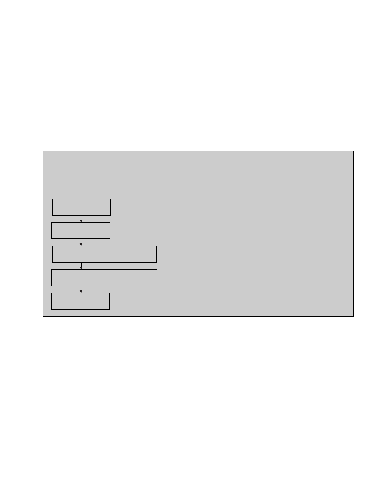
7.3.2 OPERATIONAL FLOW CHART................86
8. OPERATIONS AND SPECIFICATIONS.....................87
Page 3
3
FX-MG8006ZT,MG8006ZT-91,MG8506ZT,MG8506ZT-91
- CD Player Service Precautions
1. For pickup unit(CXX1313) handling, please refer
to"Disassembly"(see page 72).
During replacement, handling precautions shall be
taken to prevent an electrostatic discharge(protection
by a short pin).
2. During disassembly, be sure to turn the power off
since an internal IC might be destroyed when a connector is plugged or unplugged.
3. Please checking the grating after changing the service pickup unit(see page 61).
- When the Repair is Complete
When the repair is complete, make the CD mechanism
ready for transportation
Bup On, Acc OFF
SEEK/TRACK UP+
DISC(CD)+Acc ON
Bup OFF, Acc OFF
Shift completion to the transportation mode.
Disc loading slot illumination : Lighting
Disc loading slot illumination : Blinking
The mode is shifting to the transportation mode.
1. SAFETY INFORMATION
This service manual is intended for qualified service technicians; it is not meant for the casual do-it-yourselfer.
Qualified technicians have the necessary test equipment and tools, and have been trained to properly and safely repair
complex products such as those covered by this manual.
Improperly performed repairs can adversely affect the safety and reliability of the product and may void the warranty.
If you are not qualified to perform the repair of this product properly and safely; you should not risk trying to do so
and refer the repair to a qualified service technician.
Page 4
4
FX-MG8006ZT,MG8006ZT-91,MG8506ZT,MG8506ZT-91
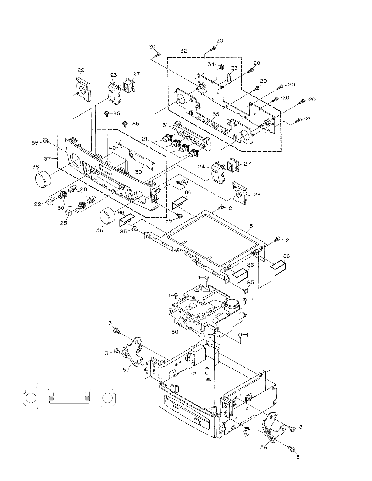
2. EXPLODED VIEWS AND PARTS LIST
2.1 EXTERIOR
35
NOTE:
Please use the gray part shown in figure above cutting off when you exchange the rubber(CNV5881)
for new parts.
Page 5
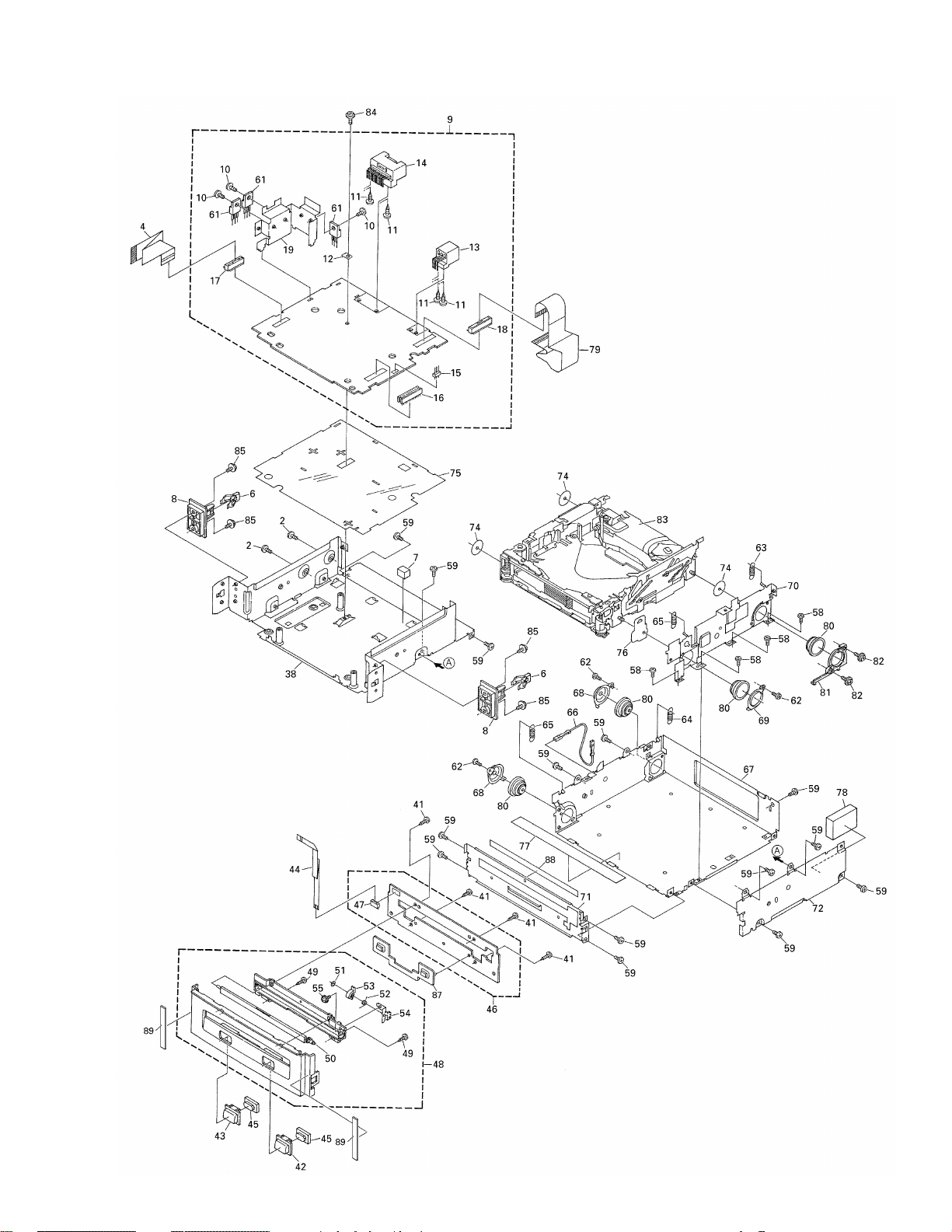
FX-MG8006ZT,MG8006ZT-91,MG8506ZT,MG8506ZT-91
5
Page 6

1 Screw BMZ26P040FMC
2 Screw BMZ26P050FMC
3 Screw BMZ50P080FMC
(FX-MG8006ZT/UC,FX-MG8506ZT/UC)
4 Connector CDE6172
5 Case CNB2542
6 90468-04191 CNC9048
7 Cushion CNM6917
8 Guide CNV6044
9 Main Unit CWM6847
10 Screw BMZ30P060FMC
11 Screw(M3x6) CBA1393
12 Terminal(CN806) CKF1059
13 Connector(CN802) CKM1315
14 Connector(CN801) CKM1322
15 Plug(CN303) CKS-291
16 Connector(CN301) CKS3568
17 Connector(CN804) CKS3751
18 Connector(CN701) CKS3930
19 Holder CNC8163
20 Screw BPZ20P080FMC
21 Button(MODE) CAC5958
22 Button(EJECT) CAC5960
23 Button(SEEK) CAC6356
24 Button(CH) CAC6357
25 Button(TRAF) CAC6431
* 26 Lighting Conductor Unit CXB6916
27 Holder Unit CXB6898
28 Lighting Conductor CNV5683
29 Lighting Conductor Unit CXB6915
30 Holder CNV6039
31 Lighting Conductor Unit CXB6899
32 Keyboard Unit CWM6860
33 Connector(CN902) CKS3751
34 Connector(CN903) CKS4354
35 Rubber CNV5881
36 Knob Unit CXB3551
37 Grille Unit CXB6892
(FX-MG8006ZT/UC,FX-MG8006ZT-91/UC)
Grille Unit CXB6894
(FX-MG8506ZT/UC,FX-MG8506ZT-91/UC)
38 Chassis Unit CXB3549
39 Door(FX-MG8006ZT/UC, CAT2102
FX-MG8006ZT-91/UC)
Door(FX-MG8506ZT/UC) CAT2169
FX-MG8506ZT-91/UC)
40 Spring CBH2427
41 Screw BPZ20P080FMC
42 Button(LOAD) CAC5968
43 Button(EJECT) CAC5969
44 Connector CDE6293
45 Lighting Conductor CNV6638
46 SW Unit CWM6872
47 Connector(CN905) CKS4354
48 Grille Unit CXB6927
49 Screw BPZ20P080FMC
50 Door CAT2151
51 Washer CBF1037
52 Spring CBH2339
53 Gear CNV6116
54 Bracket Unit CXB5254
55 Screw IMS20P030FMC
56 86208-50010 CXB6031
(FX-MG8006ZT/UC,FX-MG8506ZT/UC)
57 86207-50010 CXB6032
(FX-MG8006ZT/UC,FX-MG8506ZT/UC)
58 Screw BMZ20P020FMC
59 Screw BMZ26P030FMC
60
Cassette Mechanism Module EXK3885
61 Transistor(Q809,811,812) 2SB1185
62 Screw(M2x2) CBA1250
63 Spring CBH2361
64 Spring CBH2365
65 Spring Unit CXB6850
66 Connector CDE6302
67 Chassis CNA2131
68 Holder CNC7477
69 Holder CNC7826
70 Holder CNC8160
71 Holder CNC8161
72 Holder CNC8162
73 •••••
74 Sheet CNM5981
75 Insulator CNM7141
76 Sheet CNM6318
77 Insulator CNM6410
78 Cushion CNM6927
79 PCB CNP5399
80 Damper CNV5120
81 Holder CNV5543
82 Screw IMS20P040FMC
83
Mechanism Assy(Service) CXX1430
84 Screw ISS26P050FMC
85 Screw ISS26P060FMC
* 86 Seal CNM5714
87 Rubber CNV6596
88 Spacer CNM7140
89 Spacer CNM7179
FX-MG8006ZT,MG8006ZT-91,MG8506ZT,MG8506ZT-91
- EXTERIOR SECTION PARTS LIST
Mark No. Description Part No.
Mark No. Description Part No.
NOTE:
- Parts marked by "*"are generally unavailable because they are not in our Master Spare Parts List.
- Screws adjacent to ∇ mark on the product are used for disassembly.
6
Page 7
7
FX-MG8006ZT,MG8006ZT-91,MG8506ZT,MG8506ZT-91
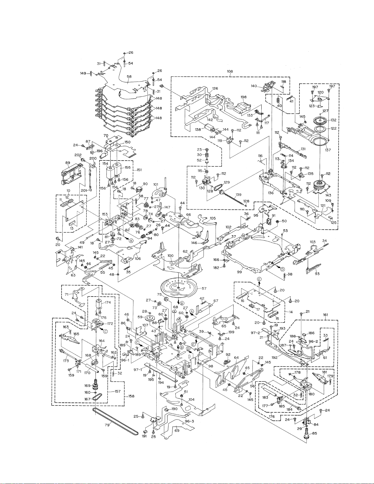
2.2 CD MECHANISM
Page 8

8
FX-MG8006ZT,MG8006ZT-91,MG8506ZT,MG8506ZT-91
1-9 •••••
10 CD Core Unit(Servo Unit) CWX2421
11 Connector(CN101) CKS2764
12 Connector(CN301) CKS3966
13 Connector(CN201) CKS3991
14 CD Core Unit(STS Unit) CWX2422
15 Connector(CN701) CKS3989
16 Connector(CN801) CKS3989
17 Connector(CN802) CKS4054
18 Screw CBA1037
19 Screw CBA1041
20 Screw CBA1076
21 Screw CBA1250
22 Washer CBA1512
23 Screw CBA1452
24 Screw CBA1453
25 Screw CBA1479
26 Washer CBF1037
27 Washer CBF1038
28 Washer CBF1039
29 Washer CBF1064
30 Spring CBH2007
31 Spring CBH2271
32 Spring CBH2274
33 Spring CBH2014
34 Spring CBH2015
35 Spring CBH2016
36 Spring CBH2017
37 Spring CBH2290
38 Spring CBH2366
39 Spring CBH2064
40 Spring CBH2195
41 Spring CBH2196
42 Spring CBH2224
43 Spring CBH2250
44 Screw CBA1082
45 Roller CLA3154
46 Roller CLA3157
47 Roller CLA3159
48 Roller CLA3160
49 Shaft CLA3179
50 Spacer CLA3194
51 Roller CLA3248
52 Bush CLA3353
* 53 Shaft CLA3469
54 Shaft CLA3693
55 Steer CNC7215
56 Steer CNC7216
57 Cam CNC8774
* 58 Holder CNC7235
59 Gear CNC7236
60 Gear CNC8883
61 Lever CNC7243
62 Lever CNC7244
63 Lever CNC7245
64 Lever CXB4944
65 Cover CNC7441
66 Holder Unit CXB4946
67 Lever CNC9088
68 Gear CNC8140
69 Sheet CNM6840
70 PCB CNP5764
71 PCB CNP6010
72 Gear CNR1479
73 Gear CNR1481
74 Gear CNR1495
75 Gear CNR1501
76 Gear CNR1502
77 Gear CNR1540
78 Gear CNR1541
79 Belt CNT1080
80 Worm Gear CNV5046
81 Gear CNV5047
82 Gear CNV5048
83 Gear CNV5049
84 Holder CNV5056
85 Pulley CNV5058
86 Arm CNV5061
87 Spacer CNV5066
88 Arm CNV5189
89 Cover CNV5207
90 Cover CNV5424
91 Cover CNV5425
92 Lever CNV5427
93 Arm CNV5491
94 Gear CNV5519
95 Holder CNV5648
96 Composite PCB CNX3327
97 Composite PCB CNX2989
98 Chassis Unit CXB5940
99 Frame Unit CXB5806
100 Lever Unit CXB6026
101 Arm Unit CXB2704
102 Lever Unit CXB2708
103 Lever Unit CXB2709
- CD MECHANISM SECTION PARTS LIST
Mark No. Description Part No.
Mark No. Description Part No.
Page 9

9
FX-MG8006ZT,MG8006ZT-91,MG8506ZT,MG8506ZT-91
104 Lever Unit CXB4949
105 Arm Unit CXB2712
106 Lever Unit CXB4948
107 Lever Unit CXB2714
108
Carriage Mechanism Unit(G1) CXB4941
109 Screw CBA1041
110 Screw CBA1250
111 Screw CBA1362
112 Screw CBA1471
113 Washer CBF1038
114 Spring CBH2008
115 Spring CBH2009
116 Spring CBH2010
117 Spring CBL1335
118 Roller CLA3913
* 119 Bracket CNC7228
120 Guide Unit CXB4417
121 Cover CNC7628
122 Sheet CNM6414
123 Sheet CNM5378
124 •••••
125 Sheet CNM5827
126 PCB CNP4978
127 Ball CNR1189
128 Bearing CNR1423
129 Belt CNT1079
130 Holder CNV5037
131 Guide CNV5040
132 Clamper CNV5042
133 Rack CNV5111
134 Arm CNV5579
135 Holder CNV5759
* 136 Chassis CXB6025
137 Arm Unit CXB2705
138
Motor Unit(M4 CARRIAGE) CXB3178
139 Screw Unit CXB3179
140 Lever Unit CXB4450
141 Bracket CNC8584
142 Spacer CNM6345
143 Motor(M5 SPINDLE) CXM1120
144 Screw JFZ14P020FZK
145 Washer YE15FUC
146 Arm Unit CXB6052
147 Arm Unit CXB6053
148 Tray Assy CXB4307
149 Spring CBH2269
150 Sheet CNM7109
151 Cam Motor Assy CXB5240
152 •••••
* 153 Bracket Unit CXB5201
* 154
Motor Unit(M1 Cam Gear) CXB3174
* 155 Motor Unit(M3 ELV) CXB3175
156 Screw JFZ20P025FMC
157 Loading Arm L Assy CXB3171
158
Loading Arm L Assy(Service)CXX1415
159 Screw CBA1453
160 Washer CBF1038
161
Loading Arm R Assy(Service)CXX1457
162 Washer CBF1074
163 Spring CBH2136
* 164 Arm CNC7241
* 165 Arm CXB4449
166 Holder CBL1508
167 Belt CNT1079
168 Holder CNV5055
169 Pulley CNV5057
170 Roller CNV6209
171 Guide CNV5125
* 172 Bracket Unit CXB5937
173 Roller Gear Unit CXB3176
* 174 Motor Unit(M2 LOAD) CXB3177
175 Screw JFZ14P020FMC
176 Loading Arm R Assy CXB5839
177 Screw CBA1453
178 Washer CBF1074
179 Spring CBH2136
* 180 Arm CNC7242
* 181 Arm CXB5822
182 Screw JFZ20P014FMC
183 Roller CNV6209
184 Roller Gear Unit CXB3176
185 Guide CNV5126
186
Switch(S885 MAX DETECT) CSN1052
187 LED(D883) CL202IRXTU
188 Photo-transistor(Q881) CPT230SCTD
189 LED(D891,892) CL202IRXTU
190 Switch(S887 CLAMP) CSN1051
191 Switch(S886 ELV HOME) CSN1052
192 Bracket Unit CXB6086
193
Photo-transistor(Q851,852) CPT230SCTD
194 Resistor(R856) RS1/8S911J
195 Resistor(R857) RS1/8S821J
196 Photo-interrupter(Q1) RPI-221
197 Screw CBA1387
198 Pickup Unit(Service)(P8) CXX1313
199 Spring CBL1467
200 Bracket CNC8902
201 Connector CDE6302
202 Screw CBA1015
Mark No. Description Part No.
Mark No. Description Part No.
Page 10
10
FX-MG8006ZT,MG8006ZT-91,MG8506ZT,MG8506ZT-91
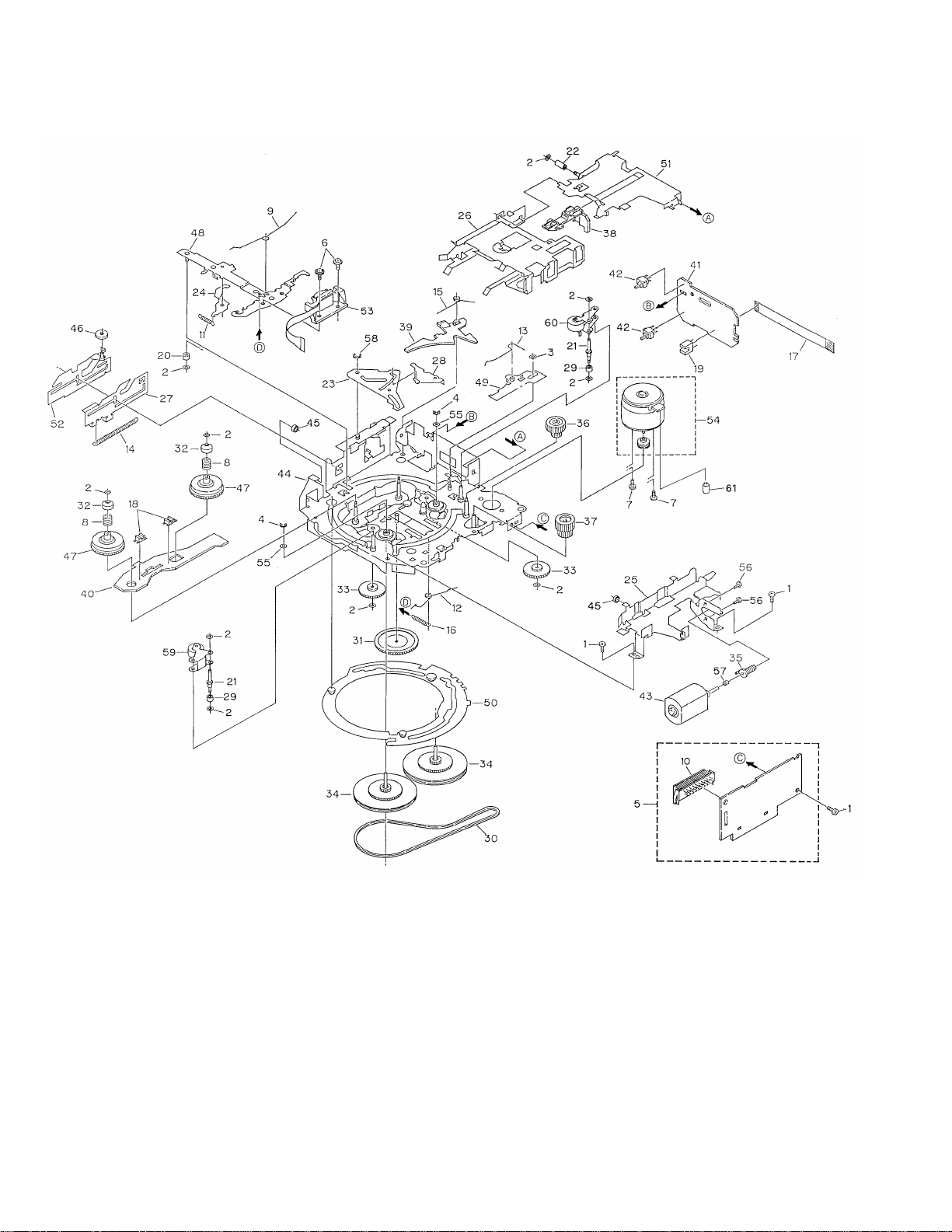
2.3 CASSETTE MECHANISM MODULE
Page 11

11
FX-MG8006ZT,MG8006ZT-91,MG8506ZT,MG8506ZT-91
1 Screw BSZ20P040FMC
2 Washer CBF1037
3 Washer CBF1038
4 Washer CBG1003
5 Deck Unit EWM1027
6 Screw(M2x5) EBA1028
7 Screw(M2x2.5) EBA1037
8 Spring EBH1531
9 Spring EBH1589
10 Connector(CN251) CKS3540
11 Spring EBH1515
12 Spring EBH1587
13 Spring EBH1517
14 Spring EBH1518
15 Spring EBH1519
16 Spring EBH1537
17 Cord EDD1027
18 Photo-interrupter
(EGN2,3) EGN1006
19 Photo-interrupter(EGN1) EGN1005
20 Roller ENR1031
21 Shaft ELA1362
22 Roller ELA1348
23 Arm ENC1490
24 Arm ENC1397
25 Guide ENC1519
26 Holder ENC1516
27 Lever ENC1448
28 Arm ENC1488
29 Roller ENR1023
30 Belt ENT1027
31 Gear ENV1347
32 Collar ENV1508
33 Gear ENV1350
34 Flywheel ENV1500
35 Worm Gear ENV1439
36 Worm Wheel ENV1440
37 Gear ENR1037
38 Lever ENV1533
39 Arm ENV1525
40 Gathering PCB ENX1037
41 Gathering PCB ENX1060
42 Switch(S1)(S2) ESG1004
43 Motor Unit(M2)(SUB) EXA1382
44 Chassis Unit EXA1559
45 Tube ENM1039
46 Roller ENR1027
47 Reel Unit EXA1560
48 Head Base Unit EXA1434
49 Lever Unit EXA1578
50 Gear Unit EXA1545
51 Frame Unit EXA1476
52 Lever Unit EXA1439
53 Head Assy(HD1) EXA1594
54 Motor Unit(M1)(MAIN) EXA1499
55 Washer HBF-179
56 Screw JGZ20P025FNI
57 Spring EBH1545
58 Washer YE20FUC
59 Pinch Roller Unit EXA1533
60 Pinch Roller Unit EXA1532
61 Capacitor(C1) CEAL4R7M35
Mark No. Description Part No. Mark No. Description Part No.
- CASSETTE MECHANISM MODULE SECTION PARTS LIST
Page 12
12
A
1
234
B
C
D
12
34
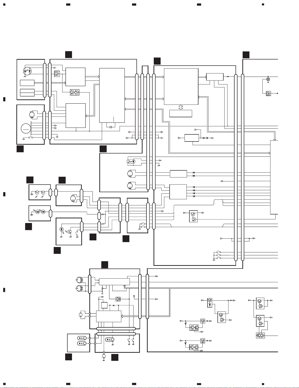
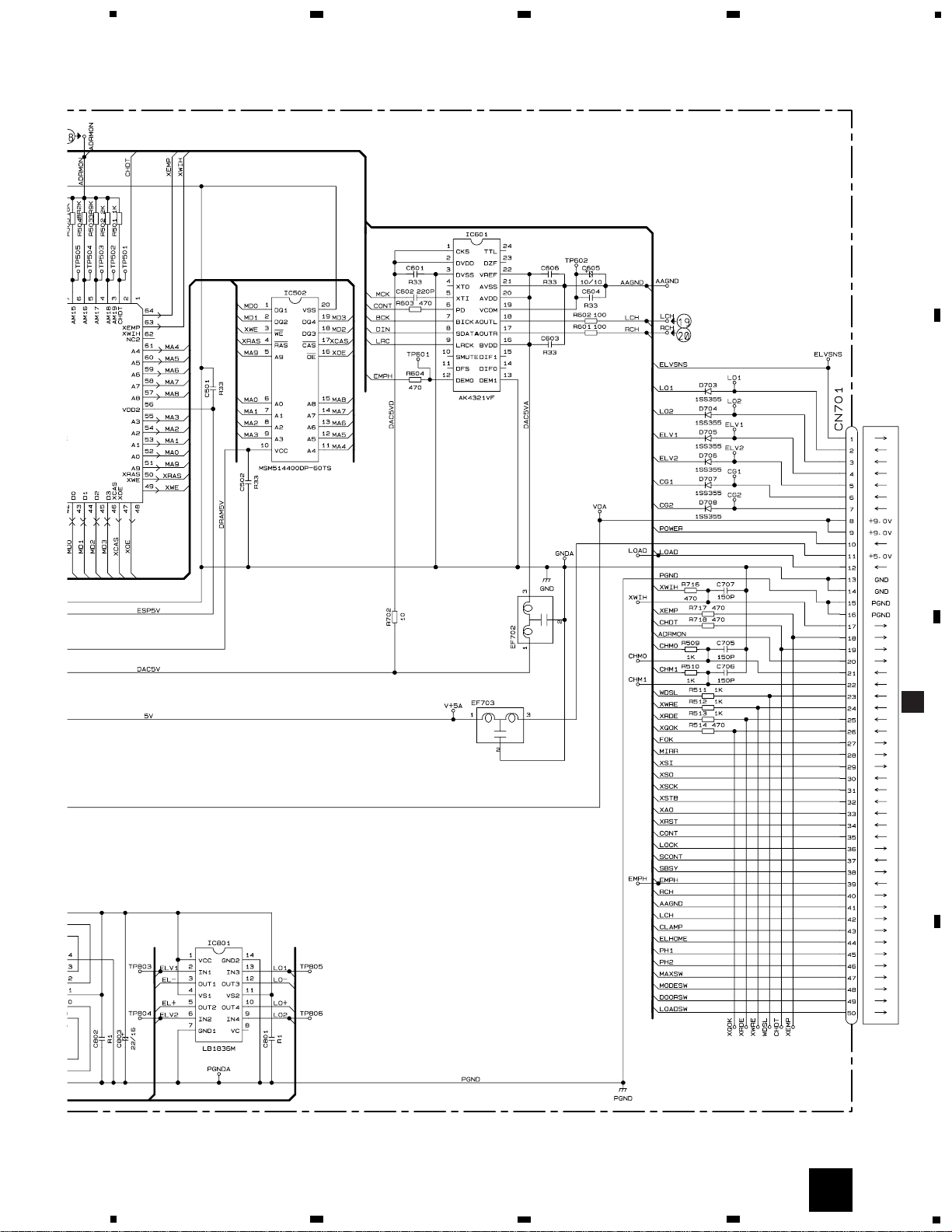
3. BLOCK DIAGRAM AND SCHEMATIC DIAGRAM
3.1 BLOCK DIAGRAM
FX-MG8006ZT,MG8006ZT-91,MG8506ZT,MG8506ZT-91
8.5V
BU
60
59
58
57
78
77
76
ELV1
ELV2
LO1
LO2
PH2
PH1
PH3
LOAD
ELHOME
CLAMP
55
6
CG1
CG2
62
61
POWER
26
Q702
Q301
CD MUTE
DOORSW
LOADSW
MODESW
79
ELVSNS
TAPEB
TL
BUS
LOAD
PH1
PH2
PH3
LO2
LO1
ELV2
ELV1
CG2
CG1
elvsns
POWER
CONT
EMPH
VD
Lch
3
1
2
8
7
39
6
5
4
48
49
46
47
44
45
50
41
16
12
42
VD
CD9V
43
9
CN701
BUCD9V
CN251
CN301
CN252
CN253
IC251
HA12216F
TAPE EQUALIZER
MECHANISM DRIVER
IC351
PA2020A
Q271
B.U
B.U
M
SUB
MOTOR
M
MAIN
MOTOR
10
+B
TAPE-L
MTL
MTL
VR301
VREF
6
22
14
17
2
51
53
17
7
18
19
5
2
NR
Q351
Q352
1
9
8
STBY
LOAD
LOAD
SWITCH
70µs
SWITCH
MODE
SENSE
FWD
SENSE
REV
SENSE
1
4
5
4
3
20
4
3
20
FWD
LcH
REV
LcH
23
8
1
64
23
8
1
64
Q854
Q809
CD9V
AUDIO8.5V
BU
VDD
ILL8V
BU
BU
BU8.5V
Q852
Q817 Q816
Q808
Q856
Q804
VDD REGULATOR ILL8V REGULATOR
SW5V
Q811
Q813
Q812
Q814
40
CD5V
EREF
75
VDCONT
SW5V
DECK UNIT
PCB UNIT
REEL PCB
MAIN UNIT
PICKUP UNIT(SERVICE)
MOTOR PCB(B)
MOTOR PCB(A)
CD CORE UNIT(SERVO UNIT)
PCB UNIT(D)
PCB UNIT(A)
PCB UNIT(C)
PCB UNIT(E)
PCB UNIT(B)
LOAD MOTOR PCB
CD CORE UNIT(STS UNIT)
HOLOGRAM
UNIT
FOCUS ACT
TRACKING ACT
MD
LD+
LD-
LD
MD
FO+
TO+
16
17
V5
Q101
Q102
PD
LD
CN101
IC 101
UPC2572GS
RF AMP
IC 201
UPD63702AGF
DIGITAL SERVO
PROCESSOR
DIGITAL SIGNAL
PROCESSOR
µ-COMPUTER
INTERFACE
35
69
EFM
CD 4CH DRIVER
IC 301
BA5986FM
14
11
16
15
22
BVD
V5
MUTE
9
MD/SD/TD/FD
74
10
11
VR2
XTAL
XTAL
X201
5V
VD
CONT
CN201
CN801
5V
VD
CN301
WDCK
RFCK
RAOV
LRCK
SCKO
DOUT
MCK
IC 501
CXD2511R
SHOCKPROOF
CONTROLLER
BCK
DATA
LRCK
XTLI
39
512
IC 601
AK4321VF
8fs DF D/A LPF
CN701
6
18
DEMO
PD
IC 502
MSM514400DP-60TS
4M DRAM
VD
VD
LCH
WDSL/CHMO/CHMI
XWRE/XRDE/XQOK
XWIH/XEMP/ADRMON/CHDT
V+5V
IC 701
BA05SFP
5V REGULATOR
VM
VD
POWER
CONT
EMPH
4
2
1
XAO/XSTB/XSO/XSI/XSCK/XRST/SCONT
ELVSNS
LOADSW
DOORSW
MODESW
S801
S802
S803
MOTOR DRIVER
IC 802
LB1836M
2
6
3
5
ELVSNS
MOTOR DRIVER
LB1836M
IC 801
2
6
13
9
5
3
12
10
CG1
CG2
CGCG+
ELEL+
ELV1
ELV2
LO1
LO2
MAXSW
PH2
PH1
PVD
LOLO+
PVD
PVD
Q801
VD
Q802
LOAD
ELHOME
CLAMP
CLAMP
ELHOME
CN802
M
BCL
SPINDLE
MOTOR
CARRIAGE
MOTOR
HOME
SWITCH
EC
VM
VCC
ST/SR
GND
HOME
M
LOADING
MOTOR
M
CAMGEAR
MOTOR
M
ELEVATION
MOTOR
Q851
Q852
D891
D892
PH1
PVD
Q881
D883
PH2
S883
MAX DETECT
SWITCH
PH1
PVD
PH1
PH2
MAXSW
LD MOTOR-
LD MOTOR+
MAXSW
PH2
PH1
PVD
ELV HOME
S886
S887
CLAMP
ELEVATION
SENSE
V+5V
5
14
15
4
3
1
2
3
4
8
5
6
7
10
11
1
1
1
1
2
3
4
1
2
4
1
2
1
1
2
3
5
6
3
4
2
1
5
6
3
4
2
1
5
7
3
4
2
1
7
5
9
8
10
11
10
2
11
1
19
28
29
30
19
28
29
30
45
44
46
42
8
9
35
39
10
1
50
49
48
6
7
11
4
5
2
3
47
46
45
12
44
43
36
35
37
32
33
39
41
41
43
48
50
LOAD
E
F
G
I
19
19
28
28
29
29
30
30
O
P
N
H
I
J
L
K
M
D F
E
G
A
Page 13
13
FX-MG8006ZT,MG8006ZT-91,MG8506ZT,MG8506ZT-91
5
6
7
8
5
6
7
8
A
B
C
D
CN802
L+
L-
MUTE
ILL+
ACC
ILL-
TX+
TX-
TXS+
TXS-
+B
BU
CN801
IC701
PD5575B
SYSTEM CONTROLLER
IC601
PD5556B
60
59
58
57
78
77
76
ELV1
ELV2
LO1
LO2
PH2
PH1
PH3
LOAD
modesw
55
6
5
CG1
CG2
62
61
POWER
26
27
53
Q702
Q301
CD MUTE
56
X701
6.290MHz
X601
10.00MHz
28
29
EMPH
CONT
cdmute
50
TAPEMUTE
MUTE
47
51
sysmute
45
swvdd
XIN
XOUT
15
13
XIN
XOUT
2
17
18
DCLOSE
40
79
loadsw
doorsw
clamp
elhome
elvsns
Q307
TAPE MUTE
SYS MUTE
Q603
Q602 Q309
IC301
NJM2068MD
MIXING
HARD MUTE
SW5V
AVC-LAN BUS DRIVER
RESET
21
IC302
NJM2068MD
21
IC602
HA12187FP
IC603
S-80730ANDT
16
12
IC303
NJM2068MD
21
IC305
TC74HC4066AF
ANALOG SW
43
12
Q303
Q833 Q831
Q305
Q601
EJ EJ
BU
SW5V
BU
MUTE
Q801
ISENS
Q805
BSENS
Q806
ASENS
Q807
ILL-
Q825
ilsens
23
bsens
20
asens
19
25
8
ILL-
94
TX
30
RX1
29
RX2
21
IPPW
22
reset
12
mode
54
ENC1+
55
ENC1-
56
power
88
ENC2+
87
ENC2-
86
illpow
52
CDILL
dssill
49
53
cdej18dload
73
ILL
4
csej
75
VDD
S924
DCLOSE
S923
LOAD
S922
CD EJECT
CN903
CN905
CN902
CN804
71
8910
410
321
21
20
KEY
MATRIX
VR901
TUNE
S901
TAPE
EJECT
25
16
MODE MODE
5
36
ENC1P ENC1P
3
38
ENC1M ENC1M
1
40
ENC2P
28
13
PWR PWR
29
12
ENC2M
31
10
VILM2 ILL2
34
7
VCILL CILL
24
17
VILL1 ILL1
33
8
CDEJ CDEJ
22
19
DLOAD DLOAD
18
23
DCLOSE DCLOSE
Q824 Q830
Q829
Q828 Q827
Q826
Q823
Q822
ILL8V
BU
BU
16
EREF
75
UNBAL → BAL
VR902
POWER-VOL
ENC2P
ENC2M
CD CONTROLLER
C
RESET
25
VDCONT
13
VDCONT
RESET
SW UNIT
KEYBOARD UNIT
B
Page 14
14
FX-MG8006ZT,MG8006ZT-91,MG8506ZT,MG8506ZT-91
A
1
234
B
C
D
12
34
A
MAIN UNIT
KEYBOARD UNIT
C
G
CD CORE UNIT(STS UNIT)
N
CN251
MODE
CDEJ
MIXING AMP
CD MUTE
TAPE MUTE
ILL2 SELECTOR
CD ILL SELECTOR
CD CONTROLLER
CD 0dB 1kHz : +2.1dBs
TAPE 250nwb/m 315Hz : -7.2dBs
TAPECD: -4.8dBs
: +2.2dBs
A
A-aA-a A-b A-b
A-a
A-b
A-b
A-a
Large size
SCH diagram
Guide page
Detailed page
A-a
3.2 OVERALL CONNECTION DIAGRAM(GUIDE PAGE)
Note: When ordering service parts, be sure to refer to “EXPLODED VIEWS AND PARTS LIST” or “ELECTRICAL
PARTS LIST”.
Page 15
FX-MG8006ZT,MG8006ZT-91,MG8506ZT,MG8506ZT-91
5
6
7
8
A
B
C
D
5
6
7
8
15
Decimal points for resistor
and capacitor fixed values
are expressed as :
2.2 2R2
0.022 R022
←
←
The > mark found on some component parts indicates
the importance of the safety factor of the part.
Therefore, when replacing, be sure to use parts of
identical designation.
Symbol indicates a resistor.
No differentiation is made between chip resistors and
discrete resistors.
NOTE :
Symbol indicates a capacitor.
No differentiation is made between chip capacitors and
discrete capacitors.
PWR
ENC2P
ENC2M
DLOAD
UNBALANCE TO BALANCE CONVERTER
ANALOG SWITCH
HARD MUTE
BUS DRIVER
VDD 5V REGULATOR
LPF
AUDIO 8.5V REGULATOR
CD 9V REGULATOR
ILLUMINATION 8V REGULATOR
ILL1 SELECTOR
SYSTEM CONTROLLER
TAPE : +1.2dBs
RESET
A
A-b
Page 16
16
FX-MG8006ZT,MG8006ZT-91,MG8506ZT,MG8506ZT-91
A
MAIN UNIT
NIT(STS UNIT)
N
CN251
MODE
MIXING AMP
CD MUTE
TAPE MUTE
CD 0dB 1kHz : +2.1dBs
TAPE 250nwb/m 315Hz : -7.2dBs
TAPE
CD
: -4.8dBs
: +2.2dBs
A
1
234
B
C
D
1
2
34
A-a
A-b
A-a
1
2
3
4
5
Page 17
17
FX-MG8006ZT,MG8006ZT-91,MG8506ZT,MG8506ZT-91
KEYBOARD UNIT
C
G
CD CORE UNIT(S
CDEJ
ILL1 SEILL2 SELECTOR
CD ILL SELECTOR
CD CONTROLLER
5
6
7
8
A
B
C
D
5
6
7
8
A-a
A-b
A-a
7
6
8
Page 18
18
FX-MG8006ZT,MG8006ZT-91,MG8506ZT,MG8506ZT-91
Decimal points for resistor
and capacitor fixed values
are expressed as :
2.2 2R2
0.022 R022
←
←
The > mark found on some component parts indicates
the importance of the safety factor of the part.
Therefore, when replacing, be sure to use parts of
identical designation.
Symbol indicates a resistor.
No differentiation is made between chip resistors and
discrete resistors.
NOTE :
Symbol indicates a capacitor.
No differentiation is made between chip capacitors and
discrete capacitors.
DLOAD
UNBALANCE TO BALANCE CONVERTER
ANALOG SWITCH
HARD MUTE
BUS DRIVER
VDD 5V REGULATOR
SYSTEM CONTROLLER
TAPE : +1.2dBs
A
1
234
B
C
D
12
34
A-a
A-b
A-b
1
2
3
4
5
Page 19
19
FX-MG8006ZT,MG8006ZT-91,MG8506ZT,MG8506ZT-91
PWR
ENC2P
ENC2M
DLOAD
LPF
AUDIO 8.5V REGULATOR
CD 9V REGULATOR
ILLUMINATION 8V REGULATOR
ILL1 SELECTOR
RESET
5
6
7
8
A
B
C
D
5
6
7
8
A-a
A-b
A-b
6
7
8
Page 20
20
FX-MG8006ZT,MG8006ZT-91,MG8506ZT,MG8506ZT-91
A
1
234
B
C
D
12
34
1
324
5
KEYBOARD UNIT
B
C
SW UNIT
1
324
5
TAPE EJECT
TRAF
3.3 SW UNIT, KEYBOARD UNIT
B
C
Page 21
21
FX-MG8006ZT,MG8006ZT-91,MG8506ZT,MG8506ZT-91
5
6
7
8
A
B
C
D
5
6
7
8
CN804
MAIN UNIT
A
C
B
Page 22
22
FX-MG8006ZT,MG8006ZT-91,MG8506ZT,MG8506ZT-91
A
1
234
B
C
D
12
34
M5 SPINDLE
CXM1120
DISC INSERT DETECT
M4 CARRIAGE
CXB3178
D
MOTOR PCB(B)
PICKUP UNIT
(SERVICE)(P8)
RF AMP/
AUTO POWER
CONTROL
CD DRIVER
E
CD CORE UNIT(SERVO UNIT)
3.4 CD CORE UNIT(SERVO UNIT)
D
E
Page 23
23
FX-MG8006ZT,MG8006ZT-91,MG8506ZT,MG8506ZT-91
5
6
7
8
A
B
C
D
5
6
7
8
FOCUS/TRACKING
CARRIAGE/SPINDLE
DIGITAL SERVO
DIGITAL SIGNAL PROCESSOR
D/A CONVERTER
F
E
Page 24
24
FX-MG8006ZT,MG8006ZT-91,MG8506ZT,MG8506ZT-91
A
1
234
B
C
D
12
34
E
CD CORE UNIT
(SERVO UNIT)
M1 : CXB6929
Q1 : RPI-221
M3 : CXB3175
F
MOTOR PCB
(A)
ELV SENSE
SURE TRACK
MEMORY CONTROLLER
G
CD CORE UNIT(STS UNIT)
MOTOR DRIVER
H
+5V REGULATOR
3.5 CD CORE UNIT(STS UNIT)
F
G
Page 25
25
FX-MG8006ZT,MG8006ZT-91,MG8506ZT,MG8506ZT-91
5
6
7
8
A
B
C
D
5
6
7
8
D/A CONVERTER
4M DRAM
?
CN???
MOTOR DRIVER
G
A
CN701
Page 26
26
FX-MG8006ZT,MG8006ZT-91,MG8506ZT,MG8506ZT-91
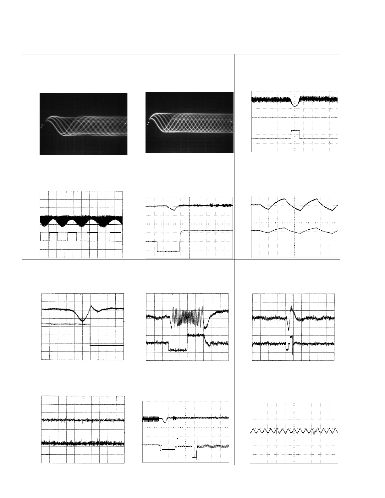
1 RFO 0.5V/div. 0.2µs/div.
Normal mode: play
1 CH1: RFO 1V/div.
2 CH2: MIRR 5V/div.
Test mode: Tracking open
0.5ms/div.
1 CH1: RFO 1V/div.
2 CH2: MIRR 5V/div.
Normal mode: The defect part
passes 500µs/div.
0.5ms/div.
3 CH1: FIN 0.5V/div.
4 CH2: FOP 2V/div.
Test mode: No disc, Focus close
0.2s/div.
3 CH1: FIN 0.5V/div.
5 CH2: FOK 2V/div.
Normal mode: Focus close
0.2s/div.
6 CH1: FEY 0.5V/div.
7 CH2: XSI 2V/div.
Normal mode: Focus close
1ms/div.
8 CH1: TEY 0.5V/div.
9 CH2: TIN 0.5V/div.
Test mode: 32 tracks jump (FWD)
0.5ms/div.
8 CH1: TEY 0.5V/div.
9 CH2: TIN 0.5V/div.
Test mode: Single jump (FWD)
0.5ms/div.
6 CH1: FEY 0.1V/div.
3 CH2: FIN 0.2V/div.
Normal mode: Play
20ms/div.
3 CH1: FIN 0.5V/div.
0 CH2: SIN 1V/div.
Normal mode: Focus close
0.5s/div.
GND
→
GND
→
GND
→
GND
→
- Waveforms
0 SIN 0.5V/div. 0.1s/div.
Normal mode: Play
REFOUT
→
REFOUT
→
REFOUT
→
REFOUT
→
REFOUT
→
REFOUT
→
REFOUT
→
REFOUT
→
REFOUT
→
REFOUT
→
REFOUT
→
REFOUT
→
REFOUT
→
REFOUT
→
REFOUT
→
REFOUT
→
1 RFO 0.5V/div. 0.5µs/div.
Test mode
REFOUT
→
REFOUT
→
REFOUT
→
Note:1. The encircled numbers denote measuring pointes in the circuit diagram.
2. Reference voltage
REFOUT:2.5V
Page 27
27
FX-MG8006ZT,MG8006ZT-91,MG8506ZT,MG8506ZT-91
3 CH1: FIN 1V/div.
$ CH2: HOLD 5V/div.
Normal mode:
The defect part passes 800µm
8 CH1: TEY 0.5V/div.
6 CH2: FEY 0.1V/div.
Normal mode: AGC after focus close
8 CH1: TEY 0.5V/div.
! CH2: SD 0.5V/div.
5ms/div.
0 SIN 1V/div. 10ms/div.
Long Search
8 CH1: TEY 1V/div.
# CH2: TEC 1V/div.
Test mode: Focus close
Tracking open
2ms/div.
6 CH1: FEY 0.2V/div.
3 CH2: FIN 0.5V/div.
Normal mode: During
AGC
1ms/div.
@ EFM 1V/div. 2µs/div.
Play
0.2s/div.
% Dout 2V/div. 5µs/div.
Play
^ LRCK 2V/div. 10µs/div. * ADRMON 1V/div. 1s/div.
Normal mode: Starting play
GND
→
REFOUT
→
REFOUT
→
REFOUT
→
REFOUT
→
REFOUT
→
REFOUT
→
REFOUT
→
REFOUT
→
REFOUT
→
REFOUT
→
REFOUT
→
REFOUT
→
REFOUT
→
REFOUT
→
1 CH1: RFO 1V/div.
$ CH2: HOLD 5V/div.
Normal mode:
The defect part passes 800µm
500µs/div.
REFOUT
→
REFOUT
→
8 CH1: TEY 0.2V/div.
9 CH2: TIN 0.5V/div.
Normal mode: During
AGC
1ms/div.
REFOUT
→
REFOUT
→
GND
→
GND
→
500µs/div.
Page 28

28
FX-MG8006ZT,MG8006ZT-91,MG8506ZT,MG8506ZT-91
8 CH1: TEY 0.5V/div.
9 CH2: TIN 0.5V/div.
Test mode: 100 tracks jump(FWD)
8 CH1: TEY 0.5V/div.
9 CH2: TIN 0.5V/div.
Normal mode: Play
10ms/div.
5ms/div.
REFOUT
→
REFOUT
→
& SCKO 2V/div. 500ns/div.
Play
REFOUT
→
) CH1: RCH 2V/div.
( CH2: LCH 2V/div.
Normal mode: PLAY (0dB,1kHz)
200µs/div.
AAGND
→
AAGND
→
REFOUT
→
REFOUT
→
Page 29

29
FX-MG8006ZT,MG8006ZT-91,MG8506ZT,MG8506ZT-91
1
2
3
4
A
B
C
D
1
2
3
4
H
I
J
L
M
K
CXB3177
G
CN802
MAX DETECT SWITCH
PCB UNIT(A)
PCB UNIT(C)
PCB UNIT(E)
PCB UNIT(B)
PCB UNIT(D)
LOAD MOTOR PCB
CPT230SCTD
CPT230SCTD
S886:CSN1052
S887:CSN1051
3.6 PCB UNIT(A,B,C,D,E), LOAD MOTOR PCB
M
J
I
H
K
L
Page 30

30
FX-MG8006ZT,MG8006ZT-91,MG8506ZT,MG8506ZT-91
A
1
234
B
C
D
12
34
DECK UNIT
B/C
HA12216F
11
12
13
14
15
16
17
18
19
20
40
39
38
37
36
35
34
33
32
31
30
292827
26
252423
22
21
1
234
5
678
9
10
R256
180
R291
0R0
C271
1/50
R283 0R0
R284 0R0
R282 0R0
C253 390P
C254 390P
C252 390P
C251 390P
R281 0R0
R255
180
C256
R01
R258
18K
R402
3R3K
R403 910
R275
47K
R293
0R0
C272
R1
R285 0R0
HD1
HEAD ASSY
EXA1594
TEST TAPE
NCT-150
(400Hz, 200nWb/m)
RL
RR
FR
FL
C302
R1
VR302
33K(B)
-8.24dBs(300mV)±1dB
Fwd-R
Fwd-L
Rev-R
Rev-L
NFI(L)
RIN(L)
RIP
FIN(L)
GND
GND
FIN(R)
VREF
RIN(R)
NFI(R)
M-OUT(R)
EQOUT(R)
TAI(R)
BIAS
RAI(R)
PBOUT(R)
DET(L)
MUTE
MSGV(R)
MAOUT
MSI
MSDET
MSGV
F/R
120/70
NR
MOUT(L)
EQOUT(L)
TAI(L)
NC
RAI(L)
PBOUT(L)
NC
DET(L)
MSGV(S)
CN252
CN251
DOLBY B NR
IC251
VR301
33K(B)
C310
R1
C309
R1
R321
0R0
VCC
CCP1280
CCP1280
NC
MSOUT
NC
NC
R260
13K
R262
270K
C401
4700P
R401
12K
R276
100K
C402
R33
C404
R01
C403
R022
R288
0R0
R274
0R0
R289
0R0
R273
0R0
R272
0R0
R404
270K
C405
R033
R278
100K
Q271
2SC4116
R292
0R0
R271
18K
C301
R1
R294
0R0
R259
13K
C255
R01
R257
18K
R261
270K
N
N
CN301
A
3.7 CASSETTE MECHANISM MODULE
N
Page 31

31
FX-MG8006ZT,MG8006ZT-91,MG8506ZT,MG8506ZT-91
5
6
7
8
A
B
C
D
5
6
7
8
SWITCHES:
PCB UNIT
S1:LOAD SWITCH..........EJECT-PLAY
S2:70µs SWITCH...............ON-OFF
The underlined indicates the switch position.
R275
47K
R351 1K
R352 1K
R353 1K
R354 1K
R373 0R0
R355
270K
C352
3900P
R362
180
C351 R22
C354 R01
R374 0R0
C355
R1
D351
1SS355
M1 MOTOR UNIT
(MAIN MOTOR)
EXA1499
M2
MOTOR UNIT
(SUB MOTOR)
EXA1382
RS3
RS2
RS1
SC2
SC1
TAB
MC
CE
VCC2
NC
VCC
MCS
RRS
FRS
RSB
C
TAB
MS2
NC
NC
MM
SM1
RRS
GND
FRS
mtl
RSB
load
CN253
CN254
MECHANISM
DRIVER
IC351 PA2020A
R375 0R0
R404
270K
C405
R033
R277
220K
R278
100K
116
PCB UNIT
REEL PCB
S1 LOAD
ESG1004
S2
ESG1004
70µs
MODE
SENSE
EGN1
EGN1005
EGN2
EGN1006
FWD END
SENSE
EGN3
EGN1006
REV END
SENSE
7
7
8
NM
MCS
R357
4R7K
R358
10K
C353
R01
R359
10K
C356
R01
R360
1K
R361
6R2K
R356
2K
Q351
2SB1260
Q352
2SC4102
RES
NES
8
L1
O
P
P
N
O
Page 32

32
FX-MG8006ZT,MG8006ZT-91,MG8506ZT,MG8506ZT-91
A
1
234
B
C
D
12
34
A
A
MAIN UNIT
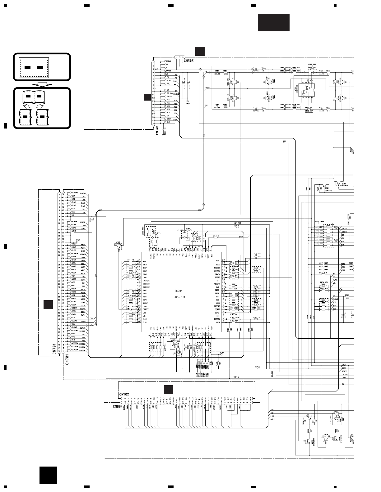
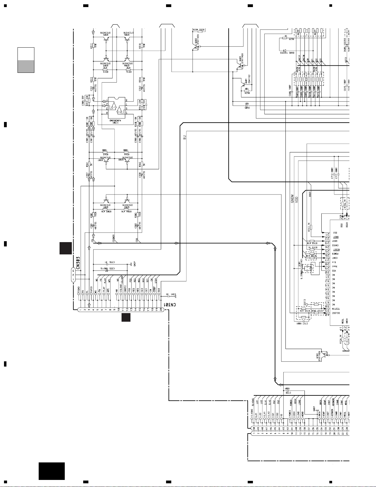
4. PCB CONNECTION DIAGRAM
4.1 MAIN UNIT
Capacitor
Connector
P.C.Board
Chip Part
SIDE A
SIDE B
NOTE FOR PCB DIAGRAMS
1. The parts mounted on this PCB
include all necessary parts for
several destination.
For further information for
respective destinations, be sure
to check with the schematic
diagram.
2. Viewpoint of PCB diagrams
C
CN902
Page 33

33
FX-MG8006ZT,MG8006ZT-91,MG8506ZT,MG8506ZT-91
FRONT
5
6
7
8
A
B
C
D
5
6
7
8
A
SIDE A
CN251
G
CN701
N
Page 34

34
FX-MG8006ZT,MG8006ZT-91,MG8506ZT,MG8506ZT-91
FRONT
A
1
234
B
C
D
12
34
A
A
MAIN UNIT
Page 35

35
FX-MG8006ZT,MG8006ZT-91,MG8506ZT,MG8506ZT-91
5
6
7
8
A
B
C
D
5
6
7
8
A
SIDE B
Page 36

36
FX-MG8006ZT,MG8006ZT-91,MG8506ZT,MG8506ZT-91
DCLOSE
A
1
234
B
C
D
12
34
4.2 SW UNIT
B
SW UNIT
B
C
CN903
SIDE A
LOAD
CD EJECT
Page 37

37
FX-MG8006ZT,MG8006ZT-91,MG8506ZT,MG8506ZT-91
1
2
3
4
A
B
C
D
1
2
3
4
B
B
SW UNIT
SIDE B
Page 38

38
FX-MG8006ZT,MG8006ZT-91,MG8506ZT,MG8506ZT-91
A
1
234
B
C
D
12
34
12
3
45
12
3
45
4.3 KEYBOARD UNIT
C
KEYBOARD UNIT
C
SIDE A
POWER-VOL
TUNE
AM
FM
TAPE
DISC
TRAFTAPE EJECT
SEEK
TRACK
CH
PROG
DISC
Page 39

39
FX-MG8006ZT,MG8006ZT-91,MG8506ZT,MG8506ZT-91
1
2
3
4
A
B
C
D
1
2
3
4
C
SIDE B
KEYBOARD UNIT
A
CN804
B
CN905
C
Page 40

40
FX-MG8006ZT,MG8006ZT-91,MG8506ZT,MG8506ZT-91
A
1
234
B
C
D
12
34
4.4 CD CORE UNIT(SERVO UNIT)
F
E
REFOUT
PICKUP UNIT
(SERVICE)
D
F
CD CORE UNIT(SERVO UNIT)
E
SIDE A
E
Page 41

41
FX-MG8006ZT,MG8006ZT-91,MG8506ZT,MG8506ZT-91
1
2
3
4
A
B
C
D
1
2
3
4
CD CORE UNIT(SERVO UNIT)
E
SIDE B
E
Page 42

42
FX-MG8006ZT,MG8006ZT-91,MG8506ZT,MG8506ZT-91
A
1
234
B
C
D
12
34
E
E
MODE
DOOR
?
F
4.5 CD CORE UNIT(STS UNIT)
CD CORE UNIT(STS UNIT)
G
A
CN701
SIDE A
G
H
F
Page 43

43
FX-MG8006ZT,MG8006ZT-91,MG8506ZT,MG8506ZT-91
1
2
3
4
A
B
C
D
1
2
3
4
CD CORE UNIT(STS UNIT)
G
SIDE B
G
Page 44

44
FX-MG8006ZT,MG8006ZT-91,MG8506ZT,MG8506ZT-91
A
1
234
B
C
D
12
34
4.6 MOTOR PCB(A)
Q1
ELV SENSE
M
M1
CAM GEAR
M
M3
ELV
1
30
D
CN201
E
MOTOR PCB(A)
F
F
SIDE A
Page 45

45
FX-MG8006ZT,MG8006ZT-91,MG8506ZT,MG8506ZT-91
1
2
3
4
A
B
C
D
1
2
3
4
1
41
G
CN801
G
MOTOR PCB(A)
F
F
SIDE B
Page 46

46
FX-MG8006ZT,MG8006ZT-91,MG8506ZT,MG8506ZT-91
A
1
234
B
C
D
12
34
4.7 MOTOR PCB(B)
SPINDLE MOTOR
M5
MOTOR PCB(B)
D
D
Page 47

47
FX-MG8006ZT,MG8006ZT-91,MG8506ZT,MG8506ZT-91
5
6
7
8
A
B
C
D
5
6
7
8
M
M4
CARRIAGE
1
12
E
CN301
D
Page 48

48
FX-MG8006ZT,MG8006ZT-91,MG8506ZT,MG8506ZT-91
A
1
234
B
C
D
12
34
S887
CLAMP
1
1
7
S886
ELV HOME
G
CN802
I
11
4.8 PCB UNIT(B)
PCB UNIT(B)
H
4.9 PCB UNIT(D)
PCB UNIT(D)
M
M
H
Page 49

49
FX-MG8006ZT,MG8006ZT-91,MG8506ZT,MG8506ZT-91
1
2
3
4
A
B
C
D
1
2
3
4
4
1
D883
S885
MAX DETECT
Q881
I
4.10 PCB UNIT(C)
PCB UNIT(C)
J
J
Page 50

50
FX-MG8006ZT,MG8006ZT-91,MG8506ZT,MG8506ZT-91
A
1
234
B
C
D
12
34
M
M2
LOAD
1
1
4
2
I
M
4.11 LOAD MOTOR PCB
4.12 PCB UNIT(A)
D891D892
1
2
I
LOAD MOTOR PCB
K
PCB UNIT(A)
L
K
L
Page 51

51
FX-MG8006ZT,MG8006ZT-91,MG8506ZT,MG8506ZT-91
1
2
3
4
A
B
C
D
1
2
3
4
4.13 PCB UNIT(E)
PCB UNIT(E)
I
PCB UNIT(E)
I
SIDE A SIDE B
I
Page 52

52
FX-MG8006ZT,MG8006ZT-91,MG8506ZT,MG8506ZT-91
A
1
234
B
C
D
12
34
IC,Q ADJ
VR302
IC351
IC251
Q351
Q352
VR301
HEAD
ASSY
M1
M2
CN253
CN254
CN252
Q351
Q352
IC351
C354
C352
C351
C353
C356
C355
R355
R362
R375
R373
R374
R358
R357
R361
R360
R359
D351
R356
R354
R353
R352
R351
Q271
R275
R274
R273
R272
R288
R289
R287
R322
R321
R290
R276
R278
R277
R260
R258
R254
R252
R253
C253
R261
R259
R403
R284
R282
R281
R283
R294
R292
C251
R262
R256
R291
VR302
VR301
R251
C301
C272
C256
C254
C252
R257
R293
R255
C255
R271
R285
C310
C302
C405
C309
C402
C401
C403
C404
R404
IC251
R402
R401
Q271
E
C322
C271
C321
CN251
1
5
2
10
15
20
19
4.14 DECK UNIT
DECK UNIT
N
A
CN301
DECK UNIT
N
SIDE A
SIDE B
N
O
Page 53

53
FX-MG8006ZT,MG8006ZT-91,MG8506ZT,MG8506ZT-91
1
2
3
4
A
B
C
D
1
2
3
4
1
2
3
4
5
6
7
8
6
5
432
1
L1
RED
M
M1
MOTOR UNIT
(MAIN MOTOR)
LOAD SW
S1
70µs SW
S2
MODE SENSE
EGN1
4.16 REEL PCB
4.15 PCB UNIT
PCB UNIT
O
PCB UNIT
O
REEL PCB
P
O
P
SIDE A
SIDE B
P
O
N
CN253
Page 54

FX-MG8006ZT,MG8006ZT-91,MG8506ZT,MG8506ZT-91
5. ELECTRICAL PARTS LIST
NOTES:
- Parts whose parts numbers are omitted are subject to being not supplied.
- The part numbers shown below indicate chip components.
Chip Resistor
RS1/_S___J,RS1/__S___J
Chip Capacitor (except for CQS.....)
CKS....., CCS....., CSZS.....
=====Circuit Symbol and No.===Part Name Part No.
--- ------ ------------------------------------------ -------------------------
Unit Number : CWM6847
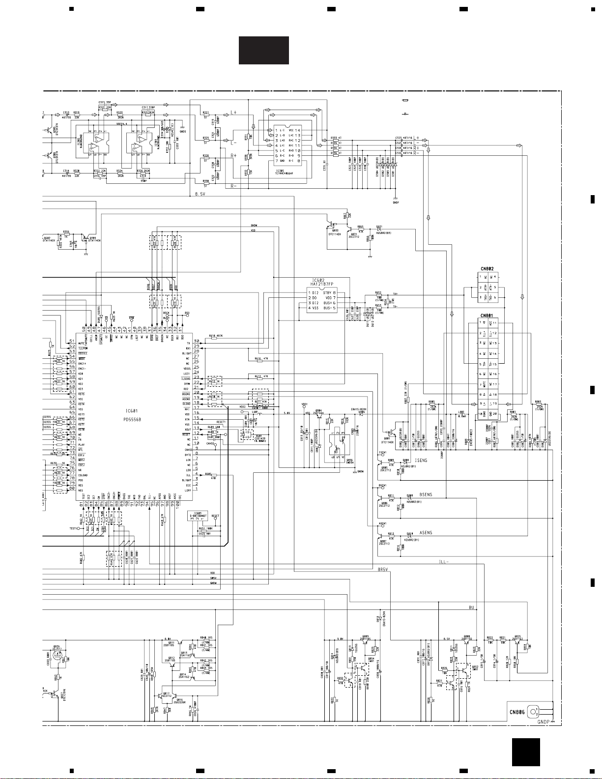
Unit Name : Main Unit
MISCELLANEOUS
IC 301 IC NJM2068MD
IC 302 IC NJM2068MD
IC 303 IC NJM2068MD
IC 305 IC TC74HC4066AF
IC 601 IC PD5556B
IC 602 IC HA12187FP
IC 603 IC S-80730ANDT
IC 701 IC PD5575B
Q 301 Transistor DTC343TK
Q 302 Transistor DTC343TK
Q 303 Transistor DTC343TK
Q 304 Transistor DTC343TK
Q 305 Transistor DTC343TK
Q 306 Transistor DTC343TK
Q 307 Transistor DTC343TK
Q 308 Transistor DTC343TK
Q 309 Transistor DTA114EK
Q 601 Transistor 2SA1162
Q 602 Transistor DTA114EK
Q 603 Transistor DTA114EK
Q 701 Transistor DTA144EK
Q 702 Transistor DTA114EK
Q 801 Transistor DTC114EK
Q 804 Transistor 2SD1664
Q 805 Chip Transistor 2SC2712
Q 806 Chip Transistor 2SC2712
Q 807 Chip Transistor 2SC2712
Q 808 Transistor 2SB1132
Q 809 Transistor 2SB1185
Q 811 Transistor 2SB1185
Q 812 Transistor 2SB1185
Q 813 Transistor 2SA1162
Q 814 Transistor 2SA1162
Q 816 Transistor 2SD2226K
Q 817 Chip Transistor 2SC2712
Q 822 Transistor 2SB1132
Q 823 Transistor DTC123YK
Q 824 Transistor DTA114EK
Q 825 Transistor 2SA1162
Q 826 FET 2SJ517
Q 827 Transistor DTC123YK
Q 828 Transistor DTA114EK
Q 829 FET 2SJ517
Q 830 Transistor DTC123YK
Q 831 Chip Transistor 2SC2712
Q 833 Transistor DTC114EK
Q 852 Transistor IMX1
Q 854 Transistor IMX1
Q 856 Transistor IMD3A
D 301 Diode UDZ20(B)
D 302 Diode UDZ20(B)
D 303 Diode UDZ20(B)
D 304 Diode UDZ20(B)
D 305 Diode HZU4LL(C)
D 601 Diode 1SS355
D 605 Diode 1SS355
D 608 Diode 1SS355
D 609 Diode 1SS355
D 610 Diode 1SS355
D 611 Diode UDZ18(B)
D 612 Diode UDZ18(B)
D 701 Diode 1SS355
D 801 Diode 1SS355
D 802 Diode UDZS5R6(B)
D 803 Diode ERC05-10BE3
D 804 Diode 1SS355
D 805 Diode UDZ20(B)
D 806 Diode ERA15-02VH
D 807 Diode UDZS5R6(B)
D 808 Diode HZU8R2(B1)
D 809 Diode HZU8R2(B1)
D 810 Diode HZU8R2(B1)
D 811 Diode 1SS355
D 812 Diode HZU8R2(B1)
D 813 Diode 1SS355
D 814 Diode HZU8R2(B3)
D 819 Diode ERA15-02VH
D 821 Diode HZU8R2(B3)
L 601 Inductor LCTB4R7K3216
L 701 Inductor LCTB4R7K3216
L 801 Choke Coil 0.8mH CTH1239
TH 701 Thermistor CCX1037
X 601 Radiator 10.00MHz CSS1428
X 701 Radiator 6.290MHz CSS1451
RESISTORS
R 301 RS1/10S122J
R 302 RS1/10S122J
R 303 RS1/10S473J
R 304 RS1/10S473J
R 307 RS1/10S123J
R 308 RS1/10S123J
R 309 RS1/10S183J
R 310 RS1/10S183J
R 311 RS1/10S223J
R 312 RS1/10S223J
R 313 RS1/10S911J
R 314 RS1/10S911J
R 315 RS1/10S473J
R 316 RS1/10S473J
R 317 RS1/10S911J
R 318 RS1/10S911J
R 319 RS1/10S223J
R 320 RS1/10S223J
R 321 RS1/10S223J
R 322 RS1/10S223J
=====Circuit Symbol and No.===Part Name Part No.
--- ------ ------------------------------------------ -------------------------
54
A
Page 55

55
FX-MG8006ZT,MG8006ZT-91,MG8506ZT,MG8506ZT-91
R 323 RS1/10S222J
R 324 RS1/10S222J
R 325 RS1/10S222J
R 326 RS1/10S222J
R 327 RS1/10S510J
R 328 RS1/10S510J
R 329 RS1/10S510J
R 330 RS1/10S510J
R 331 RS1/10S103J
R 332 RS1/10S153J
R 333 RS1/10S470J
R 334 RS1/10S470J
R 335 RS1/10S470J
R 336 RS1/10S470J
R 337 RS1/10S103J
R 338 RS1/10S392J
R 341 RS1/10S302J
R 342 RS1/10S302J
R 343 RS1/10S104J
R 344 RS1/10S104J
R 345 RS1/10S223J
R 355 RS1/10S472J
R 356 RS1/10S102J
R 602 RS1/10S473J
R 605 RS1/10S471J
R 608 RS1/10S102J
R 609 RS1/10S681J
R 610 RA3C102J
R 611 RA3C473J
R 612 RA2CQ102J
R 613 RS1/10S473J
R 616 RS1/10S473J
R 618 RS1/10S472J
R 619 RA2CQ102J
R 620 RA2CQ473J
R 621 RA3C102J
R 622 RA3C473J
R 623 RS1/10S102J
R 624 RS1/10S103J
R 625 RA3C102J
R 626 RA3C473J
R 627 1kΩ CCN1120
R 628 47kΩ CCN1131
R 629 RS1/10S102J
R 631 RA3C102J
R 632 1kΩ CCN1120
R 633 RS1/10S473J
R 634 RS1/10S473J
R 635 RS1/10S102J
R 637 RA2CQ473J
R 638 RS1/10S102J
R 639 RA2CQ102J
R 640 RA3C102J
R 641 47kΩ CCN1131
R 642 RS1/10S102J
R 643 RA3C102J
R 644 RS1/10S681J
R 645 RA3C102J
R 646 RA3C473J
R 649 RS1/10S473J
R 651 RS1/10S104J
R 652 RS1/4S101J
R 653 RS1/4S101J
R 654 RS1PMF680J
R 701 RS1/10S433J
R 702 RS1/10S103J
R 703 RS1/10S222J
R 704 RS1/10S103J
R 705 RS1/10S102J
R 706 RA2CQ222J
R 707 RA2CQ103J
R 708 330Ω CCN1116
R 709 RA2CQ222J
R 710 RS1/10S104J
R 711 RS1/10S331J
R 712 RS1/10S103J
R 713 RA2CQ102J
R 714 RA2CQ222J
R 715 RA2CQ103J
R 716 RA2CQ102J
R 717 RS1/10S102J
R 718 RS1/10S471J
R 719 RS1/10S102J
R 720 RA2CQ471J
R 722 RA2CQ222J
R 723 RA2CQ473J
R 724 RS1/10S102J
R 725 RA3C471J
R 726 RA2CQ102J
R 727 RA2CQ102J
R 728 470Ω CCN1117
R 729 470Ω CCN1117
R 730 470Ω CCN1117
R 731 RS1/10S471J
R 732 RS1/10S912J
R 733 RS1/10S102J
R 734 2.2kΩ CCN1121
R 735 RS1/10S273J
R 736 RS1/10S512J
R 737 RS1/10S104J
R 738 RS1/10S154J
R 739 RS1/10S103J
R 801 RS1/8S222J
R 802 RS1/8S472J
R 803 RS1/8S222J
R 804 RS1/8S472J
R 805 RS1/8S222J
R 806 RS1/8S472J
R 807 RS1/8S221J
R 809 RS1/10S473J
R 810 RS1/10S104J
R 811 RS1/10S473J
R 812 RS1/10S104J
R 813 RS1/10S473J
R 814 RS1/10S104J
R 815 RS1/10S223J
R 816 RS1/10S122J
R 820 RS1/10S123J
R 821 RS1/10S103J
R 822 RS1/10S103J
R 823 RS1/10S223J
R 824 RS1/10S102J
R 825 RS1/10S331J
R 826 RS1/10S103J
R 827 RS1/10S471J
R 828 RS1/10S102J
R 829 RS1/10S223J
R 830 RS1/10S221J
R 831 RS1/10S331J
R 832 RS1/10S471J
=====Circuit Symbol and No.===Part Name Part No.
--- ------ ------------------------------------------ -------------------------
=====Circuit Symbol and No.===Part Name Part No.
--- ------ ------------------------------------------ -------------------------
Page 56

56
FX-MG8006ZT,MG8006ZT-91,MG8506ZT,MG8506ZT-91
R 833 RS1/10S102J
R 840 RS1/4S1R5J
R 841 RS1/4S1R5J
R 842 RS1/4S1R5J
R 843 RS1/4S1R5J
R 844 RS1/10S471J
R 845 RS1/10S471J
R 846 RS1/10S105J
R 847 RS1/10S361J
R 848 RS1/10S1501D
R 849 RS1/10S2701D
R 856 RS1/10S103J
R 857 RS1/10S102J
R 859 RS1/10S103J
R 860 RS1/10S103J
R 861 RS1/10S103J
R 862 RS1/10S102J
R 863 RS1/10S103J
R 864 RS1/10S102J
R 865 RS1/10S473J
R 866 RS1/10S104J
R 867 RS1/10S223J
CAPACITORS
C 301 4.7µF/35V CCH1016
C 302 4.7µF/35V CCH1016
C 305 4.7µF/35V CCH1016
C 306 4.7µF/35V CCH1016
C 307 4.7µF/35V CCH1016
C 308 4.7µF/35V CCH1016
C 309 CCSQCH330J50
C 310 CCSQCH330J50
C 311 4.7µF/35V CCH1016
C 312 4.7µF/35V CCH1016
C 313 4.7µF/35V CCH1016
C 314 4.7µF/35V CCH1016
C 315 CCSQCH330J50
C 316 CCSQCH330J50
C 317 CKSQYB331K50
C 318 CKSQYB331K50
C 319 CKSQYB682K50
C 320 CKSQYB682K50
C 321 CKSQYB682K50
C 322 CKSQYB682K50
C 323 CEALNP4R7M16
C 324 CEALNP4R7M16
C 325 CEALNP4R7M16
C 326 CEALNP4R7M16
C 327 CCSQCH101J50
C 328 CCSQCH101J50
C 329 CCSQCH101J50
C 330 CCSQCH101J50
C 331 CKSQYB104K50
C 333 CKSQYB103K50
C 334 CEJA101M6R3
C 335 CEJA101M16
C 336 CKSQYB104K50
C 337 4.7µF/35V CCH1016
C 338 4.7µF/35V CCH1016
C 341 CKSQYB104K50
C 342 CEAL4R7M16
C 343 CEAL100M16
C 601 CKSQYB102K50
C 603 CEAL100M16
C 604 CKSQYB103K50
C 605 CKSQYB103K50
C 606 CCSQCH101J50
C 607 CCSQCH101J50
C 608 CCSQCH101J50
C 609 CCSQCH101J50
C 610 CCSQCH101J50
C 611 CCSQCH101J50
C 612 CCSQCH101J50
C 615 CCSQCH101J50
C 616 CCSQCH101J50
C 617 CCSQCH101J50
C 618 CCSQCH102J50
C 619 CCSQCH102J50
C 620 CCSQCH102J50
C 621 CCSQCH102J50
C 622 CCSQCH102J50
C 625 CKSQYB103K50
C 626 CKSQYB103K50
C 627 CKSQYB221K50
C 628 CKSQYB221K50
C 630 CKSQYB102K50
C 701 CKSQYB102K50
C 702 CKSQYB102K50
C 704 CKSQYB102K50
C 705 CKSQYB102K50
C 706 CKSQYB102K50
C 711 CKSQYB102K50
C 712 CKSQYB102K50
C 717 CKSQYB102K50
C 721 CKSQYB104K50
C 722 CEAL100M16
C 723 CKSQYB103K50
C 724 CKSQYB102K50
C 725 CKSQYB102K50
C 726 CKSQYB102K50
C 727 CKSQYB102K50
C 728 CCSQCH101J50
C 801 CKSQYB102K50
C 802 CEAL1R0M50
C 803 CKSQYB102K50
C 804 2200µF/16V CCH1186
C 805 CKSQYB473K50
C 806 CKSQYB102K50
C 807 CEAL1R0M50
C 808 CKSQYB102K50
C 809 2200µF/16V CCH1186
C 811 CCSQCH101J50
C 812 CKSQYB103K50
C 813 CEJA330M10
C 814 CEAL1R0M50
C 815 CEAL1R0M50
C 816 CKSQYB103K50
C 817 CEJA101M16
C 818 CKSQYB103K50
C 819 100µF/10V CCH1282
C 820 CKSQYB103K50
C 824 CKSQYB472K50
C 825 100µF/10V CCH1282
C 829 CKSQYB103K50
C 831 CKSQYB103K50
C 833 CKSQYB102K50
C 834 CKSQYB102K50
C 835 CKSQYB102K50
C 838 CEAT102M16
=====Circuit Symbol and No.===Part Name Part No.
--- ------ ------------------------------------------ -------------------------
=====Circuit Symbol and No.===Part Name Part No.
--- ------ ------------------------------------------ -------------------------
Page 57

57
FX-MG8006ZT,MG8006ZT-91,MG8506ZT,MG8506ZT-91
C 893 CKSQYB222K50
C 894 CKSQYB222K50
C 896 CKSQYB222K50
C 897 CKSQYB222K50
Unit Number : CWM6872
Unit Name : SW Unit
MISCELLANEOUS
D 921 LED SML210FT
D 922 LED SML210FT
D 923 LED SML210FT
D 924 LED SML210FT
D 925 LED SML210FT
S 924 Switch(DCLOSE) CSN1052
IL 923 Lamp 8V 60mA CEL1649
IL 924 Lamp 8V 60mA CEL1649
RESISTORS
R 931 RS1/8S331J
R 932 RS1/8S331J
R 933 RS1/8S331J
R 934 RS1/8S331J
R 935 RS1/8S331J
CAPACITORS
C 921 CKSQYB104K25
C 922 CKSQYB104K25
C 923 CKSQYB102K50
C 924 CKSQYB102K50
C 925 CKSQYB102K50
C 926 CKSQYB104K25
C 927 CKSQYB104K25
C 928 CKSQYB104K25
Unit Number : CWM6860
Unit Name : Keyboard Unit
MISCELLANEOUS
IL 901 Lamp 8V 60mA CEL1531
IL 902 Lamp 8V 60mA CEL1531
IL 903 Lamp 8V 60mA CEL1531
IL 904 Lamp 8V 60mA CEL1531
IL 905 Lamp 8V 60mA CEL1531
IL 906 Lamp 8V 60mA CEL1531
IL 907 Lamp 8V 60mA CEL1531
VR 901 Switch CSD1058
VR 902 Encoder CSD1053
RESISTORS
R 992 0Ω CCN1110
R 994 RS1/10S0R0J
R 996 RS1/10S0R0J
Unit Number : CWX2421
Unit Name : CD Core Unit(Servo Unit)
MISCELLANEOUS
IC 101 IC UPC2572GS
IC 201 IC UPD63702AGF
IC 301 IC BA5986FM
Q 101 Transistor 2SD1664
Q 102 Transistor UMD2N
D 301 Diode 1SR154-400
L 201 Inductor LCYBR15J1608
L 202 Inductor LCYBR15J1608
X 201 Ceramic Resonator 16.934MHz CSS1457
EF 201 Filter CCG1076
EF 202 Filter CCG1076
RESISTORS
R 101 RS1/8S100J
R 102 RS1/8S120J
R 104 RS1/16S822J
R 105 RS1/16S682J
R 106 RS1/16S183J
R 107 RS1/16S822J
R 108 RS1/16S333J
R 109 RS1/16S683J
R 110 RS1/16S134J
R 111 RS1/16S273J
R 112 RS1/16S222J
R 113 RS1/16S103J
R 114 RS1/16S103J
R 115 RS1/16S102J
R 116 RS1/16S163J
R 117 RS1/16S163J
R 120 RS1/16S101J
R 121 RS1/16S101J
R 201 RS1/16S104J
R 202 RS1/16S103J
R 203 RS1/16S332J
R 204 RS1/16S752J
R 205 RS1/16S752J
R 206 RS1/16S101J
R 250 RS1/16S331J
R 251 RS1/16S331J
R 252 RS1/16S331J
R 253 RS1/16S331J
R 254 RS1/16S331J
R 255 RS1/16S471J
R 256 RS1/16S471J
R 263 RS1/16S471J
R 270 RS1/16S101J
R 271 RS1/16S101J
R 274 RS1/16S471J
R 277 RS1/16S471J
R 301 RS1/16S103J
R 302 RS1/16S153J
R 303 RS1/16S103J
R 304 RS1/16S273J
R 305 RS1/16S103J
R 306 RS1/16S752J
R 307 RS1/16S103J
R 308 RS1/16S103J
R 309 RS1/16S471J
R 311 RS1/16S471J
CAPACITORS
C 101 CEV101M6R3
C 102 CKSQYB104K16
C 103 CEV470M6R3
C 104 CKSQYB334K16
C 105 CCSRCH240J50
C 106 CKSRYB222K50
C 107 CEV4R7M35
C 108 CKSRYB273K25
C 109 CCSRCH101J50
C 110 CKSQYB104K16
C 111 CKSRYB332K50
C 112 CKSQYB473K16
C 113 CKSRYB103K25
C 114 CKSRYB391K50
C 115 CCSRCH121J50
=====Circuit Symbol and No.===Part Name Part No.
--- ------ ------------------------------------------ -------------------------
=====Circuit Symbol and No.===Part Name Part No.
--- ------ ------------------------------------------ -------------------------
B
C
E
Page 58

58
FX-MG8006ZT,MG8006ZT-91,MG8506ZT,MG8506ZT-91
C 116 CKSRYB682K50
C 117 CKSRYB333K16
C 118 CKSQYB334K16
C 119 CKSQYB334K16
C 120 CKSQYB334K16
C 121 CKSQYB334K16
C 122 CKSQYB104K16
C 123 CKSRYB472K50
C 124 CKSQYB104K16
C 125 CCSRCH5R0C50
C 126 CKSRYB153K25
C 127 CKSRYB102K50
C 201 CKSQYB334K16
C 202 CKSQYB104K16
C 203 CKSQYB104K16
C 204 CKSRYB471K50
C 207 CKSQYB683K16
C 208 CKSRYB821K50
C 209 CKSRYB273K25
C 210 CKSQYB334K16
C 211 CKSQYB334K16
C 212 CKSQYB334K16
C 213 10µF/10V CCH1349
C 301 CEV101M10
C 302 CEV101M10
Unit Number : CWX2422
Unit Name : CD Core Unit(STS Unit)
MISCELLANEOUS
IC 501 IC CXD2511R
IC 502 IC
MSM514400DP-60TS
IC 601 IC AK4321VF
IC 701 IC BA05SFP
IC 801 IC LB1836M
IC 802 IC LB1836M
Q 801 Transistor DTA123JK
Q 802 Transistor UN2211
D 701 Diode 1SR154-400
D 702 Diode 1SR154-400
D 703 Diode 1SS355
D 704 Diode 1SS355
D 705 Diode 1SS355
D 706 Diode 1SS355
D 707 Diode 1SS355
D 708 Diode 1SS355
S 801 Spring Switch(LOAD) CSN1052
S 802 Spring Switch(DOOR) CSN1052
S 803 Spring Switch(MODE) CSN1052
EF 701 Filter CCG1051
EF 702 Filter CCG1051
EF 703 Filter CCG1051
RESISTORS
R 501 RS1/16S102J
R 502 RS1/16S202J
R 503 RS1/16S392J
R 504 RS1/16S822J
R 505 RS1/16S163J
R 506 RS1/16S512J
R 507 RS1/16S182J
R 508 RS1/16S222J
R 509 RS1/16S102J
R 510 RS1/16S102J
R 511 RS1/16S102J
R 512 RS1/16S102J
R 513 RS1/16S102J
R 514 RS1/16S471J
R 601 RS1/16S101J
R 602 RS1/16S101J
R 603 RS1/16S471J
R 604 RS1/16S471J
R 702 RS1/10S100J
R 716 RS1/16S471J
R 717 RS1/16S471J
R 718 RS1/16S471J
R 801 RS1/10S102J
CAPACITORS
C 501 CKSQYB334K16
C 502 CKSQYB334K16
C 503 CKSQYB334K16
C 504 CCSRCH471J50
C 506 CCSRCH221J50
C 601 CKSQYB334K16
C 602 CCSRCH221J50
C 603 CKSQYB334K16
C 604 CKSQYB334K16
C 605 CSZSR100M10
C 606 CKSQYB334K16
C 701 10µF/10V CCH1349
C 702 CEVL101M6R3
C 703 CKSQYB334K16
C 704 CKSQYB334K16
C 705 CCSRCH151J50
C 706 CCSRCH151J50
C 707 CCSRCH151J50
C 801 CKSQYB104K25
C 802 CKSQYB104K25
C 803 CEVL220M16
Unit Number :
Unit Name : PCB Unit(A)
D 891 Chip LED CL202IRXTU
D 892 Chip LED CL202IRXTU
Unit Number :
Unit Name : PCB Unit(B)
S 886 Spring Switch(ELV Home) CSN1052
S 887 Spring Switch(Clamp) CSN1051
Unit Number :
Unit Name : PCB Unit(C)
Q 881 Photo-transistor CPT230SCTD
D 883 Chip LED CL202IRXTU
S 885 Spring Switch(MAX DETECT) CSN1052
Unit Number :
Unit Name : PCB Unit(D)
Q 851 Photo-transistor CPT230SCTD
Q 852 Photo-transistor CPT230SCTD
Unit Number :
Unit Name : PCB Unit(E)
R 856 RS1/8S911J
R 857 RS1/8S821J
Unit Number :
Unit Name : Motor PCB(A)
Q 1 Photo-interrupter RPI-221
M 1 Motor Unit(Cam Gear) CXB6929
M 3 Motor Unit(ELV) CXB3175
=====Circuit Symbol and No.===Part Name Part No.
--- ------ ------------------------------------------ -------------------------
=====Circuit Symbol and No.===Part Name Part No.
--- ------ ------------------------------------------ -------------------------
G
M
H
I
J
L
F
Page 59

59
FX-MG8006ZT,MG8006ZT-91,MG8506ZT,MG8506ZT-91
Unit Number :
Unit Name : Motor PCB(B)
M 4 Motor Unit(Carriage) CXB3178
M 5 Motor(Spindle) CXM1120
Unit Number :
Unit Name : Load Motor PCB
M 2 Motor Unit(Load) CXB3177
Unit Number :EWM1027
Unit Name :Deck Unit
MISCELLANEOUS
IC 251 IC HA12216F
IC 351 IC PA2020A
Q 271 Transistor 2SC4116
Q 351 Transistor 2SB1260
Q 352 Transistor 2SC4102
D 351 Diode 1SS355
VR 301 Semi-fixed 33kΩ(B) CCP1280
VR 302 Semi-fixed 33kΩ(B) CCP1280
RESISTORS
R 255 RS1/16S181J
R 256 RS1/16S181J
R 257 RS1/16S183J
R 258 RS1/16S183J
R 259 RS1/16S133J
R 260 RS1/16S133J
R 261 RS1/16S274J
R 262 RS1/16S274J
R 271 RS1/16S183J
R 272 RS1/8S0R0J
R 273 RS1/8S0R0J
R 274 RS1/8S0R0J
R 275 RS1/16S473J
R 276 RS1/16S104J
R 277 RS1/16S224J
R 278 RS1/16S104J
R 281 RS1/8S0R0J
R 282 RS1/8S0R0J
R 283 RS1/8S0R0J
R 284 RS1/8S0R0J
R 285 RS1/16S0R0J
R 288 RS1/16S0R0J
R 289 RS1/16S0R0J
R 291 RS1/8S0R0J
R 292 RS1/10S0R0J
R 293 RS1/10S0R0J
R 294 RS1/10S0R0J
R 321 RS1/8S0R0J
R 351 RS1/16S102J
R 352 RS1/16S102J
R 353 RS1/16S102J
R 354 RS1/16S102J
R 355 RS1/10S274J
R 356 RS1/10S202J
R 357 RS1/10S472J
R 358 RS1/10S103J
R 359 RS1/10S103J
R 360 RS1/10S102J
R 361 RS1/10S622J
R 362 RS1/8S181J
R 373 RS1/8S0R0J
R 374 RS1/8S0R0J
R 375 RS1/8S0R0J
R 401 RS1/16S123J
R 402 RS1/16S332J
R 403 RS1/16S911J
R 404 RS1/16S274J
CAPACITORS
C 251 CKSRYB391K50
C 252 CKSRYB391K50
C 253 CKSRYB391K50
C 254 CKSRYB391K50
C 255 CKSRYB103K50
C 256 CKSRYB103K50
C 271 CEJA1R0M50
C 272 CKSQYB104K16
C 301 CKSQYB104K16
C 302 CKSQYB104K16
C 309 CKSQYB104K16
C 310 CKSQYB104K16
C 351 CKSYB224K25
C 352 CKSQYB392K50
C 353 CKSQYB103K50
C 354 CKSQYB103K50
C 355 CKSYB104K50
C 356 CKSQYB103K50
C 401 CKSRYB472K50
C 402 CKSYB334K25
C 403 CKSRYB223K25
C 404 CKSRYB103K50
C 405 CKSRYB333K16
Unit Number :
Unit Name : PCB Unit
L 1 Inductor ETH0002
S 1 Switch (LOAD) ESG1004
S 2 Switch (70µs) ESG1004
EGN 1 Photo-Interrupter EGN1005
Unit Number :
Unit Name : Reel PCB
EGN 2 Photo-Interrupter EGN1006
EGN 3 Photo-Interrupter EGN1006
Miscellaneous Parts List
Pickup Unit(Service)(P8) CXX1313
C 1 CEAL4R7M35
M 1 Motor Unit (Main) EXA1499
M 2 Motor Unit (Sub) EXA1382
HD 1 Head Assy EXA1594
=====Circuit Symbol and No.===Part Name Part No.
--- ------ ------------------------------------------ -------------------------
=====Circuit Symbol and No.===Part Name Part No.
--- ------ ------------------------------------------ -------------------------
N
O
P
K
D
Page 60

FX-MG8006ZT,MG8006ZT-91,MG8506ZT,MG8506ZT-91
6. ADJUSTMENT
6.1 CASSETTE SECTION
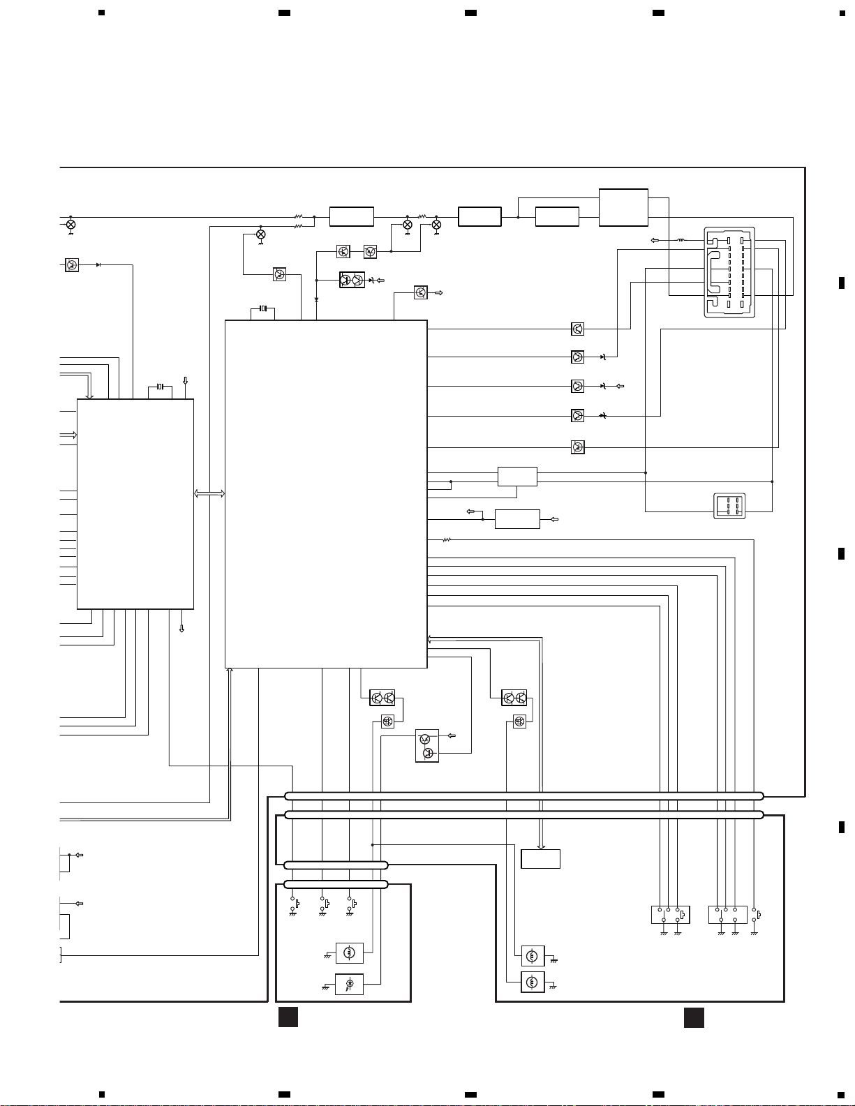
- Connection Diagram
H/U
FX-MG8006ZT/UC
Hide Away TUNER
GEX-T9006ZT/UC
DSP AMP
GM-9006ZT/E
Rear Controller
CD-R1976ZT/E
Electro Multi Vision
Navi ECU
25P
10P18P
14P 10P8P 6P
16P
12P 10P18P
25P
20P 10P
8P
6P 14P 8P
BULLET
CONNECTOR
BULLET
CONNECTOR
BULLET
CONNECTOR
6P20P
12P16P 25P
BULLET
CONNECTOR
12P25P
8P
GGD1169
GGD1232
GGD1234
GGD1239
VR302
mV
Meter(1)
VR301
L-CH
R-CH
Pin2
Pin3
CN251
DECK UNIT
GGD1121
FX-MG8506ZT/UC
Main Unit
CN301
60
DOLBY NR ADJUSTMENT
No. Test Tape Adjustment Point Adjustment Method
(Switch Position)
1 NCT-150 VR301(Lch),VR302(Rch) mV Meter(1) : –8.24dBm(300mV)±1dB
(400Hz,200nwb/m) (DOLBY NR Switch : OFF)
Page 61

61
FX-MG8006ZT,MG8006ZT-91,MG8506ZT,MG8506ZT-91
• Note :
The grating angle of the PU unit cannot be adjusted after the PU unit is changed. The PU unit in the CD
mechanism module is adjusted on the production line to match the CD mechanism module and is thus the best
adjusted PU unit for the CD mechanism module. Changing the PU unit is thus best considered as a last resort.
However, if the PU unit must be changed, the grating should be checked using the procedure below.
• Purpose :
To check that the grating is within an acceptable range when the PU unit is changed.
• Symptoms of Mal-adjustment :
If the grating is off by a large amount symptoms such as being unable to close tracking, being unable to perform
track search operations, or taking a long time for track searching.
• Method :
• Measuring Equipment • Oscilloscope, Two L.P.F.
• Measuring Points • E, F, REFOUT
• Disc • ABEX TCD-784
• Mode • TEST MODE
• Checking Procedure
1. In test mode, load the disc and switch the 5V regulator on.
2. Using the SEEK UP and SEEK DOWN buttons, move the PU unit to the innermost track.
3. Press key 5 to close focus, the display should read "91". Press key 3 to implement the tracking balance
adjustment the display should now read "81". Press key 5 4 times. The display will change, returning to "81" on
the fourth press.
4. As shown in the diagram above, monitor the LPF outputs using the oscilloscope and check that the phase
difference is within 75° . Refer to the photographs supplied to determine the phase angle.
5. If the phase difference is determined to be greater than 75° try changing the PU unit to see if there is any
improvement. If, after trying this a number of times, the grating angle does not become less than 75° then the
mechanism should be judged to be at fault.
• Note
Because of eccentricity in the disc and a slight misalignment of the clamping center the grating waveform may be
seen to "wobble" ( the phase difference changes as the disc rotates). The angle specified above indicates the
average angle.
• Hint
Reloading the disc changes the clamp position and may decrease the "wobble".
100kΩ
390pF
100kΩ
390pF
E
REFOUT
F
Xch Ych
Oscilloscope
L.P.F.
L.P.F.
E
F
REFOUT
REFOUT
CD CORE UNIT(SERVO UNIT)
6.2 CHECKING THE GRATING AFTER CHANGING THE PICKUP UNIT
Page 62

62
FX-MG8006ZT,MG8006ZT-91,MG8506ZT,MG8506ZT-91
Grating waveform
Ech → Xch 20mV/div, AC
Fch → Ych 20mV/div, AC
45°
0°
75°
60°
30°
90°
Page 63

63
FX-MG8006ZT,MG8006ZT-91,MG8506ZT,MG8506ZT-91
7. GENERAL INFORMATION
7.1 DIAGNOSIS
7.1.1 TEST MODE
- CD Test Mode
1) Precautions on Adjustment
• The unit employs a single voltage (+5V) for the
regulator, thus the reference potential of the signal is
RFOUT (approximately 2.5V) rather than GND.
Inadvertent contact of REFOUT and GND during
adjustment can result not only in disabling normal
potential measurement but also in exposing the
pickup to strong impacts due to malfunctioning of the
servo. Therefore, you are requested to observe the
following precautions.
• Make sure that the negative probe of the measuring
instrument is not connected to RFOUT or GND.
Special care must be exercised so that the channel 1
negative probe may not be connected to the
oscilloscope and the channel 2 negative probe to
GND. Since the frame of the measuring instrument is
usually at the same potential as the negative probe,
the frame of the measuring instrument must be
changed to floating status.
When RFOUT is inadvertently connected to GND, you
must immediately turn off the regulator or power
supply.
• The regulator must be turned off before mounting or
dismounting filters or wiring materials.
• You should not start adjustment or measurement
immediately after the regulator is turned on. It is
recommended to run the player for approximately
one minute so that it may stabilize.
• When the test mode is turned on, various protective
functions from the software become unavailable.
Thus, you must make sure that undesirable electric or
mechanical shocks are not be given to the system.
• This model employs a photo-transistor for detecting
discs at their loading or ejection. Thus, if its outer
case is removed during repair work and internal parts
are exposed to light of strong intensity, malfunctions
including the following can result:
∗ The eject button becomes inoperable during play.
Pressing the eject button does not eject a disc and
play is continued.
∗ Loading becomes unavailable.
If a malfunction is recognized, appropriate remedial
actions must be taken. Such actions include
changing the light source position, changing the unit
position and applying a cover to the photo-transistor.
• When you press the EJECT key to eject a disc, you
must not touch any other key until the ejection is
complete.
• If you press the TRACK UP or TRACK DOWN for the
focus search in the test mode, you must turn the
power off immediately. (Otherwise, the lens will be
forced to stick to the top or bottom, potentially
resulting in the burning of the actuator.)
2) Description of the Test Mode
• Turning on the Test Mode
See page 64.
• Ending the Test Mode
Apply the reset (the reset will be applied three
minutes after the power is turned from off).
• Operation of TR JUMPs (except 100TR) continues
after your finger has left the key. CRG, MOVE and
100TR JUMP are forced to the tracking close mode as
soon as the key is released.
• Turning the power on or off resets the JUMP MODE
to the Single TR.
Page 64

64
FX-MG8006ZT,MG8006ZT-91,MG8506ZT,MG8506ZT-91
[MSG]
Power Off
[5]
Focus Close/S-curve/
F, F0 Measurement
[TYPE]
Focus Mode Select
[3]
Tracking Servo
Close
[MSG]
Power ON
(T.OFFSET adjustment required)
00 00
[5]
Power ON
(T.OFFSET adjustment not required)
[3]
Mechanism Test Mode
Initial State
[TYPE]
New Test Mode
[MSG]
Power Off
[3]
Tracking Close
(AGC, Applicable Servo)
[TYPE]
Tracking Close
(No AGC, Applicable Servo)
[5]
Auto Adjustment Display
/Rough Servo
[4]
Tracking Balance
Adjustment
[5]
AGC
[TYPE]
CRG/TR Jump Count
Select
[TRACK UP]
CRG+/TR Jump+
[TRACK DOWN]
CRG–/TR Jump–
[6]
SPINDLE
Uniform/
Double Switching
[MSG]
Power Off
[3]
AGC/F.BIAS
Display Switching
or
[TRACK UP]
CRG+
[TRACK DOWN]
CRG-
[TRACK UP]
CRG+
[TRACK DOWN]
CRG-
[4]
Trackig Open
[4]
Trackig Open
*1
*6
*5
*3
*2
*2
*4
*1) Switching must take place in the following sequence.
MIN
SEC
00
00
()
MIN
SEC
99
99
S.Curve Check
MIN
SEC
01
01
Focus EQ Measurement.Focus Close
MIN
SEC
02 02
*2)
→→ → → →
9X(8X):91(81)
4 TR
92(82)
10 TR
93(83)
32 TR
94(84)
100 TR
95(85)
CRG Move
96(86)
Switching must take place in the following sequence.
*4)
→→→
F.AGC Gain T.AGC Gain F. BIAS Setting
(AGC Gain = (Current value/Initial value) x 20)
→→→
→→
Single TR /4TR / 10TR / 32TR / 100TR
Single TR
*3) Switching must take place in the following sequence.
It applies to the CRG Move and 100TR Jump alone.
Min/Sec (or Track No.)
*5) Switching must take place in the following sequence.
F.Cancel Display
*6) Switching must take place in the following sequence.
T.Offset Display T.Bal Display
Rough Servo.
(F.Bias value, F.Cancel value, T.Offset value, T.Bal value
= (Upper 8 bits of the setting (7F[H] to 80[H] + 128)/4
= 63[D] to 32[D] to 00[D]).
[Key]
[MSG]
[TRACK UP]
[TRACK DOWN]
[3]
[4]
[5]
[6]
[TYPE]
[2]
Operation
Test Mode
New Test Mode
Power ON/OFF
CRG+/TR Jump+
(Toward outer perimeter)
Tracking Close/AGC gain,
F.Bias adjustment value display switching
Auto Tracking Balance adjustment/
Tracking Open
Focus Close, S.Curve, F.EQ measurement/
Rough Servo/AGC
Focus Open
Focus Mode select/Tracking Close/
CRG*TR Jump Switching
CRG-/TR Jump(Toward inner perimeter)
Error occurrence time/
Cause display switching
Track+/FF
Track-/REV
Mode
RAMDOM
Auto/Manual switching
DISC UP
DISC UP
[EJECT]
[LOAD]
DISC Eject
DISC Eject
DISC Load
DISC Load
Source CD
Test Mode In
[CD] or [DISC]
TRK MIN
SEC
[TRACK UP] + [AM]
[Key]
Contents
Display
Diag. Mode In
[1] + [6] + [DISC] 3 times
PBUS TEST
Diag. off
[DISC] 3sec
TRK MIN
SEC
00
99 99
TRK MIN
SEC
99
72 0*
TRK MIN
SEC
**
TRK MIN
SEC
91 91
TRK MIN
SEC
91
0X 0X
TRK MIN
SEC
0X
00 00
TRK MIN
SEC
00
99 99
TRK MIN
SEC
99
or
00 00
TRK MIN
SEC
00
99 99
TRK MIN
SEC
99
or
00 00
TRK MIN
SEC
00
99 99
TRK MIN
SEC
99
TRK MIN
SEC
*7
*7
XX XX
TRK MIN
SEC
XX
XX XX
TRK MIN
SEC
XX
?? ??
TRK MIN
SEC
??
or
8X 8X
TRK MIN
SEC
8X
9X 9X
TRK MIN
SEC
9X
or
8X 8X
TRK MIN
SEC
8X
9X 9X
TRK MIN
SEC
9X
8X 8X
TRK MIN
SEC
8X
TRK MIN
SEC
?? ??
TRK MIN
SEC
??
XX XX
TRK MIN
SEC
XX
XX XX
TRK MIN
SEC
XX
XX XX
TRK MIN
SEC
XX
XX
TRK MIN
SEC
XX
or
8X 8X
TRK MIN
SEC
8X
9X 9X
TRK MIN
SEC
9X
XX XX
TRK MIN
SEC
XX
or
8X 8X
TRK MIN
SEC
8X
9X 9X
TRK MIN
SEC
9X
[MSG]
Power Off
TRK MIN
SEC
[1]
DISC DOWN
DISC DOWN
B0H
B1H
B2H
B3H
B4H
B5H
B6H
B8H
A8H
A9H
D1-D6
61-66
*7)
Sound is unavailable even after the tracking has been closed
(this trouble results when the IC for the STS is not controlled
in the test mode).
•
•
•
Operation of TR JUMPs other than 100TR is continued after your finger has left the key.
CRG Move and 100TR Jump are forced to the Tracking Close Mode when the key is released.
Powering on or off resets the Jump Mode to the Single TR (91).
When ending the test mode, apply the reset (the reset is applied in three minutes from powering off).
Note:
•When you pressed the [TRACK UP] or [TRACK DOWN] key during the Focus Search, you must turn the power off immediately
(otherwise, the lens can stick resulting in actuator damages).
[MSG]
[TYPE]
[ASL]
[PTY]
[P.SCAN]
[ASL]
EW model
ES model
- CD Player Flow Chart
Page 65

65
FX-MG8006ZT,MG8006ZT-91,MG8506ZT,MG8506ZT-91
[MSG] [3]
CAMMOTOR
select
[4]
ELVMOTOR
select
[5]
LOADMOTOR
select
[3]
Mechanism Test In
Initial State
[MSG]
CD Test Mode
[TYPE]
New Test Mode
Source CD
Test Mode In
[6]
CAM+LOADMOTOR
select
[TRACK UP]
MOTOR FWD drive
[Key]
[MSG]
[TRACK UP]
[TRACK DOWN]
[3]
[4]
[5]
[6]
Operation
Mechanism Test is initialized.
Valid only when the motor selected (using the
[F3] to [F6] keys) is driven in FWD direction.
CAMMOTOR is selected.
[5]
CD Test Mode
[TRACK DOWN]
MOTOR REV drive
Valid only when the motor selected (using the
[F3] to [F6] keys) is driven in REV direction.
ELVMOTOR is selected.
LOADMOTOR is selected.
CAM + LOADMOTOR is selected.
<Screen Display during Mechanism Test Mode>
MIN : Upper (10th order):
Type of motors selected
Lower (order of 1): State of DISC
sensing phototransistor and switch
1* : CAM motor
2* : ELV motor
3* : LOAD motor
4* : CAM+LOAD motor
PH1 PH2
MAXSW
Display
L
H
L
H
L
H
L
H
L
L
H
H
L
L
H
H
L
L
L
L
H
H
H
H
*0
*1
*2
*3
*4
*5
*6
*7
L:H:Phototransistor is OPEN and switch is ON.
Phototransistor is CLOSE and switch is OFF.
SEC : 1 When ELV motor is selected, ELV position is displayed
01: ELV at home position (1st disc).
10: ELV at a position other than home (2nd to 6th).
11: ELV moving to a specified position. * Note 1.
00: Not used (for an error)
2 When CAM.LOAD motor is selected:
Indicates CAM SW (CAM gear) status.
SW1 (DOORSW)
SW2 (LOADSW)
SW3 (MODESW)
SW4 (CLAMPSW)
Display
10
30
31
21 20
222333 32
REV
FWD
Note 2
clamp
[CD] or [DISC]
TRK MIN
SEC
[TRACK UP] + [AM]
[1]
[EJECT]
DISC DOWN
DISC Eject
[LOAD]
DISC Load
❏ Operating Procedures:
1)
2)
3)
4)
Enter Diag and set on the CD test mode.
Subsequently, exit from Diag and set the source for the CD.
Turn on the Mechanism Test Mode using the [3] key.
Select the motor to be driven
using the [3] to [6] keys.
Press the [TRACK UP] or [TRACK DOWN] in this
state to drive the selected motor.
[Key]
Contents
Display
Diag. Mode In
[1] + [6] + [DISC] 3 times
PBUS TEST
Diag. off
[DISC] 3sec
72
0*
**
TRK MIN
SEC
00
00
00
TRK MIN
SEC
99
99
99
TRK MIN
SEC
72
1*
**
TRK MIN
SEC
72
2*
**
TRK MIN
SEC
72
3*
**
TRK MIN
SEC
72
4*
**
TRK MIN
SEC
72
**
**
TRK MIN
SEC
72
**
**
TRK MIN
SEC
CD Test mode
00
00
00
TRK MIN
SEC
TRK : 72
[2]
DISC UP
B0H
B1H
B2H
B3H
B4H
B5H
B6H
A8H
A9H
43H
60H
❏ Precautions
*
*
Note 1:
Note 2:
The keys are inoperable as long as operation of the mechanism is continued.
When driving the CAMMOTOR in 31 → 30 → 10 (in REV direction),
the elevation position must be at the EJECT/LOAD position (the top position).
When the elevation is situated at the Note 1 position, move of any motor
other than the REV is disabled.
Before performing the elevation, make sure that the CAM SW (switch) is
set to a position between 22 and 20.
As a rule, driving of the ELV MOTOR must be started immediately after
the CAMSW indication has changed from 22 to 20.
MIN
SEC
X*
TRK
72*
MIN
SEC
X*
TRK
72*
**
[MSG]
[TYPE]
[ASL]
[PTY]
[P.SCAN]
[ASL]
EW model
ES model
- CD Mechanism Test Mode Flow Chart
Page 66

66
FX-MG8006ZT,MG8006ZT-91,MG8506ZT,MG8506ZT-91
1
2
3
4
5
6
Select CAMMOTOR using [3], then press the [TRACK DOWN] while the disc is being clamped (CAMSW state is 32).
The CAMSW status indication sequentially changes through 32→33→23→22.
When the disc to be ejected is not identical with the disc being clamped, select the [4 ] ELVMOTOR in the vicinity of where
the display changes from 22 to 20, then match the elevation to the disc to be ejected according to the following procedures:
After selecting ELVMOTOR, lower the elevation until the ELV position display becomes 01 (1st disc) using the [TRACK DOWN].
Drive the elevation up until the display is changed to 10 using the [TRACK UP] . This is the elevation where the second disk is situated.
The next display of 10 tells you the elevation of the 3rd disc. Repeating this operation allows you to establish an elevation
matching each disc. (When the elevation is driven from the 1st through 6th disc, the status display changes as
01→11→10→11→10→11→10→11→10→11→10.)
(When the disc to be ejected coincides with the disc being clamped, the above operations are not necessary.)
Select the [3] CAMMOTOR and then, using the [TRACK DOWN], drive it until the display changes from 20 (or 22) to 21 and 31.
Select the [4] ELVMOTOR, then drive the tray of the disc to be ejected up to the EJECT/LOAD position (using the [TRACK UP]).
Select the [6] CAM+LOADMOTOR, then drive it in the REV direction until the display changes from 31 to 30 and 10.
The door will open immediately before the display changes to 10 and part of the disc will be pushed out.
When 10 is displayed, select the [5] LOADMOTOR, then drive it in REV direction until the disc is completely ejected.
❍ Operating Procedures for Ejecting a Clamped Disc
- Error No. Display
The error mode is turned on if a CD player becomes not playable or is forced to halt due to an error. Cause(s) of an
error will be indicated with numerical characters. The error-number-display function is intended to facilitate the
error analysis and resulting repair work.
(1) Error Code
Error code Category Troubles Description/Cause(s)
10 Electricity Carriage home error Unable to move to or from inner perimeter
→
Failure on home switch or carriage move trouble.
11 Electricity Focus search error Unable to set a focus
→
Scratches or stains on backside of the disc, severe vibrations,
CD-R is not written to the disc
(it can happen on the backside of the disc).
12 Electricity Spindle lock error Spindle lock unavailable, sub-code unreadable
Sub-code error
→
Failure on spindle, scratches on the disc, stains or strong
vibrations.
14 Electricity Mirror error MIRR signal error continues for 500 msec or more
→
Stains on the disc or strong vibrations.
17 Electricity Setup error AGC protection cannot be turned on in time or focus can be easily lost
→
Scratches or stains on the disc or strong vibrations.
19 Electricity Tracking Balance error Tracking error level is low or tracking balance adjustment is unavailable
→
Failure on the pickup or tracking-error circuit.
30 Electricity Search time-out Target address can't be reached
→
Failure on the carriage/tracking or scratches on the disc.
A0 System Error on power supply Ground fault of power supply (VD)
→
Failure on switching transistor or failure of power supply.
– High temperature Temperature error(High temperature).
stand-by
Error code AVC-LAN Error code
11, 12, 14, 17, 19, 30 ERROR1
10 ERROR3
A0 ERROR4
– WAIT
Page 67

67
FX-MG8006ZT,MG8006ZT-91,MG8506ZT,MG8506ZT-91
Code Name Description
20 Door OPENING While the mechanism is in operation, should have been closed a door
was opened.
21 Roller OFF time-out 4 seconds have elapsed before completing the roller OFF
(the cam gear has not been rotated to the roller-OFF end position).
22 Roller SET time-out 4 seconds have elapsed before completing the roller SET.
(Roller OFF time-out) (During the roller OFF operation, 4 seconds have elapsed while the cam
gear is rotating in REV direction.)
23 Door CLOSING Door can't be closed when the roller OFF has ended.
24 Cam started from invalid position The cam gear attempted to do roller OFF/roller SET from an invalid
position.
26 Foreign substance on photo-transistor Foreign substance was found on the photo-transistor when closing the
(before closing the door) door after the loading is complete.
An error will be indicated if the disc is still caught by the
photo-transistor after 4 seconds of forced eject.
29 Roller being caught Although the cam gear has been rotated up to the roller OFF end
position, the roller can't be moved to the standby position.
41 Lift DOWN time-out 4 seconds have elapsed before completing the lift DOWN operation.
42 Lift UP time-out 4 seconds have elapsed before completing the lift UP operation.
(Lift DOWN time-out) (During the lift DOWN operation, 4 seconds have passed with the cam
gear rotating in REV direction.)
45 Lift DOWN cam displacement The lift DOWN complete cam gear has been displaced from its
specified position.
52 EJECT time-out 8 seconds have elapsed before completing the EJECT operation.
An error will be indicated if the disc is still caught by the
photo-transistor after 4 seconds of forced eject.
57 Photo-transistor being caught When forced eject was employed for the Bup failure during loading or
after forced EJECT ejection,an error will be indicated if the disk is still caught by the
photo-transistor after 4 seconds of forced eject.
61 CRGIN time-out 10 seconds have elapsed before completing CRGIN operation.
(CRGOUT time-out) (During CRGOUT operation, 10 seconds have elapsed with the cam
gear rotating in REV direction.)
62 CRGOUT time-out 10 seconds have elapsed before completing the CRGOUT operation.
63 CRGOUT cam displacement Position of the CRGOUT complete cam gear has been displaced.
71 ELVUP time-out 2 seconds have elapsed before completing 1-stage UP.
72 ELVDN time-out 2 seconds have elapsed before completing 1-stage DOWN.
74 ELV displacement At the start of ELV, ELVSNS was not set to low.
(In case of starting from the 1st floor, ELHOME was not set to low.)
75 ELV counting error HLHOME was set to low though not on the 1st floor.
(There is a conflict between the floor number stored on the
microcomputer and the actual floor number.)
91 LOAD time-out 8 seconds have elapsed before completing the LOAD.
An error will be indicated if the disc is still caught by the
photo-transistor after 4 seconds of forced eject.
96 Settlement of foreign substance Unauthorized foreign substance such as 8 cm disc has been loaded.
An error will be indicated if the disc is still caught by the
photo-transistor after 4 seconds of forced eject.
* AVC-LAN Error code : ERROR3
Page 68

68
FX-MG8006ZT,MG8006ZT-91,MG8506ZT,MG8506ZT-91
7.1.2 DIAGNOSIS MODE
1. How to Enter Diagnostic Test Mode
Diagnostic Test Mode
Speed = 0 km/h, PKB = ON
Tail OFF to ON to OFF to ON to OFF in this sequence pressing the information switch.
Entering from the head unit
Press F1 and F6 (or F7 and F8) at the same time and press the Disc (or CD) button three times with (F1 pressed first).
2. How to exit from the diagnostic test mode
ACC OFF
3. Diagnosis MENU
When the diagnostic test mode is entered, the Diagnosis MENU screen is displayed.
Diagnosis MENU
Service Check
Display Check
Navigation Check
1 Service Check screen calling switch
2 Display Check screen calling switch
3 Navigation Check screen calling switch
Page 69

69
FX-MG8006ZT,MG8006ZT-91,MG8506ZT,MG8506ZT-91
4. Service test
Use the function key on the Diagnosis menu screen to select Service Check Mode.
Displaying test results
The results tested based on the information such as responses of each equipment to "System Test Execution" and
"Diagnostic Memory Presentation Request" and "Normal Diagnostic Notification" are displayed on the screen.
Display Meaning
OK No error code
Exchange An error code indicating that exchange is judged to be necessary is entered.
Check An error code indicating that diagnosis is judged to be necessary is entered.
Unconnected Although registration is performed at ACC ON, there is no response when "Service Test" is started.
Old Ver Some error code is entered in the object old diagnostic Ver. equipment.
No Response Disconnection is occurring after "Service Test" has been started.
1 Equipment names Names are displayed including succeeding fitted components.
2 Test results Test results are displayed in the notation of "OK", "Check" and "Exchange".
* "Exchange", "Check" and "Old Ver" are displayed as switches, and "Communication
Diagnosis" and "Individual Diagnosis" are called according to the operation.
3 Memory CLR Registered histories of the master equipment and all diagnostic memories of all equipment
switch are cleared. (Long pressing of three seconds)
4 Code CLR switch • Diagnostic memories of all equipment are cleared.
• System test results are cleared and the contents of screen display of the test results are
also cleared.
5 Recheck switch The test is re-executed.
6 MODE screen Processing returns to the MODE screen.
calling switch
1 Equipment names
6 MODE screen calling switch
5 Recheck switch
3 Memory CLR switch
4 Code CLR switch2 Test results
Service Check Mode MODE
Fr-DISPLAY
DSP AMP
MONET-ECU
MDCH
AUDIO H/U
TV-TUNER
CDCH
: OK
: OK
:
Code CLR
Memory CLR
Recheck
NAVI-ECU
Rr-CONT
1C1
G/W-ECU
RADIO
: OK
: NG
:
: Old
: CHEK
:
:
:
:
Page 70

70
FX-MG8006ZT,MG8006ZT-91,MG8506ZT,MG8506ZT-91
Calling the "Communication Diagnosis Detailed Information" or "Individual Diagnosis Detailed
Information" screen
• When test results are "Exchange", "Check" or "Old Ver", this display is used as a switch to switch to the detailed
display screen of "Communication Diagnosis" or "Individual Diagnosis" and to check the contents.
• If an "Individual Diagnosis" code is entered, the "Individual Diagnosis Detailed Information" screen is displayed.
• When an "Individual Diagnosis" code is not entered, the "Communication Diagnosis Detailed Information" screen is
displayed.
(Switching to both the detailed information screens is performed using the function key displayed on the screen.)
"Communication Diagnosis" detailed information screen
A "Communication Diagnosis" code is chosen and displayed in detail using the diagnostic code of the equipment
displayed as "Check" in the Service Check results.
2 Classification
1 Equipment name
3 Diagnostic code
9 Service Check switch
8 LAN Check switch
6 Frequency of occurrence
7 Code CLR switch
5 Connection confirmation number
4 Related equipment
address number
01-DB 160-72- 5
01-E5 -AF- 1
01-D6 -09- 2
01-DC 160-72- 1
01-E1 - 3
01-E6 170-41- 5
01-DC 160-72- 1
Unit Check Mode
Code Sub Code
: DSP AMP
Service
Code Sub Code
LAN Check
Code CLR
1 Equipment name Object equipment name
2 Classification Object logical address number
3 Diagnostic code Diagnostic code
4 Related equipment Physical address stored together with a diagnostic code (equipment code)
address number
5 Connection Connection confirmation number stored together with a diagnostic code
confirmation number
6
Frequency of occurrence
Frequency of occurrence of the same diagnostic code stored together with a diagnostic code
7 Code CLR switch The diagnostic information of object equipment is cleared.
(Long pressing of three seconds)
8 LAN Check switch The individual diagnosis detailed information screen is switched.
9 Service check switch The service test screen is switched.
Page 71

71
FX-MG8006ZT,MG8006ZT-91,MG8506ZT,MG8506ZT-91
"Individual Diagnosis" detailed information screen
Error codes of the equipment displayed as "Exchange" are displayed on the Service Check screen by being divided into
the current and previous errors.
Current error • Error codes which were entered in the system test are displayed. (Up to six items)
Previous error • Diagnostic memory collection results or contents of normal diagnostic notification are
displayed up to six
1 Equipment name Object equipment name
2 Classification Object logical address number
3 Diagnostic code Diagnostic code
4 Date and hour Year, month, hour, minute and second at the time when a diagnostic code occurred
(If time information is invalid, a blank is displayed.)
5 Code CLR switch The diagnostic information of object equipment is cleared.
(Long pressing of three seconds)
6 LAN Check switch The Communication Diagnosis detailed information screen is switched.
7
Service Check switch
The service test screen is switched.
1 Equipment name
7 Service Check switch
6 LAN Check switch
4 Date and hour
5 Code CLR switch
3 Diagnostic code2 Classification
58-61 98/04/20 12:00:00
58-63 98/07/01 10:41:05
01-21
58-61
58-63
Unit Check Mode
: NAVI- ECU
Service
LAN Check
Code CLR
Current Memory Occurred Data / Time
Page 72

72
FX-MG8006ZT,MG8006ZT-91,MG8506ZT,MG8506ZT-91
7.1.3 DISASSEMBLY
- Removing the Case (Fig.1)
Remove the two screws.
Remove the two screws and then remove the
Guide.
Remove the two screws.
Remove the two screws and then remove the
Case.
- Removing the Main Unit (Fig.3)
Remove the two screws.
Straighten the tabs at five locations indicated.
Remove the screw and then remove the Main
Unit.
Guide
Case
Cassette Mechanism Module
Grille Assy
Main Unit
Fig.1
Fig.2
Fig.3
- Removing the Grille Assy (Fig.2)
Remove the two screws and then remove the
Grille Assy.
- Removing the Cassette Mechanism Module
(Fig.2)
Remove the four screws and then remove the
Cassette Mechanism Module.
Page 73

73
FX-MG8006ZT,MG8006ZT-91,MG8506ZT,MG8506ZT-91
Fig.4
-
Removing the Chassis Unit (Fig.4)
Remove the seven screws and then remove
the Chassis Unit.
Chassis Unit
- Removing the Mechanism Assy (Fig.5)
1. Disconnect the Connector.
2. Remove the three screws A, and then remove the Holder and Damper.
3. Remove the two screws B, and then remove the Holder and Damper.
4. Remove the two springs C, the spring D and the spring E and then remove the Mechanism Assy.
Damper
Damper
Damper
Damper
Holder
Holder
Holder
Holder
Connector
Mechanism Assy
Fig.5
Page 74

74
FX-MG8006ZT,MG8006ZT-91,MG8506ZT,MG8506ZT-91
- How to remove the Tray Assy
1. Apply about 6V current to the Cam gear motor until
all holes match at the position (A) (elevation OK
position).
2. Hook the three springs B temporarily as shown in Fig.
5. While pushing the Tray holder lock arms (right and
left) in the direction (C), remove the Tray holder.
3. Lift up the Tray assy to remove it.
* Be careful not to remove the Tray hooks from the Tray
assy.
ELV motor
Cam gear motor
Approximately DC 6V
Tray holder
Tray holder lock arm
Tray holder
lock arm
Tray
hooks
Tray Assy
Fig.6
Fig. 7
Tray
hooks
Page 75

75
FX-MG8006ZT,MG8006ZT-91,MG8506ZT,MG8506ZT-91
10. Remove the screw, pressure spring and collar. Lift
up the Carriage mechanism assy to remove it.
* Screw tightening torque: 2.6kgfcm
Carriage
Mechanism Assy
Screw
Collar
Pressure spring
Fig. 9
- How to remove the Carriage Mech Assy
1. Insert a short pin into the flexible PCB of the Pickup
unit.
2. While opening the resin hooks, remove the cover
from the Servo unit.
3. Disconnect the flexible PCBs from the connectors
CN101 and CN301.
4. Remove the Tray holder and the Tray assy. (See
above)
5. Rotate the Cam gear motor until the positions of all
holes (E) match, then stop the motor.
(The Carriage Mech assy will stop as shown in the
Fig.8.)
* When the positions of all holes match, they will be
completely covered by the Carriage mech assy.
* To rotate the Cam Gear motor, see "How to remove
the Tray assy".
6. Unhook the spring A.
7. Remove the flexible holder B (while opening the
hooks).
8. Remove the flexible PCB (C) from the motor. (The
flexible PCB (C) has been stuck on the motor with
double-sided adhesive tape.)
9. Loosen the fixing screw and remove the flexible
holder.
Cover
CN101
CN301
Match the hole positions
Flexible
holder
Fig. 8
Short pin
Page 76

76
FX-MG8006ZT,MG8006ZT-91,MG8506ZT,MG8506ZT-91
- How to remove the Pickup unit
1. Remove the pulling spring, torsion spring and Eshaped ring. Then remove the Clamper arm.
* The spring (A) will be removed with the Clamper
arm.
2. Slide the Clamp UP lever (B) to remove it.
3. Loosen the 2 screws. Remove the feed-screw cover
by sliding it.
4. Remove the feed-screw pressure spring (D).
5. Loosen the 2 screws. Remove the feed-screw holder
(E).
6. Remove the belt.
7. Remove the Pickup unit together with the feed screw.
* Be careful not to lose the shaft holders at the both
ends of the feed screw.
* Be careful not to damage the 2 flexible PCBs(for the
Pickup and motor) when separating them. The
flexible PCBs have been stuck each other with
double-sided adhesive tape.
Clamper arm
E-shaped ring
Pulling spring
Torsion spring
White
Black
Pickup
unit
Feed screw
Belt
Carriage
motor
Fig. 10
Fig. 11
8. Loosen the 2 screws. Remove the plate spring and
the rack.
9. Pull out the feed screw from the Pickup unit.
Rack
Plate spring
Feed screw
Pickup
unit
Grease (White: KD-1)
Grease (Yellow:
PG-641)
Fig. 12
Grease (Yellow:
PG-641)
Page 77

77
FX-MG8006ZT,MG8006ZT-91,MG8506ZT,MG8506ZT-91
7.1.4 PCB LOCATIONS
D
A
C
B
J
L
O
K
M
E
I
N
MOTOR PCB(B)
CD CORE UNIT(STS UNIT)
G
PCB UNIT(C)
F
H
P
PCB UNIT(E)
PCB UNIT(A)
PCB UNIT(D)
LOAD MOTOR PCB
CD CORE UNIT(SERVO UNIT)
PCB UNIT(B)
MOTOR PCB(A)
MAIN UNIT
KEYBOARD UNIT
SW UNIT
DECK UNIT
REEL PCB
PCB UNIT
Page 78

78
FX-MG8006ZT,MG8006ZT-91,MG8506ZT,MG8506ZT-91
7.1.5 CONNECTOR FUNCTION DESCRIPTION
TXS+ ATX+
TXS- ATX-
SGND L+ R+
GND L- ILL- ACC
ILL+ +BMUTE TX+
R- TX-
Page 79

79
FX-MG8006ZT,MG8006ZT-91,MG8506ZT,MG8506ZT-91
- Pin Functions (PD5556B)
Pin No. Pin Name I/O Function and Operation
1 LOFF O LCD driver OFF output
2 ECE O Chip enable output for EEPROM
3 BLIGHT O Back Light ON/OFF output
4 ILL O LAMP power supply control
5 LDO O LCD driver data output
6 NC Not used
7 LCK O Clock output for LCD driver
8 BYTE VCC joint
9 CNVSS VSS joint
10,11 NC Not used
12 reset I Reset input
13 XOUT O Crystal oscillating element connection pin
14 VSS GND
15 XIN I Crystal oscillating element connection pin
16 VDD Power supply
17 nhi VDD joint
18 dload I CD load key input
19 asens I ACC power sense input
20 bsens I Back up power sense input
21 RX2 I IE-BUS data input
22 IPPW O IP-BUS driver power supply output
23 ilsens I Illumination sense input
24 LCE1 O Chip enable output pin for LCD driver
25 VDSEL GND
26,27 NC Not used
28 BLIGHT O Back Light ON/OFF output
29 RX1 I IE-BUS data input
30 TX O IE-BUS data output
31 BSO O P-BUS serial data output
32 BSI I P-BUS serial data input
33 BSCK O P-BUS clock output
34 NC Not used
35 BRXEN I/O P-BUS reception enable input/output
36 brst I P-BUS reset input
37 bsrq O P-BUS service request output
38,39 NC Not used
40 LRST O LCD driver reset output
41 EPM Not used
42–44 NC Not used
45 swvdd O Display microcomputer power supply output
46 CE Not used
47 sysmute O System mute output
48 ANSW O Analog SW output
49 CDILL O CD illumination output
50 TAPEMUTE O Tape mute output
51 MUTE O BUS mute output
52 illpow O Illumination power supply output
53 dssill O DSS illumination output
54 mode I AUDIO mode key input
55 ENC1+ I Encoder 1 (+) input
56 ENC1- I Encoder 1 (-) input
57 KD0 I Key return input
58 KD1 I Key return input
59 KD2 I Key return input
60 KD3 I Key return input
61 kst% O Key strobe output
62 VCC Power supply
7.2 IC
Page 80

80
FX-MG8006ZT,MG8006ZT-91,MG8506ZT,MG8506ZT-91
*PD5556B
IC's marked by* are MOS type.
Be careful in handling them because they are very
liable to be damaged by electrostatic induction.
Pin No. Pin Name I/O Function and Operation
63 kst$ O Key strobe output
64 VSS GND
65 KST3 O Key strobe output
66 kst@ O Key strobe output
67 kst! O Key strobe output
68 kst) O Key strobe output
69 MS I Music sense input
70 fR O Head forward/reverse select output
71 PLAY O MS gain select output
72 mtl I Cassette mechanism tape select input
73 cdej I CD eject key sense input
74 mdej I MD eject key sense input
75 csej I Tape eject key sense input
76 NR O Dolby NR ON/OFF select output
77 CSLOAD I Tape loading detect input
78 POS I Cassette mechanism position sense input
79 RES I Cassette mechanism reverse end sense input
80 NES I Cassette mechanism forward end sense input
81 TEST I Test mode input
82 SC2 O Cassette mechanism sub motor control output
83 SC1 O Cassette mechanism sub motor control output
84 CM O Cassette mechanism capstan motor control output
85 stby O Stand-by output
86 ENC2- I Encoder 2 (-) input
87 ENC2+ I Encoder 2 (+) input
88 power I POWER key input
89 BASS I A/D converter input from BASS volume (not used)
90 TRE I A/D converter input from TREBLE volume (not used)
91 MID I A/D converter input from MID volume (not used)
92 FAD I A/D converter input from FADER volume (not used)
93 BAL I A/D converter input from BALANCE volume (not used)
94 ILL- I Rheostat signal input
95 NC Not used
96 AVSS A/D GND
97 ANO GND
98 VREF I A/D converter reference voltage input
99 AVCC A/D VCC
100 EDI I Data input from EEPROM
30
31
50
51
80
81
100
1
Page 81

81
FX-MG8006ZT,MG8006ZT-91,MG8506ZT,MG8506ZT-91
- Pin Functions (PD5575B)
Pin No. Pin Name I/O Format Function and Operation
1 VDIN I Power supply short sensor input
2 doorsw I Door open position SW input
3 NC Not used
4 bsrq O C P-BUS service request output
5 clamp I DISC clamp SW input
6 elhome I ELV reset position SW input
7 XSCK O C CD LSI clock output
8 XSO O C CD LSI data output
9 XSI I CD LSI data input
10 xstb O C CD LSI strobe output
11 xrst O C CD LSI reset output
12 XA0 O C Control signal distinguishing data from microcomputer
13 VDCONT O C VD control output
14 NC Not used
15 bsens I Back up power sense input
16 BRXEN I/O C P-BUS reception enable input/output
17 loadsw I Loading position SW input
18 modesw I ELV OK position SW input
19 BSCK I/O C P-BUS serial clock input/output
20 BSO O C P–BUS serial data output
21 BSI I P–BUS serial data input
22 brst I P–BUS reset input
23 SBSY I Signal indicating head of subcode block
24 CNVSS I GND
25 reset I Reset input
26 POWER O C Servo/Mechanism power supply control output
27 CONT O C Servo driver output control
28 Xin I Crystal oscillating element connection pin
29 Xout O C Crystal oscillating element connection pin
30 VSS GND
31–38 NC Not used
39 TESTIN I Chip check program mode input
40 DCLOSE I Door close sense input
41 WDSL O C Data comparison area specification signal output
42 XWIH I Data write inhibit input
43 XEMP I Data read inhibit input
44 CHDT I Data comparison mode monitor input
45 CHM0 O C Data comparison mode output 0
46 CHM1 O C Data comparison mode output 1
47–49 NC Not used
50 XWRE O C DRAM WRT ENBL
51 XRDE O C DRAM READ ENBL
52 XQOK O C SUB-Q OK output
53 EMPH O C DAC emphasis output
54 SCONT O C Mode select output
55 LOAD O C PHOT power supply control
56 cdmute O C CD mute output
57 LO2 O C LOAD motor control terminal output 2
58 LO1 O C LOAD motor control terminal output 1
59 ELV2 O C ELV motor control terminal output 2
60 ELV1 O C ELV motor control terminal output 1
61 CG2 O C CAM motor control terminal output 2
62 CG1 O C CAM motor control terminal output 1
63 MIRR I CD LSI mirror detector input
64 LOCK I CD LSI spindle lock detector input
65 FOK I CD LSI FOK signal input
66–68 NC Not used
69 adena O C A/D reference voltage output
Page 82

82
FX-MG8006ZT,MG8006ZT-91,MG8506ZT,MG8506ZT-91
*PD5575B
1
20
21
40
41
60
61
100
Format Meaning
C C MOS
Pin No. Pin Name I/O Format Function and Operation
70 NC Not used
71 VCC VDD
72 VREF I A/D converter reference voltage input
73 AVSS A/D GND
74 ADRMON I The remainder amount address monitor input
75 EREF DRAM A/D reference voltage output
76 PH1 I Disc photo sense input 1
77 PH2 I Disc photo sense input 2
78 PH3 I Disc photo sense input 3
79 ELVSNS I ELV position photo sense input
80 TEMP I Temperature detector input
Page 83

83
FX-MG8006ZT,MG8006ZT-91,MG8506ZT,MG8506ZT-91
HA12216F
31
32
33
34
35
36
37
38
39
40
12 34567
8910
11
12
13
14
15
16
17
18
19
20
212223
24
25
26
27
28
29
30
MSGV(R)
MAOUT
MSI
MSDET
VCC
MSOUT
MSGV
F/R
120/70
NR
MOUT(L)
EQOUT(L)
TAI(L)
NC
RAI(L)
PBOUT(L)
NC
DET(L)
NC
MSGV(S)
NFI(L)
RIN(L)
RIP
FIN(L)
GND
GND
FIN(R)
VREF
RIN(R)
NFI(R)
M-OUT(R)
EQOUT(R)
TAI(R)
BIAS
RAI(R)
PBOUT(R)
NC
DET(L)
NC
MUTE
Dolby B-N
LPF
DET
S/R
T/R
Dolby B-N
T/R
F/R
F/R
Page 84

84
FX-MG8006ZT,MG8006ZT-91,MG8506ZT,MG8506ZT-91
7.3 EXPLANATION
7.3.1 SYSTEM BLOCK DIAGRAM
PWR
AMP
EMV
NAVIGATION
ECU
(OTHER MAKERS)
(OTHER MAKERS)
+B, ACC
- NAVIGATION SYSTEM
FX-MG8006ZT/UC
FX-MG8506ZT/UC
GM-9006ZT/E
POWER SUPPLY(+B, ACC)
BUS
SIGNAL(SOUND, VISION)
GEX-T9006ZT/UC
RADIO
TUNER
H/U
H/U
PWR
AMP
+B, ACC
- (7SP+REAR CONTROLLER)
REAR
CONTROLLER
CD-R1976ZT/E
FX-MG8006ZT/UC
FX-MG8506ZT/UC
*GM-9006ZT/E
GEX-T9006ZT/UC
POWER SUPPLY(+B, ACC)
BUS
SIGNAL(SOUND, VISION)
RADIO
TUNER
H/U
FX-MG8006ZT/UC
FX-MG8506ZT/UC
AMP
GM-9006ZT/E
OTHER MAKERS
*
Page 85

85
FX-MG8006ZT,MG8006ZT-91,MG8506ZT,MG8506ZT-91
H/U
PWR
AMP
RADIO
TUNER
+B, ACC
- (7SP)
FX-MG8006ZT/UC
FX-MG8506ZT/UC
*GM-9006ZT/E
GEX-T9006ZT/UC
POWER SUPPLY(+B, ACC)
BUS
SIGNAL(SOUND, VISION)
Page 86

86
FX-MG8006ZT,MG8006ZT-91,MG8506ZT,MG8506ZT-91
7.3.2 OPERATIONAL FLOW CHART
VDD=5V
16pin, 62pin
YES
bsens
20pin
L
asens
19pin
L
IPPW H
22pin
swvdd L
45pin
brst H
36pin
Starts communication with AVC-LAN.
Starts communication with G1 microcomputer.
Source Keys operative
Power ON
Source ON
Completes power-on operation. (After that, proceed to each source operation.)
Page 87

87
FX-MG8006ZT,MG8006ZT-91,MG8506ZT,MG8506ZT-91
8. OPERATIONS AND SPECIFICATIONS
8.1 OPERATIONS
- RADIO
- TAPE
AM
TRAFFIC
INFORMATION
MANUAL TUNING
FM
SEEK
UP
DOWN
VOLUME,
POWER ON/OFF
TAPE EJECT
TAPE
VOLUME,
POWER ON/OFF
UP
DOWN
AUTOMATIC
PROGRAM
SEARCH
CHANNEL
UP
DOWN
DEFECTION CHANGE
Page 88

FX-MG8006ZT,MG8006ZT-91,MG8506ZT,MG8506ZT-91
PIONEER CORPORATION 4-1, Meguro 1-Chome, Meguro-ku, Tokyo 153-8654, Japan
PIONEER ELECTRONICS SERVICE INC. P.O.Box 1760, Long Beach, CA 90801-1760 U.S.A.
PIONEER EUROPE NV Haven 1087 Keetberglaan 1, 9120 Melsele, Belgium
PIONEER ELECTRONICS ASIACENTRE PTE.LTD. 253 Alexandra Road, #04-01, Singapore 159936
C PIONEER CORPORATION 2000
K-ZZD. AUG. 2000 Printed in Japan
- CD / MD
CD EJECT
DISC CHANGE
UP
DOWN
VOLUME,
POWER ON/OFF
CD LOAD
TRACK
NUMBER
SEARCH
UP DOWN
DISC NUMBER
SELECT
CD-CH
MD-CH
8.2 SPECIFICATIONS
General
Power source.................13.2V(10.5V-16.0V allowable) DC
Grounding system........................................Negative type
Electrode dark current.....................................2mA or less
Dimensions(Chassis)..............178(W)x100(H)x166(D)mm
(Grille)....................254(W)
x129(H)x47(D)mm
Weight..........................................................................2.7kg
Cassette player
Tape................................Compact cassette tape(C30-C90)
Tape speed ......4.76 cm/sec.(+0.14 cm/sec.,-0.05 cm/sec.)
Wow and flutter.................................0.2% or less(WRMS)
Crosstalk ..........................................................40dB or less
Stereo Separation.........................................30dB or more
S/N .................................................................41dB or more
Distortion.............................................................3% or less
CD player
System ...................................Compact disc audio system
Usable discs ..................................................Compact disc
Signal format .....................Sampling frequency : 44.1kHz
.....................................Number of guantization : 16;linear
S/N .................................................................70dB or more
Distortion..........................................................0.2% or less
 Loading...