

Page 1
ORDER NO.
CRT3025
PUB. NO.
CRT3025
AUDIO SYSTEM
HEAD UNIT
Manufactured for TOYOTA
by PIONEER CORPORATION
VEHICLE DESTINATION PRODUCED AFTER TOYOTA PART No. ID No. PIONEER MODEL No.
LEXUS RX330 EUROPE February 2003 86120-48200 P3920 FX-MG8237ZT/EW
86120-48340 P3920 FX-MG8237ZT-91/EW
86120-48220 P3921 FX-MG8337ZT/EW
86120-48360 P3921 FX-MG8337ZT-91/EW
RX330
flashLAV
www.club-lexus.ru
Page 2
flashLAV
www.club-lexus.ru
2
1
234
12
34
F
E
D
C
B
A
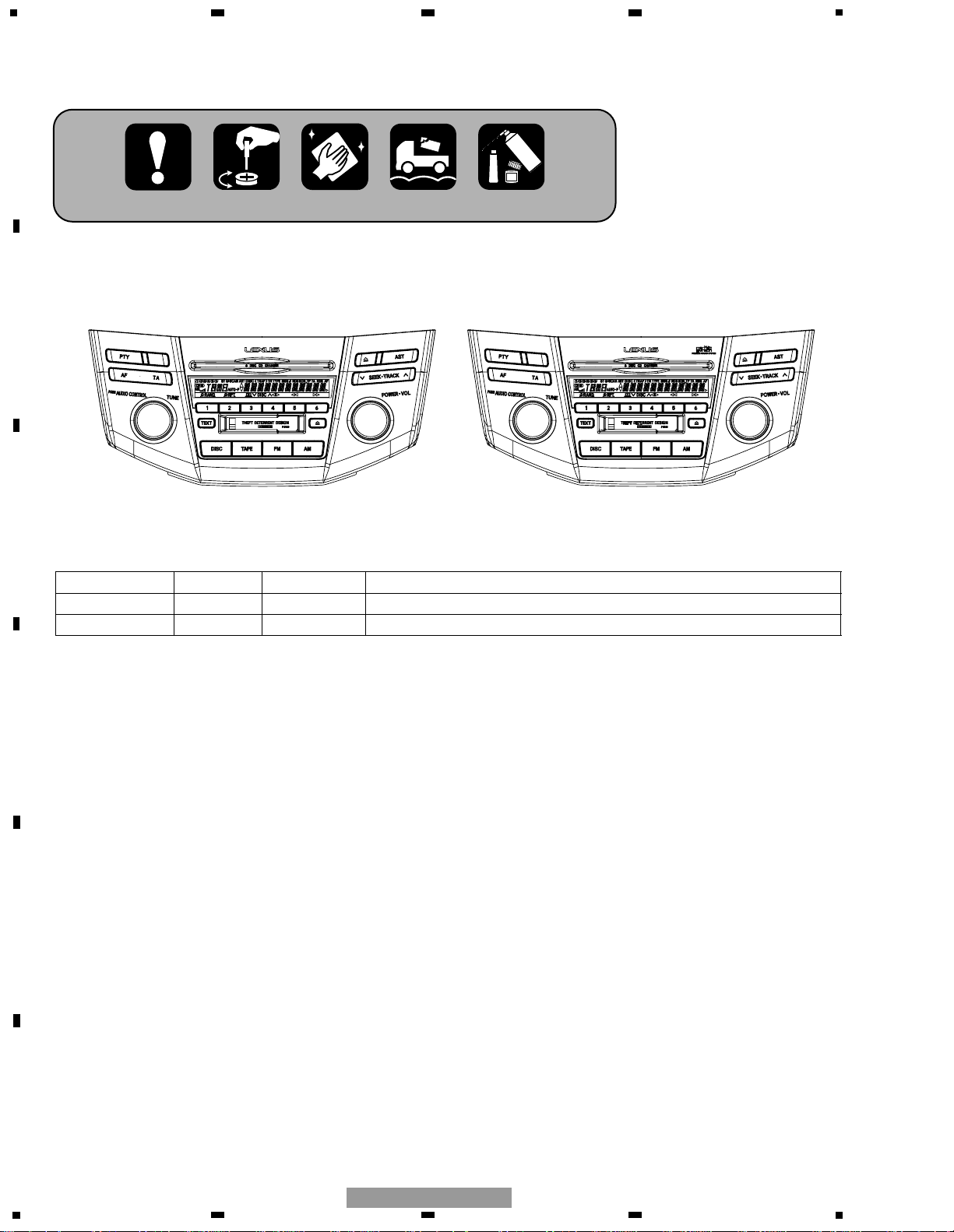
FX-MG8237ZT/EW
For details, refer to "Important symbols for good services".
FX-MG8237ZT/EW(P3920) FX-MG8337ZT/EW(P3921)
LOAD
LOAD
- This service manual should be used together with the following manual(s):
Model No. Order No. Mech. Module Remarks
CX-1011 CRT2406 3L Cassette Mech. Module:Mech.Description, Disassembly
CX-951 CRT2872 G2 CD Mech. Module:Circuit Description, Mech.Description, Disassembly
- Dolby noise reduction manufactured under license from Dolby Laboratories Licensing Corporation.
"Dolby" and the double-D symbol are trademarks of Dolby Laboratories Licensing Corporation.
Page 3
flashLAV
www.club-lexus.ru
3
5
6
7
8
F
E
D
C
B
A
5
6
7
8
FX-MG8237ZT/EW
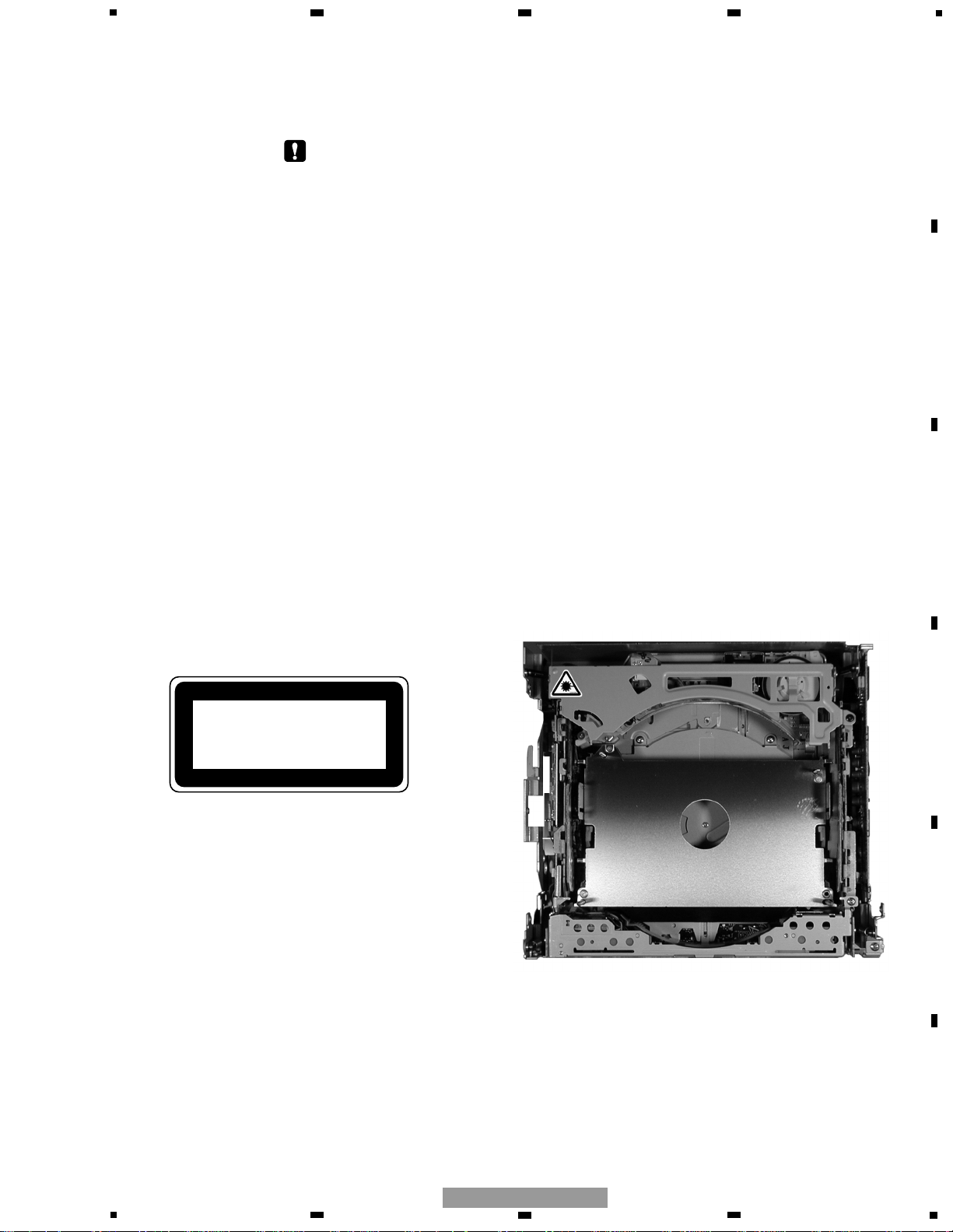
SAFETY INFORMATION
-
CD section precaution
1. Before disassembling the unit, be sure to turn off the
power. Unplugging and plugging the connectors during power-on mode may damage the ICs inside the
unit.
2. To protect the pickup unit from electrostatic discharge during servicing, take an appropriate treatment (shorting-solder) by referring to “the DISASSEMBLY” on page 83.
3. After replacing the pickup unit, be sure to check the
grating. (See p.73.)
This service manual is intended for qualified service technicians; it is not meant for the casual do-it-yourselfer.
Qualified technicians have the necessary test equipment and tools, and have been trained to properly and safely repair
complex products such as those covered by this manual.
Improperly performed repairs can adversely affect the safety and reliability of the product and may void the warranty.
If you are not qualified to perform the repair of this product properly and safely, you should not risk trying to do so
and refer the repair to a qualified service technician.
1. Safety Precautions for those who Service this Unit.
• When checking or adjusting the emitting power of the laser diode exercise caution in order to get safe, reliable
results.
Caution:
1. During repair or tests, minimum distance of 13cm from the focus lens must be kept.
2. During repair or tests, do not view laser beam for 10 seconds or longer.
2. A “CLASS 1 LASER PRODUCT” label is affixed to the
bottom of the player.
CLASS 1
LASER PRODUCT
4. Specifications of Laser Diode
Specifications of laser radiation fields to which human access is possible during service.
Wavelength = 800 nanometers
3. The triangular label is attached to the mechanism
unit frame.
Page 4
flashLAV
www.club-lexus.ru
4
1
234
12
34
F
E
D
C
B
A
FX-MG8237ZT/EW
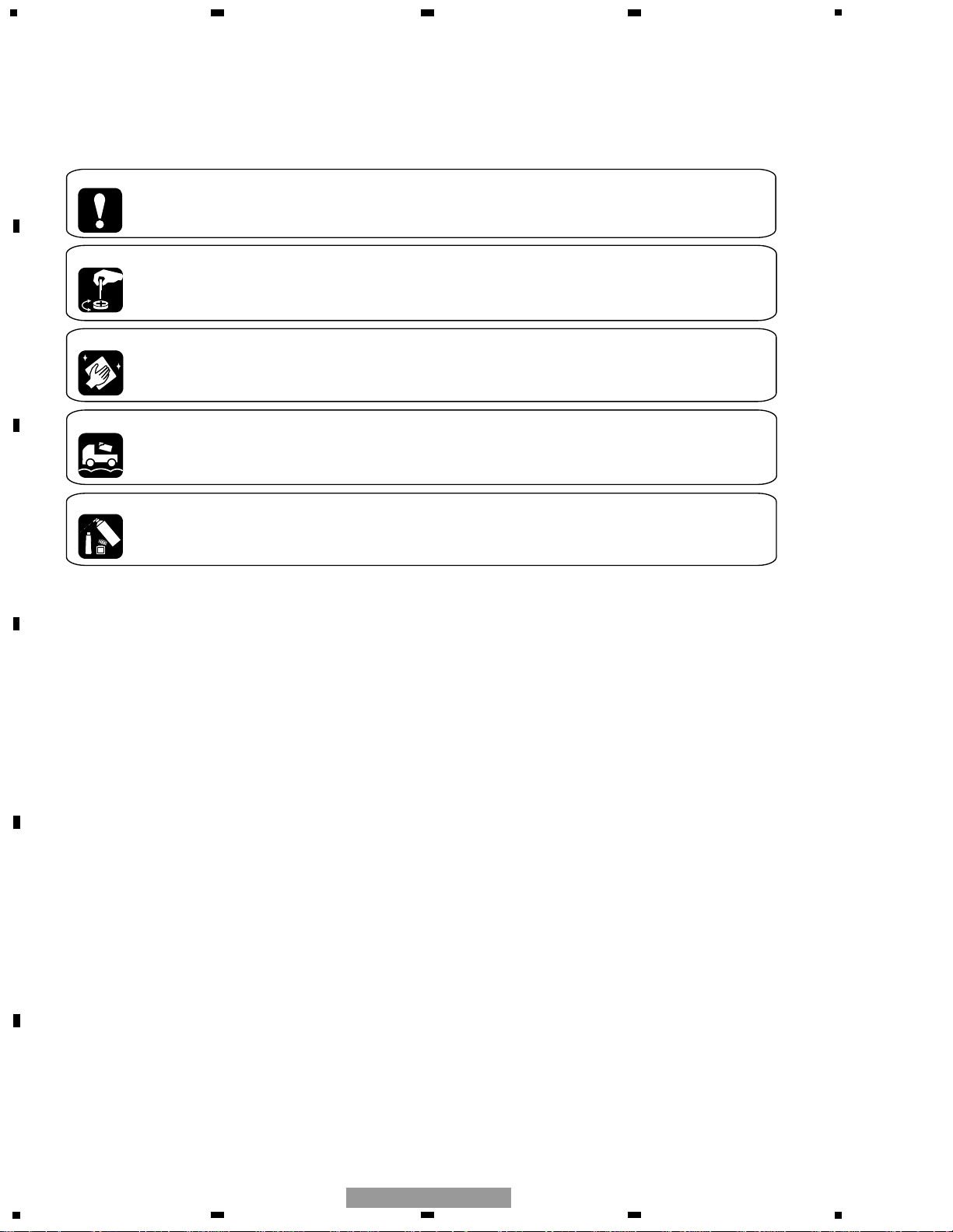
[ Important symbols for good services ]
In this manual, the symbols shown-below indicate that adjustments, settings or cleaning should be made securely.
When you find the procedures bearing any of the symbols, be sure to fulfill them:
2. Adjustments
To keep the original performances of the product, optimum adjustments or specification confirmation is indispensable.
In accordance with the procedures or instructions described in this manual, adjustments should be performed.
3. Cleaning
For optical pickups, tape-deck heads, lenses and mirrors used in projection monitors, and other parts requiring cleaning,
proper cleaning should be performed to restore their performances.
5. Lubricants, glues, and replacement parts
Appropriately applying grease or glue can maintain the product performances. But improper lubrication or applying
glue may lead to failures or troubles in the product. By following the instructions in this manual, be sure to apply the
prescribed grease or glue to proper portions by the appropriate amount.For replacement parts or tools, the prescribed
ones should be used.
4. Shipping mode and shipping screws
To protect the product from damages or failures that may be caused during transit, the shipping mode should be set or
the shipping screws should be installed before shipping out in accordance with this manual, if necessary.
1. Product safety
You should conform to the regulations governing the product (safety, radio and noise, and other regulations), and
should keep the safety during servicing by following the safety instructions described in this manual.
Page 5
flashLAV
www.club-lexus.ru
5
5
6
7
8
F
E
D
C
B
A
5
6
7
8
FX-MG8237ZT/EW
CONTENTS
SAFETY INFORMATION......................................................................................................................................................3
1. SPECIFICATIONS.................................................................................................................................................................6
2. EXPLODED VIEWS AND PARTS LIST ................................................................................................................................7
2.1 PACKING(FX-MG8237ZT-91/EW, FX-MG8337ZT-91/EW)............................................................................................7
2.2 EXTERIOR ......................................................................................................................................................................8
2.3 CD MECHANISM UNIT(1) ...........................................................................................................................................12
2.4 CD MECHANISM UNIT(2) ...........................................................................................................................................14
2.5 CASSETTE MECHANISM MODULE...........................................................................................................................16
3. BLOCK DIAGRAM AND SCHEMATIC DIAGRAM.............................................................................................................19
3.1 BLOCK DIAGRAM(1) ...................................................................................................................................................19
3.2 BLOCK DIAGRAM(2) ...................................................................................................................................................20
3.3 OVERALL CONNECTION DIAGRAM(GUIDE PAGE)..................................................................................................22
3.4 KEYBOARD UNIT.........................................................................................................................................................28
3.5 CD MECHANISM MODULE(GUIDE PAGE)................................................................................................................30
3.6 CASSETTE MECHANISM MODULE...........................................................................................................................40
4. PCB CONNECTION DIAGRAM..........................................................................................................................................42
4.1 MAIN UNIT...................................................................................................................................................................42
4.2 KEYBOARD PCB ..........................................................................................................................................................46
4.3 CD MECHANISM MODULE.........................................................................................................................................48
4.4 CASSETTE MECHANISM MODULE...........................................................................................................................54
4.5 RIGHT PCB, LEFT PCB.................................................................................................................................................56
5. ELECTRICAL PARTS LIST..................................................................................................................................................57
6. ADJUSTMENT ...................................................................................................................................................................66
6.1 CONNECTION DIAGRAM............................................................................................................................................66
6.2 AUDIO, TUNER ADJUSTMENT..................................................................................................................................68
6.3 TEST MODE .................................................................................................................................................................70
6.4 CD ADJUSTMENT.......................................................................................................................................................71
6.5 CHECKING THE GRATING AFTER CHANGING THE PICKUP UNIT.........................................................................73
6.6 TEST MODE(CD)..........................................................................................................................................................75
6.7 AVC-LAN DIAGNOSIS MODE.....................................................................................................................................79
7. GENERAL INFORMATION.................................................................................................................................................83
7.1 DIAGNOSIS..................................................................................................................................................................83
7.1.1 DISASSEMBLY..........................................................................................................................................................83
7.1.2 PCB LOCATIONS ......................................................................................................................................................88
7.1.3 CONNECTOR FUNCTION DESCRIPTION................................................................................................................89
7.2 PARTS...........................................................................................................................................................................90
7.2.1 IC................................................................................................................................................................................90
7.2.2 DISPLAY....................................................................................................................................................................97
7.3 EXPLANATION.............................................................................................................................................................98
7.3.1 SYSTEM BLOCK DIAGRAM.....................................................................................................................................98
7.3.2 OPERATIONAL FLOW CHART .................................................................................................................................99
7.4 NOTES ON SERVICING.............................................................................................................................................100
7.4.1 CLEANING...............................................................................................................................................................100
7.4.2 FACTORY SETTINGS..............................................................................................................................................100
8. OPERATIONS...................................................................................................................................................................101
Page 6

flashLAV
www.club-lexus.ru
6
1
234
12
34
F
E
D
C
B
A
FX-MG8237ZT/EW
1. SPECIFICATIONS
General
Power source................13.2V(10.5V–16.0V allowable) DC
Grounding system........................................Negative type
Backup current..............................................0.3mA or less
Dimensions............................320(W) x145(H) x175(D)mm
Weight..........................................................................2.8kg
Cassette player
Tape................................Compact cassette tape(C30-C90)
Tape speed ........4.76cm/sec.(+0.14cm/sec., -0.05cm/sec.)
Wow and flutter.................................0.2% or less(WRMS)
Crosstalk ..........................................................40dB or less
Stereo Separation.........................................30dB or more
S/N .................................................................40dB or more
Distortion.............................................................3% or less
CD player
System ...................................Compact disc audio system
Usable discs ..................................................Compact disc
Signal format .....................Sampling frequency : 44.1kHz
.....................................Number of quantization : 16;linear
S/N .................................................................65dB or more
Distortion..........................................................0.3% or less
FM tuner
Frequency range........................................87.5–108.0 MHz
S/N ..........................................46dB or more(54dBµ input)
Distortion..........................................................1.5% or less
IF interference ...............................................80dB or more
Image interference........................................35dB or more
Stereo Separation ..............................25dB or more(1kHz)
MW tuner
Frequency range ..........................................522–1,611 kHz
S/N 20dB useable sensibility........................34dBµ or less
S/N .................................................................42dB or more
Distortion..........................................................1.5% or less
IF interference ...............................................55dB or more
Image interference........................................45dB or more
LW tuner
Frequency range .............................................153–279 kHz
S/N 20dB useable sensibility........................40dBµ or less
S/N .................................................................42dB or more
Distortion..........................................................1.5% or less
IF interference ...............................................55dB or more
Image interference........................................45dB or more
Page 7
flashLAV
www.club-lexus.ru
7
5
6
7
8
F
E
D
C
B
A
5
6
7
8
FX-MG8237ZT/EW
2. EXPLODED VIEWS AND PARTS LIST
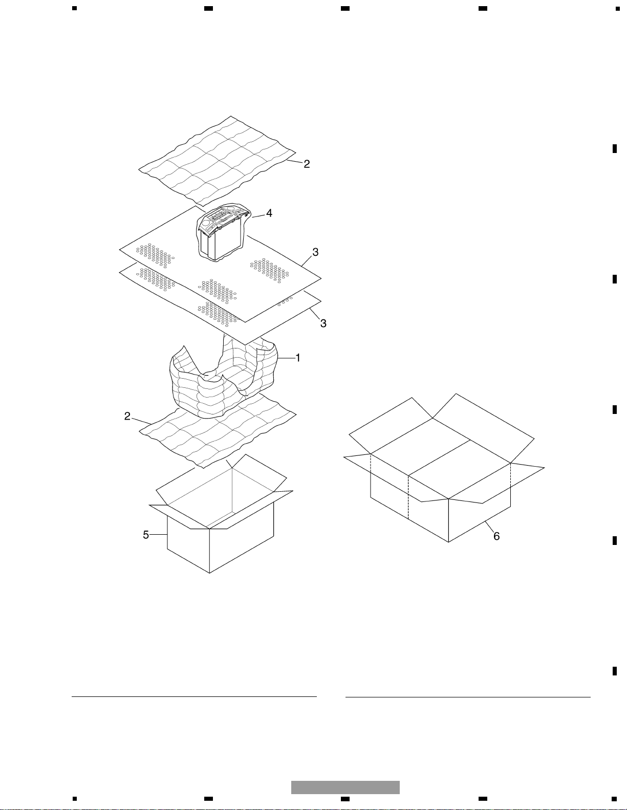
2.1 PACKING(FX-MG8237ZT-91/EW, FX-MG8337ZT-91/EW)
* 1 Air Cap CHW1945
* 2 Air Cap CHW1948
3 Cover CEG1045
4 Polyethylene Bag CEG1026
5 Carton CHG4861
6 Contain Box CHL4861
Mark No. Description Part No. Mark No. Description Part No.
NOTE:
- Parts marked by “*” are generally unavailable because they are not in our Master Spare Parts List.
- Screws adjacent to
∇ mark on the product are used for disassembly.
- For the applying amount of lubricants or glue, follow the instructions in this manual.
( In the case of no amount instructions, apply as you think it appropriate.)
- PACKING(FX-MG8237ZT-91/EW, FX-MG8337ZT-91/EW) SECTION PARTS LIST
Page 8
flashLAV
www.club-lexus.ru
8
1
234
12
34
F
E
D
C
B
A
FX-MG8237ZT/EW
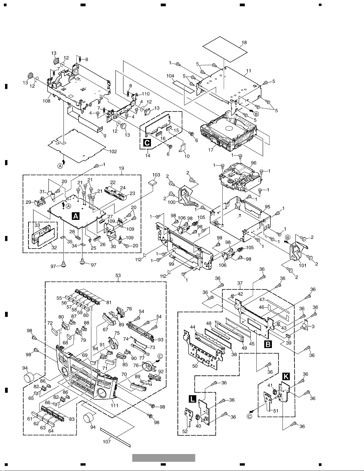
2.2 EXTERIOR
Page 9

flashLAV
www.club-lexus.ru
1 Screw BMZ26P040FTC
2 Screw
See Contrast table(2)
3 Connector CDE7260
4 Screw BMZ20P025FMC
5 Screw BMZ26P040FMC
6 Screw(M2x2.5) CBA1076
7 Spring CBH2481
8 Spring CBH2482
9 Connector CDE7020
10 Connector CDE7035
11 Case CNB2705
12 Sheet CNM5981
13 Damper CNV6608
14 Control Unit(G2T) CWX2649
15 Connector(CN601) CKS1956
16 Connector(CN101) CKS4512
17
Service Mechanism Assy(G2T) CXX1658
18 Label CRW1429
19 Main Unit
See Contrast table(2)
20 Screw BMZ30P060FTC
21 Screw(M3x6) CBA1393
22 Connector(CN801) CKM1322
23 Connector(CN473) CKM1350
24 Connector(CN472) CKM1351
25 Plug(CN354) CKS-291
26 Connector(CN353) CKS3568
27 Connector(CN351) CKS3886
28 Connector(CN804) CKS4361
29 Connector(CN501) CKX1064
30 Holder CNC9639
31 Holder CNC9701
32 FM/AM Tuner Unit CWE1633
33 Holder CNC8855
34 Terminal(CN802) VNF1084
35 Terminal(CN803) VNF1084
36 Screw BPZ20P080FTC
37 Keyboard Unit CWS1363
38 LCD(LCD901) CAW1722
39 Connector(CN901) CKS4361
40 Connector(CN904) CKS4591
41 Connector(CN905) CKS4591
42 Connector(CN902) CKS4592
43 Connector(CN903) CKS4592
44 Holder CND1021
45 Sheet CNM7958
46 Seal CNM7970
47 Seal CNM7971
48 Connector CNV7249
49 Lighting Conductor CNV7250
50 Rubber CNV7323
51 Rubber CNV7324
52 Rubber CNV7325
53 Grille Assy
See Contrast table(2)
54 Screw BPZ20P080FTC
55 Button(1) CAC7599
56 Button(2) CAC7600
57 Button(3) CAC7601
58 Button(4) CAC7602
59 Button(5) CAC7603
60 Button(6) CAC7604
61 Button(DISC) CAC7620
62 Button(TAPE) CAC7621
63 Button(FM) CAC7622
64 Button(AM) CAC7623
65 Button(TEXT) CAC7624
66 Button(TAPE EJECT) CAC7625
67 Button(AF,TA) CAC7627
68 Button(LOAD) CAC7629
69 Button(CD EJECT) CAC7628
70 Button(SEEK,TRACK) CAC7626
71 Button(AST) CAC7630
72 Button(PTY) CAC7631
73 Door
See Contrast table(2)
74 Spring CBH2663
75 Lighting Conductor CNV7251
76 Lighting Conductor CNV7252
77 Lighting Conductor CNV7253
78 Holder CNV7256
79 Holder CNV7257
80 Holder CNV7258
81 Holder CNV7259
82 Holder CNV7260
83 Holder CNV7261
84 Holder CNV7316
85 Holder CNV7317
86 Lighting Conductor CNV7319
87 Lighting Conductor CNV7320
88 Lighting Conductor CNV7321
89 Lighting Conductor CNV7330
90 Lighting Conductor CNV7467
91 Lighting Conductor CNV7469
92 Holder CNV7472
93 Door Assy CXB9033
94 Knob Unit CXB8884
95 Chassis Unit CXB9795
96
Cassette Mechanism Module EXK4295
97 Screw IMS26P040FTC
98 Screw IMS26P060FTC
99 Frame CND1789
100 86211-48030-A
See Contrast table(2)
101 86212-48030-A See Contrast table(2)
102 Insulator CNM7496
103 Spacer CNM8078
104 Seal CNM8343
105 90467-10203 CNV5641
106 Guide CNV7306
107 Label CRW1425
108 Chassis Unit CXA8029
109 Transistor(Q809,811,812) 2SB1185
110 Bracket Unit CXB8082
111 Grille Unit
See Contrast table(2)
112 Sheet CNM8435
9
5
6
7
8
F
E
D
C
B
A
5
6
7
8
FX-MG8237ZT/EW
Mark No. Description Part No. Mark No. Description Part No.
(1) EXTERIOR SECTION PARTS LIST
Page 10
flashLAV
www.club-lexus.ru
10
1
234
12
34
F
E
D
C
B
A
FX-MG8237ZT/EW
Part No.
Mark No. Symbol and Description FX-MG8237ZT/EW FX-MG8337ZT/EW
2 Screw BMZ50P080FTC BMZ50P080FTC
19 Main Unit CWM8388 CWM8556
53 Grille Assy CXC2067 CXC2068
73 Door CAT2354 CAT2355
100 86211-48030-A CND1247 CND1247
101 86212-48030-A CND1248 CND1248
111 Grille Unit CXB9904 CXB9905
Part No.
Mark No. Symbol and Description FX-MG8237ZT-91/EW FX-MG8337ZT-91/EW
2 Screw Not used Not used
19 Main Unit CWM8388 CWM8556
53 Grille Assy CXC2067 CXC2068
73 Door CAT2354 CAT2355
100 86211-48030-A Not used Not used
101 86212-48030-A Not used Not used
111 Grille Unit CXB9904 CXB9905
(2) CONTRAST TABLE
FX-MG8237ZT/EW, FX-MG8337ZT/EW, FX-MG8237ZT-91/EW and FX-MG8337ZT-91/EW are constructed
the same except for the following:
Page 11

flashLAV
www.club-lexus.ru
11
5
6
7
8
F
E
D
C
B
A
5
6
7
8
FX-MG8237ZT/EW
Page 12
flashLAV
www.club-lexus.ru
12
1
234
12
34
F
E
D
C
B
A
FX-MG8237ZT/EW
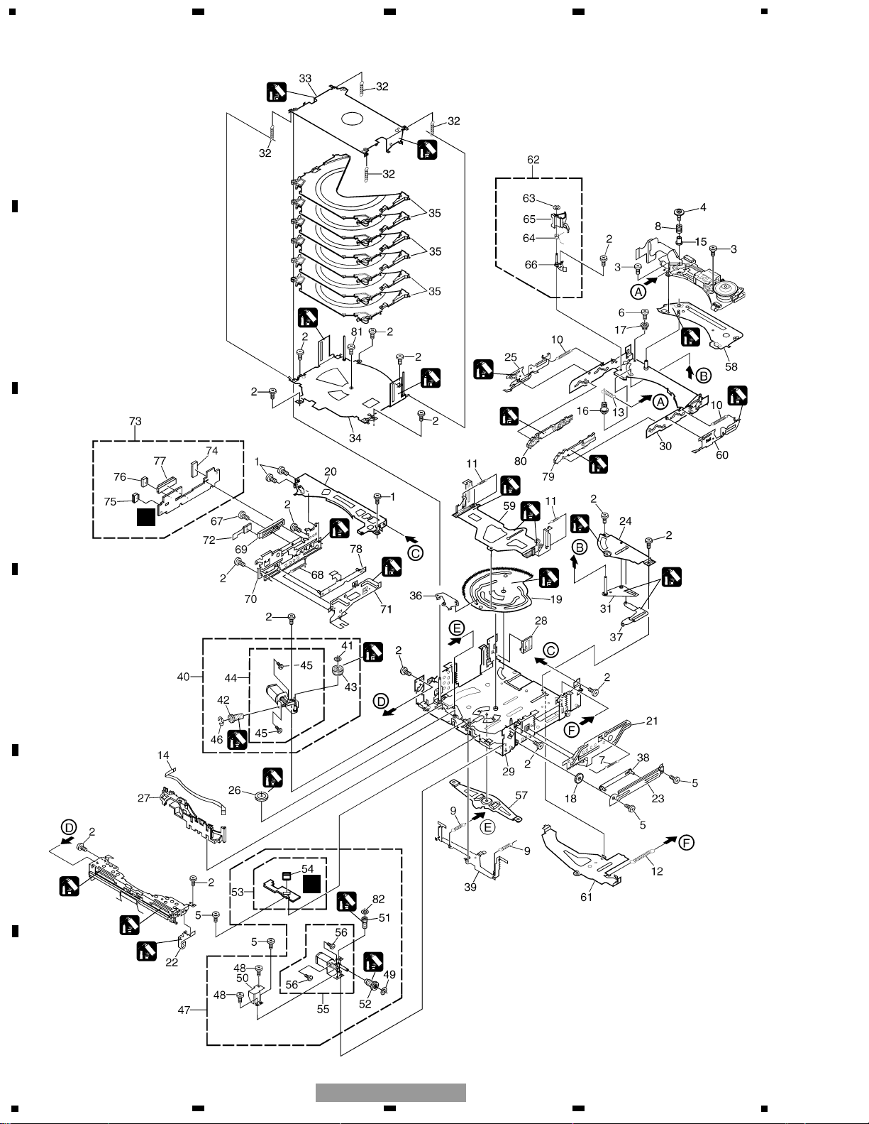
2.3 CD MECHANISM UNIT(1)
1
1
1
3
3
1
3
1
1
3
3
3
F
3
3
3
1
1
1
3
1
1
3
D
2
1
1:GEM1043
2:GEM1042
3:GEM1024
Page 13

flashLAV
www.club-lexus.ru
13
5
6
7
8
F
E
D
C
B
A
5
6
7
8
FX-MG8237ZT/EW
Mark No. Description Part No. Mark No. Description Part No.
1 Screw BMZ20P020FZB
2 Screw BMZ20P025FTC
3 Screw(M2x2) CBA1556
4 Screw(M2x2.5) CBA1626
5 Screw(M2x2.5) CBA1609
6 Screw(M2x4.5) CBA1629
7 Spring CBH2460
8 Spring CBH2461
9 Spring CBH2484
10 Spring CBH2694
11 Spring CBH2486
12 Spring CBH2487
13 Spring CBH2500
14 Connector CDE6698
15 Collar CLA4329
16 Collar CLA4330
17 Collar CLA4331
18 Gear CND1649
19 Cam Gear CND1650
20 Frame CND1651
21 Steer CND1667
22 Arm CND1657
23 Bracket CND1658
24 Bracket CND1660
* 25 Lever CNC9953
26 Gear CNV6612
27 Holder CNV6648
28 Holder CNV6738
* 29 Chassis Unit CXC1642
* 30 Frame Unit CXC1643
* 31 Arm Unit CXC1647
32 Spring CBH2488
33 Holder Unit CXC1644
34 Holder Unit CXC1646
35 Tray Unit CXB6930
36 Lever Unit CXC1648
* 37 Lever Unit CXC1649
38 Lever Unit CXC1650
* 39 Lever Unit CXC1651
40 Cam Motor Assy CXB7522
41 Washer CBF1064
42 Gear CNV6610
43 Gear CNV6611
44 Motor Unit(-A)(M1) CXC1144
45 Screw JFZ20P020FTC
46 Washer YE20FTC
47 ELV Motor Assy CXB7523
48 Screw BMZ20P025FTC
49 Washer CBF1064
50 Holder CND1668
51 Gear CNV6634
52 Gear CNV6635
53 PCB Unit(LED) CWX2614
* 54 Connector(CN31) CKS4523
55 Motor Unit(-A)(M2) CXC1145
56 Screw JFZ20P020FTC
* 57 Arm Unit CXC1653
58 Bracket Unit CXC1654
* 59 Lever Unit CXC1658
* 60 Lever Unit CXC1659
* 61 Lever Unit CXC1661
62 Arm Assy CXB8822
63 Washer CBF1038
64 Spring CBH2489
65 Arm CNV6735
66 Bracket Unit CXC1652
67 Screw BMZ20P025FTC
68 Spring CBH2459
69 Volume(VR1) CCW1023
70 Bracket CND1652
71 Steer CND1656
72 Flexible PCB CNP6368
73 PCB Unit(SIDE) CWX2613
74 Connector(CN12) CKS3991
* 75 Connector(CN14) CKS4404
76 Connector(CN13) CKS4525
77 Connector(CN11) CKS4572
78 Lever Unit CXC1645
* 79 Lever Unit CXB9121
* 80 Lever Unit CXB9122
81 Screw JFZ20P020FTC
82 Washer CBF1037
- CD MECHANISM UNIT(1) SECTION PARTS LIST
Page 14
flashLAV
www.club-lexus.ru
14
1
234
12
34
F
E
D
C
B
A
FX-MG8237ZT/EW
2
1
1
1
1
1
1
1
1
1:GEM1043
2:GEM1042
G
H
E
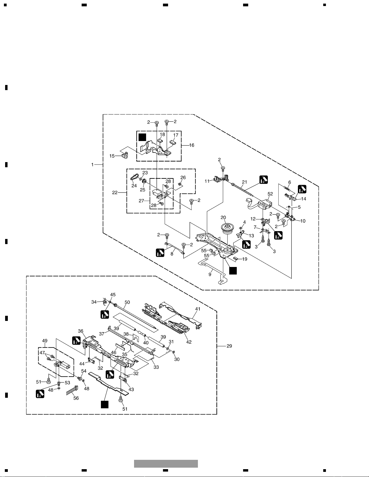
2.4 CD MECHANISM UNIT(2)
Page 15

flashLAV
www.club-lexus.ru
15
5
6
7
8
F
E
D
C
B
A
5
6
7
8
FX-MG8237ZT/EW
Mark No. Description Part No. Mark No. Description Part No.
1 Carriage Mech. Assy(G2T) CXB8842
2 Screw(M2x2) CBA1556
3 Screw(M2x6) CBA1628
4 Washer CBF1038
5 Spring CBH2453
6 Spring CBH2480
7 Spring CBL1521
* 8 Guide CNC9402
9 Flexible PCB CNP6217
10 Holder CNV6624
11 Holder CNV6625
12 Rack CNV6642
13 Arm CNV6731
14 Lever CNV6736
15 Holder CNV6737
16 PCB Unit CWX2611
17 Connector(CN41) CKS3785
18 Connector(CN42) CKS4508
19 Connector(CN1) CKS4508
20 Support Wheel Unit CXC1768
21 Screw Unit(-B) CXB7518
22 Carriage Motor Assy CXB7521
23 Washer CBF1038
24 Belt CNT1088
25 Pulley CNV6627
26 Gear CNV6629
27 Motor Unit(-A)(M3) CXC1143
28 Screw JFZ14P020FTC
29 Loading Mech. Assy CXB7525
30 Washer CBF1037
* 31 Washer CBF1075
* 32 Spring CBH2450
33 Spring CBH2452
* 34 Spring CBH2457
* 35 Spring CBH2580
* 36 Frame CND1653
* 37 Arm CND1654
* 38 Sheet CNM7295
39 Roller CNV6616
40 Collar CNV6617
* 41 Guide CNV6622
* 42 Holder CNV6636
* 43 Lever CNV6732
* 44 Lever CNV6733
45 Collar CNV6734
* 46 Holder CNV7144
47 Screw JFZ12P018FTC
48 Washer CBF1037
* 49 Motor Unit(-A) CXC1146
50 Shaft Unit(-C) CXB7528
51 Screw JFZ20P020FTC
52 PU Unit(PX1)(Service) CXX1569
* 53 Gear CNV6620
* 54 Gear CNV6621
55 Switch(S1,2) CSN1057
* 56 Connector CDE6674
- CD MECHANISM UNIT(2) SECTION PARTS LIST
Page 16
flashLAV
www.club-lexus.ru
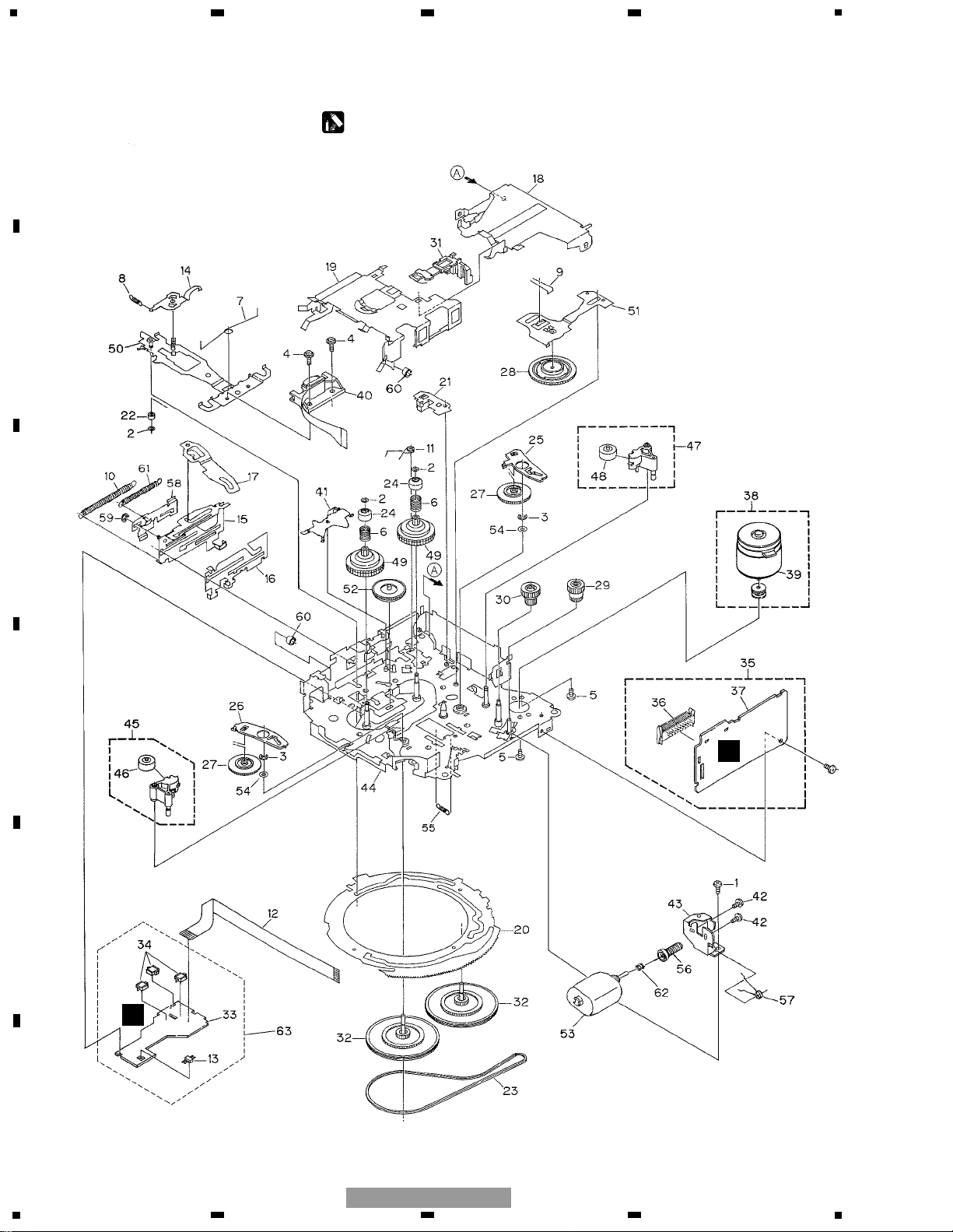
2.5 CASSETTE MECHANISM MODULE
16
1
234
12
34
F
E
D
C
B
A
FX-MG8237ZT/EW
I
J
For grease application, refer to the service manual for CX-1011 (CRT2406)
Page 17

flashLAV
www.club-lexus.ru
17
5
6
7
8
F
E
D
C
B
A
5
6
7
8
FX-MG8237ZT/EW
- CASSETTE MECHANISM MODULE SECTION PARTS LIST
1 Screw BSZ20P040FMC
2 Washer CBF1037
3 Washer CBG1003
4 Screw EBA1028
5 Screw CBA1037
6 Spring EBH1653
7 Spring EBH1642
8 Spring EBH1641
9 Spring EBH1626
10 Spring EBH1627
11 Spring EBH1648
12 Cord EDD1024
13 Photo-reflector(Q101) EGN1004
14 Arm ENC1526
15 Lever Unit EXA1610
16 Lever ENC1543
17 Arm ENC1532
18 Frame ENC1533
19 Holder ENC1547
20 Gear ENC1535
21 Arm ENC1550
22 Roller ENR1040
23 Belt ENT1027
24 Collar ENV1508
25 Arm ENV1539
26 Arm ENV1540
27 Gear ENV1569
28 Gear ENV1547
29 Gear ENR1044
30 Worm Wheel ENV1559
31 Lever ENV1551
32 Flywheel ENV1554
33 Gathering PCB ENX1073
34 Switch(S101,S102,S103) ESG1007
35 Deck Unit EWM1043
36 Plug(CN251) CKS3540
37 Gathering PCB ENX1076
38 Motor Unit(M1) EXA1618
39 Motor EXM1035
40 Head Assy(HD1) EXA1594
41 Arm ENC1537
42 Screw JGZ20P025FNI
43 Bracket ENC1559
44 Chassis Unit EXA1636
45 Pinch Holder Unit EXA1608
46 Pinch Roller ENV1518
47 Pinch Holder Unit EXA1607
48 Pinch Roller ENV1518
49 Reel Unit EXA1625
50 Head Base Unit EXA1611
51 Lever Unit EXA1587
52 Gear Unit EXA1596
53 Motor Unit(M2) EXA1623
54 Washer HBF-179
55 Spring EBH1537
56 Worm Gear ENV1564
57 Spring EBH1655
58 Lever ENC1548
59 Washer YE15FUC
60 Tube ENM1039
61 Spring EBH1645
62 Spring EBH1545
63 Sensor Unit EWM1041
Mark No. Description Part No. Mark No. Description Part No.
Page 18

flashLAV
www.club-lexus.ru
18
1
234
12
34
F
E
D
C
B
A
FX-MG8237ZT/EW
Page 19
flashLAV
www.club-lexus.ru
19
5
6
7
8
F
E
D
C
B
A
5
6
7
8
FX-MG8237ZT/EW
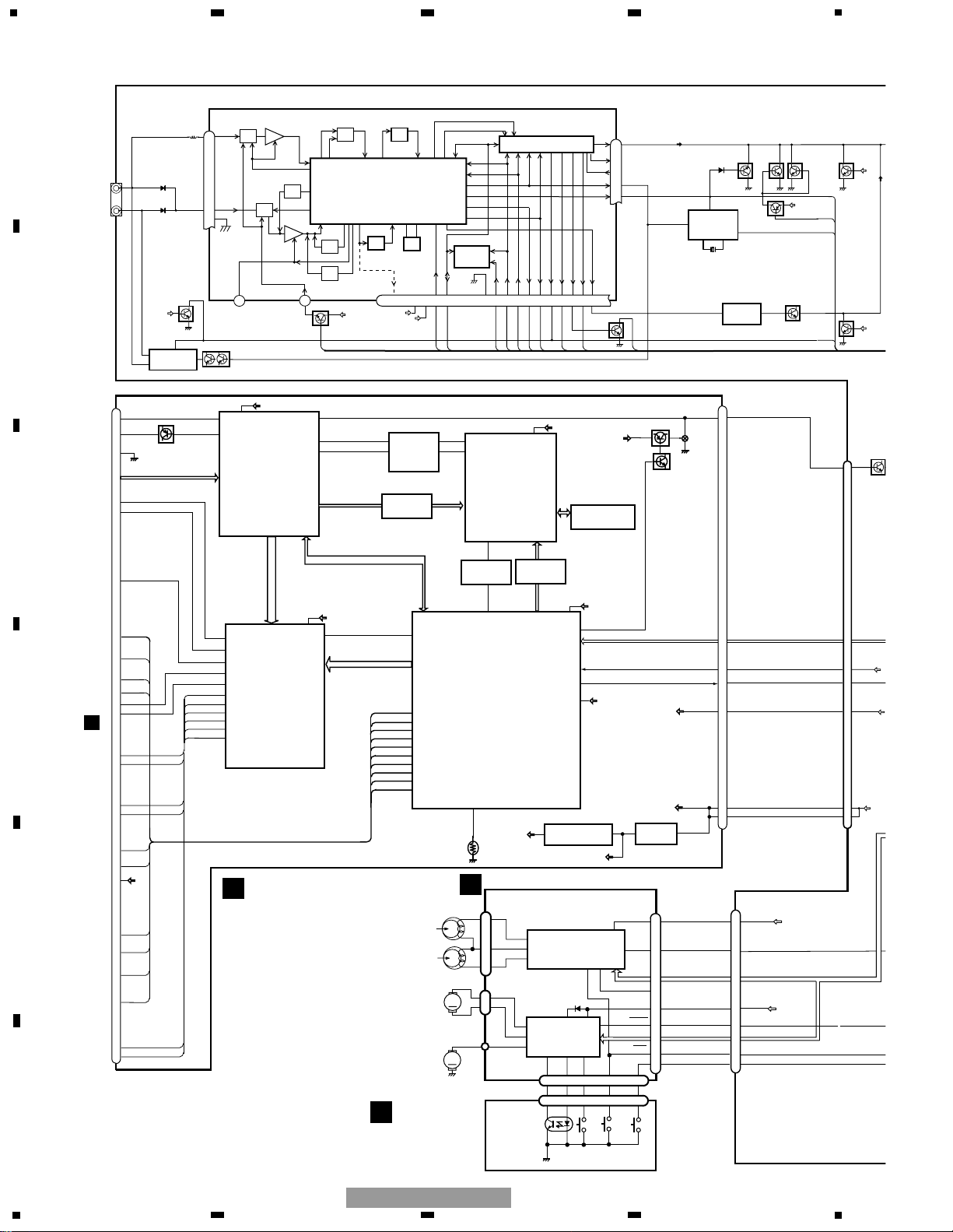
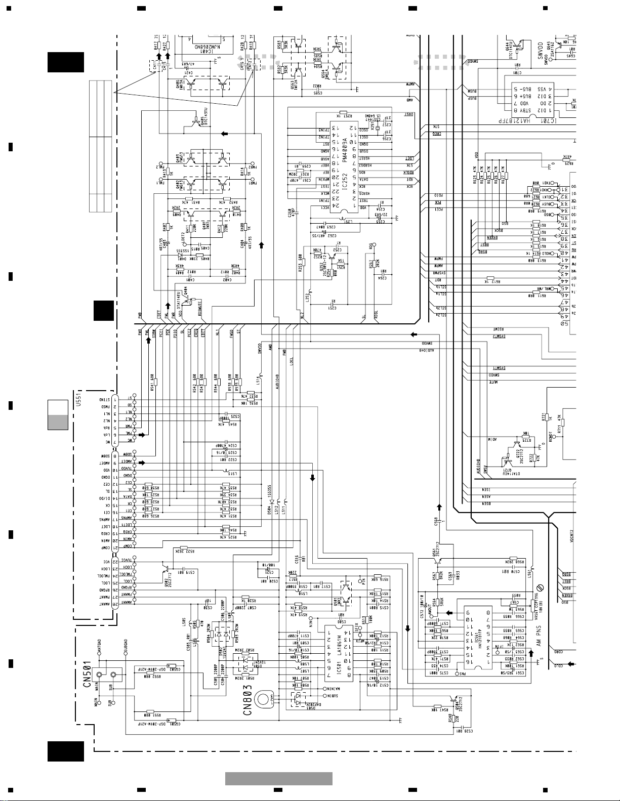
3. BLOCK DIAGRAM AND SCHEMATIC DIAGRAM
3.1 BLOCK DIAGRAM(1)
M
LOADING
VR1 ELV SENSE
VR11
S31 CAMLOAD
PU UNIT(SERVICE)(PX1)
PCB UNIT(M2 UNIT)
HOLOGRAM
UNIT
FOCUS ACT
TRACKING ACT
MD
LD+
LD-
LD
MD
FO+
TO+
CN41
M
M
SPINDLE
M3 CARRIAGE
CLAMP
10
2
1
16
14
A+C,B+D,
E,F
2
A3
3
5
A2
A1
IC 1
BA6849FS
MOTOR
DRIVER
CN1
EC
19
S2 CLAMP
HOME
S1 HOME
5
2
1
5
2
1
CN42
S41 LOAD3
PCB UNIT
23
14
13
28
26
6
9
10
1
11
12
23
14
13
28
26
6
9
10
1
11
12
PCB UNIT(SIDE)
CN12
S11 CAMCLMP
M
M1 CAMGEAR
CN31
M
M2 ELV
S32 CAMEOK
D31
D32
PCB UNIT
(LED)
CN14
CN13
Q22 Q21
S21 LOAD1
S22 LOAD2
PCB UNIT
(LOAD)
2
1
4
5
CN11
MD
23
32
33
LD+
LD-
FOP
18
TOP
20
SIN(EC)
40
CLAMP
36
HOME
37
LOADSW2
45
50
COP
34
COM
35
CGM
3
CGP
1
ELP
15
ELM
13
CAMOK
11
CAMLOAD
10
LED
12
ELVSNS
46
EREF
48
LOADPHT
7
LOADSW1
8
LOP
6
LOM
5
G
F
H
D
E
1
1
2
2
5
5
7
7
8
8
C
CN101
Page 20
flashLAV
www.club-lexus.ru
20
VDCNT2
R
CN501
SUB
ANTENNA
16
13
10
11
2
AUDIO+B
SWVDD
MAIN
ANTENNA
IC 501
LA1061M
5
6
Q501
DIVERSITY
COMP
IC561
HA12181FP
AM NOISE CANCELER
CN351
SUB
MAIN
1
NIN
39
FMSD
FML
Q401
MFIX
13
CSL
BU
8
4
19
20
3
CN353
IC 3
EEPROM
28
27
FM/AM 1ST IF 10.7MHz
T51 Q51 CF51
CF52 CF53
IC1
MIXER, IF AMP, DET.
6
21
18
LDET
COMP
222510 14 12 15 16 8 13 2 3 4
CF202
VDD
VCC
DI/DO
CE2CKCE1
SDBWSLFMSD
NL1
NL2
IC 2 FM MPX
AMANT
FMANT
ATT
ATT
AMRF
FMRF
IMG ADJ
RF ADJ
X901
10.25MHz
ANT ADJ
LOCL
23
LOCH
AMDET
MPXREF 41kHz
AM 2ND IF
450kHz
19
CREQ
11
DGND
1
STIND
L ch
5
R ch
924
AMDET
FMLOCL
20
177
AMPNS
WC
26
RFGND
AMIN
Q561
IC252
PM4009A
X251
RDS
DECODER
1211
20
8
AM
Q402
VDD
Q404
Q351
LDET
RDSMUTE
FMSD
1
CD9V
11
AUDIO+B
RDT
5
Q403
Q406
AMB
Q405
FMB
Q252
NL2
Q502
AUDIO+B
LOCL
Q504
SWVDD
STBY
B.U
MUTE
MTL
LOAD
5
1
4
2
1
3
4
11
9
20
19
8
I
DECK UNIT
IC251
HA12216F
IC351
PA2020A
EQ AMP
MECHANISM
DRIVER
CN251
CN252
CN254
CN255
CN253
6
16
TAPE+B
Lch
10
12
FWD
L-ch
REV
L-ch
37
38
39
18
19
17
3
15 6
8
7
10
CN256
3
15 6
S101
LOAD
S102
MODE
Q101
REEL
SENSE
M
M
M2
SUB
MOTOR
M1
MAIN
MOTOR
5
2
1
SENSOR UNIT
S103
70µs
4
4
J
I
23
32
33
18
20
40
36
37
45
50
34
35
3
1
15
13
11
10
12
46
48
7
8
6
5
CONTROL UNIT(G2T)
Q101
96
PD
CD CONTROL
97
LD
A+C,B+D,E,F
L-OUT
16
IC504(1/2)
TC74VHCT08AFT
3 1,2
IC 201
UPD63711GC
6 4,5
33
LRCKIN
31
SCKIN
3.3V - 5V CONVERTER
5V - 3.3V CONVERTER
IC505(1/2)
TC74VHC541FT
DOUT,LRCK,
SCKO,RADV,
SBSY
15
ZLRCK
14
ZSCK
IC501
SM5903BFP
SHOCK PROOF
CONTROLLER
10
V+5
22
3V
IC507
MSM51V17400F6TFT
IC702
PD5748E
MECH.
CONTROLLER
IC504(2/2)
TC74VHCT08AFT
IC505(2/2)
TC74VHC541FT
YMDATA,
YMLD,
YMCLK
21
ZSENSE
9,10
8
98
ZSENSE
BUFFER RAM
14
VDD
VCC2
3+3ch
DRIVER
IC 301
BD7962FM
ELV1,ELV2,ELVCONT,LD1,LD2,
LOCONT,CG1,CG2
9
29
CONT
MUTE
MOTOR CONTROL
14
VD
XSI,XSO,XSCK,XSTB,XAO,XRST,FOK,LOCK,
TSI,TSO,TSCK,TSTB,PACK,SBSY
SERVO DSP I/F
SERVO EQUALIZER OUTPUT
FD,TD,SD,MD
18
15
OUT1+
OUT2-
Q602
Q603
CD MUTE
VD
Q601
74
CDMUTE
CN101
CN501
BSI,BSO,BSCK,BRXEN,BSRQ,BRST
10
reset
LOUT
37
VDCONT
9
6
3
RESET
VDCONT
VDD
VD
VD
17
18
IC 303
BA05SFP
5V REGULATOR
4
2
V+5
S-818A33AUC-BGN
3V REGULATOR
1
5
IC 302
3V
92
TEMP
94
VDIN
VD
26
OPOUT
COP
COM
ELP
ELM
LOP
LOM
CGM
CGP
19
20
2
3
21
22
34
35
OUT3+
OUT3-
OUT5OUT5+
OUT4+
OUT4OUT6+
OUT6-
VD
CLAMP
HOME
LOADSW2
CAMCLMP
ELVSNS
EREF
72
79
82
23
91
92
HOME2
HOME
LOADSW2
CAMCLMP
EREFF
CAMOK
21
CAMOK
CAMLOAD
22
CAMLOAD
LOADPHT
89
LOADPHT
LOADSW1
81
LOADSW1
ELVSENS
C
F
CN11
8
FM/AM TUNER UNIT
1
234
12
34
F
E
D
C
B
A
FX-MG8237ZT/EW
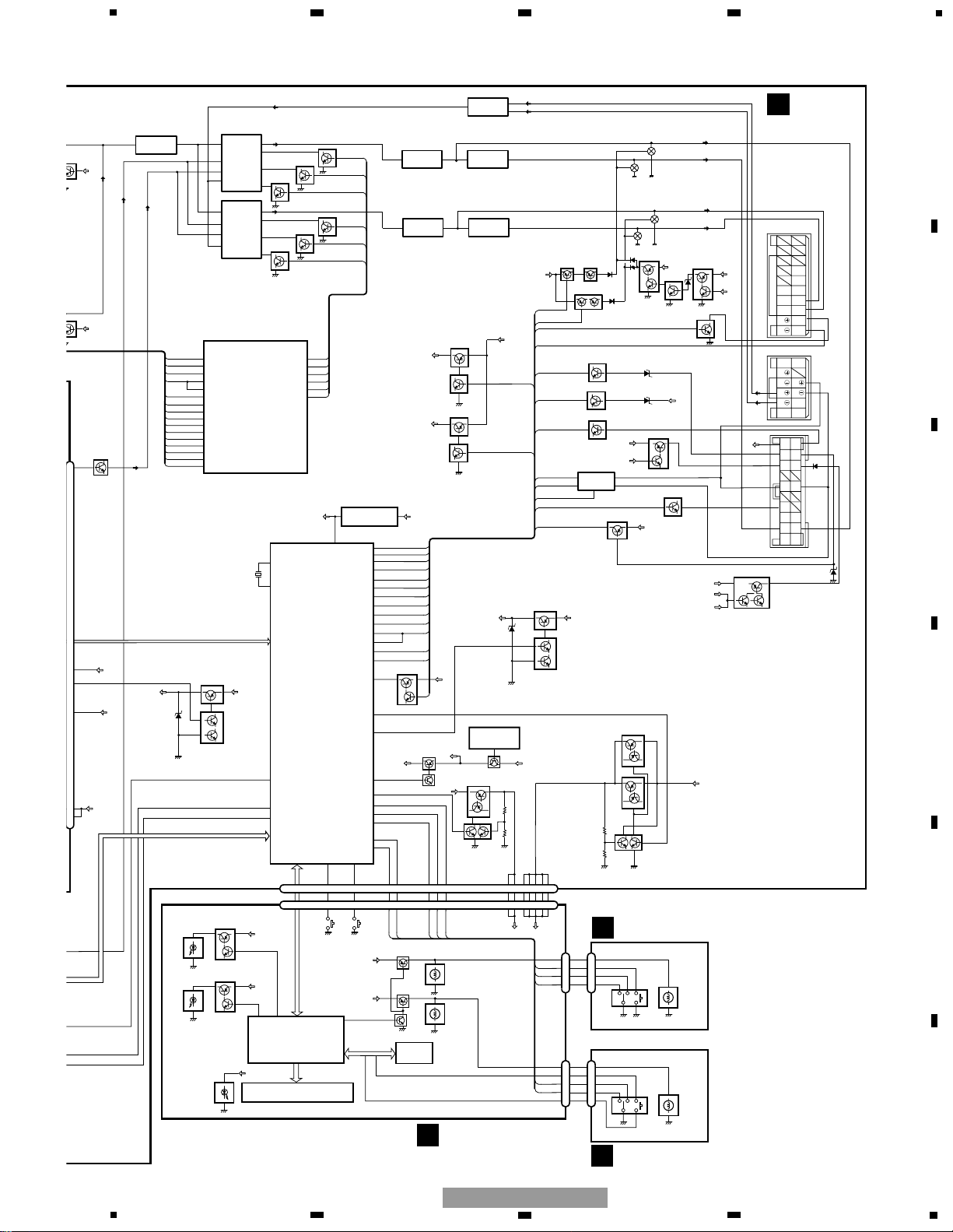
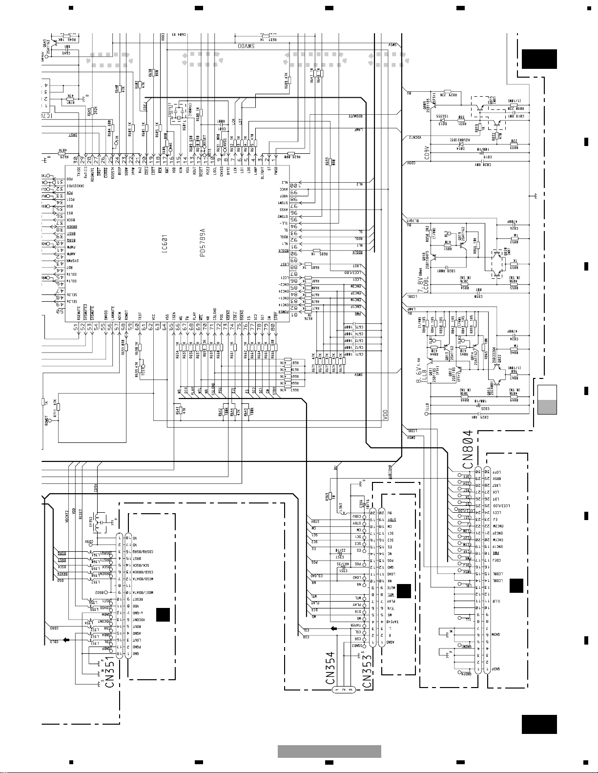
3.2 BLOCK DIAGRAM(2)
Page 21
flashLAV
www.club-lexus.ru
21
13
XOUT
X601
VDCNT2
17 23
17
20 74
23 21 22
19
21 22
19
20
LC75804W
IC 901
LCD901
20
14,15
14,1599
CD
EJECT
TAPE
EJECT
VDD
IC 602
S-80835CNUA-B8U
53
12
12
RESET
RESET
RESET
15
XIN
13
XOUT
RESET
75
73
28
BLIGHT
83
82
ENC1+
85
ENC2-
84
ENC2+
65
CONTROLLER
SYSTEM
IC 601(2/2)
KEY
MATRIX
CN804
CN902
VDD
KEYBOARD PCB
ENC2P
ENC2M
ENC1P
pwr
LCDBL
ILLB
cdej
csej
asens
bsens
Q818
Q819
BU
Q816
Q808
KEY CONTROLLER
LCD DRIVER
16
13
10
11
2
VR902
POWER•VOL
VR901
AUDIO CONTROL•TUNE
ENC1-
power
81
18
18
ENC1M
ILLB
101011
11
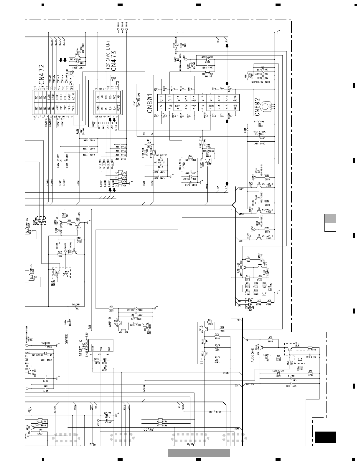
AVC-LAN BUS DRIVER
UNBALANCE TO BALANCE CONVERTER
IC701
HA12187FP
6
BU
AVC-LAN MUTE
Q801
ISENS
Q805
BSENS
Q806
ASENS
Q807
5
Q812
Q814
4
LAMP
Q802
Q809
Q815
CD9V
AUDIO+B
VDCONT2
SYSPWR
Q865
Q867
IC401
NJM2068MD
TUNER
MIXING AMP
1
IC203
NJM2068MD
67
IC204
NJM2068MD
67
Q864
Q205
sysmute
30
29
21
TX
RX1
RX2
isens
22
IPPW
1
2
8
bsens
TX
RX
isens
IPPW
MUTE
RX
56
LANMUTE
CN351
Q811
Q813
BU
AUDIO +B REGULATOR
CD 9V REGULATOR
BU
Q563(1/2)
Q564(1/2)
Q563(2/2)
Q564(2/2)
AUDIO+B
FMB
AMB
42
AMPW
41
FMPW
FML
CSL
CDL
B
SWVDD
IC202
TC4052BF
IC302
TC4052BF
2
2
3
1
1
4
4
BALANCE TO UNBALANCE CONVERTER
IC303
NJM2068MD
67
IC304
NJM2068MD
67
3
ACC+B
R
L
R
SGND
mute
GND
TX
BU+B
TX
L
CN473
SW2
SW1
TX1
TX1
GND
ADIM
SLD1
CN472
RSR+
RSR-
RSL+
RSL-
rmut
ACC
+B
ILL-
ILL
ANT
AMP
TX-
TX+
mute
R-
R+
L-
L+
GND
SLD
CN801
Q351
Q204
Q305
Q304
IC870
S-812C56AUA-C3K
3
VDD
VDD5V REGULATOR
BU
Q870
1
1
CD9V
UNBALANCE TO BALANCE CONVERTER
SELECTOR
SELECTOR
IC201
NJM2068MD
7
5
5
5
LANL
Q866
52
sysmute@
asens
Q451
Q452
Q453
AMB
FMB
ANT+B
Q645
SWVDD
Q644
55
SWVDD
43
SYSPWR
CONTROLLER
IC 601(1/2)
SYSTEM
FMSD
RDSMUTE
LDET
DI/DO
CE2
CK
CE1
SL
1
FMSD
3
RDSMUTE
19
ldet
32
PDI
11
PDO
33
PCE2
34
pck
93
PCE1
31
SL
MAIN UNIT
A
PD5789A
PD5789A
80
stby
69
mtl
71
CSLOAD
RDT
44
RDT
BU
ADIM
Q721
Q722
57
ADIM
SW5V
ADIM
1
2
6
7
1
2
6
7
ILLCONT
Q901
Q902
Q903
ILLB
ILLB
Q907
Q908
ILLB
Q905
Q906
ILLB
34
CDILLRCDILLG
LCDBL
LCDBL
1
2
6
7
1
2
6
7
ILL2
ILL1
LEFT PCB
L
RIGHT PCB
K
4
4
KST2
KDT1
ENC2P
ENC2M
ENC1P
pwr
ENC1M
ENC2P
ENC2M
ENC1P
pwr
ENC1M
CN904 CN902
CN905CN903
LDO,LCK,LCE,LDI,LRST
Q820
Q882
Q884
BU
SYSPWR
ILLB REGULATOR
ILL-
Q825
SWVDD
ILL-
94
ILL-
sysmute
sysmute@
Q860
Q861
AMPW
FMPW
Q863
BU
SWVDD
SWVDD
Q862
Q497
RSEMT
RSEMT
51
RSEMUTE
Q301
Q302
Q303
6
9
10
INH
B
A
SEL2b
SEL2a
sysmute
Q201
Q202
Q203
6
9
10
INH
B
A
SEL1b
SEL1a
sysmute@
45
SEL1b
46
SEL1a
48
SEL2b
49
SEL2a
53
sysmute
52
sysmute@
2
Q406
AMB
Q405
FMB
NL1
91
NL1
NL2
100
NL2
LOCL
10
LOCL
6
121213
13
BU
LANLP
LANLM
BU
Q822
CREQ
26
currq
ST
2
ST
SDBW
23
SDBW
5
6
7
8
F
E
D
C
B
A
5
6
7
8
FX-MG8237ZT/EW
Page 22
flashLAV
www.club-lexus.ru
A-a A-b
A-a
A-b
A-b
A-a
Large size
SCH diagram
Guide page
Detailed page
Note: When ordering service parts, be sure to refer to " EXPLODED VIEWS AND PARTS LIST" or
"ELECTRICAL PARTS LIST".
A-a
A
FM/AM TUNER UNIT
C
CN501
I
CN251
B
CN901
A
MAIN UNIT
FX-MG8337ZT/E
R022
R022
FX-MG8237ZT/EW
R1
R1
C411
C412
SYSTEM CONTROLLER
FM(30%,400Hz):-24.9dBs
AM(30%,400Hz):-11.8dBs
CD(1kHz):+3.6dBs
TAPE(1kHz):-7.5dBs
431
5
2
431
52
6
431
52
6
4
3
1
5
2
6
4
3
1
5
2
6
4
3
1
5
2
4
3
1
5
2
5
2
TUNER MUTE
FM DIVERSITY
RDS DECODER
ANTENNA
JACK
22
1
234
12
34
F
E
D
C
B
A
FX-MG8237ZT/EW
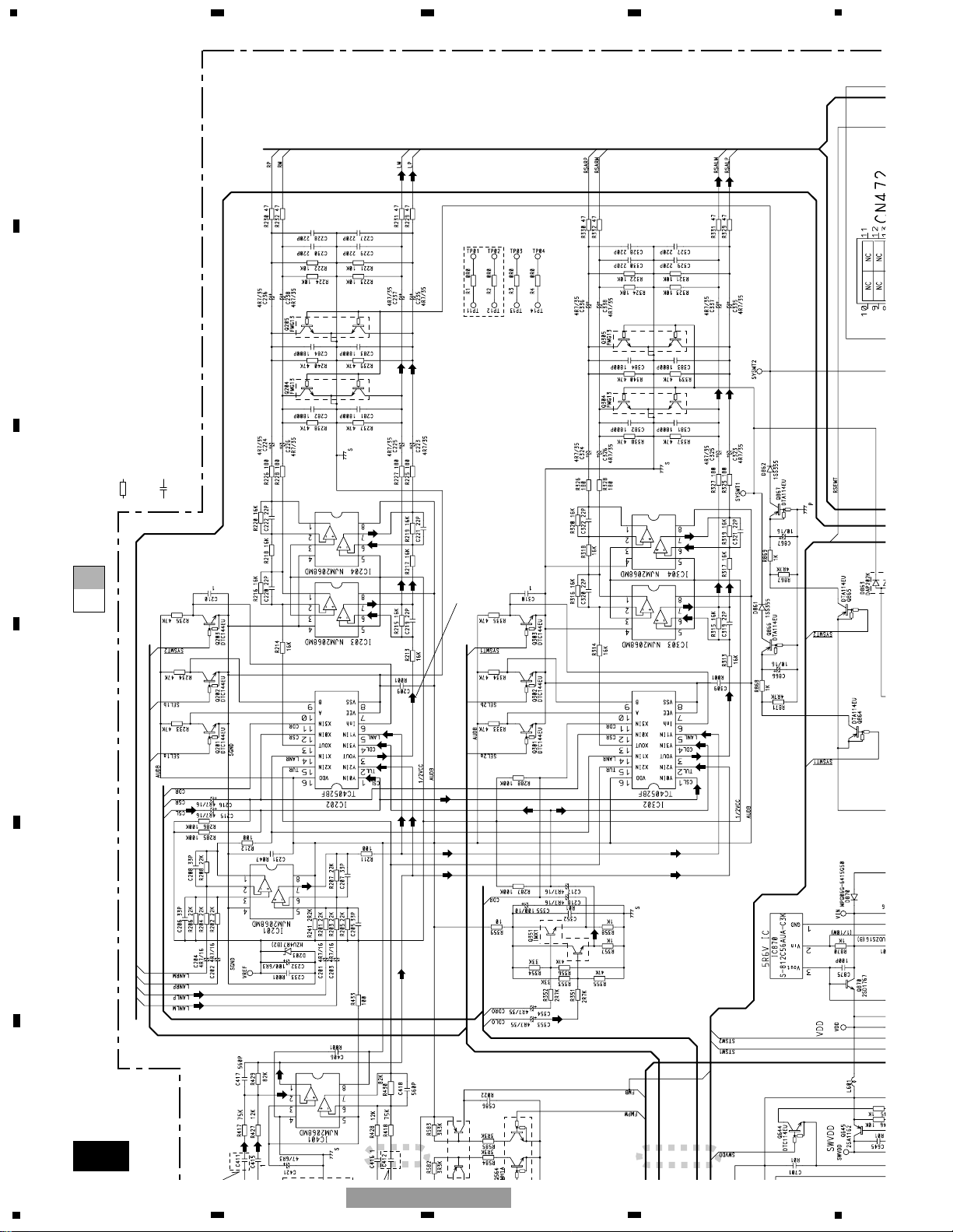
3.3 OVERALL CONNECTION DIAGRAM(GUIDE PAGE)
Page 23
flashLAV
www.club-lexus.ru
A-b
A
Decimal points for resistor
and capacitor fixed values
are expressed as :
2.2 2R2
0.022 R022
←
←
The > mark found on some component parts indicates
the importance of the safety factor of the part.
Therefore, when replacing, be sure to use parts of
identical designation.
Symbol indicates a resistor.
No differentiation is made between chip resistors and
discrete resistors.
NOTE :
Symbol indicates a capacitor.
No differentiation is made between chip capacitors and
discrete capacitors.
FX-MG8337ZT/EW
R022
R022
FX-MG8337ZT/EW
>
350µH
FM: -9.6dBs
AM:-11.5dBs
TAPE: -7.5dBs
CD: +2.3dBs
FM: -3.9dBs
AM: -5.8dBs
TAPE: -1.9dBs
CD:+8.0dBs
4
3
1
5
2
6
4
3
1
5
2
6
4
3
1
5
2
6
431
52
6
4
3
1
5
2
4
3
1
5
2
4
3
1
5
2
4
3
1
5
2
4
3
1
5
2
6
4
3
1
5
2
6
4
3
1
5
2
6
TUNER MIXING AMP
BALANCE TO UNBALANCE
UNBALANCE TO BALANCE
UNBALANCE TO BALANCE
AUDIO SELECTOR
FOR RSA
AUDIO SELECTOR
FOR AMP
SYSTEM MUTE
SYSTEM MUTE
ASENSEBSENSEISENSE
23
5
6
7
8
F
E
D
C
B
A
5
6
7
8
FX-MG8237ZT/EW
Page 24
flashLAV
www.club-lexus.ru
A-a
A-b
A-a
A-a
A-b
1
2
FM/AM TUNER UNIT
A
MAIN UNIT
FX-MG8337ZT/EW
R022
R022
FX-MG8237ZT/EW
R1
R1
C411
C412
FM(30%,400Hz):-24.9dBs
AM(30%,400Hz):-11.8dBs
4
3
1
5
2
4
3
1
52
6
4
3
1
5
2
6
4
3
1
5
2
4
3
1
5
2
4
3
1
5
2
6
4
3
1
5
2
4
3
1
2
6
TUNER MUTE
FM DIVERSITY
RDS DECODER
TUNER
ANTENNA
JACK
24
1
234
12
34
F
E
D
C
B
A
FX-MG8237ZT/EW
Page 25
flashLAV
www.club-lexus.ru
A-a
A-b
A-a
A-a
A-b
3
4
5 6
C
CN501
I
CN251
B
CN901
SYSTEM CONTROLLER
CD(1kHz):+3.6dBs
TAPE(1kHz):-7.5dBs
4
3
1
52
6
4
3
1
5
2
6
25
5
6
7
8
F
E
D
C
B
A
5
6
7
8
FX-MG8237ZT/EW
Page 26
flashLAV
www.club-lexus.ru
A-a
A-b
A-b
1
2
Decimal points for resistor
and capacitor fixed values
are expressed as :
2.2 2R2
0.022 R022
←
←
Symbol indicates a resistor.
No differentiation is made between chip resistors and
discrete resistors.
NOTE :
Symbol indicates a capacitor.
No differentiation is made between chip capacitors and
discrete capacitors.
FX-MG8337ZT/EW
FM: -9.6dBs
AM:-11.5dBs
TAPE: -7.5dBs
CD: +2.3dBs
4
1
2
6
4
3
1
5
6
4
3
1
5
2
4
3
1
5
2
4
3
1
5
2
4
3
1
5
2
4
3
152
6
TUNER MIXING AMP
BALANCE TO UNBALANCE
UNBALANCE TO BALANCE
UNBALANCE TO BALANCE
AUDIO SELECTOR
FOR RSA
AUDIO SELECTOR
FOR AMP
SYSTEM MUTE
SYSTEM MUTE
26
1
234
12
34
F
E
D
C
B
A
FX-MG8237ZT/EW
Page 27
flashLAV
www.club-lexus.ru
A-a
A-b
A-b
3
4
5 6
The > mark found on some component parts indicates
the importance of the safety factor of the part.
Therefore, when replacing, be sure to use parts of
identical designation.
>
350µH
FM: -3.9dBs
AM: -5.8dBs
TAPE: -1.9dBs
CD:+8.0dBs
4
3
1
5
2
6
4
3
152
6
ASENSEBSENSEISENSE
27
5
6
7
8
F
E
D
C
B
A
5
6
7
8
FX-MG8237ZT/EW
Page 28
flashLAV
www.club-lexus.ru
28
B L
R917
R919
R921
B
KEYBOARD PCB
L
LEFT PCB
A
CN804
SEEK•TRACK
DOWN
DISCTAPE
AM FM
4321
56
TAPE EJECTTEXT CD EJECTLOAD
TA
AFPTY
AUDIO
CONTROL•
TUNE
1
234
12
34
F
E
D
C
B
A
FX-MG8237ZT/EW
3.4 KEYBOARD UNIT
Page 29
flashLAV
www.club-lexus.ru
29
B K
2SC4116
R998
4R7K
R999
10K
K
RIGHT PCB
KEYBOARD UNIT
Consists of
KEYBOARD PCB
RIGHT PCB
LEFT PCB
1
5
POWER•VOL
SEEK•TRACK
UP
AST
5
6
7
8
F
E
D
C
B
A
5
6
7
8
FX-MG8237ZT/EW
Page 30
flashLAV
www.club-lexus.ru
C-a
C
D E
F
G H
VR1
ELVSENSE
CCW1023
10K
LOAD1
LOAD2
CAMGEAR MOTOR
M1 CXC1144
LOADING MOTOR
ELEVATION MOTOR
M2 CXC1145
CAMEOK
CAMLOAD
L1
LOAD3
S41
CSN1051
CRG MOTOR
M3 CXC1143
CLAMP
HOME
S2
S1
CSN1057
CSN1057
1
5
12
24
13
SPINDLE
MOTOR
MOTOR DRIVER
CD CONTROL
3+3ch
DRIVER
1K(B)
VCC
1
2
3
4
5
6
7
8
9
10
11
12
13
14
15
16
17
18
19
20
21
22
23
24
25
26
27
28
29
30
CN11
CN12
1
2
3
4
5
CN14
CN13
GR
BL
CN31
RE
WH
6
7
8
9
5
4
3
2
1
6
7
8
9
5
4
3
2
1
CN42
CN1
1
2
3
4
5
6
7
8
9
10
11
12
13
14
15
16
17
CN41
1
2
3
4
5
6
7
8
9
10
11
12
13
14
15
16
17
F
PCB UNIT
(SIDE)
G
PCB UNIT
H
PCB UNIT
(M2 UNIT)
D
PCB UNIT
(LED)
E
PCB UNIT(LOAD)
PU UNIT(SERVICE)(PX1)
F
T
C
S
SIGNAL LINE
FOCUS SERVO LINE
TRACKING SERVO LINE
CARRIAGE SERVO LINE
SPINDLE SERVO LINE
SL
1
2
3
4
5
6
7
8
9
10
11
12
13
14
15
16
17
18
19
20
21
22
23
24
25
26
27
28
29
30
1
2
3
4
5
6
7
8
1
2
3
1
2
3
4
5
6
7
8
T
T
T
T
T
T
T
T
T
T
SL
SL
SL
SL
SL
SL
SL
SL
S
C
C
C
C
C
C
C
C
C
C
S
S
S
S
S
S
S
S
C
F
T
F
T
F
T
F
T
T
T
F
F
T
F
F
T
T
F
F
T
SL
F
F
3
2
4
!
7
9
6
0
5
@
)81
: The power supply is shown with the marked box.
30
1
234
12
34
F
E
D
C
B
A
FX-MG8237ZT/EW
3.5 CD MECHANISM MODULE(GUIDE PAGE)
Page 31

flashLAV
www.club-lexus.ru
C-b
C
SHOCK PROOF
MEMORY
CONTROLLER
BUFFER RAM
3.3V-5V CONVERTER
5V-3.3V CONVERTER
MECHANISM CONTROLLER
5V REGULATOR
3.3V REGULATOR
MUTE
A
CN351
C
CONTROL UNIT(G2T)
SL
SL
SL
#
$
%
^
&
(
*
31
5
6
7
8
F
E
D
C
B
A
5
6
7
8
FX-MG8237ZT/EW
Page 32

flashLAV
www.club-lexus.ru
A-a
C-b
C-a
C-a
C-b
F
G H
1
VR1
ELVSENSE
CCW1023
10K
L1
LOAD3
S41
CSN1051
CRG MOTOR
M3 CXC1143
CLAMP
HOME
S2
S1
CSN1057
CSN1057
1
5
12
24
13
SPINDLE
MOTOR
MOTOR DRIVER
CD CONTROL
3+3ch
DRIVER
1K(B)
VCC
123456789
101112131415161718192021222324252627282930
CN11
CN12
CN14
678954321
678954321
CN42
CN1
123456789
10111213141516
17
CN41
123456789
10111213141516
17
F
PCB UNIT(SIDE)
G
PCB UNIT
H
PCB UNIT
(M2 UNIT)
PU UNIT(SERVICE)(PX1)
123456789
101112131415161718192021222324252627282930
123
4
T
T
T
T
T
T
T
T
T
T
SL
SL
SL
SL
SL
SL
SL
SL
S
C
C
C
C
C
C
S
S
S
S
S
C
F
T
F
T
F
T
TFF
T
TFF
T
SL
F
F
!
7
9
6
0
5
@
)
8
1
32
1
234
12
34
F
E
D
C
B
A
FX-MG8237ZT/EW
Page 33

flashLAV
www.club-lexus.ru
A-a
C-b
C-a
C-a
C-b
D E
2
3
LOAD1
LOAD2
CAMGEAR MOTOR
M1 CXC1144
LOADING MOTOR
ELEVATION MOTOR
M2 CXC1145
CAMEOK
CAMLOAD
3+3ch
DRIVER
30
12345
CN14
CN13
GR
BL
CN31
RE
WH
17
D
PCB UNIT
(LED)
E
PCB UNIT(LOAD)
PU UNIT(SERVICE)(PX1)
30
1234567
8
123
1234567
8
F
T
C
S
SIGNAL LINE
FOCUS SERVO LINE
TRACKING SERVO LINE
CARRIAGE SERVO LINE
SPINDLE SERVO LINE
SL
: The power supply is shown with the marked box.
C
C
C
C
S
S
S
F
F
T
TTF
F
3
2
4
33
5
6
7
8
F
E
D
C
B
A
5
6
7
8
FX-MG8237ZT/EW
Page 34

flashLAV
www.club-lexus.ru
C-a
C-b
C-b
1
SHOCK PROOF
MEMORY
CONTROLLER
BUFFER RAM
3.3V-5V CONVERTER
5V-3.3V CONVERTER
3.3V REGULATOR
MUTE
A
CN351
C
CONTROL UNIT(G2T)
SL
SL
SL
SL
%
^
&
(
*
34
1
234
12
34
F
E
D
C
B
A
FX-MG8237ZT/EW
Page 35

flashLAV
www.club-lexus.ru
C-a
C-b
C-b
2
3
MECHANISM CONTROLLER
5V REGULATOR
3.3V REGULATOR
#
$
35
5
6
7
8
F
E
D
C
B
A
5
6
7
8
FX-MG8237ZT/EW
Page 36

flashLAV
www.club-lexus.ru
36
1
234
12
34
F
E
D
C
B
A
FX-MG8237ZT/EW
Note: The encircled numbers denote measuring points in the circuit diagram.
CH1 : 1 FDX
Mode:Test
CH2 : 2 FOP
CH3 : 3 FOM
CH1 : 5 RFO
CH2 : 6 TE
CH3 : 7 TEC
Mode:Test
CH4 : 4 EC
Focus search mode
CH1 : 5 RFO
Mode:Test
CH2 : 6 TE
CH3 : 8 TDX
1 Track Jump
Tracking open
CH1 : 5 RFO
CH2 : 6 TE
CH3 : 8 TDX
4 Track Jump
Mode:Test
CH1 : 5 RFO
CH2 : 6 TE
CH3 : 8 TDX
10 Track Jump
Mode:Test
CH1 : 5 RFO
CH2 : 6 TE
CH3 : 8 TDX
32 Track Jump
Mode:Test
Page 37

flashLAV
www.club-lexus.ru
37
5
6
7
8
F
E
D
C
B
A
5
6
7
8
FX-MG8237ZT/EW
CH1 : 6 TE
Mode:Normal
CH2 : 9 FE
CH3 : 0 RFI
Focus close
CH1 : $ STSMO
Mode:Normal
CH2 : 6 TE
Memory capacity (remaining) at the starting of PLAY
CH1 : 1 FDX
CH2 : ! FOK
CH3 : @ MDX
CH4 : # FG
Setup
CH1 : 9 FE
CH2 : 1 FDX
CH3 : 6 TE
CH4 : 8 TDX
During "Play"
Mode:Normal
Mode:Normal
CH1 : $ RFO
Mode:Normal
CH2 : 6 TE
Memory capacity (remaining) during PLAY
CH1 : % LRCK
Mode:Normal
CH2 : ^ SCKO
CH3 : & DOUT
Digital audio data(x2 speed)
Page 38

flashLAV
www.club-lexus.ru
38
1
234
12
34
F
E
D
C
B
A
FX-MG8237ZT/EW
CH1 : * LOUT
CH2 : ( ROUT
Mode:Normal
CH1 : 6 TE
CH2 : 8 TDX
Mode:Normal
CH3 : ) SD
Audio output(1kHz , 0dB)
CH1 : 1 FDX
Mode:Normal
CH4 : 4 EC
During inside / outside search
CH2 : ! FOK
CH3 : @ MDX
CH4 : # FG
DISC stop
Page 39

flashLAV
www.club-lexus.ru
39
5
6
7
8
F
E
D
C
B
A
5
6
7
8
FX-MG8237ZT/EW
Page 40

flashLAV
www.club-lexus.ru
DECK UNIT
MUTE
HA12216F
11
12
13
14
15
16
17
18
19
20
40
39
38
37
36
35
34
33
32
31
30
292827
26
252423
22
21
1
234
5
678
9
10
R256
180
R287
0R0
C271
1/50
R284 0R0
R283 0R0
R282 0R0
C254 390P
C253 390P
C252 390P
C251 390P
R281 0R0
R255
180
C256
R01
R258
18K
R402
3R3K
R403 910
C272
R1
R288
0R0
R285 0R0
HD1
HEAD ASSY
EXA1594
TEST TAPE
NCT-150
(400Hz, 200nWb/m)
RL
RR
FR
FL
C302
R1
VR302
33K(B)
-8.24dBs(300mV)±1dB
Fwd-R
Fwd-L
Rev-R
Rev-L
NFI(L)
RIN(L)
RIP
FIN(L)
GND
GND
FIN(R)
VREF
RIN(R)
NFI(R)
M-OUT(R)
EQOUT(R)
TAI(R)
BIAS
RAI(R)
PBOUT(R)
DET(L)
MUTE
MSGV(R)
MAOUT
MSI
MSDET
MSGV
F/R
120/70
NR
MOUT(L)
EQOUT(L)
TAI(L)
NC
RAI(L)
PBOUT(L)
NC
DET(L)
MSGV(S)
CN252
CN251
DOLBY B NR
IC251
VR301
33K(B)
C310
R1
C309
R1
R321
0R0
VCC
CCP1280
CCP1280
NC
MSOUT
NC
NC
R260
13K
R262
270K
C401
3900P
R401
15K
R276
100K
C402
R33
C404
R01
C403
R022
R273
0R0
R272
0R0
C40
Q271
2SC4116
R271
18K
C301
R1
R259
13K
C255
R01
R257
18K
R261
270K
A
I
CN353
R292
0R0
R286 0R0
R296
0R0
I
40
1
234
12
34
F
E
D
C
B
A
FX-MG8237ZT/EW
3.6 CASSETTE MECHANISM MODULE
Page 41

flashLAV
www.club-lexus.ru
41
5
6
7
8
F
E
D
C
B
A
5
6
7
8
FX-MG8237ZT/EW
SWITCHES:
SENSOR UNIT
S101:LOAD SWITCH..........EJECT-PLAY
S102:MODE SWITCH............ON-OFF
S103:70µs SWITCH...............ON-OFF
The underlined indicates the switch position.
R275
47K
R351 1K
R352 1K
R353 1K
R354 1K
R373 0R0
R355
270K
C352
3900P
R362 300
C351 R22
C353 R01
C354 R01
R374 0R0
C356 R01
C355 R1
D352 1SS355
M1 MOTOR UNIT
(MAIN MOTOR)
EXA1618
M2
MOTOR UNIT
(SUB MOTOR)
EXA1623
RS3
RS2
RS1
SC2
SC1
TAB
MC
CE
VCC2
NC
VCC
MCS
RRS
FRS
RSB
C
TAB
MS2
NC
NC
MM
SM1
RSB
GND
RS
mtl
MCS
load
CN255
CN253
CN254
MECHANISM
DRIVER
IC351 PA2020A
R375 0R0
R404
270K
C405
R033
R277
220K
R278
100K
Q271
2SC4116
SENSOR UNIT
S101
LOAD
ESG1007x3
S102
MODE
Q101
EGN1004
CN256
S103
70µs
J
L101
L102
JI
Page 42

flashLAV
www.club-lexus.ru
42
Capacitor
Connector
P.C.Board
Chip Part
A
A
MAIN UNIT
SIDE B
SIDE A
NOTE FOR PCB DIAGRAMS
1.The parts mounted on this PCB
include all necessary parts for
several destination.
For further information for
respective destinations, be sure
to check with the schematic dia gram.
2.Viewpoint of PCB diagrams
C
CN501
B
CN901
I
CN251
CAR HA
76859
4
1
234
12
34
F
E
D
C
B
A
FX-MG8237ZT/EW
4. PCB CONNECTION DIAGRAM
4.1 MAIN UNIT
Page 43

flashLAV
www.club-lexus.ru
43
A
SIDE A
FRONT
FM/AM TUNER UNIT
CAR HARNESS CAR HARNESS
CAR HARNESS
ANTENNA
SUB
MAIN
11112213314415516617718819920
10
111012913814715616517418319220
1
76859410311212
1
5
6
7
8
F
E
D
C
B
A
5
6
7
8
FX-MG8237ZT/EW
Page 44

flashLAV
www.club-lexus.ru
44
A
A
MAIN UNIT
1
234
12
34
F
E
D
C
B
A
FX-MG8237ZT/EW
Page 45

flashLAV
www.club-lexus.ru
45
A
SIDE B
5
6
7
8
F
E
D
C
B
A
5
6
7
8
FX-MG8237ZT/EW
Page 46

flashLAV
www.club-lexus.ru
B
B
KEYBOARD PCB
SIDE A
SEEK•TRACK
DOWN
CD EJECT
TAPE EJECT
1 1 2 2 3 3 4 45 56 6
TEXT
LOAD
TA
DISC
DISC
TAPE
TAPE
FM
AM
AM
FM
46
1
234
12
34
F
E
D
C
B
A
FX-MG8237ZT/EW
4.2 KEYBOARD PCB
Page 47

flashLAV
www.club-lexus.ru
B
B
KEYBOARD PCB
SIDE B
A
CN804
K
CN905
L
CN904
47
5
6
7
8
F
E
D
C
B
A
5
6
7
8
FX-MG8237ZT/EW
Page 48

flashLAV
www.club-lexus.ru
48
C
C
CONTROL UNIT (G2T)
SIDE A
IC,Q
A
CN351
F
CN11
REFO
E
F
1
234
12
34
F
E
D
C
B
A
FX-MG8237ZT/EW
4.3 CD MECHANISM MODULE
Page 49

flashLAV
www.club-lexus.ru
49
C
C
CONTROL UNIT (G2T)
SIDE B
IC,Q
5
6
7
8
F
E
D
C
B
A
5
6
7
8
FX-MG8237ZT/EW
Page 50

flashLAV
www.club-lexus.ru
D
D
PCB UNIT (LED)
E
PCB UNIT (LOAD)
E
F
CN14
M
M2
ELEVATION
RE
WH
CAMOK
CAMLOAD
5
6
7
8
LOAD2
LOAD1
F
CN13
50
1
234
12
34
F
E
D
C
B
A
FX-MG8237ZT/EW
Page 51

flashLAV
www.club-lexus.ru
F
F
PCB UNIT (SIDE)
F
PCB UNIT (SIDE)
SIDE A
SIDE B
E
M
LOADING
VR1
ELV SENSE
1
2
3
4
5
D
CN31
C
CN101
G
8
GR
BL
M
M1
CAMGEAR
51
5
6
7
8
F
E
D
C
B
A
5
6
7
8
FX-MG8237ZT/EW
Page 52

flashLAV
www.club-lexus.ru
M
M3
CRG
1
30
F
CN12
1
9
CN42
1
17
CN41
S41
LOAD3
H
CN1
PU UNIT(SERVICE)(PX1)
L1
G
G
PCB UNIT
52
1
234
12
34
F
E
D
C
B
A
FX-MG8237ZT/EW
Page 53

flashLAV
www.club-lexus.ru
H
H
PCB UNIT(M2 UNIT)
M
SPINDLE
S1
HOME
S2
CLAMP
1
9
CN1
G
CN42
C1
R2
R1
IC1
1
5
1012
13 15
20
24
R4
R3
HE3
HE2
HE1
53
5
6
7
8
F
E
D
C
B
A
5
6
7
8
FX-MG8237ZT/EW
Page 54

flashLAV
www.club-lexus.ru
I
I
DECK UNIT
SIDE A
SIDE B
I
DECK UNIT
CN251
2 4 6 8 10 12 14 16 18 20
1 3 5 7 9 11 13 15 17 19
IC,Q
IC251
Q351
Q352
ADJ
VR302
VR301
IC351
CN252
CN254
CN253
CN255
M1
M2
HEAD ASSY
CN256
21
22
1
10
11
20
21
30
31
40
5
15
25
35
R292
Q271
E
R278
R276
R277
R404
C405
C403
C402
C401
C310
C272
R273
R272
R275
R285
R286
R258
C404
R403
R402
R401
C271
IC251
VR302
R283
R282
R281
R284
C253
R253
C252
R252
R287
R296
R321
R288
R255
R261
C255
R257
R259
C301
R271
C309
VR301
C254
R251
C251
R254
C302
R260
C256
R262
R256
R354
R352
R351
R353
E
E
1
Q271
A
CN353
J
54
1
234
12
34
F
E
D
C
B
A
FX-MG8237ZT/EW
4.4 CASSETTE MECHANISM MODULE
Page 55

flashLAV
www.club-lexus.ru
J
1
2
3
4
5
6
S101
LOAD
S102
MODE
S103
70µs
CN256
Q101
REEL SENSE
L101
L102
I
CN253
J
SENSOR UNIT
55
5
6
7
8
F
E
D
C
B
A
5
6
7
8
FX-MG8237ZT/EW
Page 56

flashLAV
www.club-lexus.ru
K
L
LEFT PCB
SIDE A
L
LEFT PCB
SIDE B
K
RIGHT PCB
SIDE A
K
RIGHT PCB
SIDE B
L
B
CN902
B
CN903
PTY
AST
AST
SEEK•TRACK
UP
PTY
AF
AUDIO CONTROL
•TUNE
POWER•VOL
56
1
234
12
34
F
E
D
C
B
A
FX-MG8237ZT/EW
4.5 RIGHT PCB, LEFT PCB
Page 57

flashLAV
www.club-lexus.ru
Unit Number : CWM8388(FX-MG8237ZT/EW)
Unit Number : CWM8556(FX-MG8337ZT/EW)
Unit Name : Main Unit
MISCELLANEOUS
IC 201 IC NJM2068MD
IC 202 IC TC4052BF
IC 203 IC NJM2068MD
IC 204 IC NJM2068MD
IC 252 IC PM4009A
IC 302 IC TC4052BF
IC 303 IC NJM2068MD
IC 304 IC NJM2068MD
IC 401 IC NJM2068MD
IC 501 IC LA1061M
IC 561 IC HA12181FP
IC 601 IC PD5789A
IC 602 IC
S-80835CNUA-B8U
IC 701 IC HA12187FP
IC 870 IC
S-812C56AUA-C3K
Q 201 Transistor DTC144EU
Q 202 Transistor DTC144EU
Q 203 Transistor DTC144EU
Q 204 Transistor FMG13
Q 205 Transistor FMG13
Q 252 Transistor 2SC3052-12
Q 301 Transistor DTC144EU
Q 302 Transistor DTC144EU
Q 303 Transistor DTC144EU
Q 304 Transistor FMG13
Q 305 Transistor FMG13
Q 351 Transistor IMX1
Q 401 Transistor IMX1
Q 402 Transistor FMG13
Q 403 Transistor FMG13
Q 404 Transistor DTA114EU
Q 405 Transistor DTC143TU
Q 406 Transistor IMH3A
Q 451 Transistor 2SB1260
Q 452 Transistor 2SC2712
Q 453 Transistor 2SC2712
Q 497 Transistor DTC114EU
Q 501 Transistor IMX1
Q 502 Transistor 2SC2712
Q 504 Transistor 2SC2712
Q 561 Transistor 2SC2712
Q 563 Transistor IMT2A
Q 564 Transistor IMH1A
Q 644 Transistor DTC114EU
Q 645 Transistor 2SA1162
Q 721 Transistor DTA114EU
Q 722 Transistor 2SC2712
Q 801 Transistor DTC114EU
Q 802 Transistor IMX1
Q 805 Transistor DTC144TUA
Q 806 Transistor DTC144TUA
Q 807 Transistor DTC144TUA
Q 808 Transistor 2SB1184F5
Q 809 Transistor 2SB1185
Q 811 Transistor 2SB1185
Q 812 Transistor 2SB1185
Q 813 Transistor 2SA1162
Q 814 Transistor 2SA1162
Q 815 Transistor IMX1
Q 816 Transistor 2SC4081
Q 818 Transistor 2SB1184F5
Q 819 Transistor 2SA1162
Q 820 Transistor IMX1
Q 822 Transistor 2SD2226K
Q 825 Transistor 2SA1162
Q 860 Transistor 2SA1162
Q 861 Transistor DTC143EU
Q 862 Transistor DTC144TUA
Q 863 Transistor IMD3A
Q 864 Transistor DTA114EU
Q 865 Transistor DTA114EU
Q 866 Transistor DTA114EU
Q 867 Transistor DTA114EU
Q 870 Transistor 2SD1767
Q 882 Transistor 2SA1162
Q 884 Transistor DTC124EU
D 203 Diode HZU4R7(B2)
D 401 Diode 1SS355
D 451 Diode DAN202K
D 452 Diode 1SS355
D 472 Diode MPG06G-6415G50
D 473 Diode MPG06G-6415G50
D 474 Diode 1SS355
D 475 Diode 1SS355
D 497 Diode UDZS20(B)
D 501 Diode 1SV241
D 502 Diode 1SV241
D 503 Diode DAP202K
D 504 Diode 1SS355
D 703 Diode UDZS18(B)
D 704 Diode UDZS18(B)
D 801 Diode 1SS355
D 802 Diode UDZS5R6(B)
D 803 Diode RM4LFJ10
D 804 Diode 1SS355
D 805 Diode UDZS20(B)
D 808 Diode HZU8R2(B2)
D 809 Diode HZU7R5(B3)
D 810 Diode HZU8R2(B2)
D 811 Diode 1SS355
D 812 Diode HZU7R5(B3)
D 813 Diode 1SS355
D 814 Diode HZU8R2(B3)
D 860 Diode HZU8R2(B3)
D 861 Diode 1SS355
57
5
6
7
8
F
E
D
C
B
A
5
6
7
8
FX-MG8237ZT/EW
5. ELECTRICAL PARTS LIST
NOTES:
- Parts whose parts numbers are omitted are subject to being not supplied.
- The part numbers shown below indicate chip components.
Chip Resistor
RS1/_S___J,RS1/__S___J
Chip Capacitor (except for CQS.....)
CKS....., CCS....., CSZS.....
=====Circuit Symbol and No.===Part Name Part No.
--- ------ ------------------------------------------ -------------------------
=====Circuit Symbol and No.===Part Name Part No.
--- ------ ------------------------------------------ -------------------------
A
Page 58

flashLAV
www.club-lexus.ru
D 862 Diode 1SS355
D 863 Diode DAP202K
D 864 Diode 1SS355
D 870 Diode MPG06G-6415G50
D 871 Diode UDZS16(B)
D 882 Diode 1SS355
L 251 Inductor LCTA101J2520
L 252 Inductor LCTC100K3216
L 351 Inductor LCTC2R2K1608
L 352 Inductor LCTC2R2K1608
L 353 Inductor LCTC2R2K1608
L 354 Inductor LCTC2R2K1608
L 355 Inductor CTF1578
L 356 Inductor LCTC2R2K1608
L 357 Inductor CTF1306
L 358 Inductor CTF1306
L 359 Inductor CTF1306
L 360 Inductor CTF1306
L 361 Inductor CTF1306
L 363 Inductor LFEA4R7J
L 505 Ferri-Inductor LAU4R7K
L 506 Coil CTB1102
L 507 Inductor LCTC6R8K3216
L 508 Inductor LCTC6R8K3216
L 509 Inductor LCTC6R8K3216
L 510 Inductor LCTA561J4532
L 511 Inductor LCTA4R7J2520
L 512 Inductor LCTA1R0J2520
L 513 Inductor LCTA1R0J2520
L 514 Inductor LCTA1R0J2520
L 561 Inductor LCTA4R7J2520
L 601 Inductor LCTA100J3225
L 801 Coil 350µH CTH1276
CG 501 Surge Protector DSP-201M-A21F
CG 502 Surge Protector DSP-201M-A21F
X 251 Crystal Resonator 3.648MHz CSS1447
X 601 Radiator 10.0MHz CSS1577
VR 561 Semi-fixed 10kΩ(B) CCP1396
FU 471 Fuse 5A CEK1216
FM/AM Tuner Unit CWE1633
EF 352 EMI Filter CCG1163
RESISTORS
R 1 (FX-MG8337ZT/EW) RS1/16S0R0J
R 2 (FX-MG8337ZT/EW) RS1/16S0R0J
R 3 RS1/16S0R0J
R 4 RS1/16S0R0J
R 201 RS1/16S223J
R 202 RS1/16S223J
R 203 RS1/16S223J
R 204 RS1/16S223J
R 205 RS1/16S223J
R 206 RS1/16S223J
R 207 RS1/16S223J
R 208 RS1/16S223J
R 211 RS1/16S101J
R 212 RS1/16S101J
R 213 RS1/16S163J
R 214 RS1/16S163J
R 215 RS1/16S163J
R 216 RS1/16S163J
R 217 RS1/16S163J
R 218 RS1/16S163J
R 219 RS1/16S163J
R 220 RS1/16S163J
R 221 RS1/16S103J
R 222 RS1/16S103J
R 223 RS1/16S103J
R 224 RS1/16S103J
R 225 RS1/16S181J
R 226 RS1/16S181J
R 227 RS1/16S181J
R 228 RS1/16S181J
R 229 RS1/10S470J
R 230 RS1/10S470J
R 231 RS1/10S470J
R 232 RS1/10S470J
R 233 RS1/16S473J
R 234 RS1/16S473J
R 235 RS1/16S473J
R 237 RS1/16S473J
R 238 RS1/16S473J
R 239 RS1/16S473J
R 240 RS1/16S473J
R 241 RS1/16S222J
R 243 RS1/16S103J
R 244 RS1/16S103J
R 245 RS1/16S103J
R 246 RS1/16S103J
R 247 RS1/16S223J
R 248 RS1/16S223J
R 249 RS1/16S223J
R 250 RS1/16S223J
R 251 RS1/16S153J
R 252 RS1/16S474J
R 253 RS1/16S681J
R 254 RS1/16S0R0J
R 257 RS1/16S102J
R 261 RS1/16S225J
R 267 RS1/16S222J
R 285 RS1/16S104J
R 286 RS1/16S104J
R 287 RS1/16S104J
R 288 RS1/16S104J
R 313 RS1/16S163J
R 314 RS1/16S163J
R 315 RS1/16S163J
R 316 RS1/16S163J
R 317 RS1/16S163J
R 318 RS1/16S163J
R 319 RS1/16S163J
R 320 RS1/16S163J
R 321 RS1/16S103J
R 322 RS1/16S103J
R 323 RS1/16S103J
R 324 RS1/16S103J
R 325 RS1/16S181J
R 326 RS1/16S181J
R 327 RS1/16S181J
R 328 RS1/16S181J
R 329 RS1/10S470J
R 330 RS1/10S470J
R 331 RS1/10S470J
R 332 RS1/10S470J
R 333 RS1/16S473J
R 334 RS1/16S473J
R 335 RS1/16S473J
R 337 RS1/16S473J
R 338 RS1/16S473J
R 339 RS1/16S473J
R 340 RS1/16S473J
R 351 RS1/16S272J
R 352 RS1/16S272J
R 353 RS1/16S333J
R 354 RS1/16S333J
R 355 RS1/16S473J
R 356 RS1/16S473J
R 357 RS1/16S102J
58
1
234
12
34
F
E
D
C
B
A
FX-MG8237ZT/EW
=====Circuit Symbol and No.===Part Name Part No.
--- ------ ------------------------------------------ -------------------------
=====Circuit Symbol and No.===Part Name Part No.
--- ------ ------------------------------------------ -------------------------
Page 59

flashLAV
www.club-lexus.ru
R 358 RS1/16S102J
R 359 RS1/16S100J
R 369 RS1/16S100J
R 401 RS1/16S432J
R 402 RS1/16S432J
R 405 RS1/16S224J
R 407 RS1/16S102J
R 408 RS1/16S102J
R 409 RS1/16S222J
R 410 RS1/16S222J
R 411 RS1/16S224J
R 412 RS1/16S224J
R 413 RS1/16S102J
R 414 RS1/16S102J
R 417 RS1/16S753J
R 418 RS1/16S753J
R 427 RS1/16S123J
R 428 RS1/16S123J
R 429 RS1/16S823J
R 430 RS1/16S823J
R 431 RS1/16S473J
R 432 RS1/16S473J
R 433 RS1/16S101J
R 451 RS1/16S102J
R 452 RS1/16S223J
R 453 RS1/16S823J
R 454 RS1/16S181J
R 455 RS1/16S181J
R 456 RS1/16S181J
R 457 RS1/16S181J
R 458 RS1/16S181J
R 459 RS1/16S223J
R 460 RS1/16S223J
R 474 RS1/8S103J
R 497 RS1/8S221J
R 501 RS1/16S225J
R 502 RS1/16S225J
R 503 RS1/16S225J
R 504 RS1/16S225J
R 505 RS1/16S471J
R 506 RS1/16S104J
R 507 RS1/16S103J
R 508 RS1/16S103J
R 509 RS1/16S334J
R 510 RS1/16S101J
R 511 RS1/16S101J
R 512 RS1/16S104J
R 513 RS1/16S104J
R 514 RS1/16S103J
R 515 RS1/16S182J
R 516 RS1/16S683J
R 517 RS1/16S224J
R 518 RS1/16S473J
R 519 RS1/16S473J
R 520 RS1/16S102J
R 522 RS1/16S222J
R 525 RS1/16S473J
R 526 RS1/16S681J
R 527 RS1/16S681J
R 528 RS1/16S681J
R 529 RS1/16S103J
R 530 RS1/16S681J
R 531 RS1/16S473J
R 532 RS1/16S473J
R 533 RS1/16S472J
R 534 RS1/16S393J
R 535 RS1/16S473J
R 536 RS1/16S103J
R 537 RS1/16S473J
R 538 RS1/16S681J
R 539 RS1/16S681J
R 541 RS1/16S681J
R 542 RS1/16S681J
R 543 RS1/16S681J
R 544 RS1/16S681J
R 545 RS1/16S473J
R 546 RS1/16S103J
R 547 RS1/16S103J
R 548 RS1/16S221J
R 551 RS1/16S0R0J
R 552 RS1/16S0R0J
R 561 RS1/16S104J
R 562 RS1/16S123J
R 563 RS1/16S105J
R 564 RS1/16S562J
R 567 RS1/16S822J
R 568 RS1/16S222J
R 569 RS1/16S184J
R 570 RS1/16S223J
R 571 RS1/16S473J
R 582 RS1/16S332J
R 583 RS1/16S332J
R 584 RS1/16S332J
R 585 RS1/16S332J
R 601 RS1/16S102J
R 602 RS1/16S473J
R 603 RS1/16S102J
R 604 RS1/16S681J
R 605 RS1/16S102J
R 606 RS1/16S0R0J
R 607 RS1/16S104J
R 608 RS1/16S102J
R 609 RS1/16S681J
R 610 RS1/16S0R0J
R 611 RS1/16S0R0J
R 612 RS1/16S102J
R 613 RS1/16S0R0J
R 614 RS1/16S102J
R 615 RS1/16S102J
R 616 RS1/16S102J
R 617 RS1/16S102J
R 618 RS1/16S102J
R 619 RS1/16S0R0J
R 620 RS1/16S0R0J
R 621 RS1/16S681J
R 622 RS1/16S0R0J
R 623 RS1/16S473J
R 624 RS1/16S473J
R 625 RS1/16S473J
R 626 RS1/16S473J
R 627 RS1/16S473J
R 628 RS1/16S0R0J
R 629 RS1/16S472J
R 630 RS1/16S0R0J
R 631 RS1/16S0R0J
R 632 RS1/16S102J
R 633 RS1/16S102J
R 634 RS1/16S102J
R 635 RS1/16S471J
R 637 RS1/16S102J
R 638 RS1/16S102J
R 640 RS1/16S473J
R 641 RS1/16S473J
R 642 RS1/16S104J
R 643 RS1/16S104J
R 644 RS1/16S473J
R 645 RS1/16S102J
R 646 RS1/16S103J
R 647 RS1/16S102J
R 648 RS1/16S102J
59
5
6
7
8
F
E
D
C
B
A
5
6
7
8
FX-MG8237ZT/EW
=====Circuit Symbol and No.===Part Name Part No.
--- ------ ------------------------------------------ -------------------------
=====Circuit Symbol and No.===Part Name Part No.
--- ------ ------------------------------------------ -------------------------
Page 60

flashLAV
www.club-lexus.ru
R 649 RS1/16S222J
R 651 RS1/16S0R0J
R 654 RS1/16S102J
R 655 RS1/16S102J
R 656 RS1/16S102J
R 657 RS1/16S102J
R 658 RS1/16S223J
R 659 RS1/16S102J
R 660 RS1/16S102J
R 661 RS1/16S102J
R 662 RS1/16S102J
R 663 RS1/16S102J
R 664 RS1/16S102J
R 665 RS1/16S102J
R 666 RS1/16S681J
R 667 RS1/16S473J
R 668 RS1/16S473J
R 669 RS1/16S473J
R 670 RS1/16S473J
R 671 RS1/16S473J
R 672 RS1/16S473J
R 673 RS1/16S473J
R 674 RS1/16S473J
R 675 RS1/16S473J
R 676 RS1/16S102J
R 677 RS1/16S102J
R 678 RS1/16S102J
R 679 RS1/16S102J
R 680 RS1/16S102J
R 681 RS1/16S102J
R 683 RS1/16S102J
R 685 RS1/16S102J
R 687 RS1/16S473J
R 689 RS1/16S473J
R 693 RS1/16S0R0J
R 698 RS1/16S102J
R 699 RS1/16S473J
R 701 RS1/16S473J
R 703 RS1/4S101J
R 704 RS1/4S101J
R 705 RS1PMF680J
R 711 RS1/16S473J
R 721 RS1/16S102J
R 722 RS1/16S473J
R 723 RS1/16S103J
R 801 RS1/8S222J
R 802 RS1/8S472J
R 803 RS1/8S472J
R 804 RS1/8S472J
R 805 RS1/8S472J
R 806 RS1/8S472J
R 807 RS1/8S221J
R 810 RS1/16S104J
R 811 RS1/16S104J
R 812 RS1/16S104J
R 819 RS1/16S102J
R 820 RS1/16S123J
R 821 RS1/16S103J
R 822 RS1/16S103J
R 823 RS1/16S223J
R 824 RS1/16S102J
R 825 RS1/16S331J
R 826 RS1/16S103J
R 827 RS1/16S471J
R 828 RS1/16S221J
R 829 RS1/16S223J
R 830 RS1/10S221J
R 831 RS1/16S331J
R 832 RS1/16S471J
R 833 RS1/16S221J
R 840 RS1/4S1R5J
R 841 RS1/4S1R5J
R 842 RS1/4S1R5J
R 843 RS1/4S1R5J
R 844 RS1/16S471J
R 845 RS1/16S471J
R 846 RS1/16S105J
R 847 RS1/10S361J
R 848 RS1/16S3301D
R 849 RS1/16S4301D
R 850 RS1/4S2R2J
R 851 RS1/16S471J
R 852 RS1/16S105J
R 853 RS1/16S102J
R 854 RS1/16S2701D
R 855 RS1/16S4301D
R 856 RS1/16S103J
R 857 RS1/16S103J
R 858 RS1/4S1R5J
R 859 RS1/4S1R5J
R 860 RS1/16S223J
R 861 RS1/16S103J
R 862 RS1/16S104J
R 863 RS1/16S223J
R 865 RS1/16S103J
R 866 RS1/16S103J
R 867 RS1/16S472J
R 868 RS1/16S102J
R 869 RS1/16S102J
R 870 RS1/10S102J
R 871 RS1/16S472J
R 882 RD1/4PU121J
R 884 RS1/16S223J
R 886 RS1/16S472J
R 888 RS1/16S473J
CAPACITORS
C 201 CEALNP4R7M16
C 202 CEALNP4R7M16
C 203 CEALNP4R7M16
C 204 CEALNP4R7M16
C 205 CCSRCH330J50
C 206 CCSRCH330J50
C 207 CCSRCH330J50
C 208 CCSRCH330J50
C 209 CKSRYB102K50
C 210 CKSRYB105K10
C 215 CEALNP4R7M16
C 216 CEALNP4R7M16
C 217 CEALNP4R7M16
C 218 CEALNP4R7M16
C 219 CCSRCH220J50
C 220 CCSRCH220J50
C 221 CCSRCH220J50
C 222 CCSRCH220J50
C 223 4.7µF/35V CCH1016
C 224 4.7µF/35V CCH1016
C 225 4.7µF/35V CCH1016
C 226 4.7µF/35V CCH1016
C 227 CCSRCH221J50
C 228 CCSRCH221J50
C 229 CCSRCH221J50
C 230 CCSRCH221J50
C 231 CKSRYB473K50
C 232 CEAL101M6R3
C 233 CKSRYB102K50
C 235 4.7µF/35V CCH1016
C 236 4.7µF/35V CCH1016
C 237 4.7µF/35V CCH1016
C 238 4.7µF/35V CCH1016
C 243 CKSQYB102K50
C 244 CKSQYB102K50
60
1
234
12
34
F
E
D
C
B
A
FX-MG8237ZT/EW
=====Circuit Symbol and No.===Part Name Part No.
--- ------ ------------------------------------------ -------------------------
=====Circuit Symbol and No.===Part Name Part No.
--- ------ ------------------------------------------ -------------------------
Page 61

flashLAV
www.club-lexus.ru
C 245 CKSQYB102K50
C 246 CKSQYB102K50
C 251 CKSRYB104K16
C 252 CKSRYB104K16
C 253 CEAL220M6R3
C 254 CKSRYB104K16
C 256 CCSRCH270J50
C 257 CCSRCH270J50
C 259 CKSRYB104K16
C 260 CCSRCH471J50
C 261 CCSRCH471J50
C 262 CEAL4R7M35
C 263 CKSRYB473K50
C 264 CKSRYB103K50
C 281 CKSRYB182K50
C 282 CKSRYB182K50
C 283 CKSRYB182K50
C 284 CKSRYB182K50
C 309 CKSRYB102K50
C 310 CKSRYB105K10
C 319 CCSRCH220J50
C 320 CCSRCH220J50
C 321 CCSRCH220J50
C 322 CCSRCH220J50
C 323 4.7µF/35V CCH1016
C 324 4.7µF/35V CCH1016
C 325 4.7µF/35V CCH1016
C 326 4.7µF/35V CCH1016
C 327 CCSRCH221J50
C 328 CCSRCH221J50
C 329 CCSRCH221J50
C 330 CCSRCH221J50
C 335 4.7µF/35V CCH1016
C 336 4.7µF/35V CCH1016
C 337 4.7µF/35V CCH1016
C 338 4.7µF/35V CCH1016
C 351 CEAL4R7M35
C 352 CKSRYB103K50
C 353 4.7µF/35V CCH1016
C 354 4.7µF/35V CCH1016
C 355 CEAL101M10
C 356 CEAL100M16
C 357 CEAL220M10
C 381 CKSRYB182K50
C 382 CKSRYB182K50
C 383 CKSRYB182K50
C 384 CKSRYB182K50
C 401 CKSRYB123K50
C 402 CKSRYB123K50
C 403 4.7µF/35V CCH1016
C 404 4.7µF/35V CCH1016
C 405 CKSRYB153K50
C 406 CKSRYB102K50
C 411 (FX-MG8237ZT/EW) CKSRYB104K16
C 411 (FX-MG8337ZT/EW) CKSRYB223K50
C 412 (FX-MG8237ZT/EW) CKSRYB104K16
C 412 (FX-MG8337ZT/EW) CKSRYB223K50
C 415 CKSRYB105K10
C 416 CKSRYB105K10
C 417 CKSRYB561K50
C 418 CKSRYB561K50
C 421 CEAL470M6R3
C 480 CKSQYB102K50
C 492 CKSRYB473K50
C 493 CCSQCH221J50
C 494 CCSQCH221J50
C 497 CCSRCH221J50
C 503 CKSQYB103K50
C 504 CKSRYB222K50
C 505 CKSRYB222K50
C 506 CKSRYB222K50
C 507 CKSRYB222K50
C 508 CKSRYB103K50
C 509 CKSRYB103K50
C 510 CEAL100M16
C 511 CKSRYB472K50
C 512 CEAL100M16
C 513 CKSRYB473K50
C 514 CEAL2R2M50
C 515 CKSRYB102K50
C 516 CKSRYB103K50
C 517 CKSRYB103K50
C 518 CKSRYB392K50
C 519 CKSRYB103K50
C 520 CKSRYB103K50
C 521 CEAT101M10
C 522 CKSRYB103K50
C 523 CEAL100M16
C 524 CKSRYB472K50
C 525 CKSRYB182K50
C 528 CKSQYB103K50
C 530 CCSRCH100D50
C 561 CEAL3R3M50
C 562 CKSRYB333K16
C 563 CEALNP1R0M50
C 564 CQMA683J50
C 565 CQMA333J50
C 566 CQMA333J50
C 567 CQMA333J50
C 568 CKSRYB105K10
C 569 CKSRYB333K16
C 570 CKSRYB103K50
C 571 CKSRYB682K50
C 572 CEAL101M10
C 573 CKSRYB392K50
C 574 CKSRYB334K10
C 575 CKSRYB102K50
C 585 CKSRYB223K50
C 586 CKSRYB223K50
C 601 CKSRYB102K50
C 602 CKSRYB103K50
C 603 CKSRYB103K50
C 604 CKSRYB104K16
C 605 CEAL220M6R3
C 645 CKSRYB103K50
C 648 CKSRYB102K50
C 671 CCSRCH101J50
C 672 CCSRCH101J50
C 673 CCSRCH101J50
C 674 CCSRCH101J50
C 675 CCSRCH101J50
C 701 CKSRYB103K50
C 703 CCSRCH221J50
C 704 CCSRCH221J50
C 801 CKSRYB102K50
C 802 CEAL1R0M50
C 803 CKSRYB102K50
C 804 2200µF/16V CCH1186
C 805 CKSQYB473K50
C 806 CKSRYB102K50
C 807 CEAL1R0M50
C 808 CKSRYB102K50
C 814 CEAL1R0M50
C 815 CEAL1R0M50
C 816 CKSRYB103K50
C 817 100µF/10V CCH1402
C 818 CKSRYB103K50
C 819 100µF/10V CCH1402
C 820 CKSRYB103K50
C 824 CKSRYB472K50
61
5
6
7
8
F
E
D
C
B
A
5
6
7
8
FX-MG8237ZT/EW
=====Circuit Symbol and No.===Part Name Part No.
--- ------ ------------------------------------------ -------------------------
=====Circuit Symbol and No.===Part Name Part No.
--- ------ ------------------------------------------ -------------------------
Page 62

flashLAV
www.club-lexus.ru
C 825 100µF/10V CCH1402
C 826 CKSRYB472K50
C 828 CKSRYB102K50
C 829 CKSRYB103K50
C 830 CKSRYB103K50
C 831 CKSRYB103K50
C 861 CEAL101M6R3
C 866 CEAL100M16
C 867 CEAL100M16
C 870 CKSRYB103K50
C 871 CKSRYB103K50
C 872 2200µF/16V CCH1186
C 873 CKSRYB105K10
C 875 CCSRCH101J50
C 883 CKSRYB103K50
Keyboard Unit
Consists of
Keyboard PCB
Right PCB
Left PCB
Unit Number : CWS1363
Unit Name : Keyboard Unit
MISCELLANEOUS
IC 901 IC LC75804W
Q 901 Transistor 2SB1132
Q 902 Transistor 2SC4116
Q 903 Transistor 2SB1132
Q 905 Transistor 2SA1162
Q 906 Transistor DTC143EK
Q 907 Transistor 2SA1162
Q 908 Transistor DTC143EK
D 901 Diode 1SS355
D 902 Diode 1SS355
D 903 Diode 1SS355
D 904 Diode 1SS355
D 905 Diode 1SS355
D 906 Chip LED NSCW310-0371
D 907 Chip LED NSCW310-0371
D 911 Chip LED NSCW310-0371
D 912 Chip LED NSCW310-0371
D 916 LED SML-310FC
D 917 LED SML-310FC
D 918 LED SML-310DT
D 919 LED SML-310DT
D 920 Diode HZU4R7(B3)
IL 901 Lamp 8V 60mA CEL1732
IL 902 Lamp 8V 60mA CEL1731
IL 903 Lamp 8V 60mA CEL1731
IL 904 Lamp 8V 60mA CEL1731
IL 905 Lamp 8V 60mA CEL1731
IL 906 Lamp 8V 60mA CEL1731
IL 907 Lamp 8V 60mA CEL1731
IL 908 Lamp 8V 60mA CEL1732
IL 911 Lamp 8V 60mA CEL1730
IL 912 Lamp 8V 60mA CEL1730
IL 913 Lamp 8V 60mA CEL1732
IL 914 Lamp 8V 60mA CEL1730
IL 915 Lamp 8V 60mA CEL1730
IL 916 Lamp 8V 60mA CEL1730
IL 917 Lamp 8V 60mA CEL1730
IL 918 Lamp 8V 60mA CEL1732
IL 919 Lamp 8V 60mA CEL1734
IL 920 Lamp 8V 60mA CEL1746
IL 921 Lamp 8V 60mA CEL1746
IL 922 Lamp 8V 60mA CEL1734
IL 923 Lamp 8V 60mA CEL1746
IL 924 Lamp 8V 60mA CEL1746
VR 901 Encoder(AUDIO CONTROL•TUNE) CSD1087
VR 902 Encoder(POWER•VOL) CSD1088
LCD 901 LCD CAW1722
RESISTORS
R 901 RAB4CQ102J
R 902 RS1/16S102J
R 903 RAB4CQ102J
R 905 RS1/16S222J
R 906 RS1/16S222J
R 907 RS1/16S222J
R 908 RS1/16S393J
R 909 RS1/16S681J
R 910 RAB4CQ102J
R 911 RS1/16S471J
R 912 RS1/16S103J
R 914 RS1/16S223J
R 915 RS1/16S223J
R 916 RS1/16S223J
R 917 RAB4CQ0R0J
R 919 RAB4CQ0R0J
R 921 RAB4CQ0R0J
R 923 RS1/8S331J
R 924 RS1/8S331J
R 926 RS1/8S331J
R 927 RS1/8S331J
R 928 RS1/16S103J
R 929 RS1/8S151J
R 931 RS1/8S200J
R 932 RS1/8S200J
R 933 RS1/8S200J
R 934 RS1/8S200J
R 935 RS1/8S200J
R 936 RS1/8S200J
R 942 RS1/16S103J
R 943 RS1/8S151J
R 944 RS1/10S100J
R 945 RS1/10S100J
R 946 RS1/10S180J
R 947 RS1/10S100J
R 948 RS1/10S100J
R 949 RS1/10S100J
R 950 RS1/10S100J
R 951 RS1/10S180J
R 953 RS1/10S151J
R 954 RS1/10S151J
R 955 RS1/10S151J
R 956 RS1/10S151J
R 957 RS1/16S332J
R 958 RS1/16S103J
R 959 RS1/10S151J
R 960 RS1/10S151J
R 961 RS1/10S151J
R 962 RS1/10S151J
R 963 RS1/16S332J
R 964 RS1/16S103J
R 965 RS1/10S100J
R 967 RS1/10S100J
R 968 RS1/10S100J
R 970 RS1/10S120J
R 971 RS1/8S151J
R 972 RS1/8S151J
R 973 RS1/10S100J
R 975 RS1/10S120J
R 976 RS1/10S100J
R 978 RS1/10S100J
R 982 RS1/8S180J
R 983 RS1/8S150J
R 984 RS1/8S180J
R 985 RS1/8S150J
R 988 RS1/8S180J
R 989 RS1/8S150J
R 994 RS1/8S150J
R 995 RS1/8S180J
R 998 RS1/16S472J
62
1
234
12
34
F
E
D
C
B
A
FX-MG8237ZT/EW
=====Circuit Symbol and No.===Part Name Part No.
--- ------ ------------------------------------------ -------------------------
=====Circuit Symbol and No.===Part Name Part No.
--- ------ ------------------------------------------ -------------------------
B
K L
Page 63

flashLAV
www.club-lexus.ru
63
5
6
7
8
F
E
D
C
B
A
5
6
7
8
FX-MG8237ZT/EW
R 999 RS1/16S103J
CAPACITORS
C 906 CKSRYB474K10
C 907 CKSRYB104K25
C 908 CKSRYB104K25
C 909 CKSRYB104K25
C 910 CCSRCH102J50
C 911 CCSRCH101J50
C 913 CCSRCH101J50
C 915 CKSRYB103K50
C 918 CKSRYB104K25
C 919 CKSRYB104K25
C 920 CKSRYB104K25
C 921 CKSRYB104K25
C 922 CCSRCH101J50
C 923 CCSRCH101J50
C 924 CCSRCH101J50
C 925 CCSRCH101J50
Unit Number : CWX2649
Unit Name : Control Unit(G2T)
MISCELLANEOUS
IC 201 IC UPD63711GC
IC 301 IC BD7962FM
IC 302 IC
S-818A33AUC-BGN
IC 303 IC BA05SFP
IC 501 IC SM5903BFP
IC 504 IC TC74VHCT08AFT
IC 505 IC TC74VHC541FT
IC 507 IC
MSM51V17400F6TFT
IC 702 IC PD5748E
Q 101 Transistor 2SB1132
Q 601 Transistor DTC114EK
Q 602 Transistor DTA123JK
Q 603 Transistor DTC314TK
Q 604 Transistor DTC314TK
Q 702 Transistor UMD3N
D 101 Diode 1SS355
D 301 Diode S1G-6904G2P
D 303 Diode S1G-6904G2P
D 601 Chip Diode MA151WA
L 201 Inductor CTF1306
L 601 Inductor CTF1295
TH 701 Thermistor CCX1061
X 201 Radiator 16.93MHz CSS1581
X 701 Radiator 10.00MHz CSS1428
RESISTORS
R 101 RS1/8S120J
R 102 RS1/8S100J
R 103 RS1/16S222J
R 104 RS1/16S102J
R 105 RS1/16S0R0J
R 201 RS1/16S104J
R 202 RAB4CQ681J
R 203 RS1/16S0R0J
R 204 RS1/16S0R0J
R 205 RS1/16S103J
R 206 RS1/16S393J
R 207 RS1/16S0R0J
R 209 RS1/16S0R0J
R 210 RS1/16S0R0J
R 211 RS1/16S0R0J
R 212 RS1/16S562J
R 213 RS1/16S153J
R 214 RS1/16S123J
R 216 RS1/16S0R0J
R 217 RS1/16S0R0J
R 220 RS1/16S471J
R 221 RS1/16S681J
R 298 RS1/16S0R0J
R 301 RS1/16S103J
R 302 RS1/16S153J
R 303 RS1/16S103J
R 304 RS1/16S103J
R 305 RS1/16S272J
R 306 RS1/16S272J
R 307 RS1/16S182J
R 308 RS1/16S272J
R 309 RS1/16S682J
R 310 RS1/16S822J
R 311 RS1/16S103J
R 312 RS1/16S681J
R 313 RS1/16S103J
R 314 RS1/16S153J
R 315 RS1/16S153J
R 316 RS1/16S153J
R 317 RS1/16S103J
R 318 RS1/16S103J
R 319 RS1/16S102J
R 320 RS1/16S392J
R 322 RS1/16S103J
R 323 RS1/16S103J
R 324 RS1/16S103J
R 325 RS1/16S103J
R 501 RS1/16S0R0J
R 504 RS1/16S331J
R 508 RS1/16S682J
R 511 RS1/16S0R0J
R 512 RS1/16S333J
R 513 RS1/16S473J
R 516 RS1/16S331J
R 601 RS1/16S102J
R 602 RS1/16S102J
R 603 RS1/16S223J
R 604 RS1/16S223J
R 605 RS1/16S102J
R 606 RS1/16S681J
R 607 RS1/16S681J
R 608 RS1/16S102J
R 609 RAB4CQ681J
R 701 RAB4CQ104J
R 702 RS1/16S222J
R 703 RS1/16S681J
R 704 RAB4CQ222J
R 705 RAB4CQ681J
R 706 RS1/16S473J
R 707 RS1/16S473J
R 708 RS1/16S222J
R 709 RS1/16S222J
R 711 RAB4CQ104J
R 712 RS1/16S473J
R 713 RS1/16S681J
R 714 RS1/16S473J
R 715 RAB4CQ222J
R 716 RS1/16S103J
R 718 RS1/16S473J
R 719 RS1/16S104J
R 720 RS1/16S103J
R 724 RS1/16S104J
R 727 RS1/16S0R0J
R 734 RS1/16S104J
R 736 RS1/16S681J
R 739 RS1/16S473J
R 741 RS1/16S104J
R 742 RS1/16S222J
R 743 RS1/16S681J
R 758 RS1/16S1502D
=====Circuit Symbol and No.===Part Name Part No.
--- ------ ------------------------------------------ -------------------------
=====Circuit Symbol and No.===Part Name Part No.
--- ------ ------------------------------------------ -------------------------
C
Page 64

flashLAV
www.club-lexus.ru
64
1
234
12
34
F
E
D
C
B
A
FX-MG8237ZT/EW
R 759 RS1/16S103J
R 760 RS1/16S433J
R 767 RS1/16S154J
R 775 RAB4CQ681J
CAPACITORS
C 101 CKSRYB103K25
C 102 CKSRYB104K25
C 103 CEVL101M10
C 104 CEVL470M6R3
C 105 CKSRYB224K16
C 106 CKSRYB224K16
C 107 CKSRYB224K16
C 201 CKSRYB104K25
C 202 CEVL220M16
C 203 CKSRYB473K25
C 204 CKSRYB182K50
C 205 CKSRYB104K25
C 206 CKSRYB152K50
C 207 CKSRYB224K16
C 208 CCSRCH180J50
C 209 CCSRCK2R0C50
C 210 CCSRCH181J50
C 211 CCSRCH510J50
C 212 CKSRYB682K50
C 213 CKSRYB104K25
C 214 CKSRYB104K25
C 215 CKSRYB103K25
C 216 CKSRYB104K25
C 217 CKSRYB104K25
C 218 CKSRYB104K25
C 219 CKSRYB104K25
C 220 CKSRYB104K25
C 221 CEVL470M6R3
C 222 CKSRYB104K25
C 223 CKSRYB102K50
C 224 CKSRYB104K25
C 225 CKSRYB103K25
C 226 CCSRCH220J50
C 301 CEVL101M10
C 302 CKSRYB224K16
C 303 CKSRYB224K16
C 304 10µF/10V CCH1349
C 305 CKSRYB224K16
C 306 10µF/10V CCH1349
C 307 CKSRYB224K16
C 309 CKSYB475K16
C 501 CKSRYB102K50
C 502 CKSRYB104K25
C 503 CKSRYB104K25
C 505 CKSRYB104K25
C 506 CKSRYB104K25
C 508 CKSRYB104K25
C 509 CKSRYB104K25
C 601 CEVL220M6R3
C 602 CEVL220M6R3
C 701 CKSRYB104K25
C 702 CKSRYB104K25
C 703 CKSRYB103K25
C 704 CKSRYB103K25
C 705 CKSRYB104K25
C 706 CKSRYB104K25
C 707 CKSRYB103K25
C 708 CKSRYB473K25
Unit Number :
Unit Name : PCB Unit(Load)
Q 21 Photo-transistor CPT231SCTU
Q 22 Photo-transistor CPT231SCTU
L 21 Inductor LCYBR15J1608
L 22 Inductor LCYBR15J1608
S 21 Spring Switch(LOAD1) CSN1051
S 22 Spring Switch(LOAD2) CSN1052
Unit Number : CWX2614
Unit Name : PCB Unit(LED)
D 31 Chip LED CL205IRXTU
D 32 Chip LED CL205IRXTU
S 31 Spring Switch(CAMLOAD) CSN1052
S 32 Spring Switch(CAMEOK) CSN1052
R 31 RS1/16S0R0J
Unit Number : CWX2611
Unit Name : PCB Unit
L 1 Inductor CTF1389
S 41 Spring Switch(LOAD3) CSN1051
Unit Number : CWX2613
Unit Name : PCB Unit(Side)
MISCELLANEOUS
S 11 Spring Switch(CAMCLMP) CSN1052
VR 11 Semi-fixed 1kΩ(B) CCP1338
RESISTORS
R 11 RS1/16S562J
R 12 RS1/16S562J
R 13 RS1/10S391J
R 14 RS1/10S391J
R 15 RS1/16S0R0J
R 16 RS1/16S0R0J
CAPACITORS
C 12 CKSRYB104K25
Unit Number :
Unit Name : PCB Unit(M2 Unit)
MISCELLANEOUS
IC 1 IC BA6849FS
S 1 Switch(HOME) CSN1057
S 2 Switch(CLAMP) CSN1057
RESISTORS
R 1 RS1/16S221J
R 2 RS1/16S221J
R 3 RS1/16S4R7J
R 4 RS1/16S1R0J
CAPACITORS
C 1 CKSRYB104K16
Unit Number : EWM1043
Unit Name : Deck Unit
MISCELLANEOUS
IC 251 IC HA12216F
IC 351 IC PA2020A
Q 271 Transistor 2SC4116
D 352 Diode 1SS355
VR 301 Semi-fixed 33kΩ(B) CCP1280
VR 302 Semi-fixed 33kΩ(B) CCP1280
=====Circuit Symbol and No.===Part Name Part No.
--- ------ ------------------------------------------ -------------------------
=====Circuit Symbol and No.===Part Name Part No.
--- ------ ------------------------------------------ -------------------------
E
D
G
F
H
I
Page 65

flashLAV
www.club-lexus.ru
65
5
6
7
8
F
E
D
C
B
A
5
6
7
8
FX-MG8237ZT/EW
RESISTORS
R 255 RS1/16S181J
R 256 RS1/16S181J
R 257 RS1/16S183J
R 258 RS1/16S183J
R 259 RS1/16S133J
R 260 RS1/16S133J
R 261 RS1/16S274J
R 262 RS1/16S274J
R 271 RS1/16S183J
R 272 RS1/8S0R0J
R 273 RS1/8S0R0J
R 275 RS1/16S473J
R 276 RS1/16S104J
R 277 RS1/16S224J
R 278 RS1/16S104J
R 281 RS1/8S0R0J
R 282 RS1/8S0R0J
R 283 RS1/8S0R0J
R 284 RS1/8S0R0J
R 285 RS1/8S0R0J
R 286 RS1/8S0R0J
R 287 RS1/8S0R0J
R 288 RS1/8S0R0J
R 292 RS1/8S0R0J
R 296 RS1/16S0R0J
R 321 RS1/8S0R0J
R 351 RS1/16S102J
R 352 RS1/16S102J
R 353 RS1/16S102J
R 354 RS1/16S102J
R 355 RS1/16S274J
R 362 RS1/8S301J
R 373 RS1/16S0R0J
R 374 RS1/8S0R0J
R 375 RS1/16S0R0J
R 401 RS1/16S153J
R 402 RS1/16S332J
R 403 RS1/16S911J
R 404 RS1/16S274J
CAPACITORS
C 251 CKSRYB391K50
C 252 CKSRYB391K50
C 253 CKSRYB391K50
C 254 CKSRYB391K50
C 255 CKSRYB103K50
C 256 CKSRYB103K50
C 271 CEH1R0M50
C 272 CKSRYB104K16
C 301 CKSRYB104K16
C 302 CKSRYB104K16
C 309 CKSRYB104K16
C 310 CKSRYB104K16
C 351 CKSQYB224K25
C 352 CKSRYB392K50
C 353 CKSRYB103K50
C 354 CKSRYB103K50
C 355 CKSQYB104K50
C 356 CKSRYB103K50
C 401 CKSRYB392K50
C 402 CKSRYB334K10
C 403 CKSRYB223K25
C 404 CKSRYB103K50
C 405 CKSRYB333K16
Unit Number : EWM1041
Unit Name : Sensor Unit
MISCELLANEOUS
L 101 Inductor CTF1546
L 102 Inductor CTF1546
S 101 Switch(LOAD) ESG1007
S 102 Switch(MODE) ESG1007
S 103 Switch(70µS) ESG1007
Q 101 Photo-reflector EGN1004
Miscellaneous Parts List
M 1 Motor Unit(MAIN) EXA1618
M 2 Motor Unit(SUB) EXA1623
HD 1 Head Assy EXA1594
M 1 Motor Unit(-A)(CAMGEAR) CXC1144
M 2 Motor Unit(-B)(ELEVATION) CXC1145
M 3 Motor Unit(-A)(CRG) CXC1143
VR 1 Variable Resistor 10kΩ CCW1023
PU Unit(Service)(PX1) CXX1569
=====Circuit Symbol and No.===Part Name Part No.
--- ------ ------------------------------------------ -------------------------
=====Circuit Symbol and No.===Part Name Part No.
--- ------ ------------------------------------------ -------------------------
J
Page 66

flashLAV
www.club-lexus.ru
66
1
234
12
34
F
E
D
C
B
A
FX-MG8237ZT/EW
6. ADJUSTMENT
6.1 CONNECTION DIAGRAM
GGD1239
GGD1318
Bullet connector
(To DC Regulated Power Supply)
Bullet connector
SP Line
Bullet connector
(To DC Regulated Power Supply)
Bullet connector
(To DC Regulated Power Supply)
FX-MG8237ZT/EW
FX-MG8337ZT/EW
GM-8337ZT/E
H/U
EMV
12P
20P
6P
10P
14P
8P
10P
18P
32P
18P
10P
6P
10P
14P
12P
20P
20P
24P
8P
20P
20P
20P
24P
GGD1317
AUI+AUI-
FR+FR-
AMP
NAVI ECU
- EMV/NAVI SYSTEM(AMP:P AND M/L)
M/L AMP SYSTEM cannot use GGD1317.
Because, external connector is different from pioneer AMP and
M/L AMP(PIO:24P-20P,M/L:25P-16P).
Moreover, GGD1240 which is a previous jig cannot be used
(Because the signal array is different).
Therefore, when the head unit of the M/L AMP system is
repaired, pioneer AMP system is used.
* P and Pio : Pioneer
* M/L : Mark Levinson
Page 67

flashLAV
www.club-lexus.ru
67
5
6
7
8
F
E
D
C
B
A
5
6
7
8
FX-MG8237ZT/EW
- STANDARD SYSTEM(AMP:P AND M/L)
GM-8337ZT/E
GGD1317
Bullet connector
(To DC Regulated Power Supply)
Bullet connector
SP Line
H/U
20P
12P
20P
24P
20P
20P
20P
24P
AMP
FX-MG8237ZT/EW
FX-MG8337ZT/EW
M/L AMP SYSTEM cannot use GGD1317.
Because, external connector is different from pioneer AMP and
M/L AMP(PIO:24P-20P,M/L:25P-16P).
Moreover, GGD1240 which is a previous jig cannot be used
(Because the signal array is different).
Therefore, when the head unit of the M/L AMP system is
repaired, pioneer AMP system is used.
* P and Pio : Pioneer
* M/L : Mark Levinson
Page 68

flashLAV
www.club-lexus.ru
68
IC601
MAIN UNIT
DC Regulated
Power Supply
BACK UP
ACC
GND
+13.2V
GND
FM/AM TUNER UNIT
DECK UNIT
Extention Cord GGD1121
VR561
VR302
mV
Meter(1)
VR301
L-CH
R-CH
Pin2
Pin3
CN251
DECK UNIT
- Connection Diagram
DOLBY B NR ADJUSTMENT
No. Test Tape Adjustment Point Adjustment Method
(Switch Position)
1 NCT-150 VR301(Lch),VR302(Rch) mV Meter(1) : –8.24dBm(300mV)±1dB
(400Hz,200nwb/m) (DOLBY NR Switch : OFF)
1
234
12
34
F
E
D
C
B
A
FX-MG8237ZT/EW
6.2 AUDIO, TUNER ADJUSTMENT
Page 69

flashLAV
www.club-lexus.ru
69
5
6
7
8
F
E
D
C
B
A
5
6
7
8
FX-MG8237ZT/EW
Connection:
Setting of the pulse generator (setting of
superimposed pulse)
Adjustment:
1. Setting of SSG
Receiving frequency : 999 kHz
Percentage modulation : 30%
Modulation frequency : 400 Hz
Antenna input : 74 dBuV (EMF)
2. Tune a RADIO to the "999kHz" with 1' condition.
3. Mix signal with the above-mentioned pulse and
SSG moduration OFF.
4. Variable resistance adjust noise level to a
minimam.
Adjustment point : VR561
Pulse generator
(equivalent to HP8011A)
SSG
2-signal pad AM dummy
KEX-M8406ZT
Output
Noise meter
Pulse width :50usec
Pulse intervals :5msec
Pulse voltage :4Vp-
p
4Vp-p(EMF)
50us
5ms
AM NOISE CANCELER ADJUSTMENT
FX-MG8237ZT/EW
FX-MG8337ZT/EW
Page 70

flashLAV
www.club-lexus.ru
70
1
234
12
34
F
E
D
C
B
A
FX-MG8237ZT/EW
6.3 TEST MODE
[1] + [6] + [DISC]: 3 times
DIAG IN
P190
[DISC] + [UP]
PBUS Test Mode In
PBUS TEST
[DISC]: for 1.7 seconds
DIAG End
Normal display
[DISC]
CD On
CD *
(*: Disc number)
To the CD Test Mode
Key to be pressed
Operation
Display
[3] + [TA]
External CD-CH
Test Mode In
(*1)
[3] + [AF]
External CD-CH
Error number displayed
CD ERRXX
[4] + [DOWN]
Internal CD-CH
Error number displayed
CD ERRXX
Notes:
*1) Depending on the state of DIAG
*2) Note that the test mode is cancelled in the system microcomputer
by switching the ACC OFF and ON, but that it is not in the CD microcomputer.
Use the reset function for complete cancellation of the test mode.
Rest the Microcomputer to
return to the normal mode.(*2)
Page 71

flashLAV
www.club-lexus.ru
71
5
6
7
8
F
E
D
C
B
A
5
6
7
8
FX-MG8237ZT/EW
1) Precautions on Adjustment
• The unit employs a single voltage (+5V) for the regulator, thus the reference potential of the signal is
REFO (approximately 2.5V) rather than GND.
Inadvertent contact of REFO and GND during adjustment can result not only in disabling normal potential
measurement but also in exposing the pickup to
strong impacts due to malfunctioning of the servo.
Therefore, you are requested to observe the following
precautions.
• Make sure that the negative probe of the measuring
instrument is not connected to REFO or GND. Special
care must be exercised so that the channel 1 negative
probe may not be connected to the oscilloscope and
the channel 2 negative probe to GND. Since the
frame of the measuring instrument is usually at the
same potential as the negative probe, the frame of
the measuring instrument must be changed to floating status.
When REFO is inadvertently connected to GND, you
must immediately turn off the regulator or power
supply.
• The regulator must be turned off before mounting or
dismounting filters or wiring materials.
• You should not start adjustment or measurement
immediately after the regulator is turned on. It is recommended to run the player for approximately one
minute so that it may stabilize.
• When the test mode is turned on, various protective
functions from the software become unavailable.
Thus, you must make sure that undesirable electric or
mechanical shocks are not be given to the system.
• This model employs a photo-transistor for detecting
discs at their loading or ejection. Thus, if its outer
case is removed during repair work and internal parts
are exposed to light of strong intensity, malfunctions
including the following can result:
∗ The eject button becomes inoperable during play.
Pressing the eject button does not eject a disc and
play is continued.
∗ Loading becomes unavailable.
If a malfunction is recognized, appropriate remedial
actions must be taken. Such actions include changing the light source position, changing the unit position and applying a cover to the photo-transistor.
• When you press the EJECT key to eject a disc, you
must not touch any other key until the ejection is
complete.
• If you press the UP or DOWN for the focus search in
the test mode, you must turn the power off immediately. (Otherwise, the lens will be forced to stick to
the top or bottom, potentially resulting in the burning
of the actuator.)
2) Description of the Test Mode
• Turning on the Test Mode
See page 70.
• Ending the Test Mode
Apply the reset (the reset will be applied two minutes
after the power is turned from off).
• Operation of TR JUMPs (except 100TR) continues
after your finger has left the key. CRG, MOVE and
100TR JUMP are forced to the tracking close mode as
soon as the key is released.
• Turning the power on or off resets the JUMP MODE
to the Single TR.
6.4 CD ADJUSTMENT
Page 72

flashLAV
www.club-lexus.ru
72
1
234
12
34
F
E
D
C
B
A
FX-MG8237ZT/EW
- Flow Chart
Power Off
TRK
[TXT]
Power Off
MIN
TRK
[Key]
Contents
Display
Power ON
(T.OFFSET adjustment required)
TRK
00
[TXT]
SEC
MIN
Tracking Close
(AGC, Applicable Servo)
TRK
SEC
[1]+[6]+[DISC]3times
Diag Mode In
[DISC]+[SEEK UP]
Test Mode In
[DISC] 3sec
Diag off
[DISC]
Source CD
SEC
MIN
TRK
[TXT]
SEC
MIN
00 00
[5]
Focus Close/S-curve/
F, F0 Measurement
SEC
MIN
TRK
91 91
91
[1]
SEC
MIN
xx xx
xx
MIN
99
SEC
0x 0x
SEC
[5]
SEC
99 99
*2
TRK
or
TRK
Power ON
(T.OFFSET adjustment not required)
TRK
[SEEK DOWN]
Focus Mode Select
MIN
TRK
0x
[SEEK DOWN]
Tracking Close
(No AGC, Applicable Servo)
MIN
TRK
xx xx
xx
RF AMP Gain Select
TRK
[1]
Tracking Servo
Close
SEC
MIN
00 00
00
SEC
MIN
99 99
99
Rough Servo and RF AGC/
RF AGC Factor Display
[5]
SEC
MIN
TRK
?? ??
??
[2]
*1
SEC
MIN
00 00
00
[TA]
CRG+
TRK
or
TRK
SEC
MIN
00 00
00
SEC
MIN
99 99
99
TRK
or
TRK
[TA]
CRG+
*9
MIN
TRK
8x 8x
8x
or
MIN
TRK
9x 9x
9x
[1]
Mechanism Test Mode
Initial State
MIN
TRK
00 00
72
[AF]
CRG-
SEC
MIN
00 00
00
SEC
MIN
99 99
99
CRG-
SEC
TRK
8x
or
SEC
TRK
9x
SEC
MIN
MIN
[AF]
8x 8x
9x 9x
SEC
SEC
[SEEK DOWN]
New Test Mode
SEC
MIN
TRK
TRK
??
[2]
SEC
MIN
?? ??
Tracking Balance
Adjustment
TRK
8x
[2]
MIN
8x 8x
Auto Adjustment Display
Select
*3
SEC
[TXT]
Power Off
SEC
MIN
TRK
[TXT]
Power Off
SEC
MIN
SEC
MIN
SEC
MIN
00
00
SEC
MIN
99
99
Single TR
9X(8X):91(81)
TRK
→→
TRK
06
S.Curve Check
→→
TRK
00
)
99
→→→F.Offset Display
RF Offset Display T.Bal Display
( F.Cancel value
= (Upper 8 bits of the setting (7F[H] to 80[H] + 128)/4
= 63[D] to 32[D] to 00[D]).
→→ → → →
4 TR
92(82)
*1)
TRK
*2)
TRK
(TRK
*3)
*4) Single TR /4TR / 10TR / 32TR / 100TR
*5)
*6) Only for the CRG Move and 100TR modes
Track No. / Min / Sec
*7)
(F.T. AGC Gain = (Current value/Initial value) x 20)
→→→
F.AGC Gain T.AGC Gain
*8) CRG motor voltage : 2 [ V ]
*9)
The first press displays the RF AGC coefficient. The second one or after performs the rough servo and RF AGC adjustments, and then displays the RF AGC coefficient.
In all TR Jump modes except for 100TR, track jump operation continues even after the key is released.
•
In the CRG Move and 100TR Jump modes, the tracking servo loop closes at the same time when the key is released.
When the power is turned off and on, the jump mode, the RF AMP gain
•
setting, and the auto adjustment values are reset to the Single TR (91),0dB, and the factory setting respectively.
Note: When you pressed the
(otherwise, the lens can stick resulting in actuator damages).
F,T,RF AGC
Display Switching
TRK
-6dB
SEC
MIN
06
SEC
MIN
01
01
10 TR
93(83)
[1]
*7
SEC
MIN
?? ??
??
-12dBTYP
SEC
MIN
TRK
12
12
12
06
LD OffFocus Close
MIN
TRK
02
32 TR
94(84)
02
100 TR
95(85)
01
[5] [SEEK DOWN]
F,T AGC and
RF AGC
SEC
SEC
MIN
TRK
xx xx
xx
02
Rough Servo.
CRG Move
96(86)
RF AGC Gain
CRG/TR Jump Count
*5
Select
SEC
MIN
TRK
xx xx
xx
[Key]
[TXT]
[TA]
[AF]
[1]
[2]
[5]
[SEEK DOWN]
[LOAD]
[EJECT]
[4] (DISC UP)
[3] (DISC DOWN)
CRG+/TR Jump+
TRK
xx
Power ON/OFF
CRG+/TR Jump+
(Toward outer perimeter)
CRG-/TR Jump(Toward inner perimeter)
Tracking close and AGC and Applicable
servo / AGC , AGC display switching
RF gain select / Offset adjustment display/
Tracking balance adjustment / Tracking open
Focus Close, S.Curve /
Rough Servo/ RF AGC / F,T, RF AGC
Focus mode select / Tracking close /
CRG.TR jump select
DISC load
DISC eject
DISC UP
DISC DOWN
[TA] or [AF] key during the Focus Search, you must turn the power off immediately
[TA]
MIN
SEC
xx xx
*4
CRG–/TR Jump–
TRK
TRK
or
TRK
Test Mode
[AF]
MIN
xx xx
xx
[2]
Trackig Open
MIN
8x 8x
8x
MIN
9x 9x
9x
*4
SEC
*6
SEC
SEC
Operation
[2]
Trackig Open
MIN
TRK
8x 8x
8x
or
MIN
TRK
9x 9x
9x
SEC
SEC
New Test Mode
Error occurrence time/
Cause display switching
DISC load
DISC eject
DISC UP
DISC DOWN
Page 73

flashLAV
www.club-lexus.ru
73
• Note :
The grating angle of the PU unit cannot be adjusted after the PU unit is changed. The PU unit in the CD mecha-
nism module is adjusted on the production line to match the CD mechanism module and is thus the best adjusted
PU unit for the CD mechanism module. Changing the PU unit is thus best considered as a last resort. However, if
the PU unit must be changed, the grating should be checked using the procedure below.
• Purpose :
To check that the grating is within an acceptable range when the PU unit is changed.
• Symptoms of Mal-adjustment :
If the grating is off by a large amount symptoms such as being unable to close tracking, being unable to perform
track search operations, or taking a long time for track searching.
• Method :
• Measuring Equipment • Oscilloscope, Two L.P.F.
• Measuring Points • E, F, REFO
• Disc • ABEX TCD-784
• Mode • TEST MODE
• Checking Procedure
1. In test mode, load the disc and switch the 5V regulator on.
2. Using the TA and AF buttons, move the PU unit to the innermost track.
3. Press key 5 to close focus, the display should read "91". Press key 2 to implement the tracking balance adjust
-
ment the display should now read "81". Press key 5 4 times. The display will change, returning to "81" on the
fourth press.
4. As shown in the diagram above, monitor the LPF outputs using the oscilloscope and check that the phase differ
-
ence is within 75° . Refer to the photographs supplied to determine the phase angle.
5. If the phase difference is determined to be greater than 75° try changing the PU unit to see if there is any
improvement. If, after trying this a number of times, the grating angle does not become less than 75° then the
mechanism should be judged to be at fault.
• Note
Because of eccentricity in the disc and a slight misalignment of the clamping center the grating waveform may be
seen to "wobble" ( the phase difference changes as the disc rotates). The angle specified above indicates the aver
-
age angle.
• Hint
Reloading the disc changes the clamp position and may decrease the "wobble".
100kΩ
390pF
100kΩ
390pF
E
REFO
F
Xch Ych
Oscilloscope
L.P.F.
L.P.F.
REFO
CONTROL UNIT(G2T)
REFO
E
F
5
6
7
8
F
E
D
C
B
A
5
6
7
8
FX-MG8237ZT/EW
6.5 CHECKING THE GRATING AFTER CHANGING THE PICKUP UNIT
Page 74

flashLAV
www.club-lexus.ru
74
Grating waveform
Ech → Xch 20mV/div, AC
Fch → Ych 20mV/div, AC
45°
0°
75°
60°
30°
90°
1
234
12
34
F
E
D
C
B
A
FX-MG8237ZT/EW
Page 75

flashLAV
www.club-lexus.ru
75
5
6
7
8
F
E
D
C
B
A
5
6
7
8
FX-MG8237ZT/EW
6.6 TEST MODE(CD)
Manual test
Select the motor you desire to move by using one of the following four keys: [1], [2], [5], and [6].
After selecting the motor, use the [TA] or [AF] key tomove the selected motor. While the key is being pressed, the motor will keep moving.
1. To select the CAM motor,
press the key [1].
For the CAM PLAY direction,
use the key [TA].
For the CAM ELV direction,
use the key [AF].
2. To select the ELV motor,
press the key [2].
For the ELV UP direction,
use the key [TA].
For the ELV DOWN direction,
use the key [AF].
3. To select the LOAD motor,
press the key [5]. (Default)
For loading, use the key [TA].
For ejection, use the key [AF].
4. To select the SPDL claws, press the key [6].
Caution: SPDL claw test should be performed in the servo test mode. The
SPDL claws are controlled by the servo systems and the switches conditions
cannot be checked in the mechanical test mode.
To open the claws, use the key [TA].
To close the claws, use the key [AF].
Durability test
To enter the durability test modes, press the key [SEEK UP].
To exit from the test modes, press one of the keys [1], [2], [5], and [6].
1. LOAD durability test (Load <-> Eject)
At the door open position (disc insertion/eject position), insert a disc and press
the key [SEEK UP].
2. CAM durability test (Play <-> ELVOK)
At any position between CAM4P and CAM5P (display: 06, 04), press the key [SEEK UP].
3. LIFT durability test (Current disc <-> Door Open)
At any position between CAM2P and CAM3P (display: 05, 07), press the key [SEEK UP].
4. ELV durability test (ELV1F <-> 6F)
At the CAM1P position (display: 01), press the key [SEEK UP].
.
[Key]
Operation
Display
[1]
CAM MOTOR
Selection
MIN
TRK
01 **
72
SEC
[1] + [6] + [DSIC]: 3 times
DIAG Mode In
[SEEK UP] + [DISC]
Test Mode In
PBUS TEST
[DISC]: for 3 seconds
DIAG Off
[CD] or [DISC]
Source CD
SEC
MIN
TRK
**** **
[1]
Mech Test In
Initial state
SEC
MIN
TRK
** **
72
[5]
LOAD MOTOR
Selection
SEC
MIN
TRK
00
72
bit2:CamEokSW OFF
bit1:CamloadSW
bit0:CamclampSW
Display
Mech test mote
Display
Mech test mote
Display
Mech test mote
[2]
ELV MOTOR
TRK
72
Display
Mech test mote
Selection
SEC
MIN
02 ****
Track Minute
72 01
CAM1P
(01H)
DISC CLAMP
SELECTION
TRK
72
CAM motor selected
E
L
V
CAM1P
(01H)
ON
OFF
ON
OFF
ON
The states of the CAM switches
Track Minute Second
72 02
ELV motor selected
Track Minute Second
72 00
Track Minute Second
* *
Eudpzt (ELV position x2)
* *
LOAD motor selected
72 03 00
SPDL claws selected
0 fixed
[6]
SEC
MIN
03 **
TRK
Second
* *
L
C
I
L
F
M
T
P
CAM1P
CAM1P
(01H)
[SEEK UP]
SELECTION
RESET
MIN
** **
72
P
L
A
Y
(01H)
bit12:loadpht
bit11:loadsidesw
bit10:loadoksw
Display
[TXT]
CAM1P
(01H)
Mech Test In
MIN
TRK
**
SEC
[SEEK UP]
OFF
ON
OFF
ON
OFF
ON
The states of the loading switches
Track Minute Second
* *
Mech test mode (72)
An error occurs.
Error mode display
SEC
** **
Key
[TXT]
[TA]
[AF]
To the mech test initial state
Moves the motor selected by one of the keys B3H to B6H,
in the FWD direction. The motor keeps moving while the key is pressed.
Moves the motor selected by one of the keys B3H to B6H,
in the REV direction. The motor keeps moving while the key is pressed.
Selects the CAM motor.
[1]
[2]
Selects the ELV motor.
Selects the LOAD motor.
[5]
Selects the DISC CLAMP.
[6]
Selection reset.
Halfemp fill
* * * *
The number of loops (Max. 999)
Operation
Page 76

flashLAV
www.club-lexus.ru
76
Mode
Electrical error
Servo error
1,2
1,2
3,4
1,2
1,2
1,2
1,2
1,2
1,2
1,2
3
4
A0
A1
10
11
12
14
17
19
30
VD power NG
Mech Vref NG
Carriage home NG
Focus search NG
Spindle Lock NG Subcode
Mirror NG
Setup NG
Tracking Balance NG
Search time-out
VD power abnormal
Mech elevation reference voltage abnormal
At the occurrence of error, motor control output (*6)
The CRG cannot move to inner tracks or move from inner tracks.
No focus
No spindle lock. Sub codes cannot be read.
Not applicable to the G2 mech.
AGC protection does not function. Focus is easily unlocked.
Not applicable
Cannot reach the target address.
At the occurrence of error, claw switch value
The rotation rate does not satisfy the spec.
ERROR 4
ERROR 4
ERROR 3
ERROR 1
ERROR 1
ERROR 1
ERROR 1
Digit Code
Name
Descriptions
AVC-LAN
error code
Mode
Waiting for disc pulled out
CAM Err
CAMRST Err
1,2
1,2
1,2
1,2
1,2
1,2
1,2
3
4
1,2
1,2
1,2
1,2
1,2
1,2
1,2
1,2
1,2
1,2
1,2
1,2
1,2
1,2
1,2
1,2
1,2
1,2
1,2
1,2
1,2
1,2
3
4
1,2
1,2
1,2
1,2
20
21
22
23
24
25
26
51
52
5a
5b
5e
61
62
64
66
6a
6b
71
72
7a
7b
7d
7f
81
82
8a
8b
aa
91
92
93
94
MFWDTO
MREVTO
MFWDTO
MREVTO
MFWD2TO
MFWDTO
MREVTO
MLSWNG
MREV2TO
MFWDTO
MREVTO
MFWDTO
MREVTO
MFWDTO
MREVTO
MLSWNG
MREV2TO
MFWDTO
MREVTO
MFWDTO
MREVTO
MOVERCNT
MFWDTO
MREVTO
MOVERCNT
MSPDERR
CAMRST Forced ejection Waiting for disc pulled out
WTLOAD Forced ejection Waiting for disc pulled out
EJCTON Forced ejection Waiting for disc pulled out
SEJPCK Forced ejection Waiting for disc pulled out
HLFLOAD Forced ejection Waiting for disc pulled out
DINSRDY Forced ejection Waiting for disc pulled out
LIFTDN LIFTUP Forced ejection Waiting for disc pulled out
The m2stat value at the original error followed by forced ejection (*3)
The LOAD SW value (3 bits) at the forced ejection end:
CAM motor FWD time-out error during TRAY UP operation
CAM motor REV time-out error during TRAY UP operation
CAM motor FWD time-out error during TRAY DN operation
CAM motor REV time-out error during TRAY DN operation
CAM motor FWD2 time-out error during TRAY DN operation
CAM motor FWD time-out error during CRG OUT operation
CAM motor REV time-out error during CRG OUT operation
LOAD SW ON stuck error during CRG OUT operation
CAM motor REV2 time-out error during CRG OUT operation
CAM motor FWD time-out error during CRG IN operation
CAM motor REV time-out error during CRG IN operation
CAM motor FWD time-out error during ELV IN operation
CAM motor REV time-out error during ELV IN operation
CAM motor FWD time-out error during ELV OUT operation
CAM motor REV time-out error during ELV OUT operation
LOAD SW ON stuck error during ELV OUT operation
CAM motor REV2 time-out error during ELV OUT operation
CAM motor FWD time-out error during EIN_EXP operation
CAM motor REV time-out error during EIN_EXP operation
CAM motor FWD time-out error during CIN_EXP operation
CAM motor REV time-out error during CIN_EXP operation
CAM SW has not been determined during CAM operation (Chatter remains.)
The OK stop position at the last elevation operation (*4)
The CAM SW value (3 bits) before retry (with the first error)
ELV motor FWD time-out error during CAMRST operation
ELV motor REV time-out error during CAMRST operation
Over-count error during CAMRST operation
The claws do not close during CAMRST operation.
ERROR 3
ERROR 3
ERROR 3
ERROR 3
ERROR 3
ERROR 3
ERROR 3
ERROR 3
ERROR 3
ERROR 3
ERROR 3
ERROR 3
ERROR 3
ERROR 3
ERROR 3
ERROR 3
ERROR 3
ERROR 3
ERROR 3
ERROR 3
ERROR 3
ERROR 3
ERROR 3
ERROR 3
ERROR 3
ERROR 3
ERROR 3
ERROR 3
ERROR 3
ERROR 3
ERROR 3
ERROR 3
ERROR 3
Digit Code
Name
Descriptions
AVC-LAN
error code
- Electrical and servo errors
- Mechanical errors
1
234
12
34
F
E
D
C
B
A
FX-MG8237ZT/EW
Page 77

flashLAV
www.club-lexus.ru
77
Mode
1,2
3
4
1,2
1,2
1,2
1,2
3
4
1,2
1,2
1,2
1,2
3
4
1,2
1,2
1,2
1,2
1,2
1,2
1,2
1,2
1,2
1,2
3
4
1,2
1,2
1,2
1,2
1,2
1,2
1,2
1,2
1,2
1,2
1,2
1,2
1,2
1,2
1,2
1,2
3
4
1,2
1,2
1,2
1,2
3
4
96
9a
9b
9c
9d
b1
b2
b3
b6
c1
c2
c3
c6
d1
d2
d3
d4
d6
d7
90
eb
ed
fb
e0
e2
e6
f0
f1
f2
f3
f4
f5
f6
f7
ab
40
41
42
43
MREV2TO
MSPDERR
MSPDERR
MSPDERR
MSPDERR
MFWDTO
MREVTO
MOVERCNT
MREV2TO
MFWDTO
MREVTO
MODERCNT
MREV2TO
MFWDTO
MREVTO
MOVERCNT
MLSWNG
MREV2TO
MLSW2NG
BACKUP_NG
MLSWNG
MLSWNG
MLSWNG
BACKUP_NG
MREVTO
MREV2TO
BACKUP_NG
MFWDTO
MREVTO
MCHTERR
MLSWNG
MFWD2TO
MREV2TO
MLSW2NG
MOVERCNT
New test mode
New test mode
New test mode
New test mode
Overrun error during CAMRST operation
The CAM SW value (3 bits) before operation
The ELV stop position before operation (*5)
The claws do not close during DSKFREE operation.
The claws do not open during DSKLOCK operation.
The claws do not close during CLWCLSE operation.
The claws do not open during CLWOPEN operation.
The CAM SW value (3 bits) with the claw error
The CLAW SW values before and after the error stop (2 bits each)
ELV motor FWD time-out error during DISCSEL operation
ELV motor REV time-out error during DISCSEL operation
Over-count error during DISCSEL operation
Overrun error during DISCSEL DISC operation
The target disc No.
The ELV error stop position before retry (*5)
ELV motor FWD time-out error during LIFT UP operation
ELV motor REV time-out error during LIFT UP operation
Over-count error during LIFT UP operation
Overrun error during LIFT UP operation
ELV motor FWD time-out error during LIFT DN operation
ELV motor REV time-out error during LIFT DN operation
Over-count error during LIFT DN operation
DISC IN (SIDE SW ON) is sensed during door close operation.
Overrun error during LIFT DN operation
"Pinched disc" is sensed during LIFT DN operation (within the range of +/-1LSB, 200ms continued)
Current disc No.
The ELV error stop position before retry (*5)
CAMRST Forced ejection Door open/close error
LOAD SW error during HLFLOAD operation
LOAD SW error during SEJPCK operation
LOAD SW error during DINSRDY operation
Backup NG during EJCTON operation
MREVTO error during EJCTON operation
MREV2TO error during EJCTON operation
Backup NG during WTLOAD operation
MFWDTO time-out error during WTLOAD operation
SIDE SW ON with OK SW ON waiting retry during WTLOAD operation
Incomplete insertion error during WTLOAD operation
OK SW ON but PHOTO ON during WTLOAD operation
MFWD2TO time-out error during WTLOAD operation
OK SW ON waiting retry (3 times) during WTLOAD operation
SIDE SW ON at the OK SW ON waiting mode during WTLOAD operation
The LOAD SW has not been determined during insertion/loading operation (Chatter remains.)
The LOAD SW value (3 bits) at the FEJCHK end
The ELV stop position at the FEJCHK end (*5)
Focus NG after servo close
Lock NG after servo close
Sub code NG after servo close
Not applicable to the G2 mechanism.
The claw SW value at the occurrence of error
The rotation rate does not satisfy the spec.
ERROR 3
ERROR 3
ERROR 3
ERROR 3
ERROR 3
ERROR 3
ERROR 3
ERROR 3
ERROR 3
ERROR 3
ERROR 3
ERROR 3
ERROR 3
ERROR 3
ERROR 3
ERROR 3
ERROR 3
ERROR 3
ERROR 3
ERROR 3
ERROR 3
ERROR 3
ERROR 3
ERROR 3
ERROR 3
ERROR 3
ERROR 3
ERROR 3
ERROR 3
ERROR 3
ERROR 3
ERROR 3
ERROR 3
ERROR 3
ERROR 3
ERROR 1
ERROR 1
ERROR 1
ERROR 1
Digit Code
Name
Descriptions
AVC-LAN
error code
New test mode
Claw Err
DISCSEL Err
LIFT Err (*2)
error ERROR 3
5
6
7
8
F
E
D
C
B
A
5
6
7
8
FX-MG8237ZT/EW
Page 78

flashLAV
www.club-lexus.ru
78
Notes:
*1) Insertion/ejection error is output only when door open/close error occurs with forced eject.
*2) LIFT error is output under the following conditions:
LIFTDN --> TLFTUP --> forced eject --> door open/close error
*3) The values of m2stat:
B.upNg=0, FwdTo=1, RevTo=2, Chata=3, OverCnt=4, SwNg=5, SpdNg=6,
Fwd2To=7, Rev2To=8, Sw2Ng=9
*4) The last results of chatter check (compared with the target center):
+8LSB=1, +7LSB=2, +6LSB=3, +5LSB=4, +4LSB=5, +3LSB=6, +2LSB=7,
+1/0LSB=8, -1/0LSB=8,-2LSB=9, -3LSB=a, -4LSB=b, -5LSB=c, -6LSB=d, -7LSB=e, -8LSB=f,
the others=0
*5) Basically the value of eudpzt except for the following case:
In case of eudpzt=1 and door close mode, eudpzt=e
*6) bit0: P_lo1, bit1: P_lo2, bit2: P_elv1, bit3: P_elv2, bit4: P_cg1, bit5: P_cg2,
bit6: P_elv_vol, bit7: P_lod_vol
1
234
12
34
F
E
D
C
B
A
FX-MG8237ZT/EW
Page 79

flashLAV
www.club-lexus.ru
79
-Operations and functions
(1) Key operations
for Diagnosis IN
(Note *1 )
(2) Key operations
for Diagnosis OUT
(2) Key operations
for Diagnosis OUT
(2) Key operations
for Diagnosis OUT
Normal
operation
mode
All-element lighting mode SW check mode
Service check mode
The physical addresses for all devices connected to the AVC-LAN (including this product) are
displayed. The current and past product conditions are checked by performing the system check
and collecting the diagnosis memory data. Each address check result is displayed as follows: "OK",
"Not connected", "Check", "Replace", "Old Version" or "No response".
Details display mode
This mode is available only when the service check result is "Check", "Replace" or "Old
Version". For each physical address, the following information is displayed:
- Logical address for the device where some failure occurs and the diagnosis codes
(indicating details of the failure), which were obtained through system check
- In addition to the above data, sub-code (indicating the device with failure), connecting
confirmation no. (time stamp), and frequency of occurrence, which were obtained from
diagnosis memory data
Diagnosis memory
clearance
< From the service check mode >
The diagnosis memory data
(codes) for all devices connected
are cleared.
< From the details display mode >
The diagnosis memory data for
devices selected is cleared.
After memory clearance is
completed, the mode is
automatically shifted to the
service check mode.
(6)Key operations
for Memory
clearance
(6)Key operations
for Memory
clearance
Memory clearance
automatically ends.
(3) Key operations for entering Service check mode
(4)Key operations for entering
the details display mode
(5)Key operations for returning
to the service check mode
Note *1: To enter the diagnosis IN mode,
use the buttons on the head unit.
(1) Diagnosis IN While pressing the CH1 and CH6
With three times of beep sound, the mode buttons simultaneously, press the
change operation completes. DISC button three times.
(2) Diagnosis OUT Keep the DISC button pressed for
1.7 seconds or more and turn the
ACC switch OFF.
(3) Entering the Service check mode. Press the TA button.
With a beep sound, the mode change completes.
(4) Entering the Details display mode. Press the CH2 button.
(5) Returning to the service check mode. Press the CH3 button.
(6)Clearing the Memory data Keep the CH5 button pressed for
1.7 seconds or more.
Change the display (forward) Press the TRACK UP button.
Change the display (backward) Press the TRACK DOWN button.
-Key operations
All elements on the LCD are lit. (This is for checking if the LCD is lit normally.)
Note : In this mode, when any key except for TA is pressed, a beep will be heard once.
(You can check if pressing keys are accepted normally by hearing beeps.)
5
6
7
8
F
E
D
C
B
A
5
6
7
8
FX-MG8237ZT/EW
6.7 AVC-LAN DIAGNOSIS MODE
Page 80

flashLAV
www.club-lexus.ru
80
After system check completes, the check results for the
devices connected to the AVC-LAN are displayed in
turn in order of physical address number as follows:
"Physical address"
...
The smallest physical address number is displayed
first, whose check result will follow it.
Ex. P190
Physical address number
(radio cassette)
The physical address is displayed.
"Check result"
...The check result is displayed.
Ex. good Normal (OK)
ECHn Replace
CHEC Check
OLd
Old Version
"Physical address"
...
The next physical address number is displayed.
"Connecting confirmation no. (current)"
...The AVC-LAN time stamp is displayed.
Ex. no01
The connecting confirmation
number is displayed.
The current connecting confirmation
number (expressed in the hexadecimal
number system by using 00 to FF)
The number increases by one each time one minute
passes. When 256 minutes pass, the indication
returns to 00.
Service check mode
Details display
mode
Details display mode (only in case of "Replace", "Check", or "Old Version")
This mode is available only when the service check result is "Replace", "Check" or "Old Version".
To select this mode, press the CH2 key.
"Physical address (for selected devices)"
The physical address number is displayed, whose check result details will follow it.
Ex. P360
Physical address number (CD-CH)
"Diagnosis data source"
The detailed items depend on the data source.
Ex. SyS The data was obtained from
system check.
"Logical address"
The logical address number for the device
with failure is displayed.
Ex. 1L_63
Logical address number (CD-CH)
The logical address is displayed.
Serial number
"Diagnosis code"
The diagnosis code indicates what problem occurs.
Ex. 1d_45
Diagnosis code (abnormal EJECT)
The diagnosis code is displayed.
If there are two or more diagnosis codes, the diagnosis
data display will continue.
Ex. COdE
The data was obtained from diagnosis memory data.
"Logical address"...The same as that for the SyS data
"Diagnosis code"...The same as that for the SyS data
"Sub code"...This code indicates the device with failure.
Ex. 1P_190
The sub code is displayed.
"Connecting confirmation number (when some failure
occurs)"... AVC-LAN time stamp
Ex. no01
The connecting confirmation number (expressed in
the hexadecimal number system by using 00 to FF)
The connecting confirmation number is displayed.
"Frequency of occurrence"
...The frequency of failures occurred
Ex. 1c_15
The frequency of occurrence expressed in the
decimal number system.
The frequency of occurrence is displayed.
-
Diagnosis mode display
1
234
12
34
F
E
D
C
B
A
FX-MG8237ZT/EW
Page 81

flashLAV
www.club-lexus.ru
81
Physical address allocation
_
2
Display
P_
1
_
2
_
3
Ex.P190
Physical address
012345678 9ABCDE
F
_
1
1
012345678 9ABCDE
012345678 9ABCDE
012345678 9ABCDE
012345678 9ABCDE
012345678 9ABCDE
F
F
F
F
F
_
1
2
_
1
3
_
1
4
_
1
5
_
1
6
0
2
4
6
8
C
E
1,3,5,7,
9-B,D,F
M.DISP
computer
New EMV
New device
with AV
New MM ECU
device
with AV
Audio ECU
Audio H/U Rear TV
Rear Control
SW
Multi-CD
decoder
CD-CH
commander
AMP controlled
radio tuner
New 1-DIN TV
Europe navigation
DISP.M/U
Rear TV with
movie mode
Navigation
with controls
MONET
ECU
Vehicle
Information ECU
1-DIN
Navigation
DISPLAY
with SW
Europe GW
ECU
Consolidated
inside panel
Gateway ECU
FM multiplex
DISPLAY
Steering SW
Navigation
remote controller
Fr controlled
SW
Simple LCD
Consolidated
SW
MD-CH
commander
Body
computer
0
8
1-7,
9-F
0
8
1-7,
9-F
0
1-F
0
8
C
1-7,9-8,D-F
0
1-F
Navigation
computer
ATIS
VICS TV tuner
H/W
CD-CH
H/W
DVD-CH
TEL information
ECU
Camera
controller
Radio
Cassette
Radio cassette with
no CH controller
CD-P
1DIN
CD-CH
MD-P
MD-CH
DAT
DCC
TEL
ECU
Equalizer
DSP
H/W
AMP
GPS receiver
ATIS decoder
FM multiplex
decoder
CD-CH
MD-CH
CD-ROM
-CH
MD-ROM
-CH
TEL
information
May Day
A/C computer
Body
computer
DVD deck
Radio wave
beacon
Optical beacon
DVD-P
5
6
7
8
F
E
D
C
B
A
5
6
7
8
FX-MG8237ZT/EW
Page 82

flashLAV
www.club-lexus.ru
Logical
address name
Logical
address
Diagnosis
code
Diagnosis details
AM tuner PLL unlocked
FM tuner PLL unlocked
No antenna connected
Antenna power supply abnormal
Tuner power supply abnormal
AM tuner abnormal
FM tuner abnormal
SW tuner abnormal
TV tuner PLL unlocked
FRONTEND abnormal
TV divergence shifting error
TV – no reception
VNR screen error
No antenna connected
Antenna power supply abnormal
SEL +B current – small
SEL +B current – large
Belt broken
Mechanical failure or cassette broken
EJECT failure
TAPE jamming
Dirty head
Mech power supply abnormal
CD Mech abnormal
CD loading/unloading abnormal
CD lead-in abnormal
No disc loaded
Incorrect disc
Disc unreadable
CD-ROM abnormal
CD abnormal
EJECT abnormal
Scratches or non-recorded side
CD high temperature detected
Excessive current detected
Tray IN/OUT abnormal
Elevator abnormal
Clamp abnormal
MD mech abnormal
MD IN/OUT abnormal
MD lead-in abnormal
No disc loaded
Incorrect disc
Disc unreadable
MD-ROM abnormal
MD abnormal
EJECT error
Scratches or non-recorded side
MD high temperature detected
Excessive current detected
Tray IN/OUT abnormal
Elevator abnormal
Clamp abnormal
1011404142434445101140414243444546104041424344101112404142434445464748505152101112404142434445464748505152
Radio
TV tuner
Cassette
tape
CD
CD-P
CD-CH
MD
MD-CH
60H
40H
61H
43H
62H
63H
64H
65H
Logical
address name
Logical
address
Diagnosis
code
Diagnosis details
No diagnosis
Abnormal reset
Abnormal +B
Abnormal ACC
Abnormal MUTE
Fuse broken
Microcomputer - abnormal
ROM - abnormal
RAM - abnormal
Bus - abnormal
F-ROM - abnormal
V-RAM - abnormal
Gate allay abnormal
Paint controller abnormal
Backup memory abnormal
Voice output controller abnormal
Internal power supply abnormal
Sync signal abnormal (input)
Sync signal abnormal (output)
ECU not connected
Transmission abnormal
Connecting confirmation: abnormal
Connecting confirmation: no response
Registered device data missing
(History of registered devices)
Master unavailable
Connecting confirmation: abnormal
Connecting confirmation: no response
Last mode abnormal
Command/order: no response
Mode status abnormal
Transmission fault
Master reset
Slave reset
Master abnormal
Registration completion
acknowledgement error
Voice processor ON abnormal
ON/OFF command or parameter abnormal
Registration command transmission
Multiple frames intermit.
Diagnosis - no response
000110111213202122232425262728
292A30
31
D0D1D2D4D5D6D7D8D9
DA
DB
DC
DD
DE
DF
E0E1E2E3E4
FF
Communi
-cation
control
01H
Logical
address name
Logical
address
Diagnosis
code
Diagnosis details
Gyroscope abnormal
GPS receiver abnormal
RTC abnormal
SS section abnormal
No Time updating
TCXO abnormal
PLL lock abnormal
GPS antenna abnormal
GPS antenna power supply abnormal
Map disc reading abnormal
SPD signal abnormal
Player abnormal
High temperature abnormal
Antenna power supply abnormal
Radio wave beacon - no antenna connected
Optical beacon - no antenna connected
No FM antenna connected
FM receiver abnormal
Radio wave beacon abnormal
Optical beacon abnormal
Voice-control activation SW abnormal
Voice-control Microphone abnormal
Multi-CD-CH (optical cable) abnormal
Multi-CD-CH (optical cable) not connected
Multi-CD-CH (CarNet) abnormal
Multi-CD-CH (CarNet) not connected
HIT64 communication not connected
HIT64 communication abnormal
HIT64 BRQ disconnection
HIT64 BRQ short-circuit
HIT64 disconnection
CarNet communication not connected
CarNet communication abnormal
CarNet periodical communication abnormal
Video circuit abnormal
Back light abnormal (with no current)
Back light abnormal (with excessive current)
Panel open/close mechanical operation abnormal
Front seat monitor abnormal
Heater abnormal
Panel SW abnormal
Touch SW failure
1011121314151640414243444541454647
4A
4B
4C
404140414243505152535455565710111213404110
11
Navigation
/GPS
Extended
communi
-cation
Information
display/front
monitors
58H
80H
02H
32H
34H
Diagnosis code table
FM multiplex
(VICS), radio
wave beacon,
beacon, optical
beacon, FM
multiplex (data),
and FM
multiplex tuner
5AH
84H
5BH
83H
82H
9AH
Voice
control
85H
SW, Audio
SW, SW
shifting,
Command
SW
21H
23H
24H
25H
82
1
234
12
34
F
E
D
C
B
A
FX-MG8237ZT/EW
Page 83

flashLAV
www.club-lexus.ru
83
5
6
7
8
F
E
D
C
B
A
5
6
7
8
FX-MG8237ZT/EW
Remove the four screws.
-
Removing the Frame (Fig.2)
1
Fig.1
Disconnect the connector and then remove the
Grille Assy.
- Removing the Grille Assy (Fig.1)
Fig.2
Grille Assy
Frame
1
Remove the five screws and then remove
the Frame.
1
1
1
1
1
1
1
1
1
1
1
1
Chassis
- Removing the Chassis (Fig.3)
1
Remove the eight screws.
Fig.3
Disconnect the connector and then remove the
Chassis.
1
1
1
1
1
When reassembling:
While putting Knob units back on each place, steady each PCB behind (Right PCB, Left PCB)
with your other hand because the PCB is fragile.
Knob Unit
Knob Unit
7. GENERAL INFORMATION
7.1 DIAGNOSIS
7.1.1 DISASSEMBLY
*) This model is different partially from this photo.
Page 84

flashLAV
www.club-lexus.ru
84
- Removing the Main Unit (Fig.5)
1
Fig.5
Straight the tabs at three locations
indicated.
2
Remove the two screws and then remove
the Main Unit.
2
Main Unit
- Removing the Cassette Mechanism Module (Fig.4)
Fig.4
Cassette Mechanism Module
Remove the four screws and then remove
the Cassette Mechanism Module.
1
2
1
1
1
1
1
1
1
1
234
12
34
F
E
D
C
B
A
FX-MG8237ZT/EW
Page 85

flashLAV
www.club-lexus.ru
85
5
6
7
8
F
E
D
C
B
A
5
6
7
8
FX-MG8237ZT/EW
-
Removing the Control Unit(G2T) (Fig.6)
1. Remove the eight screws and then remove the Case.
2. Apply shorting solder to the PU flexible cable before disconnecting it from the connector.
3. Disconnect the connector.
4. Remove the two screws B.
5. Remove the Control Unit(G2T).
- Removing the CD Mechanism Unit (Fig.6)
1. Remove the two springs A and two springs B.
2. Remove the three screws A and then remove the Bracket Unit.
3. Remove the four Dampers and then remove the CD Mechanism Unit.
Case
Shorting solder
Damper
Sheet
Damper
Spring A
Spring B
Sheet
Spring A
Screw A
Sheet
Spring B
Screw A
Damper
CD Mechanism Unit
Sheet
Damper
Control Unit
(G2T)
Screw B
Screw B
Fig.6
Page 86

flashLAV
www.club-lexus.ru
- Removing the PU Unit(PX1)
1. Set the mechanism to the shipment mode.
2. Remove the two screws A and two screws B.
3. Remove the Frame.
Fig.7
GGD1250
1
2
3
Control Unit(G2T)
- Cautions on replacing the CD mechanism unit
The CD mechanism units available as service parts
have been set in the shipment mode at the factory.
Before mounting it on the product to be serviced, be
sure to apply the power to a CD mechanism to put it
into the initial mode, where the carriage mech assy
stays at the disc clamp position, in accordance with the
following method:
<Initial mode setting method>
1. Keep a CD mechanism unit out of the product to be
serviced as shown below. Connect the 50-pin
connector of the control unit (G2T) in the product and
the 50-pin connector of the PCB unit (Side) in the CD
mechanism by using the extension cable (GGD1250).
2. Apply the power (+14V) to the product to move the
CD mechanism until it enters the initial mode and
stops. (Operating time: about 30 seconds)
3. When it is confirmed that the CD mechanism stops in
the initial mode, the setting completes.
PCB Unit(Side)
86
1
234
12
34
F
E
D
C
B
A
FX-MG8237ZT/EW
Page 87

flashLAV
www.club-lexus.ru
87
5
6
7
8
F
E
D
C
B
A
5
6
7
8
FX-MG8237ZT/EW
15. While pressing the shaft holder in the direction
shown by the black arrow in the right figure, remove
the PU Unit together with the Screw Unit.
Note:
To assemble the PU Unit, insert the Spring on the PU
rear between the PU Unit and the Guide first.
Fig.10
4. Apply shorting solder to the PU flexible cable before
disconnecting it from the connector CN12.
5. Disconnect the flexible cable from the connector CN12,
and remove the flexible cable Holder.
6. Remove the washer and Arm. (Be careful not to lose
the spring B.)
7. Remove the screw, spring A, and Collar.
8. Remove the Carriage Mech. Assy.
Fig.8
9. Apply shorting solder to the PU flexible cable before
disconnecting it from the Connector.
10. Disconnect the PU flexible cable from the
Connector.
11. Move the PU Unit to the left side slightly by turning
the Gear.
12. Pull out the spindle motor Support Wheel Unit
upwards to remove it.
13. Remove the Spring.
14. Slide the holder to make it easier to remove the
Screw Unit.
Fig.9
Page 88

flashLAV
www.club-lexus.ru
88
1
234
12
34
F
E
D
C
B
A
FX-MG8237ZT/EW
7.1.2 PCB LOCATIONS
MAIN UNIT
KEYBOARD PCB
CONTROL UNIT
(G2T)
A
B
C
F
E
G
H
D
PCB UNIT(SIDE)
PCB UNIT
PCB UNIT(M2 UNIT)
PCB UNIT(LOAD)
PCB UNIT(LED)
SENSOR UNIT
J
DECK UNIT
I
LEFT PCB
L
RIGHT PCB
K
Page 89

flashLAV
www.club-lexus.ru
89
5
6
7
8
F
E
D
C
B
A
5
6
7
8
FX-MG8237ZT/EW
SW1
TX1+
NC
NC
NC
NC
SLD1 RSR+
GND
NC
RSL-
NC
SW2
RSL+
rmut
RSR-
ADIM
TX1-
NC
NC
GND
CDL-CDL+CDR-CDR+SGND
mute
+B
ACC
TX-TX+NC
ILL-
ACC
+B
ILL+
ANT
(AMP+)
NC
NC
ATX+
ATX-
NC NC
NC
mute
R-
R+ L+
L-
GND
SLD
SUB
ANTENNA
MAIN
ANTENNA
S H I PS H I P
7.1.3 CONNECTOR FUNCTION DESCRIPTION
Page 90

flashLAV
www.club-lexus.ru
90
1
234
12
34
F
E
D
C
B
A
FX-MG8237ZT/EW
- Pin Functions (PD5789A)
Pin No. Pin Name I/O Function and Operation
1 FMSD I T
uner : FM SD input
2 ST I Tuner : FM stereo indicator inpu
t
3
BLIGHT O
Back Light ON/OFF output
4 LAMP O
Lamp power supply control output
5 LDO O
LCD driver : Data output
6 LDI I
LCD driver : Data input
7 LCK O
LCD driver : Clock output
8 BYTE I
Connect to ground
9 CNVSS I G
round
10 LOCL O T
uner : Local L output
11 PCE2 O T
uner : E2PROM chip enable output
12 reset I
Reset Input
13 XOUT O C
rystal oscillating element connection terminal
14 VSS
GND
15 XIN I
Crystal oscillating element connection terminal
16 VDD
Power supply terminal
17 nmi I Connect to VD
D
18 rck I
RDS : Clock input
19 ldet IT
uner : PLL lock sense input
20 cdej I
CD EJECT key sense input
21 RX2 I I
P-BUS : Data input
22 IPPW O I
P-BUS : Driver power supply output
23 SDBW I
SDBW input
24 SHIMUKE1 I M
odel select input
25 RDS57K I
RDS : 57kHz pulse count input
26 currq OT
uner voltage FIX output
27 DRST O
RDS : Decoder reset output
28
RDSMUTE O
RDS : Mute output
29 RX1 I I
P-BUS : Data input
30 TX O I
P-BUS : Data output
31 PDO O T
uner : PLL IC data output
32 PDI I T
uner : PLL IC data input
33 pck OT
uner : PLL IC clock output
34 PCE1 O T
uner : PLL IC chip select output
35 BSO O
P–BUS : Serial data output
36 BSI I P
–BUS : Serial data input
37 BSCK O P
-BUS : Serial clock output
38 brxen I/O
P-BUS : Reception enable input/output
39 brst O
P-BUS : Reset output
40 bsrq O
P-BUS : Service request output
41 FMPW O
FM power supply control output
42 AMPW O
AM power supply control output
43 SYSPWR O
System power control output
44 RDT I
RDS : Data input
45 SEL1b O
Amp output select b output
46 SEL1a O
Amp output select a output
47 INH1 O
Amp output inhibit output
48 SEL2b O
RSE output select b output
49 SEL2a O
RSE output select a output
50 INH2 O
RSE output inhibit output
51 RSEMUTE O RSE mut
e output
52 sysmute@ OS
ystem mute output
53 sysmute O
RSE system mute output
54 NC
Not used
55 SWVDD O
Keyboard unit power supply control output
56 LANMUTE I A
VC-LAN mute output
57 ADIM I A
DIM information input
7.2 PARTS
7.2.1 IC
Page 91

flashLAV
www.club-lexus.ru
91
5
6
7
8
F
E
D
C
B
A
5
6
7
8
FX-MG8237ZT/EW
Pin No. Pin Name I/O Function and Operation
58 ROMDT I/O
ROM correction data input/output
59 ROMCLK O R
OM correction clock output
60 TEST I T
est mode input
61 ROMCS O R
OM correction chip select output
62 VCC
Power supply terminal
63 NC
Not used
64 VSS
Grand
65 ISEN I
Illumination power supply sense input
66 MS I
Cassette mechanism : Music search sense input
67 fRO
Cassette mechanism : Head forward/reverse select output
68 PLAY O
Cassette mechanism : MS gain select output
69 mtl I
Cassette mechanism : 70µs equalizer select input
70 NR O
Cassette mechanism : Dolby NR ON/OFF select output
71 CSLOAD I Cassette mechanism : T
ape loading sense input
72 POS I
Cassette mechanism : Position sense input
73 asens I
ACC power supply sense input
74 csej IT
ape eject sense input
75 bsens I
Back up power supply sense input
76 ES I T
ape end sense input
77 SC2 O
Cassette mechanism : Sub motor control 2 output
78 SC1 O
Cassette mechanism : Sub motor control 1 output
79 CM O
Cassette mechanism : Capstan motor control output
80 stby O
Cassette mechanism : Driver stand-by output
81 power IP
OWER key input
82 ENC1+ I
VOL encoder (+) input
83 ENC1- I
VOL encoder (-) input
84 ENC2+ I
AUD encoder (+) input
85 ENC2- I
AUD encoder (-) input
86 LCE1 O
LCD driver 1 chip enable output
87 NC
Not used
88 lrst
CD illumination output
89 NC O
Not used
90 rdslk I
RDS : LK signal input
91 NL1 I
RDS : Noise level input
92 RDSL I
RDS : Signal level input
93 SL I Tuner : S
ignal level input
94 ILL- I
Rheostat signal input
95 STSW2 I S
teering switch 1 input
96 AVSS
A/D converter ground terminal
97 STSW1 I S
teering switch 1 input
98 VREF
A/D converter reference voltage terminal
99 AVCC
A/D converter power supply terminal
100 NL2 I Tuner : N
oise level 2 input
30
31
50
51
80
81
100
1
* PD5789A
* S-80835CNUA-B8U
IC's marked by * are MOS type.
Be careful in handling them because they are very liable to be
damaged by electrostatic induction.
VREF
123
VDD
VSS
OUT
123
VIN
VOUT
GND
Reference
Voltage
* S-812C56AUA-C3K
Page 92

flashLAV
www.club-lexus.ru
92
1
234
12
34
F
E
D
C
B
A
FX-MG8237ZT/EW
- Pin Functions (SM5903BFP)
Pin No. Pin Name I/O Function and Operation
1 VDD2
2-6 UC1-UC5 I/O
7NC
8 NTEST I T
9 CLK I C
10 VSS
11 YSRDATA I
12 YLRCK I
13 YSCK I
14 ZSCK O
15 ZLRCK O
16 ZSRDATA O
17 YFLAG I RAM
18 YFCLK I
19 YBLKCK I
20 NRESET I
21 ZSENSE O M
22 VDD1
23 YDMUTE I M
24 YMLD I M
25 YMDATA I M
26 YMCLK I M
27 A10 O D
28 NCAS O D-RAM : cas
29,30 D2,D3 I/O
31,32 D0,D1 I/O
33 NWE O D-RAM : we
34 NRAS O D-RAM : ras
35-40 A9-A4 O
41-44 A0-A3 O
Power supply terminal
Micro computer interface : Extension input / output
Not used
est input
lock input (16.9344MHz)
Ground terminal
Audio : Serial data input
Audio : Serial LR clock input
Audio : Serial bit clock input
Audio : Serial bit clock output
Audio : Serial LR clock output
Audio : Serial data output
over flow flag input from signal processing IC
Frame clock input
Sub code block clock input
System reset input
icro computer interface : Status output
Power supply terminal
ute input
icro computer interface : Latch clock input
icro computer interface : Serial data input
icro computer interface : Shift clock input
-RAM : Address output
control output
D-RAM : Data input / output
D-RAM : Data input / output
control output
control output
D-RAM : Address output
D-RAM : Address output
SM5903BFP
33
23
22
34
44
1
11
12
S-818A33AUC-BGN
VIN ON/OFF
ON/OFF
VREF
45
1 2 3
VOUT VSS NC
Page 93

flashLAV
www.club-lexus.ru
93
5
6
7
8
F
E
D
C
B
A
5
6
7
8
FX-MG8237ZT/EW
- Pin Functions (PD5748E)
Pin No. Pin Name I/O Function and Operation
1 STSMO O
STS test output
2 SPDLFG I
Spindle FG pulse input
3 TXTSO O
TEXT control parameter serial output
4 TXTSI I
TEXT data serial input
5 TXTSCK O
TEXT clock output
6 BYTE I
VCC connected
7 CNVSS I
VSS connected
8 POWER O
CD : +5V control output
9 CONT O
CD : Servo driver control output
10 reset I
Reset input
11 XOUT O Crystal oscillating element connection pi
n
12 VSS1
GND
13 XIN I Crystal oscillating element connection pi
n
14 VCC
Back up 5V
15 nmi I
Pull up
16 NC
Not used
17 BRST I
P–BUS reset input
18 TXTPACK I TEXT P
ACK interrupt input
19,20 NC O
Not used
21 CAMOK I
Cam operation sense 1 input
22 CAMLOAD I
Cam operation sense 2 input
23 CAMCLMP I
Cam operation sense 3 input
24 testin IT
est program start input
25 LOCK I
CD : LSI spindle lock sense input
26 TXTSTB O
TEXT parameter output
27 BRXEN I/O
P-BUS : Reception enable input/output
28 BSRQ O P
-BUS : Serial pole request output
29 BSO O
P–BUS : Serial data output
30 BSI I P
–BUS : Serial data input
31 BSCK O
P–BUS : Clock output
32 NC O
Not used
33 XSO O
CD : LSI data output
34 XSI I
CD : LSI data input
35 XSCK O
CD : LSI clock output
36 VDCONT O
VD control output
37 LCCONT O
LCD drive voltage select output
38–44 NC O
Not used
45 STSSL O S
TS IC latch output
46 NC O
Not used
47 XAO O
CD : LSI data discernment control signal output
48 xstb O
CD : LSI strobe output
49 xrst O
CD : LSI reset output
50 ccs OC
ompression IC chip enable output
51 epcs I/O
EEPROM detect input , Chip select output
52 FOK I
CD : LSI focus OK signal input
53 ELVCONT O ELV
drive voltage select output
54–58 NC O
Not used
59 STSWAQV O
STS test output
60 VCC
Power supply
61 STSDEC O
STS test output
62 VSS2
GND
63 STSENC O
STS test output
64 STSSTD O
STS test output
65 STSSTC O
STS test output
66 STSSTB O
STS test output
67 STSSTA O
STS test output
68–71 NC O
Not used
Page 94

flashLAV
www.club-lexus.ru
94
1
234
12
34
F
E
D
C
B
A
FX-MG8237ZT/EW
Pin No. Pin Name I/O Function and Operation
72 HOME2 I
Disc clamp claw sense input
73 SBSY I
Sub code synchronous interrupt signal input
74 CDMUTE O
CD : Mute output
75 LO2 O
LOAD motor control 2 output
76 LO1 O
LOAD motor control 1 output
77 ELV2 O ELV
Motor control 2 output
78 ELV1 O ELV
Motor control 1 output
79 HOME I
Carriage home switch input
80 STS16M I
STS DRAM 4M/16M(H) select input
81 LOADSW1 I
LOAD operation sense 1 input
82 LOADSW2 I
LOAD operation sense 2 input
83,84 NC
Not used
85 adena OA
VREF enable output
86 CG1 O C
am motor 1 output
87 CG2 O C
am motor 2 output
88 LOADVOL2 I
LOAD voltage sense 2 input
89 LOADPHT I
LOAD operation photo sense input
90 LOMMON O
Not used
91 ELVSENS I ELV
position select input
92 EREFF EL
V sense reference voltage
93 TEMP I CD : T
emperature sense input
94 AVSS
A/D converter ground potential
95 VDIN I
CD : Power supply short sensor input
96 VREF I
A/D converter reference voltage input
97 AVCC
A/D converter ground
98 STSSI I
STS IC data input
99 STSSO O
STS IC data output
100 STSSCK O
STS IC clock output
25
26
50
51
75
76
100
1
* PD5748E
Page 95

flashLAV
www.club-lexus.ru
95
BA6849FS
Hall BiasHall BiasHall BiasHall BiasHall Bias
2
3
4
5
6
7
8
9
10
11
12
1
23
22
21
20
19
18
17
16
15
14
13
24
DRIVER
GAIN
CONTROL
TSD
TL
PS
TORQUE
SENSE AMP
Vcc
Vcc
SHORT BRAKE
Hall Bias
HALL AMP
DCKQ
q
R
CURRENT
SENSE AMP
GND
A3
A2
NC
A1
GND
H1+
H1-
H2+
H2-
H3+
H3-
RNF
VM
VCC
FG
PS
EC
ECR
FR
SB
CNF
NC
VH
A0-A10
ras
cas
DQ1-DQ4
oe
we
VCC
VSS
1
2
3
4
5
6
8
9
10
11
12
13
26
25
24
23
22
21
19
18
17
16
15
14
VCC
DQ1
DQ2
we
ras
NC
A10
A0
A1
A2
A3
VCC
VSS
DQ4
DQ3
cas
oe
A9
A8
A6
A5
A4
VSS
A7
: Address input
: Row address strobe
: Column address strobe input
: Data input / output
: Output enable input
: Write enable input
: Power supply(3.3V)
: Ground(0V)
* MSM51V17400F6TFT
GND2
36
33
32
31
30
29
28
27
26
25
24
23
22
21
1
4
5
6
7
8
9
10
11
12
13
14
15
18
20
19
35
34
2
3
17
16
Control
logic
+
-
F
R
CH5
CH2
CH1
CH3
CH4
LD
CONT1
CH6
Vcc3
BIAS
Vcc2
MUTE
T.S.D
Vcc1
Control
logic
-
+
R
F
Control
logic
-
+
R
F
LD
CONT3
LD
CONT2
(CH3,CH4)
(CH1,CH2)
(CH5,CH6)
LEVEL SHIFT LEVEL SHIFT
LEVEL SHIFT LEVEL SHIFT
OUT5-
OUT5+
IN5FWD
IN5REV
IN6REV
IN6FWD
LDCONT2
OPIN1-
OP1OUT
OPIN2-
OP2OUT
VCC1
OUT2-
OUT2+
OUT1-
OUT1+
LDCONT3
BIAS
OUT6-
OUT6+
OP3OUT
OPIN3-
IN4FWD
IN4REV
MUTE
OPIN-
OPOUT
GND1
LDCONT1
VCC2
OUT4-
OUT4+
OUT3-
OUT3+
VCC3
BD7962FM
5
6
7
8
F
E
D
C
B
A
5
6
7
8
FX-MG8237ZT/EW
Page 96

flashLAV
www.club-lexus.ru
96
No. Symbol I/O Explain
1 STIND O stereo
"Low" when the FM stereo signals are received.
indicator To be pulled up to the "VDD" at 47kΩ.
2 FMSD FM station "High" when signals are received. To be pulled up to the "VDD" at 47kΩ
detector Meanwhile, 10kΩ should be used when taking diver FIX trigger from here
and "High: 0.9VDD or more" and "Low: 250mV or less".
(Should satisfy the diver IC specifications)
3 NL1 O noise level-1
"High" when noise is received. Output for the RDS. GND at 47kΩ//1,800pF.
4 NL2 O noise level-2 "High" when noise is received. Output for the RDS. GND at 36kΩ//330pF.
5 Rch O R channel
FM stereo "R-ch" signal output or AM audio output.
output Add the specified de-emphasis constant.
6 Lch O L channel
FM stereo "L-ch" signal output or AM audio output.
output
Add the specified de-emphasis constant.
7 WC write control
EEPROM write control. Writing permissible at "Low". Normally open.
8 SDBW O SD bandwidth SD bandwidth signal output. For detection of detuning data for the RDS.
9 AMDET O AM detector
AM detector output. r out < 100Ω
output
10 VDD power
Power supply pin for the digital section.
supply
DC 5V +/- 0.25V. Be careful about overlapping noise in the logic section.
11 DGND digital ground Grounding for the digital section.
12 CE2 I chip enable-2
EEPROM chip enable. Active a "Low"
To be pulled up to the "VDD" at 47kΩ
13 SL I/O signal level
Received FM/AM signal level (strength) output.
Connect the specified load resistor and capacitor (10k Ω+ 39k Ω//4,700pF)
14 DI/DO I/O data input/
Data input/Data output
data output
To be pulled up to the "VDD" at 47kΩ
15 CK I clock
Clock input To be pulled up to the "VDD" at 47kΩ
16 CE1 I chip enable-1
AF·RF chip enable. Active at "High"To be grounded at 47kΩ
17 AMPNS AM PNS IF signal
IF signal output for AM PNS circuit.
18 LDET O lock detector
Active at "Low". To be pulled up to the "VDD" at 47kΩ
19 CREQ I current request Active at "Low". To be grounded at 47kΩ
20 AMINI AM audio input
The frequency response and the level are set by connecting an external CR
network with terminal AMIN as terminal AMDET. r in = 50kΩ
21 COMP O composite signal
FM composite signal output. r out < 100Ω
22 VCC power supply
Analog section power supply pin.DC 8.4V +/- 0.3V
23 LOCH I local high FM local high pin. When seeking local high, apply 5V together with "LOCL".
24 FMLOCL I FM local low FM local low pin. When seeking local low, apply 5V to the base of the NPN
transistor with which the specified resistor is being connected to the emitter.
Keep it open in case of ordinary marketed models.
25 LOCL I local low FM/AM local low pin. When seeking local low, apply 5V to the base of the
NPN transistor.
Since this pin is exclusive for AM when the FMLOCL is in use,
do not drive it under FM.
26 RFGND RF ground Grounding for the antenna section.
27 FMANT I FM antenna input FM antenna input. 75Ω. Surge absorber (DSP-201M-S00B) is necessary.
28 AMANT I AM antenna input AM antenna input. High impedance.
Connect to the antenna through an L (LAU type) of 4.7µH.To cope with the
power transmission line hums, insert a series circuit consisting of an L
(a coil of about 100mH) + R (a resistor of 470 Ω to 2.2kΩ) between the GND.
IC 3
EEPROM
28
27
FM/AM 1ST IF 10.7MHz
T51 Q51 CF51
CF52 CF53
IC1
MIXER, IF AMP, DET.
6
21
18
LDET
COMP
222510 14 12 15 16 8 13 3
CF202
VDD
VCC
DI/DO
CE2CKCE1
SDBWSLFMSD
NL1
NL2
IC 2 FM MPX
AMANT
FMANT
ATT
ATT
AMRF
FMRF
IMG ADJ
RF ADJ
X901
10.25MHz
ANT ADJ
LOCL
23
LOCH
AMDET
MPXREF 41kHz
AM 2ND IF
450kHz
19
CREQ
11
DGND
1
STIND
L ch
5
R ch
924
AMDET
FMLOCL
20
177
AMPNS
WC
26
RFGND
AMIN
- FM/AM Tuner Unit
O
O
42
1
234
12
34
F
E
D
C
B
A
FX-MG8237ZT/EW
Page 97

flashLAV
www.club-lexus.ru
97
5
6
7
8
F
E
D
C
B
A
5
6
7
8
FX-MG8237ZT/EW
COMMON
SEGMENT
- LCD(CAW1722)
COM1B
COM4B
COM3B
COM2B
COM1A
COM2A
COM3A
COM4A
SEG33
SEG34
SEG35
SEG36
SEG37
SEG38
SEG39
SEG40
SEG41
SEG42
SEG43
SEG44
SEG45
SEG46
SEG47
SEG48
SEG49
SEG50
SEG51
SEG52
SEG53
SEG54
SEG55
SEG56
SEG57
SEG58
SEG59
SEG60
SEG61
SEG62
SEG63
SEG64
SEG65
COM4B
COM3B
COM2B
COM1B
SEG17
SEG18
SEG19
SEG20
SEG21
SEG22
SEG23
SEG24
SEG25
SEG26
SEG27
SEG28
SEG29
SEG30
SEG31
SEG32
SEG1
SEG2
SEG3
SEG4
SEG5
SEG6
SEG7
SEG8
SEG9
SEG10
SEG11
SEG12
SEG13
SEG14
SEG15
SEG16
COM4A
COM1A
COM2A
COM3A
7.2.2 DISPLAY
Page 98

flashLAV
www.club-lexus.ru
98
1
234
12
34
F
E
D
C
B
A
FX-MG8237ZT/EW
AMPLIFIER
GM-8337ZT/E or
OTHER MAKERS
NAVI
SPEAKER
Except FR
+B, ACC
AVC-LAN
FR
FL(or FR)
AVC-LAN
AVC-LAN
L / R
Video
OTHER MAKERS
FX-MG8237ZT/EW
FX-MG8337ZT/EW
EMV
OTHER MAKERS
AMPLIFIER
GM-8337ZT/E or
OTHER MAKERS
SPEAKER
+B, ACC
AVC-LAN
L / R
FX-MG8237ZT/EW
FX-MG8337ZT/EW
- System 1
- System 2
7.3 EXPLANATION
7.3.1 SYSTEM BLOCK DIAGRAM
Page 99

flashLAV
www.club-lexus.ru
99
VCC=5V
Pin 62
Power ON
bsens=L
asens=L
YES
VDD=5V
Pin 16
bsens
Pin 75
asens
Pin 73
SYSPWR←H
Pin 43
IPPW←H
Pin 22
SWVDD←H
Pin 55
Source keys
operative
Completes power-on operation.
(After that, proceed to each source operation)
Source ON
5
6
7
8
F
E
D
C
B
A
5
6
7
8
FX-MG8237ZT/EW
7.3.2 OPERATIONAL FLOW CHART
Page 100

flashLAV
www.club-lexus.ru
100
1
234
12
34
F
E
D
C
B
A
FX-MG8237ZT/EW
7.4 NOTES ON SERVICING
7.4.1 CLEANING
7.4.2 FACTORY SETTINGS
Before shipping out the product, be sure to clean the following portions by using the prescribed cleaning tools:
Portions to be cleaned Cleaning tools
CD pickup lenses Cleaning liquid : GEM1004
Cleaning paper : GED-008
Portions to be cleaned Cleaning tools
Cassette heads
Pinch rollers Cleaning paper : GED-008
Capstans
- When the Repair is Complete
When the Repair is Complete, make the CD mechanism ready for transportation.
Turning on "Shipment mode"
(to prevent damage during shipment)
-
Remove all discs loaded in this product, before disconnecting the power
supply connector .
-
Set this product to the "Shipment mode" and
-
then disconnect the power supply connector
-
before shipping.
-
Setting the "Shipment mode"
-
Switch ACC OFF, and then, while simultaneously pressing the "SEEK UP" (or "TUNE UP" ) and
-
"DISC"buttons, switch ACC ON.
-
Confirming "Shipment mode" setting
-
During Shipment mode setting the CD loading door indicator flashes.
-
when shipment mode setting is completed, it stays lit.
-
(If the radio unit itself has a display, "SHIP" is indicated.)
-
After disconnecting the power supply connector and removing this product,
-
confirm that you can see a metal plate through the hole near the "SHIP"
-
mark on the rear chassis.
-
Confirm that the door of the CD player is closed.
 Loading...