

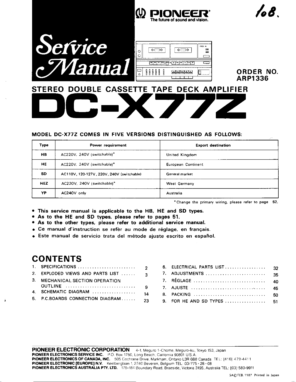
Page 1
[o'- r,6 1
o
o
t=FT;Tit F. |-T{=T;T-TT
E
8flflfl8fl
=Es-@=
E-
E=
:
ORDER
ARPl336
STEREO DOUBLE CASSETTE TAPE DECK AMPLIFIER
DG-X772
/oE.
NO.
MODEL DC-X772 COMES
TyPe
HB AC22OV. 24OV
HE
SD
HE2
a
This service manual is
a
As
to th6 HE and SD types,
a
As to the oth€r typ€s,
AC22OV.
AC11OV, 12O-127V
AC22OV,
AC24OV only Australia
Ce manual
Este manual
a
2 4OV
24Ov
d'instruction
de servicio trata del m6tode
IN FIVE VERSIONS
Powea roquiromont
(swatchable)'
(swrrchable)*
,22OV ,24OV
(
switchable)
applicable to the
please
refbr
se
CONTENTS
1.
SPEC|F|CATTONS ......
2.
EXPLODED VIEWS AND PARTS LIST ....,.
3.
MECHANICAL
IN
OUTL
SCHEMATIC DIAGRAM
4.
P.C.BOARDS
5.
SECTION OPERATION
E
CONNECTION DIAGRAM......
DISTINGUISHED AS FOLLOWS:
United
European Continent
(switchabl€)
"
General market
Wast
HB, HE and SD typ6s.
please
refer to
pages
51.
refer to additional service
mode
au
de r6glage, en
ajuste escrito
2
9
14
6. ELECTRICAL PARTS LIST,
7, ADJUSTMENTS
7. REGLAGE
7.
AJUSTE
8. PACKING
9. FOR HE AND SD TYPES
Exoon dostination
Kingdom
Germany
change the
manual.
franqais.
en espafrol.
primary
.......
wiring,
please
refer to
page
35
40
45
50
5l
PIONEER ELECTRONIC CORPORATION 4-1. r\,4esuro 1
PIONEER
PIONEER ELECTRONICS OF CANADA, lNC. 505 Cochrane
PIOI{EER ELECTRONIC
PIONEER ELECTRONICS AUSTRALIA PTY. LTD. 178-184
ELECTRONICS SERVICE lNC. P
IEUFOPEI
N.V. Keetberglaan 1.2740
O. Box
1760.
Lono Eeach Ca
Bo!ndarv Road. Braesrde. Vrctofla3195. Australia TEL:
N4arkham,
dnve.
Beveren, BelgrumTEL 03/775 28.A8
chome, r\y'esuro,ku, Tokyo ts3, Japan
orn a 90801 U S.A.
Ontano L3R 688Canada
TEL:
14161
479 4411
580-9911
I03l
SAC)fEB
rc37 Pr'nled in
'apan
Page 2
1.
SPECTFTCATTONS
Continuous Average Power
Watts*
per
channel, min., at 8 ohms f rom
Output
is 27
40 Hertz to 20,000 Hertz. with no more
than
0.37" total harmonic distortion.
'Measured
Trcde Regulation tules on Powet
Continuous Power
40 to
1 kHz
1 kHz
Graphic equalizer trequency band .......... 100 Hz, 330 Hz,
Hum
PHONO ................ ...._......_..._._ 72
Hum and Noise
PHONO
Total Harmonic Distortion
15 Walts
o.20/o
Tape Deck
Systems
Heads ...................................
Motor ....................
Wow
Fast Winding Time ..............
pursuant
Output
20,000 Hz ......... 27 W + 27 W
(DlN)
(DlN
and Noise
................. ..... 68 dB/60
per
power)
music
(lHF,
(DlN
continuous
channel
Federcl
to the
33 W + 33
'1
kHz,
short - circu ited, A network)
(40
power
output
Ttade Commission's
Output
(T.H.D.0.3%
(T.H.D.
W
(T.H.D.
kHz, 10 kHz,
3.3
Power/5o mW)
Hz
to 20,000 Hz, 8 ohms)
..............
Section
.................
Flutter
and
4 track, 2-channel stereo
Recording/playback head x
Playback head x 1
DC servo 2 speed motor
No more than 0.13%
Approzimately 105
tape)
Claims
I
ohms)
1% 8 ohms)
50 W + 50 W
1% 8 ohms)
i7
No more than
Erasing
head x 1
(WRMS)
seconds
fol
dB
dB
dB
x 2
(C-60
Frequency Response
-20
Normal tape
CrO, ............ .. . . .
Signal to Noise Ratio
Dolby
Noise Reduction
Dolby
recording:
dB
NR OFF
B lype NR
Effect
ON
...
Hz
35
to 14,00O
Hz to
35
......................... 56 dB
...... More than 10 dB
'15.000
(at
Hz
Hz
5 kHz)
Furnished Parts
Operating
Turntable fegs
Instructions
.......................
parts
...........................................................-. 2
1
M iscellaneous
Power requirements
European model
U. K. model
Australian model .............. .
destrnation
Other
Power
European model ..........................
U.K. model
Other
1
Dimensions
Weight
Specilications and
out
Consumption
destination models .................. ..................... ... 210 W
(without
notice
due to imp@vement
models
AC 110/120-127l22O/240 V
........... ...................... 210W
360(W) x 190(H) x 283(D)
14-3l16(W) x 7-1t2\H) x 11-1l8(D) in
package)
design subject to
.................................. 6.8 kg
AC 220 V,
AC 240 V, 50/60 Hz
AC
(switchable)
possible
modtications with
Hz
50/60
240 V, 50 HZ
50/60
Hz
210 W
mm
(15
lb)
Page 3
J
llzl
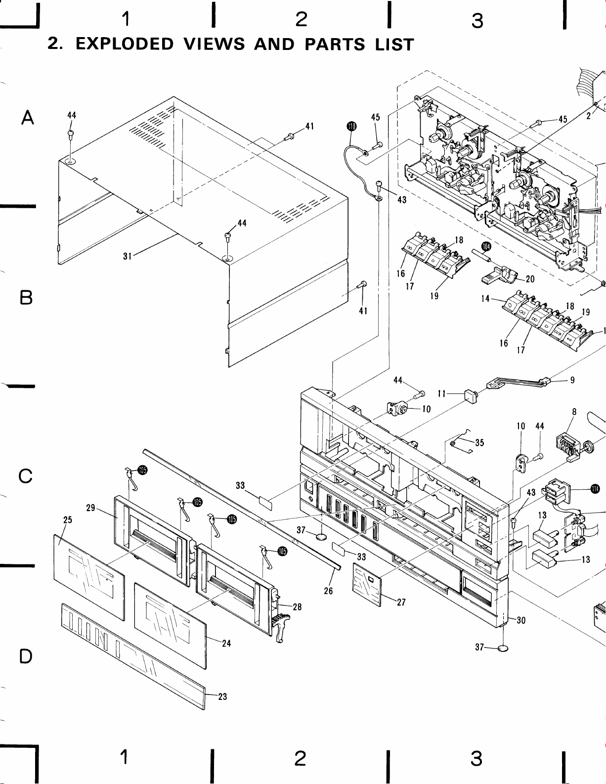
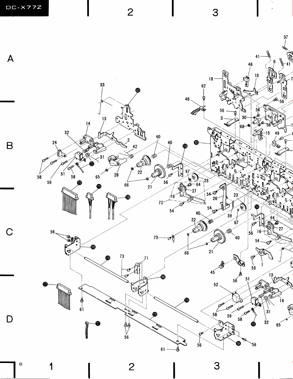
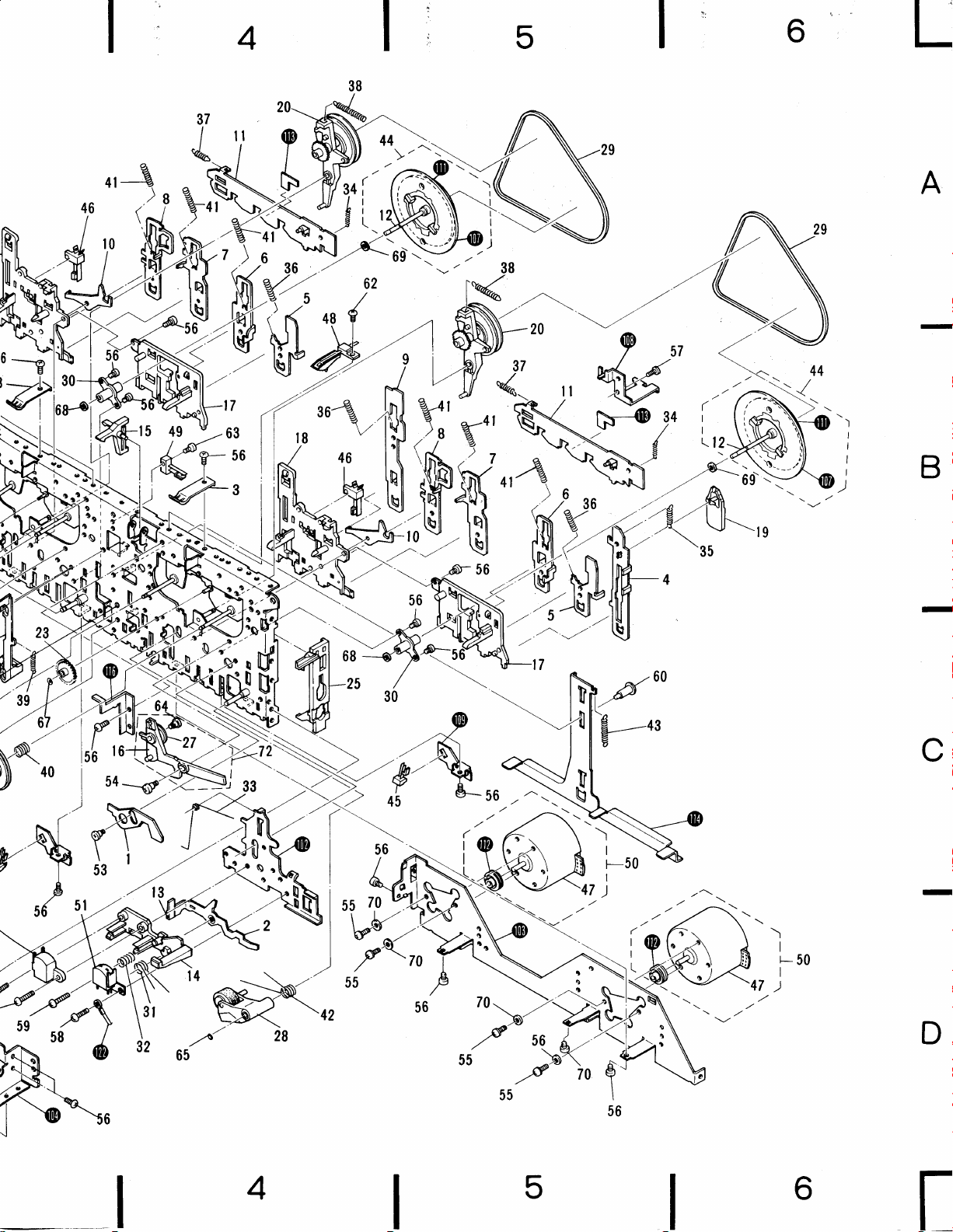
2.
EXPLODED
VIEWS
AND
PARTS
3
LIST
F\.'\
tt
,'\ \'.r
\t'ti
4"
N
YNI
1
2
3
Page 4
4
5
\>vt---'
i
i
1r''%i
6
L
A
t7
<4
f0
44
qzA
"
\:-x
B
'q
\
n"'oL"i'
B
c
4
44
2l
()\i
\.1
''o)Z,,
\Y
/'J
5
D
4l-
6
I
Page 5
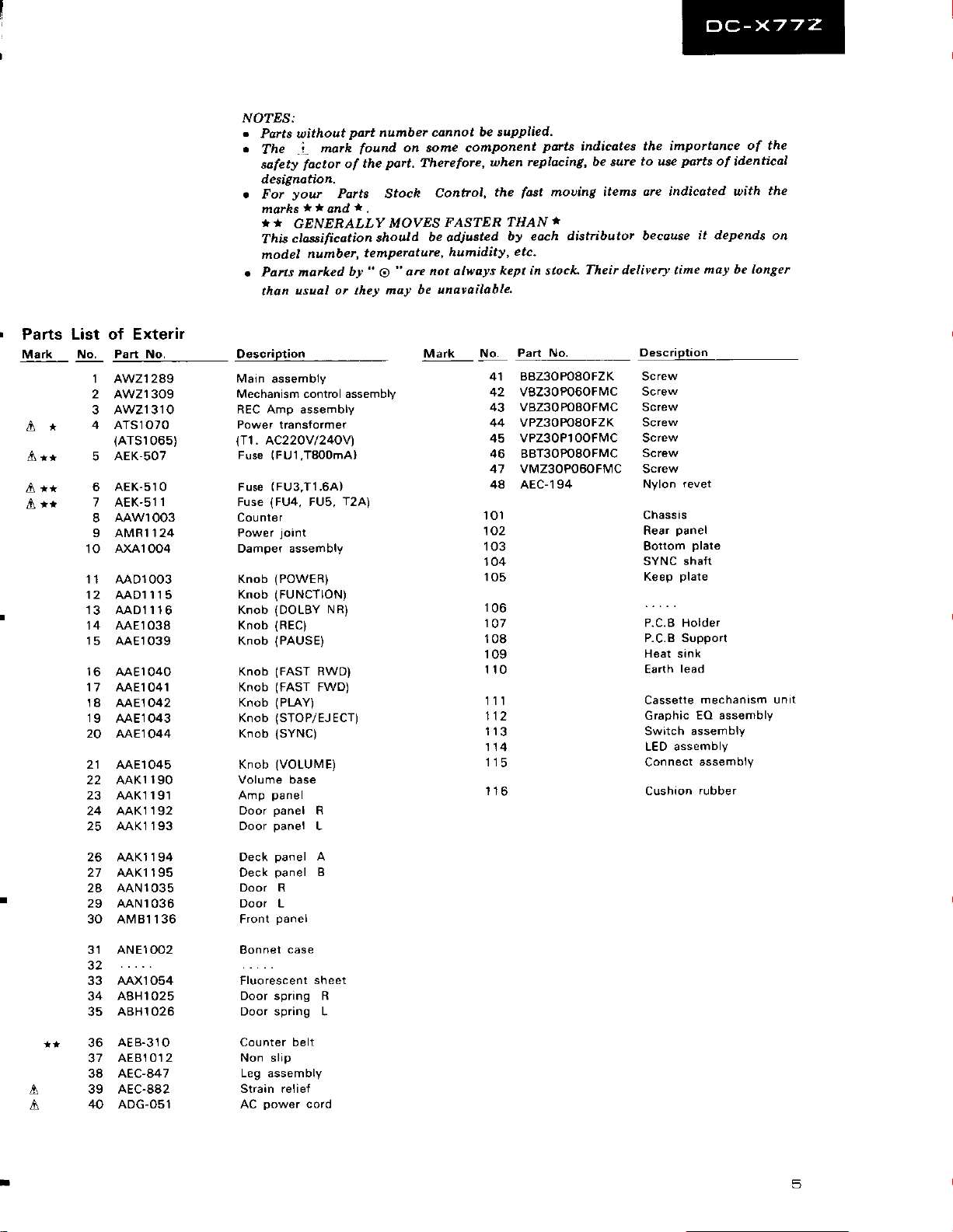
NO?XS:
.
Parts uithout
o
The
sofety
desEnotaon.
.
.
your
Fot
marks
**
CENERALLY
cld$ificatioa
This
model
Parts marked
than
port
morh
-i,
factor
A *
nutnber,
usual or lhe!
found
the
of
Potts Stoch
'l
ond
,
temperoture,
"
by
number con^ot
on aome compone^t
port.
Thercfore,
Control,
be odiusted
not always
are
unavailable.
FASTER
humidity,
MOVES
should
"
6
may be
be supplied
replocing, be 'urc
when
the
fast
THAN
b! eoch
etc.
kePt in sloclc
ports
indicotet
mouing items
*
distributot because
Theil delivery lime
the importonce
parts
to use
ate indicoted with
of identical
it depends
mat be longer
of the
the
orr
Parts List
Mark
A*
No.
10 AXAl004
11 AAD1003
12 AADl115
'13
14 AAE1038
15 AAE1039
16
17 AAEl041
18 AAEl042
19
20 AAE1044
21 AAE1045
22 AAK1190
23 AAK1191
24 AAK1192
25
of Exterir
Part No. Description
1 AWZI289
2 AWZ1309
3 AWZ1310
4 ATS1070
(Ars1065)
AEK-507
5
AEK-s10
6
7 AEK-s11
AAWl003
8
9 AMRI124
AAD1 1 16
AAE1040
AAE1043
AAK1 193
Main assembly
Mechanism control assembly
REC Amp assembly
Power transformer
l.11.
Fuse
Fuse
Fuse
Counter
Power
Damper assembly
Knob
Knob
Knob
Knob
Knob
Knob
Knob
Knob
Knob
Knob
Knob
Amp
Door
Door
^C22OV
/24OV)
(FU1,T800mA)
(FU3,T1.6A)
(FU4,
FUs,
joant
(POWER)
(FUNCTION)
(DOLBY NR)
(REC)
(PAUSE)
(FAST
RWD)
(FAST
FwD)
(PLAY)
(STOP/EJ
(SYNC)
(VOLUM
panel
panel
panel
ECT)
E)
R
L
T2A)
Part No.
No.
41 BBZ30PO80FZK
42 VSZ30PO60FMC
43 VBZ30PO80FMC
44 VPZ30K)80FZK
45 VPZ30P'r
46 BBT3OPOSOFMC
47 VMZ30PO60FMC
48 AEC-194
101
102
103
104
105
106
107
108
109
110
111
112
113
114
115
116
OOFMC
Description
Screw
Screw
Screw
Screw
Screw
Screw
Screw
revet
Nylon
Chassis
panel
Rear
Bottom
SYNC shaft
Keep
P.C.B Holder
P.C.B Support
Heat sank
Earth
Cassette
Graphic
Switch
LED assembly
Connect
Cushaon
plate
plate
lead
mechanism unrt
EO assembly
assembly
assembly
rubber
panel
26 AAKl194
27 AAKl195
28 AAN
29
30 AMBl 136
1035
AAN1036
ANElOO2
Deck
Deck
Door R
Door L
Front
Bonnet
panel
panel
cas e
A
B
32
33
AAX1O54
34
35
36
*t
37
38 AEC-847
A
A
39 AEC-882
40 ADG-Os1
1025
A8H
ABH1026
AEB-31O
AEB1012
Fluorescent
Door spring R
Door spring L
Counter be
Non slip
Leg assembly
Straan relief
sheet
lt
Page 6
A
B
2
3
g7
L
C
,-fA<
51
/
59
5'B
,*rP
W
)
65
fl
F
.t"
,n_-/Il,
56
I
116'
-
d
A
40
lh /'
45
$
2l
..t
,.'
,f
5
-
D
-l6
2
{l
*s>
3
J,
,/
N
f
Page 7
4
5
6
L
A
B
4
5
c
D
6
I
Page 8
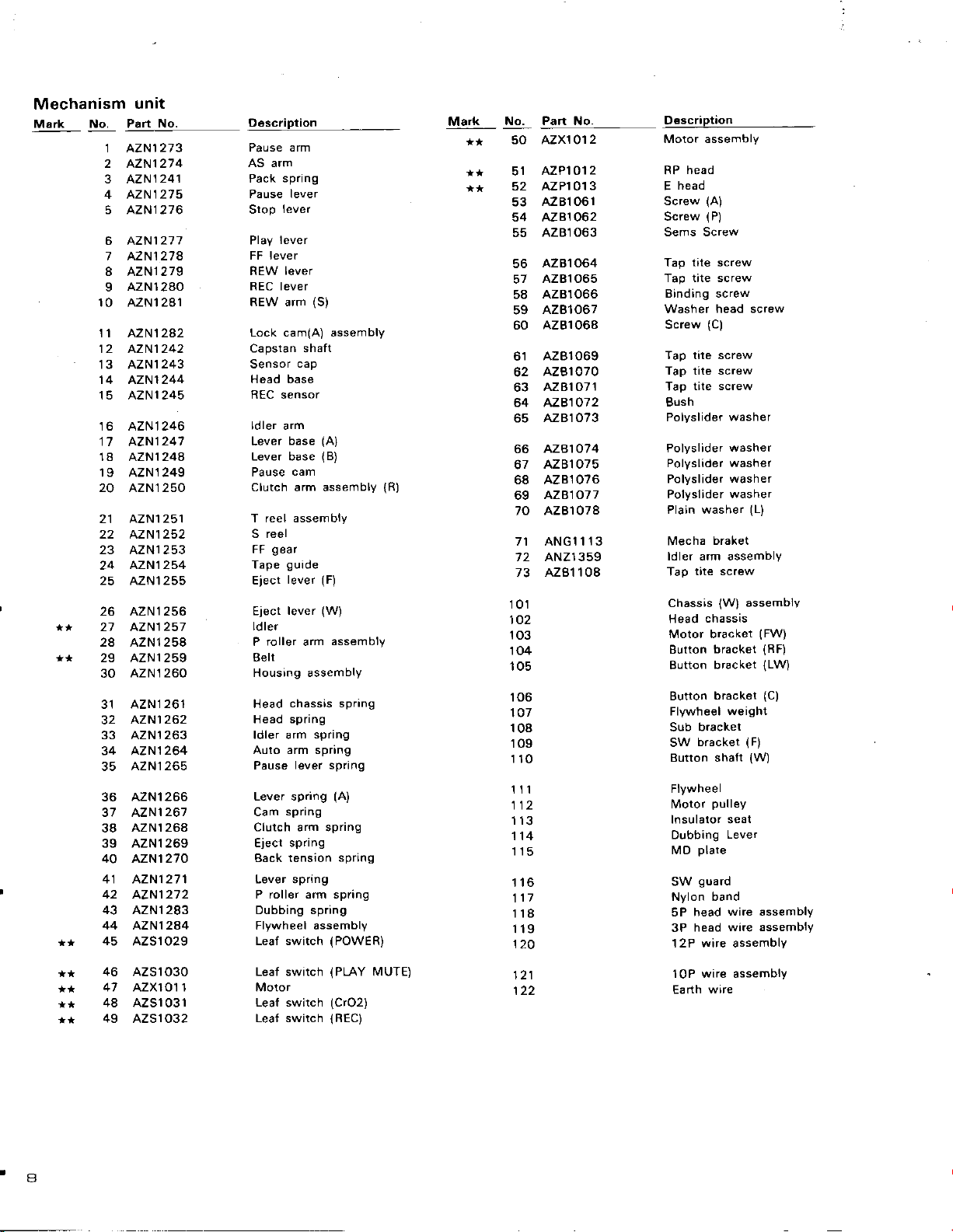
Mechanism
Mark No. Part
unit
1 AZN1273
2 AZN127
N'! 241
3 AZ
AZN1275
4
5 AZN1276
6 AZN1277
7 AZN1278
8 AZN1279
AZN1280
9
10 AZN't 281
1 1 AZN1282
12 AZN1242
13 AZN1243
14 AZN1244
15 AZNl245
16 AZNl246
17 AZN1247
18 AZNl248
l9 AZNl249
20 AZN1250
21 AZNl251
22 AZN1252
23 AZN1253
AZN1254
24
25 AZN1255
26 AZN1256
27 AZN1257
28 AZN1258
29 AZNl259
AZN1260
30
31 AZN1261
AZNI262
32
33 AZN1263
34 AZN1264
AZN1265
35
AZN1266
36
37 AZNl267
AZNl268
38
39 AZN1269
40 azN1270
41 AZN1271
42 AZN1272
43 AZNl283
44 AZN12A4
45
AZS1029
46 AZS1030
47 AZX1011
48 AZS1031
49 AZS1032
No.
Description
Pause arm
4
AS arm
spring
Pack
lever
Stop
FF lever
lever
REW
REC lever
REW arm
Lock cam(A) assembly
Capstan sh6ft
Sensor
Head base
REC sensor
ldler arm
Lever
Lever base
Palse
Clutch arm assembly
T reel assembly
S reel
FF
Tape
Eiect
Eject
ldler
P roller arm
Belt
Housing assembly
Head
Head spring
ldler arm
Auto arm spring
Pause
Lever spring
Cam
Clutch arm spring
Ejecr spring
Back tension
Lever spfing
P roller arm spring
Dubbing spring
Flywheel assembly
Leaf switch
Leaf switch
Leal switch
Leaf switch
(S)
cap
(Ai
base
(B)
cam
gear
guide
(F)
lever
(W)
lever
chassis spring
spring
lever spring
spring
{POWER)
(PLAY
{REC)
assembly
(A)
spring
MUTE)
(CrO2)
(R)
Mark
No. Part No.
50 AZX1012
AZPl012
51
52 AZP1013
AZB'I 06r
53
54 Az81062
AZB1063
55
AZB1064
56
AZB1065
57
AZB1066
58
AZB1067
59
60 AZ81068
AZB1069
61
AZe1070
62
AZB1 OT
63
AdB107
64
AZB1073
65
AZB1074
66
AZ81075
67
68 AZ81076
AZB1077
69
70 AZB1078
71 ANG1 1
72 ANZ1359
AZB1 108
73
101
102
103
104
105
106
107
104
109
110
111
112
113
114
115
17
18
19
20
121
122
l
2
13
D€scription
Motor assembly
head
RP
head
E
(A)
Screw
(P)
Screw
Sems Screw
tite
Tap
Tap tite screw
Binding scrow
Washer
Screw
Tap tite screw
Tap tite screw
Tap
Bush
Polyslider
Polyslider
Polyslider washer
Polyslider
Polyslider
Plain washer
Mech6
ldler arm assembly
Tap
Chassis
Head
Motor bracket
Bution
Button
Bufion
Flywheel
Sub
SW
Button shaft
screw
head screw
(C)
tite screw
washer
washer
washer
washer
(L)
braket
tite screw
assembly
{W)
chassis
bracket
bracket
pulley
Motor
lnsulator seat
Dubbing
plate
MD
guard
SW
Nylon band
5P head
head
3P
12P wire assembly
10P wire assembly
wire
Earth
(FW)
bracket
bracket
bracket
(RF)
lLW)
(C)
weight
(F)
(W)
Lever
wire assembly
wire assembly
a
Page 9
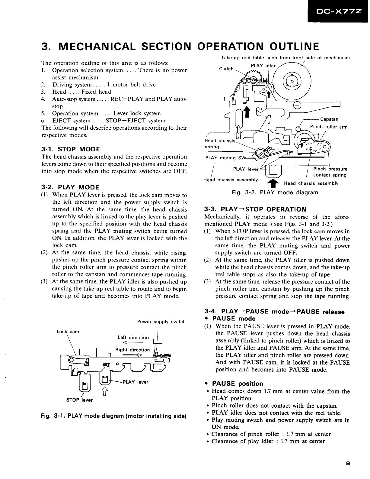
3. MECHANICAL SECTION
The operation outline of this
l.
Operation selection
assist mechanism
2. Driving system.....
3. Head.....Fixedhead
4.
Auto-stop system.....
stop
5.
Operation
6. EJECT system..
The following will
respective modes.
3.1.
STOP
The head
levers come down to their specified
into
stop mode when the respective switches are OFF.
3.2.
PLAY MODE
(l)
When
the
turned
assembly which
up
to the
spring
ON.
lock
(2)
At the
pushes
pinch
the
roller
(3)
At the
causing
take-up
system. . . . . Lever lock system
. ..
describe
MODE
chassis assembly and
PLAY lever
left
direction and the
ON.
specifred
and the PLAY muting
In
addition.
cam.
same time,
up
the
roller
to the
same time,
the take-up reel
of tape and
is
At
the same
is linked
the PLAY lever
pinch
arm to
capstan and
the PLAY idler
unit is
system . . . . . There is
I motor
REC+PLAY
STOP-EJECT system
pressed.
position
the head
pressure
becomes into PLAY mode.
belt drive
operations according to their
the respective operation
the lock
power
time, the head
to the
with
pressure
commences tape running
table to rotate
follows:
as
power
no
and PLAY auto-
positions
play
switch
chassis. while rising
contact
and become
moves
cam
supply
the head
is locked with
contact the
is also
switch is
chassis
lever is
pushed
chassis
being turned
spring within
pinch
pushed
and to
begin
the
OPERATION
to
up
Take-up
Head
chassis
spnng
PLAY muting
chassis assemblv
Head
reel table seen
PLAY idler
SW
PLAY
lever
Fig. 3-2. PLAY mode
3-3. PLAY-STOP
Mechanically,
mentioned PLAY
(l)
When
the left
same
supply
(2)
At
the same time,
while
reel table
(3)
At the same
pinch
pressure
it operates in reverse
mode.
STOP lever is
direction and releases the PLAY
time, the PLAY muting
switch are turned
the head
roller
chassis comes down, and
stops as
time,
and
capstan by
contact spring and
OUTLINE
front side of mechanism
Head chassis
diagram
OPERATION
(See
Figs.
3-l and 3-2.)
pressed,
the PLAY idler is
also
release
the lock
switch
OFF.
the
take.up of tape.
pressure
the
pushing
stop the tape
Capsta
Pinch
roller
Pinch
contact
assembly
of the
moves
cam
lever. At
and
pushed
the take'up
contact of
up
the
n
arm
pressure
spflng
afore-
in
the
power
down
the
pinch
running
STOP lever
Fig.
3-1. PLAY mode
Left
Right
diagram
(motor
Power supply
direction
direction
installing side)
switch
3-4.
PLAY-PAUSE
o
PAUSE
(l)
When
the PAUSE
assembly
the PLAY
the PLAY
And with
position
o
PAUSE
.
Head comes
PLAY
.
Pinch roller
.
PLAY idler
.
Play muting
position
ON mode.
.
Clearance
.
Clearance
mode
the PAUSE
(linked
idler and PAUSE
idler
PAUSE
and becomes into
position
down 1.7 mm
does not
does not
switch and
pinch
of
play
of
lever is
pushes
lever
pinch
to
pinch
and
cam, it is locked
contact with
contact
roller :
idler
mode-PAUSE
pressed
down
roller)
roller
PAUSE mode.
at center value from
power
1.7 mm at center
mm
: 1.7
in
PL,AY mode,
the head
which is linked
arm. At the same
pressed
are
at the PAUSE
the capstan"
with
the reel table,
supply switch
at center
release
chassis
to
timg
down
the
are in
Page 10
o
PAUSE
(2)
Nexg
PAUSE
(l).
the PLAY
release
when
the
cam is released
The
PLAY
mode
PAUSE
idler
and tape running
lever
in the movement
pinch
and
pressed
is
roller
then
recommences.
again,
reverse
return
the
to
to
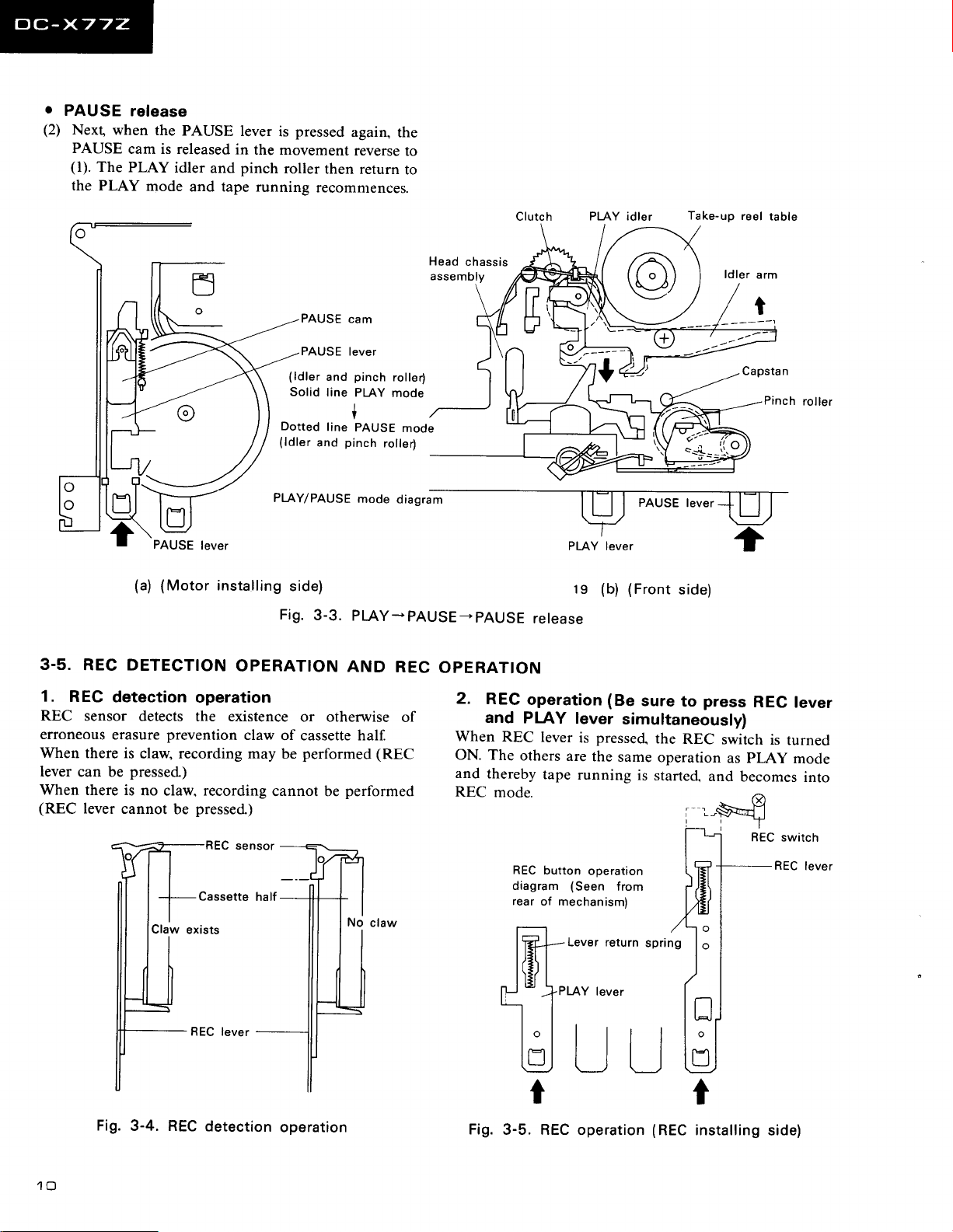
3.5.
(a) (Motor
REC
DETECTION
F
PAUSE
PLAY/PAUSE
lever
installing
OPERATION
PAUSE
AUSE lever
(ldler
Solid
Dotted
(ldler
side)
Fig.
3-3.
Head
assembly
cam
pinch
and
line
line
and
pinch
roller)
PLAY
mode
lt
PAUSE
PLAY-PAUSE-PAUSE
AND
roller)
mode
mode
diagram
REC
OPERATION
chassis
ts
release
PLAY idler
(b) (Front
Take-up
side)
reel
ldler
Capsta n
arm
t
Pinch
table
roller
1.
REC
REC
sensor detects
erroneous
When
there is
lever
can be
When
there is
(REC
lever
Fig.
detection
erasure
prevention
claw, recording
pressed)
no
claw,
cannot
be
3-4. REC
operation
the existence
claw
of cassette half
may be
recording
pressed)
REC
Cassette
detection
cannot be
operation
or otherwise
performed (REC
performed
of
2.
REG
and
When
ON. The
and
REC
REC
thereby
mode.
JB!,-Y
--t
Fig.
3-5. REC operation
operation (Be
PLAY
others
REC
diagram
rear
r_-l
Il5ff
lever
lever
tape
button
of mechanism)
pressed.
is
are
the
running
ooeration
(Seen
Lever return
'ever
I
tij
t_r
t
to
press
sure
simultaneously)
the
REC
switch
same
from
operation
is
started"
as
and
/
sprins
r_l
t
(REC
installing
REC
tever
is
turned
pLAy
becomes
REC
side)
mode
switch
REC
into
lever
Page 11

3-6. REC
Function
PAUSE
(r)
(2)
3.7.
(l)
(2)
same
-
PAUSE RELEASE)
-
REC
REC
SW and PLAY
PAUSE
REC function
REC-STOP
When
STOP lever is
lever
and PLAY lever
and REC lever
the REC
OFF.
The
other
operation
-
PAUSE
to the
PAUSE
_
PAUSE RELEASE
starts
-
description in item
SW
again.
OPERATION
pressed
are
returned
are
switch
and PLAY muting
operations
are the same
PAUSE
except for the followings.
keep
and the locks
released
by the return
RELEASE
(PLAY
5
REC
condition.
of REC
the PLAY lever
spring
switch
are turned
as PLAY-STOP
and
Stop mode
clutch
-
Reel
arm spring
gear
FF
sear
{
Clutch
arm
clutch arm orotrusion
diagram
gear
F/R
Supply
)
reel
Power
gear
supply
switch
-\--
cam
-
Lock
_JL
3-8. FFIREW
o
FF
operation
(l)
When the FF lever
(2)
o
(l)
(2)
REW
direction,
is locked
At
becomes
F/R gear
engages
the
operation.
Lock
lever
ON
At the
linked
direction
F/R
nearing
gear
rotate
the
with the lock
the
same
in
is
the F/R gear
reel
begins
operation
cam moves
pressed"
is
and is locked
same
to the
the
gear
is
the
with
the
and
becomes
OPERATTON
pressed
is
power
supply
time,
free
state
moved
time, when
simultane-ously
supply
by nearing
to rotate
in the
the
with
REW lever, pushes
protrusion
reel
supply reel
into
cam.
protrusion
the
due
with
left
power
the lock
the
of the
gear
gear.
REW
switch is
to the
FF
and
direction
supply
REW
lock
cam moves
shape
it
to the
gear
(reel
becomes
when
switch
cam.
arm
clutch arm.
moved in
and
engages the F/R
Then
the reel
operation.
turned
of
clutch
of FF
FF
gear).
(S),
in
to the
the
in left
ON and
arm
lever.
gear
and
Then
into
FF
the REW
is turned
which
left
Then
the
direction
begins to
(a)
STOP
REW
is
(b)
mode
REW
FF
mode
diagram
REW lever
mode
agram
/\
1,\0
,.'
\'1
C
!q-l
JHI
itot I I
-u
!l(tJl?....1
FF
(c)
,R
t'k
/1.
'r:t
ttl
----)
lever
FF mode
?
E
:
E
ILJ
til
r-5'r
.Y
ti
lFJ-
l(
r
3-6. FFlREW operation
Fig.
(Seen
from rear of mechanism)
(Motor
installing side)
Page 12

3.9.
AUTO
After
the
tape
playback
operations,
the linking parts
become
(l)
(2)
(3)
(4)
into
STOP
Auto
sensor
the
tape
end
At
the
same
AS
arm.
At
the
same
flywheel,
lever,
the lock
and releases
Thereafter,
REC-STOP
From
front
(Cassette
half
STOP
has
OPERATION
been
taken
the
auto sensor
release
the
mode.
becomes
time,
time,
lowered
the auto
the
auto
cam
PLAY
perform
they
and PLAY-STOP.
side
of mechanism
existsl
Auto
sensor
up
lock
arm
arm
shifts
lever
the
by the
cam
by the
is
contacts
toward
and
same
psta
Ca
recording
detects
and
the
tape
pushed
REC lever.
operations
n
them.
Then
operations
tension
up
by
the
claw
releasing
and
of
the
of
of
as
3-1O.
In
always
STOP*EJECT
case
go
operation.
Solid
line
Dotted
lines
PLAY,
through
denotes
denote
(Rear
REC,
FF
STOP mode
STOp
moqe
during
side
surface
MECHANISM
and
REW
lever
before
EJECT
operation
Eject
of mechanism)
enterins
It is
lever
lever
are locked.
EJECT
mechanism
on
the right.
ejecl
Fig.
3-7.
AUTO
and
(Cassette
Arrow
shifting direction
Auto
AS
PLAY
half
points
sensor
arm
lever
E head
STOP linkage
playback)
exists)
to
R/p
head
diagram
.'----_==-X..tlywheel
Capstan
/
6,1
Pinch
roller
(Recording
\
.-""*
"".
Auto arm
\
\\
'\
lj
(A)
Right
side surface
(B)
Motor installing
surface
Stop lever
of mechanism)
side
Fig.
3-8. AUTO
(Partial
cannot
playback)
and
sections
be
seen)
STOP linkage
of
auto
arm,
flywheel
diagram
(Recording
and
AS
arm
Fig.
3-9.
STOP-EJECT
mechanism
121
Page 13

3.11.
(l)
ONE TOUCH
STOP-One
Since the
mechanism,
to set
the P mechanism
mechanism
lever.
Moreover,
returns
differing
to the
completion
touch
PI-AY
and REC
into
REC mode
stop
of the
DUBBING
dubbing
levers
from
operation.
of P
lever
into
other levers,
position
OPERATION
operation
mechanism
are interlinked,
PLAY
pressing
by
without
mode
only
the
and
possible
it is
and R"/p
the dubbing
dubbing
locking
Vp
lever
after
(2)
Dubbing-STOP
After
completion
completion
STOP
function
possible
only upon
Moreover,
the
course
respective
Thereafter,
and
REC-STOP
operation
playback
of
of recording
of the individual
take
when
suspending
of
operation,
mechanisms.
the
operations
operations.
of P
mechanism
of
R/P mechanism,
mechanisms
up completion
the
dubbing
press
the
STOP levers
are same
as PLAY*STOp
and after
becomes
of the
operation
AUTO
tape.
in
of
R/P
mechanism
R/P
mechanism
R/P
STOP lever
mechanism
PLAY lever
Fig.
One touch
Solid line
Dotted
3-10.
dubbing
denotes
lines
REC lever
Dubbing
One touch
(Motor
denote
installing
operation
STOP mode.
during one touch
lever P
dubbing
side)
diagram
mechanism
operation
dubbing
operation
P mechanism
STOP
(1)
PLAY lever
lever
P mechanism
,1
2t
Fig.
3-11.
One touch
dubbing
operation
(2)
to
Page 14

2
3
4. SCHEMATIC
DIAGRAM
MECHANISM CONTROL ASSEMBLY AWZI3O9
cr,r
!
^li
-
o&!-6oorMoroR
coNTRoL
I
|
ELRA
I
3
Page 15

o2o7,2O8: HrGH SPEED SrTCH
o2@.2ro:TAPE I SWTTCH
02il.212:TAPE2SW|TCH
O2t3.2I4:PB
MUTING
5
6
tl
L_
o221,
R?.zs
fr:Ll
)2€
.
a2t7,214
FILTER AMP
02t5,216
:
ALC
DOL€Y
rol5o
V R535
4
tczo1,2o4,ez27-zz9t
'i
s
5
0232-236 Brasosc
R!i9
6
I -J
I
REc
t_
Page 16

7
I
REC AMP
IC5Ot:
H|GH SPEEO
osostsi
I
SWTTCH
czao
c279
|
,sE
i
a, t-@
vR2o7l
I
47or - 47ok
i336
vF2q
ilechanjsn
s60z/0603
0604-0606
a601
D6o2
D601,0604
vR6O1
VR602,VR604
Contort
,VR60l
F537 220
AssembrY
2SA933S
2SC1740S
2SC337l
Ro6'2Esn
1ss1ll
vRlF6H102
vRld6H202
REC
IC50l
!c502
s501-a504
a505-0508
0503
0501
1501,1502
R5!s-:?'{fll
,5r
Amp Assenbly
.D502,0504
rnducto.
'"1
| | |
stlTcB
s201.s202
a??5
D??6
O5O7,3OA:
tcm2 : cr&
AssemblY
NORMAL SPEED SWTCH
EO
AEL.44]
AELIO]J
I
7
8
I
Page 17

GRAPHIC EQ ASSEMBLY
(I/2}
11
tc4o!,4o2:
GEO AMP
c4i9
0.15
/10
12
MAIN ASSEMBLY
I
r+
1i
F-r
ilr
"l
_d_
'EF
AWZ12A9
rcloiiPHoilo
12/21
Eo atP
rcl02:
BUFFER I. MIX
AMP
,10
11
TUNER
12
rcto4, !05:
REGU
Page 18

.l?
t\,
14
15
frain Asserbty
rc201
r c202
rc101.rc102
IC103
r c203
tc204,Ic205
rc104
rc105
422 6
0
1
2 0
O 2 0 2 . 0
2 0 '
.
a2?9,0231
.a?32
s 2l0
0234
a101
o 1 0 2 , 0 1
0 I , a 2 0 9 - o 2 1
a???
,a??1 ,a227
0217,A218
a104,0235,q216
0203,a204
01 10
Dl OE
0102-0107
01 01
s101
RYlO]
s102
t ?D1
20?
.F
1101,1102
L?05,1206
!203,1204
TZOl
L2O1,t202
1207
c27 A
cl45,C116
c135
c137.C13A
vR101
-VR206
vR201
vR207,VR208
-
o
o
2 0 6
.
0 2 1 9
6
,
.92?8,a233
2 ? 3 , D
-
gat416BL
HA12O86NT
il5?16P
tc4001BP
1C4069U8P
UPCTE[123
!Pc78128
DTA124ES
(
r
1
2 q E
5
Dtct4lEs
2SA9lls
2SBE34
2 S C 1 7 4
0 S
2SC1740SLN
25C3377
2SK573
Hls15L
RDl3EB
s5566
ASG1005
(ASG1007)
ASR1005
(ASR-111)
suJ8L22224L
ATF-?10
ATH-133
ATn-037
ATil1OO1
aTx-035
LAU?21K
LTAlO2J
ACE-1
34
ACG1002
ACG1005
acut
002
vRTil6V20l
G.aphic ES Assenblt
IC401.rC402
vR401-VR405
0401-D404
BA]8121
ACU1011
RDlOESB
RESISTORS:
Indrcated In
nored k; t0, M; Mn.
CAPACITORS:
Indrcated In
Indrcarion
VOLTAGE,
f:li
E,
€
@l;
OTHEAS:
The-A
fte safery facior
pans
N
The undenrned
This rs the
rmprovemenis r.
SWITCHES:
THE UNOERIINED INDICATES
s101 P09ER
s102-1 PH0N0
s102-? cD
s102-l vtDE0
s102-4
S102.5
Sritch
sz0- DoLaY !F
s202
1/4W.
Q,
1/6w
(F)j
a1%.
(pF)/volrage
capacity
w(hout voltage rs
CURRENT:
Sisnal vohase ar 30 w + 30 w,
(V)
Dc vohage
raled
mA
DC curenl at no ,npur
Slsnar vollase ,t FM 4oO Hz t 75
S,snal .o!le.
;
i>
Adtwtire
I
A
ma,k
rdentical
ot
marked
at no Inpul
powei.
potnl
lound
on some component
pan.
of lhe
designanon
capacitors and resistors have
Indicales the
basic schemarc d'egram,
des19n.
TUrER
TAPE
Assenbty
Hj-SPEED oN-QII
1/8W
and
J5% tote.ance lntess otheturse
t2%,
r1o%.
8a ourpui
kHu DEV
Ind'Lares
pans
.umbers.
F F
a2o% rote.adce
{M)j
(1
kHzl
(
,s DC voltase
)
rhe ,mponance
{G);
lK);
(V)
!nless otheMrse noted
50V ercept electrotyric capactror.
sisnal Valle In
s,gnal
pads
The.elore,
when replacing, be
positron.
swnch
bur the actual crrcuil may vary due ro
THE SWITCH POSITION
-_91,L
0 N
!!-0
-_91_!
0 N
--Qlf
N
0
-.911
N
0
N--qr[
0
0\-0.1
sure
p: pF.
ro
ar
o'
use
DCl?V
OUTPUT
GRAPHIC EO ASSEMELY
I2l2)
PHONES
F,]M;---__-l
wi..
sP- oded
I
:
rw
I
-l
L
J
-l
R
Aac
AOG-051
SPEAKERS
powen
F;,;l
ac240v
5O/6OH2
cono
2
13
14
L----J
T! PowER TRANSFoRMER
A
ats ro70 r ATsio63t
I
15
Page 19

16
17
I
I
I
NOTE:
The indicated
only. Other alternatiue
are listed in
semiconductors
parts
the
are
semiconductors
list.
representatiue ones
may be
used and
External
2SA933S
2SC17405
2sctz+cuN61
Appearance
1'o'No-f\SI1'l
*1ffi"'*

B
llrl
P.C.BOARDS
CONNECTION
3
DIAGRAM
F
1
2
3
Page 21

rl
5
6
ctta
atu
a-
o
tr
aDa
o8
tctor
ClOl
cta
cttt
rctol
ctto
otaa
e''
clol
rctot
c22'
cttt
octo -ra
ctta
cltl
rctoa
rcto.t
.Cta
cto
ctrt
ctto
ctot
caa
ctll
tc-a
att
ctat
et.
atll
at
C'
rr?
I{
4
5
6
Page 22

o|oa oios
7
REC
AMP ASSEMBLY
8
AWZI3IO
rc
30t
olor
O22t
o22l
rc203
o230
o22t
o2a2
O2Ol
o222
o223
o220 0at9
o221
Q22l
rc205
rc204
o254
o20l
Q2t2
o 2ro
O2t5
o2l
O2O2
tc20r
i
o20f
o2i5
02l
o2l
o2rt
o217
4
I
o2rc
CASSETTE
|
*ar^*, ",
xEcilirtt
I
ll
MECHANISM
ASSEMBLY
MECHANISM
tl
L ci
+
ici
Er^sE
i
CONTROL
AWZt309
ASSEMBLY
REC
Cr
O2
XUTI
NOTE
1. Thir P.C.8
2.
t.C.8.
Th.
wirh
paa
dr.
p.srn
EO
cffapq|dint
7
ffidid
hia
*rich
di.arh indlc.llo
OSOI
a
O O
o-o2o3-o
-o
0-12!7
/c513 \
@'.
i
Ecs|lE
Oth.r3
t.C.B.
panain
diat.m indicatior
tc
s
FY
L
F
VR
3.
Th.
cOeitq frfrind m*t.d witho(&!U.
L
Th. diod. mind
5.
Th.
tr.di.td tmin.l ro whkh
m..td wlth
di{..m b viMd f.6
b-n |dntd on tfr lbdd o ba nplac.d with
ririrt
rymbolr
Cdiioo(tnf
pd
nontad.id..
tti
ll.i.d in th. tolbri|rr T$L.
pan
rymbol
fHl':fgl
P]ffir
D20l
o---{a<
R257
rVVt-<
"#1"
'JF
Prt
Nm
tc
gf,iictt
F.l.y
Coil
Filt.l
VatiabL radator
S.mi-flx.d
ldo.rt||
O
E i. .fflx.d dffi th. .mittf,.
or
cblol
circl-l .h{ n
circlil $w o'tod. .kt .
tliv.
thd Ailn
PmNm
T.a6iabr
F.dilor typ.
tr6iabr
Diod.
R6irtor
Capacitor
(PohriW)
C+-itor
(Nd{oLritV}
tmi.d.
I
7
I
I
9
Page 23

6.
ELECTRICAL
NOTES:
.
o
wilhout
Parts
Parts marked by
part
number connot
"A"
able.
The
mork
A,
found
replacing, be sure to use
your pans
For
' *
GENERALLY MO'ES FASTER THAN
Stock Control, the
This classifcation shall be
When ordering resistors,
Ex. I When there are 2 elfective digits
5'%.andK: I0'b.
5fl9 56x101 56,t..........................RD1/1PS66[ll
17kQ
47xt0t 173..........................RD1/4PS@A6J
0.54 0R5...............................................RN2HO88K
1!> 010................................................ Rs/P o t!
Ex. 2
When
there are 3 effective digis
'62k9 562x tqt 562t ........................ RN1/4SR tr 6 E E
Miscellaneous Parts
P.C.BOARD
Mark
ASSEMBLIES
Symbol & Description Part No. Mark Symbol & Oescription Pan No.
Main
assembly
Mechanism control assembly
REC Amp
Graphic EO assembly
Switch assembly
LED
Connect assembly
assembly
assembly
PARTS LIST
b? supplied.
not always kept in stock. Their delivery time may be longer thon usual or they
are
on some
parts
component
of itlentical .lesig,nation.
fast
par$
moving
indicotes the impormnce of the
items are indicated
with
*
adjusted by each distributor because it depends on model
conve rcsistonce
frrst
(any
values into code
digit opaft
from
form
0), such as 5(fl ohm and 47k ohm
o K
(such
AWZl 289
AWZl 309
AWZ1 310
as in high
precision
metal
tt
*t
tt
*r
*r
the marks
as shown in the
0230
4234
0101
0102, O'l03, O209-O216,
0219-0222.
4224.4233
4217 , 4218
frlm
F
safety
factor
*
*
ond * .
number, temperature, humidiry, etc.
following
resistors).
4224, A227
pa
of the
examples.
(tolerance
may be unavail-
. Therefore, when
is shown by J
DTC! 43 ES
2SA933S
2S8834
2SC1740S
,
2SC1740SLN
-
OTH ER S
Mark
A
A
A
A
Main Assembly
SEM ICO N
Mark Symbol & O6sc.ipiion
A
Symbol & Dosc.iption
T1
r
r*
r*
r.*
Power t€nsformer
l^c22ov
FU'! Fuse
FU3 Fuse
FU4, FUs Fuse
AC
/24ovl
Power cord
DUCTO RS
lC2O1
*r
lC2O2
rt
lC1
at
r*
t*
1C102
01
,
|c103
IC203
tc204, tc205
rcl
04
tcl
05
4226
0201
0202, 0205-0208,
,
4223.4229-4232
(TSOOmA)
(T1.64)
(T2A)
(AW21289)
Part No.
ATS1070
(Ars1065)
AEK-507
AEK.51O
AEK.s1 1
ADG-051
Part No.
84341 6 BL
HA12086NT
M5218P
sTK414'l
TC4001 BP
TC4O69U BP
pPC78M12H
pPC7A12H
DTA124ES
DTC124ES
O1O4, 0235, 0236
*r
o2O3. A2o4
*t
D11O
r
0108
r
Dl02-D107
*
A
* D109, D2O1-D21O,
D213-0224, D227
D101
r
A
SWITCHS & RELAY
Mark
Ar*
Symbol & O€sc.iption
sl01 Push switch
RY101 Relay
5102 Push switch
(PHONO,
TAPE)
CD, VIDEO, TUNER,
-D240
lPowER)
2SC3377
2SK373
HZS15L
RD13EB
1SS131
4D4B'44
Parl No.
ASG1005
(ASG1007)
ASRl OO5
(ASR-111)
suJat22224L
Page 24

COILS, TRANSFORMER
Mark Symbol
F2O1 , F2O2
L101, L102 AF choke coil
1205, L2O6 Trap coil
L2O3, L2O4 Trap coil
T201 Bias OSC translormer
1201, L2O2 Inductor
L2O7 lnductor
Do.cription
a
DOLBY Filter
CAPAC ITORS
Mark
Symbol & Dosc.iption
(680PF/630V)
c278
C145. C146
Cl35
C137, C1 38
c209,
c101.
cl19. C] 20,
c207,
(O.01pF/AC125V)
pFlAC1sOV
{0.01
\33OOpF/a2vl
c210
c102. cl05,
C203. C204.
c204. c215,
cl53. C154
c279. C2AO
7
c27
c147,
C1
4A
ct 28
c127
c123. C1 24
c129
c134
c269
c249. C250
c117,
C11a. C213,
c235. C236.
c136. C243.
c256,
C257
C244,
C261. C262,
c267, C270
c140.
c125, C126
f1t1 f1)) aa11
c1
41
C't 43.
,
c251 . C252
c224,
C241. C242,
c2 59
cl30
c133, C217,
c239.
C21a. C225,
C240
c139
cl13. Cl 14,
c221.
c264. C26a,
c107.
c142, C271.
C223. C226,
C237. C238,
C283, C284
c108. c1 15,
C272
c260
AND
C106.
C216.
c2't
,
c2
c144
c234,
c258.
C263.
16.
C1
FILTERS
)
4.
66,
Part No.
ATF-210
ATH.133
ATM.O37
ATMI OO1
ATX.O35
LAU221 K
LTAl
02J
Part No.
ACE-134
ACG1002
ACG1005
ACH-249
cccsL100 D50
cccsLl01
J50
cccsLr 0l K500
cccsL221J50
cccs 1470J50
Pl
CEAN
CEAN P22O M50
CEAN P33O M25
CEANP4TO M50
cEASR4T M1
CEASR4T M5O
CEASR6S M5O
cEASO10M50
CEASl OOMSO
CEAS101
cEAS101 M25
CEAS2R2M5O
cEAS220M't 6
CEAS221M1O
CEAS221 M16
cEHAO332
CEAS4RTM5O
cEAS470 Mr 6
CEAS471 M16
OO M50
00
M1 6
M25
Symbol & Descriprion
c245, C246,
c213. C274
c2aa
c247,
C24A,
c221 , C222
c219,
c103,
c231 , C232
c253. C254
R ESISTO RS
Symbol
vR1Ol
R166, R167 RD1/2 PMFL1
R168, Rl70, R171 RD1/2PMtrtrtrJ
R149, R150, R152-R154 RDl/4PMFLtr D OJ
R155, R156, Rl69 RD1/4PMFtr D !J
R145-R148, R151. R159. RD1/4pMtr ! DJ
R1
60,
Rl 62 RSl LMF51 1J
R164, R165
VR201-VR206(20k
VR207.
Other resistors
OTH E RS
M6rk
Mechanism
Symbol & Doscription Psn No.
Jack 6P
Terminal
(DCl20V
Jack
Control Assembly
SEMICONDUCTORS
Mark
Symbol e Description
0602, 0603
*t
0604-0606
tt
0601
**
D602
r
0603, D604
r
CAPAC ITO RS
Mark Symbol
c604
c601-c603
RESISTORS
Ma.k Symbol
vR6O1. VR6O3
vR6O2, VR6O4
Other resistors
c275, C276
C220,
c229, C230
c104,
c205, c206.
D€scription Part No.
&
(1O0kX2)
R319
VR2O8(5O0k Semi fixed)VRTM6V504
(PHONO,
4P
{SPEAKERI
Oosc.iption
&
Oescription Parl No.
&
Part No.
coMA103K50
cKcYX104M25
coMA153K50
coM4223K50
coMA273 K50
CEJAOl OM5O
CEJAl OO M1
ACU1O02
RS2LMFtr O OJ
lixed)VRTM6V203
Semi
RD1/8PMC
CD, VIDEO) AKB-Og5
OUTPUT) AKN-034
AKE-109
(AWZI
Part No.
2SA933S
2SC1740S
25C337 7
RD6,2 ESB
'|
ss131
Peri No.
3O9)
cEAS'r 00M25
cKCYX473 M25
(1k
(2k
fixed)VRTM6H
Semi
lixed)VRTM6H2O2
Semi
RD1/8PM tr tr trJ
102
6
OoJ
tr
trJ
c109. c1 1 0
c201
c202
,
c111, C112
c211. C212,
c131. C132,
c149,
C150,
c2a1 . c2a2
c151
c22a
cKcYBl 52 K50
cKcY8561 K50
cKcYB562 K50
cKcY868l K50
cKcYF473Z50
cKcYX473 M25
Page 25

R
EC Amp Assembly
SEM ICO NDUCTO RS
Symbol & Description
rc501
rc502
-0504
o501
o505-o508
D503
D501, D502. D504
cotL
Ma.k
CAPACITORS
Mark
R
ES ISTO
Mark
Symbol
L501, L5O2
Description Pan No.
t
Symbol & Description
c507. c508
c501 , c502
c521
c503, c504
c505, c506
c519, C520
c513. C514
c511,
C512.
c509, c510,
RS
Symbol & D€scription
All resistors
(AWZ1
Inductor
c515, C516
c517, C518
31 O)
Parl No.
M52181
M74LSo5P
2SC1740S
DTCl
R D5.6 ESB
1 SSI 31
LTA392J
Part No.
CEASR33 M5O
cEASO10M50
CEAS101
C EA54R7 M5O
cEAS470M16
coMA153J50
coMA223J50
coMA392J50
coMA822J50
Part No.
RD1/8 PM
24ES
M 10
tr tr
trJ
RES ISTOR S
Mark Svmbol & Doscription
VR401-VB4O5
r
r
VR406
(30k)
130kX2)
R407, R408
Other resistors
OTHER
Mark Symbol
Jack
Switch
Maik
Assembly
Symbol & Ooscription
5201, S2O2 Push swrtch ASG-424
r*
(DOLBY
Oasc.iptaon
&
(PHONES)
NR, Hi.SPEED)
Part
ACUI 01 1
ACUl01
RD1/2PM331 J
RDl
Part No.
AKN
Part No.
R ES ISTO R
M
ark Symbol & Description Part No.
R327
RD1/8 PM103J
LED Assembly
SEM ICON D U CTO RS
Mark Symbol & Description
D225
t
R
ESISTOB S
Mark Svmbol & D€sc.iption
R329
R328
Pan No.
AEL-443
AEL1O33
Part No.
RD1/8PM471J
RD1/8 PM681 J
No.
3
PM tr D OJ
/8
1OO7
Graphic EO Assembly
ICO
SEM
Mark
CAPACITORS
Mark Symbol
N DUCTO RS
Symbol & Description
lc4o1, lc4o2
rt
D401 - D404
&
c419,
C420
c42t, c422
c425.
C426
c401
c402. c427
,
c435
c423, C424
c403. c404
c433,
C434
c43t, c432
c409,
c410
c407.
c408
c4't 5, c416
c413.
C4t4. C429,
c411,
C412
c417 , C41A
c405, c406
c437, C438
Doscription
Part No.
843812 L
RDl
OESB
Part
No.
CEJARl SM50
CEJAR6SM5O
c42a CEJA4R7M50
.
CEJA1 Ol M1O
CEJA4TOMI6
cKcY8331 K50
cKcY839't K50
cKcY856l K50
cKcYF472250
coMA153K50
coMA182K50
coMA183K50
c430
coMA333K50
coMA392K50
coMA393K50
coM4682K50
cccsLl0l K50
Connect
No
supply
Assembly
part
inside.
Page 26

7, ADJUSTMENTS
Tape
l.
2. Turn
3. Mount
4.
5.
6.
7. Put
speed
Connect
(Dolby
Short-circuit
on the
adiustment
the frequency
TP:
L-ch)
the tape
the
tape
switch
test tape
between
assembly
mode.
(STD-301
Adjust
frequency
Release
TP5
and TP6.
the
VR60l
play
is
with
VR602
of deck
the short-circuit
deck
I into
so
that
becomes 30lOHz
(Note
l:
Be sure
ing
the
normal
speed
countr
on
the
on.
STD-301
terminals
and
backed in
so
that
I become
play
playback
the
+l0Hz.
not to
turn
adjustment)
to the TPI
complex
onto deck I.
TP4,
put
the deck
double
the
6020H2
between
mode
signal
VR602
assembly.
playback
terminals
and
while
terminal
TP5
and Tp6
I into
speed)
signal
+20H2.
adjust with
frequency
perform-
play
Tp4,
8. At
this
flutter
mal
speeds.
9. Mount
10.
Short-circuit
on the
mode.
(STD-301
11. Adjust
frequency
deck I.
12.
Release the
TP5
13.
Put the
VR603
deck
(Note:
the normal
14. At this
flutter
mal
speeds.
point,
are
be sure to
within
0.390 both in the double
confirm that the
the test tape STD-301
between
tape
assembly
play
is
with VR604
of
deck II becomes
short-circuit
terminals
and
backed
so that
put
in double
between
onto deck II.
TP4. TP5
the
deck II into
playback
the
+20H2
wow
and nor-
and TP6
speed)
signal
against that of
terminals TP4.
and TP6.
deck
II into
so
that the
II becomes
Be sure
not
speed
point,
be sure to confirm that the
play
playback
+l0Hz
to turn
against
VR604
adjustment)
mode
signal
and
frequency
that
while
adjust with
of
deck I.
performing
wow
are within 0.390 both in the double and nor-
and
play
of
and
(Note)
Short-circuit
(double
speed)
VR604
@ @
between
adjustment.
VR603
MECHAN
Tp4
VR6O1
@ @
ISM
CONTROL
and TP5
R60
,"ro,'Ho
I:r
during
tape
ASSEMBLY
AWZ1309
\rgrl
speed
VR2O3
@
Fig.
7-1
Adjustment
Point
Page 27

Electrical
Prior
to
firm the
system adjustment
the electrical system adjustment,
following itesm.
1. The mechanical adjustment should
2. Perform cleaning of the
tion of
The level
3.
=
head with the head eraser.
during
measurement is determined at OdBv
lV.
4. The specified tape should
the test tape has A side and
Since
with label.
side
STD-331B:
STD-608A:
For
Normal
STD-620: CrOz blank
Prepare the
5.
following measuring
AC millivoltmeter,
and oscilloscope.
ator,
For
6.
7. Turn the
the adjustment,
otherwise specified.
unless
Dolby
NR
head
and
be used for adjustment.
playback
system adjustment
tape
blank
tape
low frequency
perform
switch
both
to off
instruments.
oscillatore,
L and
specified.
be sure to con-
be completed.
the demagnetiza-
B side, use the
A
attenu-
R channels
unless otherwise
8. Prior to the
the set
ing the
quency
adjustment, be sure to
for
several
adjustment of the
characteristics, aging should be
REC/PLAY mode for
The-adjustment
9.
with
the adjustment order. If the order is not
it may
cause the
which induces
Deck I
Head
l.
2.
azimuth
Playback
level adjustment
Deck ll
l. Head
2. Playback level
3.
4. Adjustment
azimuth adjustment
Adjustment
of recording and
characteristics
of
minutes. Especially
recording
3 to 5
should be
failure
inferior
the
performed
of the complete adjustment
function of the unit.
adjustment
adjustment
recording level
perform
prior
and
minutes.
in
playback
aging of
to enter-
playback
fre-
performed
accordarrce
kept.
frequency
in
30s
3l5Hz
kHz lOkHz
6.3
315Hz
Fig. 7-2
Test tape
12.5
okH 8
kH2
STD-331 B
kHz
,3kH
3t5Hod B
lkHz
16Onwb/m
kHz
I kHz
2
OOHi
25H
;3 H2 lOHz
Page 28

AdjUStment
1. Head
Procedure
2. Playback
Procedure
1
1
azimuth
Tape
selector
(AUTO)
NORM
level
Tape
selector
(AUTO)
NORM
AdjUStment
1. Head
Procedure
2. Playback
Procedure
'l
1
azimuth
I
ape
selector
(AUrO)
NORM
level
Tape
selector
(AUTO)
NoRM
|
I
3.
Adilttmontlt tacotding
fruqu!.rcy
Procedure
1
2
3
'
Sefect the test
4. Recording
Procedure
1
2 NORM
3
chaaetarlldc!
Tape
selector
(AUrO)
NORM
NORM
NORM
lovel
Tape
selector
(AUTO)
NORM
CrOz REC/PLAY
Of DgCk I
adiustment
adiustment
Of DgCk
adiustment
adiustment
I
I I
PEC/PLAY
tape, tape
adiustment
REC/PLAY
*This
Mode
PLAY
Input
Play
on test
*
Perform
Mode
PLAY
Input
Play
on test tape
*This
II
Mode
PLAY
Mode
pt-lv
dd
Mode
REC
REC
Input
Play
on test
*
Perform
Input
phy
I
test tap6 sTp-3318
phybld(
Input
STD-6O8A
REC mode.
Apply
to the
the CD
Record
315H2
tape
selector,
Mode
and
'
Set the
Input
REC Apply
to the CD terminal
the
Record
31 SHz
sTD-608A.
Record
31
SHz to the test
sTD-620.
provided
deck is
signal/test
back lOkHz/-2OdB
tape
STD-3318
this
adjustment
signal/test
back 31SH2/OdB
STD-331B
deck is
signal/test
back 315H2/OdB
tape STD-3318
this adjustment
signal/test
back 3l sHz/odB on I vnzo+
'
This adiustm€nt is
cis€d not
signal/test
and
the signal
CD terminal
switch on.
play
and
lOkHz
and
STD-6O8
Dolby
NR
switch and satisfy the
graphic
signal/test
the
signal of 315H2
with
an auto-tape-setector mechanism.
tape
Adjusting
Head
adjusting screw
(Fig.7-3)
precisely
tape Adjusting
vR2O2
vR201
provided
with an auto-tape-setector
tape Adjusting
Head
adjusting
(Fis.
precisely
tape
|
Adjusting
vR203
p€rfom6d
to worcen rh€ distortion ratio
tape Adjusting
put
into
of 315H2
Bias
frequency
T201
Input
and turn
back
on test
equalizer and
tape Adjusting
VR2O8
VR2O7
balance volume to
Input
since this
7-3)
since this adjustment
and turn
CD switch on.
play
and
and
play
back
back
to the test tape
VR2O6
VR2O5
tape
point
azimuth
point
(R)
(L)
point
azimuth
screw
point
1a1
{L}
point
oscillator
signal level
(R)
(L)
frequency
point
signal level
(R)
(L)
Measuring
TP'I
1P2
adjustment
is
Measuring
TP1
TP2
mechanism.
Measuring
rPl
rP2 (R)
is Dolby level
Measuring
rrr
|
rp2
|
in ord6r to adjBt
due to und€r bia6.
Measuring
Between@and@
in
Fig. 7-2
TP1
rP2
TP1
TP2
characteristic
the center
Measuring
TPl
TP2
TP1 (L)
TPl (L)
TP2
point
(L)
(R)
Dolby level
point
(L)
(R)
point
(L)
point
lq T-13jdB"
{F)
Adjustment value
Maximum
level
signal
setting during
Adjustment
-13.5
dBv
Adjustment
Maximum
signal level
setting
during
Adjustment
|
the recording bia6. Th€r€tore,
point
(L)
(R)
(Ll
(R)
zone
and the mike mixing
point
(L)
(R)
(R)rP2
(R)
Adjustment value
Confirm that the
cillation
1O5 kHz
-33.5
Repeat recording
pensate
lOkHz
as shown in
Adjustment
-13.5
Repeat recording
pensate
315H2 becomes
Confirm
becomes
dBv
against
Figs. 7-5
volume
playback
After completion,
lock
playback.
value Remark
+O.5
dB
value
playback
After
lock
playback.
value
to^5 dBT-
|
caution shoutd bs €x€F
os-
kHz.
dB
315H2
and 7-8.
-13.S
playback
dBv
and
playback
and
playback
playback,
(11.0
When it is
within the
dard,
standard
justing
playback,
becomes O*O.5dB.
frequency
+1
+O.5
so
that the
to the source
value
dBv
so that the
that the
-13.5
the screw
the screw.
put
side.
Remark
dBv
level
dB).
Remark
Remark
completion.
Remark
Remark
not
stan-
it into
by
ad-
T2O1.
and com-
level
of
and com-
level
of
(to.S
dB).
315H2
of
the
37
Page 29

,"ro,
""ffiE
@
VR2O5
uHo
VR2O3
@
uV^,p^,o,
Fig. 7-4 Head
.
ll(l ll
azimuth
7-3 Arrangement diagram
Fig.
rr
>
,)ll
lltl^ll
adjustment
of adjusting
Test tape STD.331 B
DOLBY
NR switch
The right
at 63 Hz to compensate for edge effect.
7-5 Playback
Fig.
position
channel
parts
OFF
is
corrected
by
-O.5
frequency response tolerance
125 Hz
at
and
-1
dB
zone
Jd
Page 30

Test tape
DOLBY NR
switch
sTD-608A
OFF
Test tape STD-6O8A
DOLBY NR switch
ON
5
3
2
1
o
-l
-2
-3
-4
-5
€
Test tape
DOLBY
5
5
4
3
I
o
-l
-3
-5
40 63 16
63
NR
1@
switch
125
250 315 500
Fig. 7-6
STD.62O
OFF
125 25O 315 5OO
Fig. 7-7
lk 2k 4t
Recording
1t 2k 4k
Recording
playback
&
playback
&
6.31 10k 12k
15r
frequency response
Test tape
DOLBY
6.3t g t2k
t5k
frequency
4
I
o
I
3
5
Q 63 1@ 125 250 315 500
tolerance zone
NR
switch
5
4
I
o
l
2
3
5
40 63
t@
125
25O
315
response tolerance
STD-620
ON
5OO
zone
lk 2k
(NORM)
lt 2k
(CrO2)
4k
6.3k 10* t2k 15k
41
6.3t
fr
!2r 1*
Test
tape
DOLBYNR
5
5
4
3
I
o
switch
Test tape
DOLBY NR
6
5
l
o
-3
€ 63 tm 125 { 63
switch
Fig.
STD.6O8A Test tape
OFF
STD.62O
OFF
z5o 3r5 soo
7-8
rk zr
Copy mode recording
*
d\-ia 15r
g
playback
&
DOLBY
Test tape
DOLBY
-l
-3
-5
(HIGH
llxrCH
SPEED
--l
4r
SeeeO
+r\l rzr r5r
purposes)
STD.6O8A
NR
switch
3
2
1
o
-l
-3
-6|||||,a-----
4
63
lOO
r25
OFF
250 315 500 1t 2'
sTD-620
NR
switch
5
3
1
o
r@
125 250
frequency response
OFF
315 500 rk 2k
(for
reference
COPY)
r2r
COeVI
6.3k
rct
l*
39
Page 31

8. PACKING
Parts List of Packing
Mark No. Pan
1 AR81050
2 AHA|
3 AHAl063
4
5
6
7 ABA1003
No. Doscription
062
AHDl 173
AMRl060
AMRl06l
Operating instructions
(English)
pad
Side
Side
Packing case
Player stand L
Player stand R
Screw
Packing sheet
pad
L
R
Page 32

9. FOR
HE AND
SD TYPES
CONTRAST
NOTES:
.
Parts without
.
Pa s marked
able.
o
The
b.
replacing,
.
yow parts
For
* '
GENERALLY
This classifrcation
.
When
Ex. I When
OF MISCELLANEOUS
pa
number cannot
by " Q ' are not always
mark
found
be sure to use
Stock
shall be adjustetl
ordering rcsistors,
there are 2 efective
5'/,'.andK:10"/").
5flA
47kQ
0.54 0R-5...............................................RN2Ho8trK
56 x t0t -56./..........................
47t t0'
ta u0................................................Rs"tpoo@K
Ex. 2 When
there arc -1 effective
5.62k4
562 x I0t
The DC'X772/HE
sections.
Mark
A
A
A
Symbol & O.scription
lMlC
T1 Poller
tAc220t240v
lAcl
AC
be supplied.
kept in stock. Thei
on some component
parts
of klentical designation.
Contol, the
MO'ES FASTER
convert resistance
first
and
SD types
Amp Assembly
translormer
1
1 20-1
Ol
power
cord
moving items
fast
THAN
by each distributor
digits
473..........................
digis
562t ........................ RN//4SR
are the
I
27
/22O/240\4
PARTS
parls
indicates the
are intlicated with the
,
(ony
values inb code
digit apartfrom 0),
(such
as in
high
same as the DC-X77/HB
delivery time may
importance oJ the
because it depends on model
t'orm
such as 560 ohm
RDt/4pSE@E
RDI/4pSE A E J
precision
metal
tr 6 E tr F
be longer than usual
safety
marks, * and
as shown in the
end 17k ohm
J
resistors).
film
type with the
Parta No,
DC-XI72
HB typB
ATSl070
'^::::''
AOG{)51
ATS1070
'^:l::''
ADG1O19
or they may be unavail-
part.
of the
factor
*.
number, temperatnre,
following
examples.
(tolerance
exception of the following
HE
typ€ SD type
ATS1066
(A.Ts1064
ADG 1016
Therefore,
humidity, etc.
is shown byJ
t
when
-
R€marks
A
A
A
A
A
A
A
r*
51 Voltag€
*r
F1 Fuse
**
F3 Fuse
**
**
F4,F5
*r
F2 Fuse
*r
selector switch
1
o / t 20- 1 2J
lacl
(T800mA)
(
1A)
(T1.6A)
(1.64)
(T2A)
Fuse
(2.5A)
(1A)
Operating instructions
(
E nglish/German/French/lral
(German)
Terminal
Knob
Front
Packing
(GND)
{MlC
panel
case
MIXING)
/22O/
(English)
24OV'l
ian)
AEK.5O7
^il
ll'
^il
'
ll
ARBl O5O
AMB1136
AH O't 173
AEKO3l
^ii
i*
^::"1'
AR E 1 0il4
AMB1136
AHD1173
AKX,5O7
AEK.l19
"i*-iir
AE K.l23
AEK.119
^::l:'
ARC1032
1016
AAB
AMB1137
AHD1212
Page 33

Schematic
diagram
-^--A
\ro-
A
FU4
----{
-r-v-a
FUSE
FUSE
FUSE
(Tr.6A
(T2A
IT2A)
for
)
)
HE type
Voltage
Line
Line voltage
1. Disconnect
2. Remove
3. Change the
(Connect
4.
Stick the line voltage
22OY
24OY
Selection
can be changed
the
the
Bonnet case.
connection
as shown in Fig.)
label AAX.I93
label AAX.I92
(For
Power
AC
of the
label on the rear
with
cord.
HE
and
following
primary
HB types)
steps.
lead
wires.
panel.
$rr
Schematic
------J
n
eowen
ATStOT0
diagram
I
TRANSFoRMER
(ATS|O65
)
for
SD
--<n
--4'o-
type
-P-
-4.r-
A
FU3
A
FU4
fu5
FUSE ( 2.5A
AC PowER
A
AoGro,r9
lj_\
)
CORD
ac 220v
50,/
60 Hr
a:1"',l,"
CONNECT
ASSEMBLY
--t
MAIN
ASSEMBLY
AWZ,I289
/\
T.I
POWER TRANSFORMER
(
ATS rO66
ATS rO64
I
tl
)
Ac
PowER
coRo
ac 1to / 120 - 127
50l6Otlz
/
220 /
240V
.,4
VOLTAGE SELECTOR
AKX-307
t2O-127 / tg/
l24O /
22ovl
a
&l ADG tor6
Page 34

2
Schematic
MIC
diagram
AMP ASSEMBLY
of
MIC
AMP Assembly
(SD
Wpe
only)
MAIN
ASSEMBLY
AWZ12A9
l'-
I
q1g6_
'''[RjH
-
tr -on,
-|Il------IIE-
|
ffis
j:ii
W 7
22/16.
R7o6
1OO
47k
I I *A;i
//
CT|O
/
22tro
R705
4
P.C. Boards Patterns
of MIC
AMP Assembly
(SD
type
only)
1
2
3
Page 35

Parts list of M lC
Amp Assembly
SEMICONDUCTORS
Mark
CAPAC ITO RS
Mark
Symbol & O€scription
|CTOt
*t
rr O7O1, O7O2
O7O1. D7O2
*
Symbol & Descriplion
c703
c702. c70a
c704, c709
c706, c710
c707,
c711
(SD
type only)
Part No.
M5218PF
2SC17405
1
SS131
Part No.
cccsL101 J50
CEASOl OM50
cEAS100M25
cEAS220M16
cEAS470M16
External Appearance of
2SC17406 M5218PF
Transistor and
lCs
R ESISTO R
*
OTH ER
Mark
c705
c701
S
sy]!!ql3_9-91S!pqon
VR7O1
resistors
Other
Symbol
Jack
&
(MlC)
Description
cKcY8471K50
cKcY8681K50
Pan
No.
ACS-012
RD1/8 PM tr O trJ
Pan No.
AKNlOO5
 Loading...