

Page 1
Service
Manual
D
REVERSE
REC DOLBY
¶
NR
O
p ∏
MODE
AUTO REVERSE/FRONT LOADING MECHANISM
STEREO CASSETTE DECK
OPEN
/CLOSE
REV FWD
23
0
REW FFSTOP
1¡
7
ORDER NO.
RRV1933
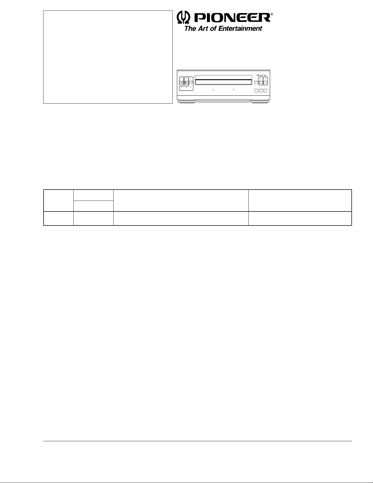
STEREO CASSETTE DECK
CT-R5
THIS MANUAL IS APPLICABLE TO THE FOLLOWING MODEL(S) AND TYPE(S).
Type
ZY ‡ DC power supplied from other system component
÷ These products are component of systems.
÷ This product does not operate normally by itself. Please connect it to the STEREO TUNER
AMPLIFIER SX-R9/MY, for adjustment and operation inspection. Otherwise damage may result.
Model
CT-R5
Power Requirement
Remarks
CONTENTS
1. SAFETY INFORMATION....................................2
2. EXPLODED VIEWS AND PARTS LIST .............3
3. SCHEMATIC DIAGRAM................................... 11
4. PCB CONNECTION DIAGRAM .......................16
5. PCB PARTS LIST.............................................24
6. ADJUSTMENT.................................................. 26
PIONEER ELECTRONIC CORPORATION 4-1, Meguro 1-Chome, Meguro-ku, Tokyo 153-8654, Japan
PIONEER ELECTRONICS SERVICE, INC. P.O. Box 1760, Long Beach, CA 90801-1760, U.S.A.
PIONEER ELECTRONIC (EUROPE) N.V . Haven 1087, Keetberglaan 1, 9120 Melsele, Belgium
PIONEER ELECTRONICS ASIACENTRE PTE. LTD. 501 Orchard Road, #10-00 Lane Crawford Place, Singapore 0923
CC
C PIONEER ELECTRONIC CORPORATION 1998
CC
7. GENERAL INFORMATION .............................. 30
7.1 IC................................................................ 30
7.2 BLOCK DIAGRAM .................................... 31
8. PANEL FACILITIES AND SPECIFICATIONS
...................................................................32
T–ZZR APR. 1998 Printed in Japan
Page 2
CT-R5
1. SAFETY INFORMATION
This service manual is intended for qualified service technicians; it is not meant for the casual
do-it-yourselfer. Qualified technicians have the necessary test equipment and tools, and have been
trained to properly and safely repair complex products such as those covered by this manual.
Improperly performed repairs can adversely affect the safety and reliability of the product and may
void the warranty. If you are not qualified to perform the repair of this product properly and safely, you
should not risk trying to do so and refer the repair to a qualified service technician.
WARNING
Lead in solder used in this product is listed by the California Health and Welfare agency as a known reproductive toxicant which
may cause birth defects or other reproductive harm (California Health & Safety Code, Section 25249.5).
When servicing or handling circuit boards and other components which contain lead in solder, avoid unprotected skin contact with
the solder. Also, when soldering do not inhale any smoke or fumes produced.
NOTICE
(FOR CANADIAN MODEL ONLY)
Fuse symbols (fast operating fuse) and/or (slow operating fuse) on PCB indicate that replacement parts
must be of identical designation.
REMARQUE
(POUR MODÈLE CANADIEN SEULEMENT)
Les symboles de fusible (fusible de type rapide) et/ou (fusible de type lent) sur CCI indiquent que les
pièces de remplacement doivent avoir la même désignation.
(FOR USA MODEL ONLY)
1. SAFETY PRECAUTIONS
The following check should be performed for the
continued protection of the customer and service
technician.
LEAKAGE CURRENT CHECK
Measure leakage current to a known earth ground
(water pipe, conduit, etc.) by connecting a leakage
current tester such as Simpson Model 229-2 or
equivalent between the earth ground and all exposed
metal parts of the appliance (input/output terminals,
screwheads, metal overlays, control shaft, etc.). Plug
the AC line cord of the appliance directly into a 120V
AC 60 Hz outlet and turn the AC power switch on. Any
current measured must not exceed 0.5 mA.
Reading should
not be above
0.5 mA
Earth ground
Device
under
test
Also test with plug
reversed
(Using AC adapter
plug as required)
Leakage
current
tester
Test all exposed
metal surfaces
AC Leakage Test
ANY MEASUREMENTS NOT WITHIN THE LIMITS
OUTLINED ABOVE ARE INDICATIVE OF A POTENTIAL SHOCK HAZARD AND MUST BE CORRECTED BEFORE RETURNING THE APPLIANCE
TO THE CUSTOMER.
2. PRODUCT SAFETY NOTICE
Many electrical and mechanical parts in the appliance have special safety related characteristics. These
are often not evident from visual inspection nor the
protection afforded by them necessarily can be obtained by using replacement components rated for
voltage, wattage , etc. Replacement parts which have
these special safety characteristics are identified in
this Service Manual.
Electrical components having such features are
identified by marking with a
on the parts list in this Service Manual.
The use of a substitute replacement component which
does not have the same safety characteristics as the
PIONEER recommended replacement one, shown in
the parts list in this Service Manual, may create shock,
fire, or other hazards.
Product Safety is continuously under review and
new instructions are issued from time to time. For
the latest information, always consult the current
PIONEER Service Manual. A subscription to, or additional copies of, PIONEER Service Manual may be
obtained at a nominal charge from PIONEER.
on the schematics and
2
Page 3
2. EXPLODED VIEWS AND PARTS LIST
NOTES : ÷ Parts marked by “ NSP ” are generally unavailable because they are not in our Master Spare Parts List.
÷ The
÷ Screw adjacent to ∞ mark on the product are used for disassembly.
2.1 PACKING
mark found on some component parts indicates the importance of the safety factor of the part.
Therefore, when replacing, be sure to use parts of identical designation.
PACKING PARTS LIST
CT-R5
6
5
4
7
Mark No. Description Part No.
1 Pad F AHA7199
2 Pad R AHA7200
3 Packing Case AHD7612
4 Operating Instructions ARE7178
( English/French/German/Italian/
Dutch/Spanish )
NSP 5 Warranty Card ARY7008
6 Caution Sheet ARM7034
7 Mirror Mat Sheet DHL1050
2
1
3
3
Page 4
CT-R5
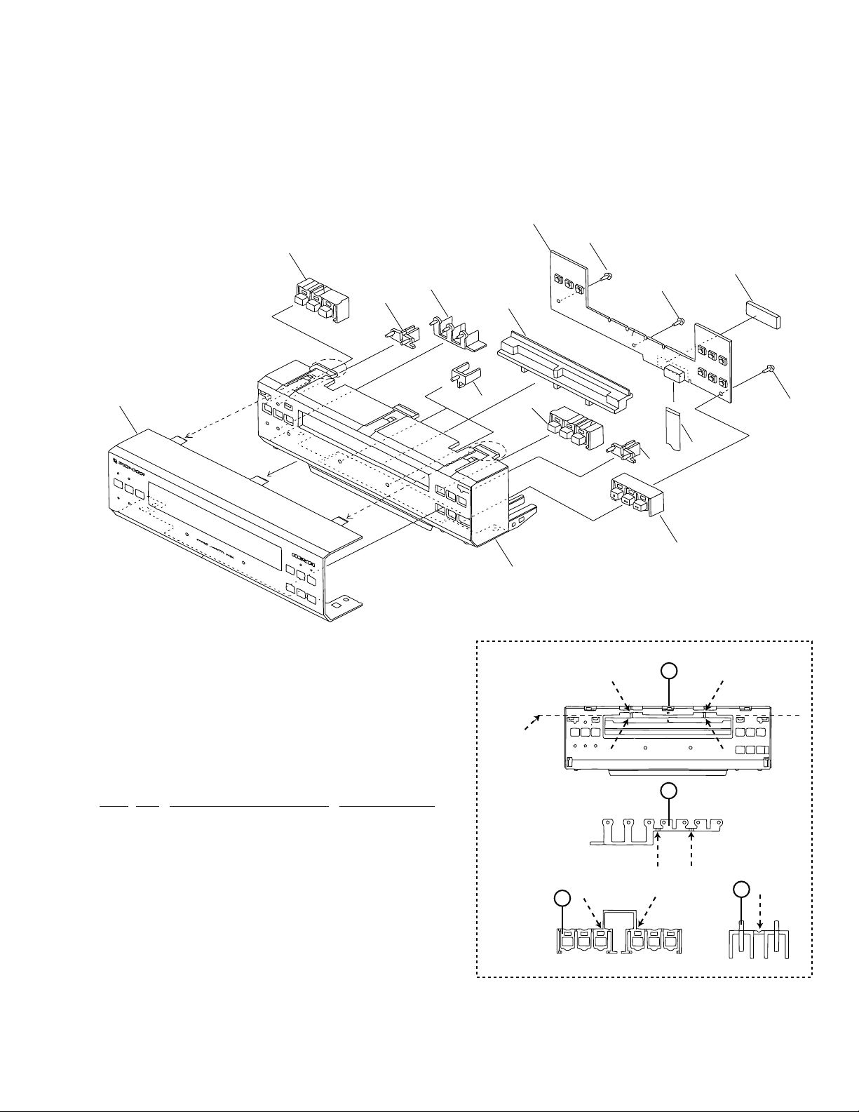
2.2 EXTERIOR
13
12
14
15
15
15
15
19
15
Refer to "2.4 MECHANISM
8
UNIT (1/2) "
11
15
16
7
18
6
15
9
15
15
15
4
17
Refer to "2.3 FRONT PANEL ".
17
÷ EXTERIOR SECTION PARTS LIST
Mark No. Description Part No.
NSP 1 Chassis ANA7063
2 Foot AEC7114
3 Insulator Assy AMR7189
NSP 4 PCB Mold AMR2115
5 Rear Panel ANC7686
5
2
1
3
15
10
15
15
Mark No. Description Part No.
11 Bonnet AZN7701
12 Tray Panel AAK7469
13 Tray Cap AAK7471
NSP 14 Tray Seal RRW1162
15 Screw VBZ30P080FZK
6 CONNECT ASSY AWZ8894
7 Connection Cable ADE7018
8 Mechanism Unit RYM1264
9 MAIN ASSY AWZ8891
10 MCON ASSY AWZ8893
4
16 Screw BBZ30P140FMC
17 Screw BBT30P080FZK
18 Cord Clamper RNH-184
19 Screw BBZ30P100FMC
Page 5
1
2
4
9
6(3/3)
3(2/2)
11
10
11
11
8
7
5
6(2/3)
6(1/3)
3(1/2)
2.3 FRONT PANEL
Cut
Cut
Cut
Cut
Cut
Cut
Cut
Cut
Cut
6
2
5
3
Cut limit line
not be ferced
out !
Part cut
CT-R5
÷ FRONT PANEL SECTION PARTS LIST
Mark No. Description Part No.
1 Front Panel ANB7106
2 Panel Base AMB7461
3 Play Button AAD7413
4 FF Button AAD7414
5 LED Lens A AAK7472
6 LED Lens B AAK7473
7 Blind Mould AZA7263
8 FRONT ASSY AWZ8892
9 Lead Card 12P ADD7073
10 Poron Seat AEB7095
11 Screw PPZ30P080FMC
5
Page 6
CT-R5
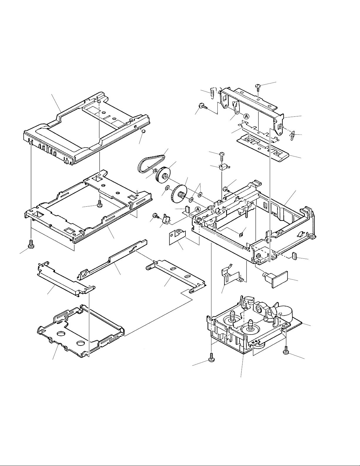
2.4 MECHANISM UNIT (1/2)
19
10
11
9
2
7
1
3
13
1
27
21
29
3
25
30
26
6
7
28
30
8
22
24
16
4
18
17
15
12
23
20
28
31
32
14
5
Refer to "2.5 MECHANISM UNIT (2/2)".
5
6
Page 7

MECHANISM UNIT (1/2) PARTS LIST
Mark No. Description Part No.
1 Screw BBZ26P050FZK
2 Bearing 5φ PBP-007
3 Screw PBZ20P080FMC
4 Screw PMZ20P040FZK
5 Screw PPZ30P060FMC
6 Washer WA21D040D050
7 Washer WT16D040D050
8 Plate RNE1937
9 Screw (M1.7 X 8.2-7) RBA1124
10 Screw (M1.4 X 2BK) RBA1125
11 Spring A RBH1451
12 Spring B RBH1452
13 Chassis 576 RNE1915
14 Holder Assy RNE1916
15 Arm-576 RNE1917
16 Retainer RNE1918
17 Plate Earth RNE1919
18 Nut RNE1920
19 Tray-578 RNK2265
20 Flame Assy RNK2266
CT-R5
21 Arm A RNK2267
22 Arm C RNK2268
23 Plate RNK2269
24 Arm RNK2270
25 Pulley C RNK2285
26 Gear-B RNK2286
27 Gear Luck RNK2273
28 Buffer RNK2274
29 Belt-49.2 REB1312
30 Switch MSS-8B RSG1045
31 Motor PCB Assy RXM1089
32 C. Deck ADR2178TB RYM1260
7
Page 8
CT-R5
2.5 MECHANISM UNIT (2/2
1
45
1
36
19
27
6
11
2
5
49
)
34
19
35
10
51
38
15
51
2
12
49
7
16
46
18
33
17
1
42
48
40
44
14
17
8
24
25
9
26
32
47
30
23
52
1
26
32
32
31
3
13
41
48
20
37
4
14
4
1
14
4
22
21
1
20
29
28
39
50
43
8
Page 9

CT-R5
÷ MECHANISM UNIT
(
2/2) PARTS LIST
Mark No. Description Part No.
1 Screw BCZ20P040FMC
2 Cap Reel RNK2284
3 Screw S RBA1122
4 Screw M RBA1123
5 Spring-B/T R RBH1443
6 Spring-Lever AC RBH1444
7 Spring-Base Head RBH1445
8 Spring-Cam Lock RBH1446
9 Spring-Arm RF RBH1447
10 SPR-Pinch Return F RBH1448
11 SPR-Pinch Return R RBH1449
12 Spring-B/T F RBH1450
13 Hall IC REA1262
14 Cushion Motor REB1311
15 Plate-Spring RNE1910
16 Plate Shield RNE1911
17 BRKT Side RNE1912
18 BRKT M/T Top RNE1913
19 Bush Reel RNK2283
20 Base-Reel RNK2253
21 Gear-Cam RNK2254
22 Gear-Idler RNK2255
23 Lever-Brake RNK2256
24 Arm-Cam Lock RNK2257
25 Arm-RF RNK2258
Mark No. Description Part No.
46 DC Motor Assy RXM1088
47 Connector S13B–PH–K–S
48 Washer WA26D045D025
49 Washer WA62D095D025
50 Washer WT10D035D025
51 Washer WT15D040D050
52 Plate Loader RNE1939
26 Gear-RF RNK2259
27 Lever-AC RNK2260
28 Cap-Magnet RNK2261
29 Plate Magnet RNK2262
30 PCB Control 2103 RNP1707
31 Switch Mode RSG1044
32 Switch Detect RSN1026
33 Chassis (OS) Assy RXA1756
34 Chassis (HEAD) Assy RXA1757
35 Pinch Roller Assy (F) RXA1758
36 Pinch Roller Assy (R) RXA1759
37 Flywheel (R) Assy RXA1760
38 Arm (PLAY) Assy RXA1761
39 Clutch Fast Assy RXA1763
40 Flywheel (F) Assy RXA1764
41 Clutch Play Assy RXA1765
42 Solenoid RXP1022
43 Belt Sub REB1308
44 Belt Main REB1309
45 R/P Head Assy RXA1766
9
Page 10

CT-R5
10
Page 11

1
23
4
CT-R5
3. SCHEMATIC DIAGRAM
Note: When ordering service parts, be sure to refer to "EXPLODED VIEWS AND PARTS LIST" or "PCB PARTS LIST".
3.1 OVERALL SCHEMATIC DIAGRAM
MAIN ASSY
A
(AWZ8891)
MECHANISM UNIT
(RYM1264)
CN201
B4B–PH–K–S
CN202
B3B–PH–K–S
A
To TUNER AMPLIFIER
SX-R9 CN103
B
CN106
B6B–PH–K–S
MCON ASSY
C
(AWZ8893)
CONNECT ASSY
B
(AWZ8894)
FRONT ASSY
D
(AWZ8892)
To MD RECORDER
MJ-R5 CN101
C
D
CN403
B13B–PH–K–S
11
1
2
3
4
Page 12

1
CT-R5
3.2 MAIN ASSY
A
MECHANISM
UNIT (1/2)
(RYM1264)
REC/PB
HEAD
RXA1766
MAIN ASSY (AWZ8891)
A
234
PB AMP
DOLBY–B NR
–5V
PB LEVEL L
ERASE
HEAD
B
REC AMP
Film
Ceramic
Ceramic
Ceramic
Unmarked
*
C
: 1SS 254
PB LEVEL R
5V
REC MUTE
REC LEVEL L
REC LEVEL R
BIAS OSC.
BIAS LEVEL R
D
12
A
1234
BIAS LEVEL L
Page 13

5
67
8
CT-R5
: PLAYBACK SIGNAL
: RECORDING SIGNAL
PB MUTE
MS
ALC
A
B
MPX FILTER
C
CN105
B
6.4V
–6.4V
D
5
6
7
8
A
13
Page 14

1
234
CT-R5
3.3 CONNECT ASSY, MCON ASSY AND FRONT ASSY
C
A
MECHANISM
UNIT (2/2)
(RYM1264)
MECHA DRIVER
B
MCON ASSY (AWZ8893)
TEST MODE
LOADING
MOTOR
C
CN401
To TUNER AMPLIFIER
SX-R9 CN103
C
7V
CN402
–7V
C
D
14
B C
1234
To MD RECORDER MJ-R5 CN101
Page 15

5
67
8
CT-R5
B
CN103
B
CN104
FRONT ASSY (AWZ8892)
D
SWITCHES:
S511: STOP
S512: REW
S513: FF
S514: FWD
S515: REV
S516: OPEN/CLOSE
S517: REC
S518: DOLBY NR
S519: REVERSE
MODE
A
B
Q451–Q458: DTC143EK
C
:
5V
–5V
CONNECT ASSY
B
(AWZ8894)
CN203
A
: PLAYBACK SIGNAL
: RECORDING SIGNAL
D
CAUTION: FOR CONTINUED PROTECTION
AGAINST RISK OF FIRE.
NO. AEK7009, MFD BY LITTEL
FUSE INK.FOR IC101 AND IC102.
5
6
B C
7
D
8
15
Page 16

1
234
CT-R5
4. PCB CONNECTION DIAGRAM
4.1 MAIN ASSY , CONNECT ASSY
A
NOTE FOR PCB DIAGRAMS:
1. Part numbers in PCB diagrams match those in the schematic
diagrams.
2. A comparison between the main parts of PCB and schematic
diagrams is shown below.
Symbol in PCB
Diagrams
BCE
BCE
Symbol in Schematic
Diagrams
BCE
BCEBCE
BCE
Part Name
Transistor
Transistor
with resistor
A
MAIN ASSY
B
DGS
3. The parts mounted on this PCB include all necessary parts
for several destination.
For further information for respective destinations, be sure
to check with the schematic diagram.
4. Viewpoint of PCB diagrams
C
P. C. Board Chip Part
DGSDGS
CapacitorConnector
ANP7205–B
Field effect
transistor
Resistor array
3-terminal
regulator
SIDE A
SIDE B
Q331
Q334Q333Q332
To MECHANISM UNIT (1/2)
ERASE HEAD
To MECHANISM UNIT (1/2)
REC/PB HEAD
B
VR332VR331
Q335
Q102
CONNECT ASSY
Q201
Q202
D
Q112 IC111
Q111
16
A B
Q101Q102
1234
Page 17

5
67
8
CT-R5
SIDE A
A
B
VR201 VR202 VR301 VR302
To MD RECORDER
MJ-R5 CN101
IC231 Q336 Q306 Q305
Q253
To MECHANISM UNIT (2/2)
C
C
CN402
IC102
IC101
To TUNER AMPLIFIER
SX-R9 CN103
5
C
CN401
D
A B
6
7
8
17
Page 18

A
B
CT-R5
1
A
234
MAIN ASSY
Q251 Q252
C
IC251 Q353
B
CONNECT ASSY
Q352 Q232
Q351
Q231
D
ANP7205–B
18
A
B
1234
Page 19

5
67
8
CT-R5
SIDE B
A
B
Q205
Q206
IC201
IC301Q301–Q304
Q203
Q204
IC207
SIDE B
C
D
A
5
6
7
B
8
19
Page 20

1
CT-R5
4.2 MCON ASSY, FRONT ASSY
A
B
234
D
FRONT ASSY
C
MCON ASSY
C
Q410
Q408
B
CN104
D
B
CN103
Q409
Q407 Q401
20
C
D
1234
Page 21

5
67
8
CT-R5
SIDE A
A
B
To MECHANISM UNIT (2/2)
Q402 Q405 Q403
C
D
5
6
7
C
D
8
21
Page 22

A
B
CT-R5
1
234
D
FRONT ASSY
C
MCON ASSY
C
Q451–Q458 Q404 Q406 IC401
D
22
C
D
1234
Page 23

5
67
8
CT-R5
A
SIDE B
B
SIDE B
C
ANP7205–B
D
5
6
7
C
D
8
23
Page 24

CT-R5
5. PCB PARTS LIST
NOTES : ÷ Parts marked by “ NSP ” are generally unavailable because they are not in our Master Spare Parts List.
÷ The
÷ When ordering resistors, first convert resistance values into code form as shown in the following examples.
mark found on some component parts indicates the importance of the safety factor of the part.
Therefore, when replacing, be sure to use parts of identical designation.
Ex. 1 When there are 2 effective digits (any digit apart from 0), such as 560 ohm and 47k ohm (tolerance is shown by
J = 5%, and K = 10%).
1
560 Ω = 56 × 10
47k Ω = 47 × 10
= 561................................................... RD1/4PU 5 6 1 J
3
= 473 .................................................. RD1/4PU 4 7 3 J
0.5 Ω = R50 ...................................................................... RN2H Â 5 0 K
1 Ω = 1R0 ......................................................................... RS1P 1 Â 0 K
Ex. 2 When there are 3 effective digits (such as in high precision metal film resistors).
5.62k Ω = 562 × 10 1 = 5621 ........................................... RN1/4PC 5 6 2 1 F
Mark No. Description Part No.
LIST OF PCB ASSEMBLIES
NSP TC MAIN ASSY AWM7302
A
SEMICONDUCTORS
COILS AND FILTERS
CAPACITORS
MAIN ASSY AWZ8891
FRONT ASSY AWZ8892
MCON ASSY AWZ8893
CONNECT ASSY AWZ8894
MAIN ASSY
IC201,IC251,IC301 BA4558F-HT
IC231 CXA1101P
Q334 2SB1238X
Q331,Q332 2SC1815
Q353 2SC2412K
Q251,Q252,Q303,Q304 2SD2114K
Q351,Q352 2SD2114K
Q333 2SD2144S
Q201,Q202 2SK373
Q207, Q231,Q232 DTA124EK
Q306, Q336 DTA124ES
Q253, Q305 DTA143ES
Q203- Q206, Q301, Q302 DTC114TK
Q335 DTC124ES
D201- D206, D251–D253 1SS254
D351- D353 1SS254
L331 (OSC. COIL) ATX7002
L301, L302 (10 mH) RTF1004
L303, L304 (3.3 mH) RTF1019
F351, F352 (MPX. FILTER) RTF1217
C201, C202 CCSQCH100D50
C901, C902 CCSQCH101J50
C233, C253 CCSQCH121J50
C203, C204 CCSQSL471J50
C235, C236 CEASR68M50
C233,C234,C340 CEAT100M50
C237,C238 CEAT101M10
C355 CEAT220M50
Mark No. Description Part No.
C231,C232,C251,C252 CEAT2R2M50
C303, C304, C351- C318 CEAT2R2M50
C309, C310 CEAT330M16
C205, C206 CEAT330M25
C209, C210, C319,C320 CEAT470M16
C334, C335 CEAT470M16
C353, C354 CFTYA103J50
C336 CFTYA223J50
C903,C904 CKSQYB152K50
C301, C302 CKSQYB221K50
C307,C308 CKSQYB272K50
C338,C339 CKSQYB332K50
C311,C312 CKSQYB333K25
C313,C314 CKSQYB393K50
C337 CKSQYB472K50
C207,C208 CKSQYB682K50
C305,C306 CKSQYB823K25
C254 CKSQYF105Z16
C333 CQHA822J2A
RESISTORS
R336 RD1/2VM111J
R338 RD1/2VM161J
R335 RD1/2VM4R7J
R262 RD1/4PU101J
R359, R360 RD1/4PU102J
R232- R235, R319, R320 RD1/4PU103J
R255 RD1/4PU222J
R231 RD1/4PU433J
R267, R325 RD1/4PU473J
R263 RD1/4PU751J
R215, R216, R323,R324 RD1/4PU820J
VR201, VR202 (4.7 kΩ) PCP1028
VR301, VR302 (4.7 kΩ) RCP1139
VR331, VR332 (220 kΩ) RCP1142
Other Resistors RS1/10S&&&J
OTHERS
CN202 KR CONNECTOR(3P) B3B-PH-K-S
CN201 KR CONNECTOR B4B-PH-K-S
CN203 2mm CONNECTOR TUC-P17X-B1
PCB BINDER VEF1040
24
Page 25

CT-R5
Mark No. Description Part No.
B
CONNECT ASSY
SEMICONDUCTORS
IC101,IC102 (Protector 1A) AEK7009
IC111 BU4066BC
Q102 2SB1237X
Q101 2SD1858X
Q111 DTA143ES
Q112 DTC143ES
D105,D111 1SS254
D101,D102 MTZJ5.6B
D103,D104 S5688G
CAPACITORS
C113, C114 CEAT2R2M50
C101,C102 CEAT470M16
C111,C112 CKSQYB103K50
C103,C104 CKSQYF104Z50
RESISTORS
R105,R106 RS1/10S103J
Other Resistors RD1/4PU&&&J
OTHERS
CN101 19P CONNECTOR AKP7002
CN102 19P SOCKET AKP7013
CN106 KR CONNECTOR B6B-PH-K-S
CN103 2mm CONNECTOR TUC-P10P-B1
CN104 2mm CONNECTOR TUC-P11P-B1
Mark No. Description Part No.
RESISTORS
All Resistors RD1/4PU&&&J
OTHERS
CN404 12P FFC CONNECTOR 9607S-12F
CN403 KR CONNECTOR B13B-PH-K-S
CN401 2mm CONNECTOR TUC-P10X-B1
CN402 2mm CONNECTOR TUC-P11X-B1
X401 CERAMIC RESONATOR VSS1045
FRONT ASSY
D
PCB BINDER VEF1040
( 6.00 MHz )
SEMICONDUCTORS
D501 - D509 LED(RED) SLR-342VCT31
SWITCHES AND RELAYS
S511 - S519 ASG1034
RESISTORS
R504 RD1/4PU181J
R501 -R503,R505,R506 RD1/4PU331J
Other Resistors RS1/10S&&&J
OTHERS
CN501 12P FFC CONNECTOR 9607S-12F
PCB BINDER VEF1040
CN105 2mm CONNECTOR TUC-P17P-B1
KN101 EARTH METAL FITTING VNF1084
C
MCON ASSY
PCB BINDER VEF1040
SEMICONDUCTORS
IC401 PDC044A
Q403,Q405 2SA1560
Q407,Q408 2SB1859X
Q407,Q410 2SD1859X
Q402 DTA124ES
Q401 DTC124ES
Q404,Q406,Q451- Q458 DTC143EK
D402,D403 1SS254
CAPACITORS
C401 CEAT471M6R3
C402,C405,C406 CKSQYB103K50
C404,C407,C408 CKSQYB471K50
C403 CKSQYF105Z16
25
Page 26

CT-R5
6. ADJUSTMENT
When the adjustment is made, the product should be connected to a STEREO TUNER AMPLIFIER (SX-R9) .
For your information, another method (without using the tuner amp.) is explained here.
6.1 TEST MODE
7 How to enter the Test Mode
* In case that the product is connected to an SX-R9
Select either of the following procedures:
1. By using the remote control, turn on the power to the
CT-R5 and receive the " A15F " signal from the
tuner amp through the bus.
2. With Power OFF, connect the Pin-15 of the micro computer to GND, and short the TEST MODE
jumper wires W159(TEST) and W160(GNDD) each
other on the MCON ASSY. Then turn on the power
by using the remote control. (Refer to Fig. 6-1.)
TEST MODE
W159
W160
Short point
MCON ASSY
A
CONNECT ASSY
14
12
6
+7.0V
–7.0V
Fig.6-2
7 Test mode operations
- When the product enters the test mode, two center LEDs will
flash .
- All operation buttons, except for the [REC] and [REVERSE
MODE] Buttons, provide normal operations in the mode.
- When all LEDs remain extinguished, shift the TC/MD signal
selector to the MD side inside the CT-R5.
(1) LED check
Each time the [REVERSE MODE] button is pushed, the LED
operation changes as follows:
Normal display = All LEDs ON = All LEDs OFF = Leaf
+ SW check
(2) Leaf SW check
When the leaf switches are depressed, their corresponding
LEDs light up as follows:
+5.6V
Fig . 6 - 1
* In case that an SX-R9 is not available for adjustment
- On the CONNECT ASSY, short the pin -7 (GNDD:W128),
pin -13 (GNDR:W127) and pin-17 (GNDA:W126) of
CN101 one another. (Refer to A)
- On the MCON ASSY, short the TEST MODE jumper
wires W159(TEST) and W160(GNDD) each other.
(Refer to Fig. 6-1.)
- Apply the DC power voltage to the Pin-6(+5.6V), Pin-12
(-7V), and Pin-14(+7V) of respectively.
(Refer to Fig. 6-2.)
26
Leaf switch LED
REV REC SW .............................. REC LED
FEW REC SW .............................. FWD LED
CrO
2 SW ........................................ DOLBY LED
HALF SW ...................................... REV LED
(3) Auto REC/PLAY operation mode
Push the [REC] button. The auto REC/PLAY operation mode
starts:
1. Sets the function of tuner amp to AUX.
2. One second later, starts 5-second FWD recording.
3. Performs REV recording for 5 seconds.
4. Shifts the function to TAPE, then performs FWD play for
5 seconds.
5. Stops operations.
* When the [REC] button is pushed once again, the above
operations are repeated.
** After the auto REC/PLAY operation is completed, when the
[REV] button is pushed, CT-R5 performs REV play for 5
seconds and stops operations.
7 How to cancel the test mode
To cancel the test mode, push the “POWER” button on the the
tuner amp to turn off the power to the CT-R5.
Page 27

6.2 ADJUSTMENT
7 Adjustment Condition
(1) The ground at the time of adjustment shall be W153.
(Refer to Fig. 6–5).
(2) Clean the heads and demagnetize them using a head eraser.
(3) Set the measurement level to 0 dBV = 1 Vrms.
(4) Use the specified tape for adjustment. Use the labeled (A) side
of the test tape.
NCT–111 : For Tape Speed adjustment
NCT-132X : For Playback adjustment
STD–632 : Normal blank tape
* As the reference recording level is 250 nwb/m for NCT–
132X, the recording level will be higher by 4 dB for STD–
331B (160nwb/m). When adjusting, pay carefull attention
to the type of tape used.
(5) Provide yourself with the following measuring devides:
÷ AC millivoltmeter
÷ Low-frequency oscillator
÷ Attenuator
÷ Oscilloscope
(6) Adjust both right and left channels unless otherwise specified.
(7) Turn the DOLBY NR switch off unless otherwize specified.
(8) Warm up the unit for several minutes before adjustment. In
particular, be sure to warm up the unit in the REC/PLAY mode
for 3 to 5 minutes before starting recording/playback frequency
characteristics adjustment.
(9) Always follow the indicated adjustment order.
Otherwise, a complete adjustment may not be achieved.
7 List of Adjustments
¶ Playback Section
(1) Tape Speed Confirmation
(2) Head Azimuth Adjustment
(3) Playback Level Adjustment
¶ Recording Section
(1) Recording Bias Adjustment
(2) Recording Level Adjustment
PLAY BACK
250
3dB
RECORDING
250
3dB
10k
10k
3dB
3dB
CT-R5
12.5k
4dB
315Hz=0dB
12.5k
5dB
Note: In case of adjustment as a single unit, connect a 22 kΩ load
resistor to pins 16(PBR) and 18 (PBL)of CN101(CONNECT
ASSY).
0 dB
30s
315 Hz
0 dB: 315 Hz, 250 nwb/m
30 s 30 s 30 s 10s 10s .......................................................................................................... 10s
6.3 kHz 10 kHz 315 Hz 14 kHz
Fig. 6–4 Test Tape NCT-132X
12.5
kHz
315Hz=0dB
Fig. 6–3 Frequency Characteristics
Dolby noise reduction manufactured under license from Dolby
Laboratories Licensing Corporation.
“DOLBY” and the double-D symbol are trademarks of Dolby
Laboratories Licensing Corporation.
10 kHz
8 kHz 4 kHz 2 kHz
6.3
kHz
1 kHz
500Hz250Hz125
Hz
63 Hz 40 Hz
–20 dB
27
Page 28

CT-R5
6.2.1 Playback Section
(1) Tape Speed Confirmation
No. Mode Input Signal/Test Tape Adjustment Points Measurement Points Adjustment Value Remarks
PLAY1
NCT-111 (3 kHz)
VR (Mechanism Unit)
(Refer to Fig. 6–5)
TP R (W162)
( MAIN ASSY)
(2) Head Azimuth Adjustment
¶ This unit is equipped with auto tape selector.
¶ Do not switch between forward and reverse operation with the screwdriver inserted.
No. Mode Input Signal/Test Tape Adjustment Points
PLAY1
NCT–132X test tape
(Playback: 10 kHz, –20 dB)
Head azimuth
adjustment Screw
(Fig. 6–5)
Measurement
Points
TP L (W161)
TP R (W162)
( MAIN ASSY)
(3) Playback Level Adjustment
¶ Since this adjustment determines playback DolbyNR level, Perform it carefully.
Measurement
Points
1
PLAY
NCT-132X test tape
(Playback: 315 Hz, 0 dB)
L ch
R ch VR202
VR201
TP L (W161)
TP R (W162)
( MAIN ASSY)
3000 Hz Hz
Adjustment
Value
Max. Playback
signal level
Adjustment
Value
–4.2 dBV
+90
–60
Adjustment only when
outside the standard
Remarks
After adjustment, apply silicon
bond to the head azimuth
adjustment screw.
RemarksNo. Mode Input Signal/Test Tape Adjustment Points
6.2.2 Recording Section
(1) Recording Bias Adjustment
¶ After the adjustment, caution should be exercised so as not to become under bias by checking the distortion rate.
No. Mode Input Signal/Test Tape Adjustment Points
REC/
1
PAUSE
REC =
2
PLAY
Input a 315Hz signal to the AUX
terminal of SX-R9. ∗
Load the STD–632 test tape and
record/playback the 315Hz and
10kHz signals. (see the Note below)
Input signal level –24.2 dBV
L ch
R ch VR332
VR331
Measurement
Points
TP L (W161)
TP R (W162)
( MAIN ASSY)
Note: Set the 10kHz input signal level to the same value as the 315Hz input signal level of step 1.
(2) Recording Level Adjustment
No. Mode Input Signal/Test Tape Adjustment Points
REC/
1
PAUSE
REC =
2
PLAY
Input a 315Hz signal to the AUX
terminal of SX-R9. ∗
STD–632 test tape and record/
playback the 315Hz signal.
Input signal level –8.2 dBV
L ch
R ch VR302
VR301
Measurement
Points
TP L (W161)
TP R (W162)
( MAIN ASSY)
Adjustment
Value
Repeat adjustment until playback level of
the 10kHz signal is within 0 ±0.5dB from
that of the 315Hz signal.
Adjustment
Value
Repeat recording, playback and
adjustment until playback level of the
315Hz signal becomes –
Remarks
Remarks
8.2dBV±0.5dB
.
*: In case of adjustment as a single unit, enter the signal at 15P(RECR) and 19P(RECL) of CN101(CONNECT ASSY). At this time, connect
an output buffer amplifier to the oscillator, and then connect a series resistor (180 Ω) after the impedance has become sufficiently low. (For
MPX filter impedance matching)
28
Page 29

CT-R5
PB LEVEL
REC LEVEL
MAIN ASSY
VR332
(R ch)
VR331
(L ch)
REV Azimuth
Adjustment Screw
Tape speed adjustment VR
NOTE: Always use a ceramic
screwdriver for adjustment.
FWD Azimuth
Adjustment Screw
BIAS LEVEL
Front
VR201
(L ch)
VR202
(R ch)
VR302
(R ch)
VR301
(L ch)
Mesurement
Points
TAPE TEST POINT
W161 (L ch)
W153 (GND)
W162 (R ch)
MECHANISM UNIT
Front
Fig. 6–5 Adjustment and Measurement Points
29
Page 30

CT-R5
7. GENERAL INFORMATION
7.1 IC
7 PDC044A (IC401: MCON ASSY )
¶ System Micro-computer
¶ Pin Function
No. Name I/O Description
1 TC/XMD O Switching Signal H :TC / L : MD
2 XT OUT O L: Loading mechanism OPEN (Nch O.D.)
3 XT IN O L: Loading mechanism CLOSE(Nch O.D.)
4 S. CLK I System bus CLOCK
5 XRESET I Reset
6 NC –– Connected to VDD
7 NC –– Not used
8 NC –– Connected to VDD
9 VSS –– Power supply (–) terminal VSS
10 CF1 I
Connected to Ceramic oscillator
11 CF2 O ( 6 MHz)
¶ The information shown in the list is basic information and may not
correspond exactly to that shown in the schematic diagrams.
No. Name I/O Description
27 LED 8 O H: FWD
28 LED 7 O H: REV
29 NC –– Not used
30 LED 6 O H: POWER ON
31 LED 5 O H: DOLBY
32 LED 4 O H: REC
33 LED 3 O H: REPEAT
34 LED 2 O H: A → B
35 LED 1 O H: ONEWAY
36 SO O System bus Data OUTPUT
37 SI I System bus Data INPUT
12 VDD –– Power supply (+) terminal
13 KEY1 I key data input (A/D)
14 KEY2 I key data input (A/D)
15 XTEST I TEST MODE detection L: TEST IN
16 MS I Audio signal detection for MS H: MS
17 PULSE I Cassette mechanism Pulse input
18 NC –– Not used
19 XREC-F I FWD REC detection switch (L: ON ban)
20 XHALF I L: Tape detection switch ON
21 XREC-R I REV REC detection switch (L: ON ban)
22 XCr SW I L : CrO2 detection switch ON
23 XMODE I L: MODE detection switch ON
24 NC –– Not used
25 MOTOR O Cassette mechanism motor ON
26 SOL O Loading mechanism Solenoid ON
38 S.REQ I/O System bus Request
39 XOPEN I L: Tray open explicit switch ON
40 XCLOSE I L: Tray close explicit switch ON
41 BIAS O H: BIAS oscillation ON
42 NC –– Not used
43 XCrO2 O Switching tape type H:NORMAL / L:CrO2
44 XREC MUTE O L: REC MUTE ON
45 XPB/REC O Switching L: PB / H: REC
46 XDOLON O L: DOLBY NR ON
47 XPBMUTE O L: PB MUTE ON
48 NC –– Not used
30
Page 31

7.2 BLOCK DIAGRAM
TO SX-R9
CT-R5
FROM MJ-R5
PB
IC111
BU4066BC
PLAYBACK SIGNAL
RECORDING SIGNAL
:
:
TC
MAIN ASSY
PB MUTE
REC
TC/MD SELECT
MD
Q112
Q111
1
PB
TC/XMD
IC401
PDC044A
TC µ-COM
REC
CONNECT ASSY
LED
V+6
LED1-8
KEY
KEY1-2
11
IC231
CXA1101P
DOLBY-B NR
CT-R5 BLOCKDIAGRAM
IC201
14
5
16
39
7
1
IC301
PB EQ AMP
M
DECK
MECHA
RYM1264
BIAS
OSC
REC EQ AMP
25
MOTOR
MOTOR
DRIVER
A/D
MCON ASSY
FRONT ASSY
31
Page 32

CT-R5
8. PANEL FACILITIES AND SPECIFICATIONS
7 PANEL FACILITIES
2
1
D
REC DOLBY
¶
O
p ∏
3
4
REVERSE
MODE
NR
AUTO REVERSE/FRONT LOADING MECHANISM
STEREO CASSETTE DECK
-
1 DOLBY * B NR (Dolby B-type NR ON/OFF ) button
/ indicator
2 Recording pause button (¶ 8) / indicator
3 Reverse mode button / indicator
4 Cassette tray
5 Rewind button (1)
6 Fast forward button (¡)
7 Stop button (7)
0
8
9
OPEN
/CLOSE
REV FWD
23
0
REW FFSTOP
1¡
7
7
5
8 Reverse Playback button (2) / indicator
9 Forward Playback button (3) / indicator
0 Cassette tray Open / Close button (0)
- POWER on / indicator
*
¶ Dolby noise reduction manufactured under license
from Dolby Laboratories Licensing Corporation.
¶ “DOLBY” and the double-D symbol are trademarks
of Dolby Laboratories Licensing Corporation.
6
7 SPECIFICATIONS
Tracking method ................................. 4-track, 2-channel stereo
Frequency response
Type I (Normal) tape........................ 20 Hz – 16,000 Hz ± 6 dB
Type II (High/CrO2) tape................... 20 Hz – 16,000 Hz ± 6 dB
Signal-to-Noise Ratio .......................................................... 55 dB
(EIAJ, peak recording level, audio compensation)
Dolby B NR ON .............................. 10 dB improvement at 5 kHz
Wow and Flutter ..................................................... 0.07% WRMS
External dimensions ................ 210 (W) x 75 (H) x 269.5 (D) mm
Weight .................................................................................... 2.0 kg
Accessories
Supplementary Operating Instructions ..................................... 1
Warranty Card .............................................................................. 1
Caution Sheet ............................................................................... 1
NOTE:
Specifications and design subject to possible modification without notice,
due to improvement.
(when recorded at –20 dB)
32
 Loading...