

Page 1
PLAY
23
!
¶8
REC PAUSE
EJECT
STOP07
RRV2471
STEREO CASSETTE DECK
CT-L11
THIS MANUAL IS APPLICABLE TO THE FOLLOWING MODEL(S) AND TYPE(S).
Type
MYXJ AC220-230V
NVXJ AC230V
¶ This product is a system(s) component.
This product does not function properly independently ; to avoid malfunctions, be
sure to connect it to the prescribed system component(s), otherwise damage may
result.
¶ Please connect it to the POWERED SUBWOOFER S-DV88SW or S-DV77SW, for
adjustment and operation inspection.
¶ Please connect it to the STEREO CD TUNER XC-L11 and the POWER STEREO
AMPLIFIER M-L11, for adjustment and operation inspection.
DVD/CD TUNER XV-DV88 XV-DV77 RRV2480
SPEAKER SYSTEM ––– S-DV77 RRV2473
SATELLITE SPEAKER S-DV88ST S-DV77ST RRV2486, RRV2473
POWERED SUBWOOFER S-DV88SW S-DV77SW RRV2474, RRV2473
STEREO CD TUNER XC-L11 RRV2470
STEREO POWER AMPLIFIER M-L11 RRV2479
MINIDISC RECORDER MJ-L11 RRV2472 System option
STEREO CASSETTE DECK CT-L11 RRV2471 This manual.
Model
CT-L11
Component Model Service manual Remarks
Power Requirement Remarks
ORDER NO.
CONTENTS
1. SAFETY INFORMATION
2. EXPLODED VIEWS AND PARTS LIST
3. BLOCK DIAGRAM AND SCHEMATIC DIAGRAM
4. PCB CONNECTION DIAGRAM
5. PCB PARTS LIST
6. ADJUSTMENT
PIONEER CORPORATION 4-1, Meguro 1-chome, Meguro-ku, Tokyo 153-8654, Japan
PIONEER ELECTRONICS SERVICE, INC. P.O. Box 1760, Long Beach, CA 90801-1760, U.S.A.
PIONEER ELECTRONIC NV Haven 1087, Keetberglaan 1, 9120 Melsele, Belgium
PIONEER ELECTRONICS ASIACENTRE PTE. LTD. 253 Alexandra Road, #04-01, Singapore 159936
c
PIONEER CORPORATION 2001
...............................................
....................................................
......................................
................
....
..........................
2
3
8
14
20
23
7. GENERAL INFORMATION
7.1 DIAGNOSIS
7.1.1 DISASSEMBLY
7.1.2 POWER ON SEQUENCE
7.2 PARTS
7.2.1 IC
8. PANEL FACILITIES AND SPECIFICATIONS
............................................................
.................................................
.........................................................
................................
......................................
......................
T–ZZR JUNE 2001 Printed in Japan
....
28
28
28
30
31
31
32
Page 2
CT-L11
1. SAFETY INFORMATION
This service manual is intended for qualified service technicians ; it is not meant for the casual do-ityourselfer. Qualified technicians have the necessary test equipment and tools, and have been trained
to properly and safely repair complex products such as those covered by this manual.
Improperly performed repairs can adversely affect the safety and reliability of the product and may
void the warranty. If you are not qualified to perform the repair of this product properly and safely, you
should not risk trying to do so and refer the repair to a qualified service technician.
WARNING
This product contains lead in solder and certain electrical parts contain chemicals which are known to the state of California to cause
cancer, birth defects or other reproductive harm.
Health & Safety Code Section 25249.6 – Proposition 65
NOTICE
(FOR CANADIAN MODEL ONLY)
Fuse symbols (fast operating fuse) and/or (slow operating fuse) on PCB indicate that replacement parts must
be of identical designation.
REMARQUE
(POUR MODÈLE CANADIEN SEULEMENT)
Les symboles de fusible (fusible de type rapide) et/ou (fusible de type lent) sur CCI indiquent que les pièces
de remplacement doivent avoir la même désignation.
(FOR USA MODEL ONLY)
1. SAFETY PRECAUTIONS
The following check should be performed for the
continued protection of the customer and service
technician.
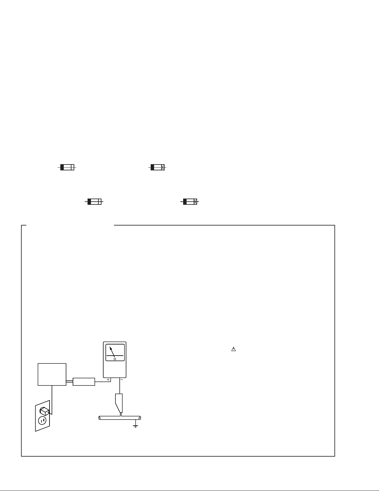
LEAKAGE CURRENT CHECK
Measure leakage current to a known earth ground (water
pipe, conduit, etc.) by connecting a leakage current tester
such as Simpson Model 229-2 or equivalent between the
earth ground and all exposed metal parts of the appliance
(input/output terminals, screwheads, metal overlays, control
shaft, etc.). Plug the AC line cord of the appliance directly
into a 120V AC 60Hz outlet and turn the AC power switch
on. Any current measured must not exceed 0.5mA.
Reading should
not be above
0.5mA
Earth
ground
Device
under
test
Also test with
plug reversed
(Using AC adapter
plug as required)
Leakage
current
tester
Test all
exposed metal
surfaces
ANY MEASUREMENTS NOT WITHIN THE LIMITS
OUTLINED ABOVE ARE INDICATIVE OF A POTENTIAL
SHOCK HAZARD AND MUST BE CORRECTED BEFORE
RETURNING THE APPLIANCE TO THE CUSTOMER.
2. PRODUCT SAFETY NOTICE
Many electrical and mechanical parts in the appliance
have special safety related characteristics. These are
often not evident from visual inspection nor the protection
afforded by them necessarily can be obtained by using
replacement components rated for voltage, wattage, etc.
Replacement parts which have these special safety
characteristics are identified in this Service Manual.
Electrical components having such features are identified
by marking with a
in this Service Manual.
The use of a substitute replacement component which does
not have the same safety characteristics as the PIONEER
recommended replacement one, shown in the parts list in
this Service Manual, may create shock, fire, or other hazards.
Product Safety is continuously under review and new
instructions are issued from time to time. For the latest
information, always consult the current PIONEER Service
Manual. A subscription to, or additional copies of, PIONEER
Service Manual may be obtained at a nominal charge from
PIONEER.
on the schematics and on the parts list
AC Leakage Test
2
Page 3
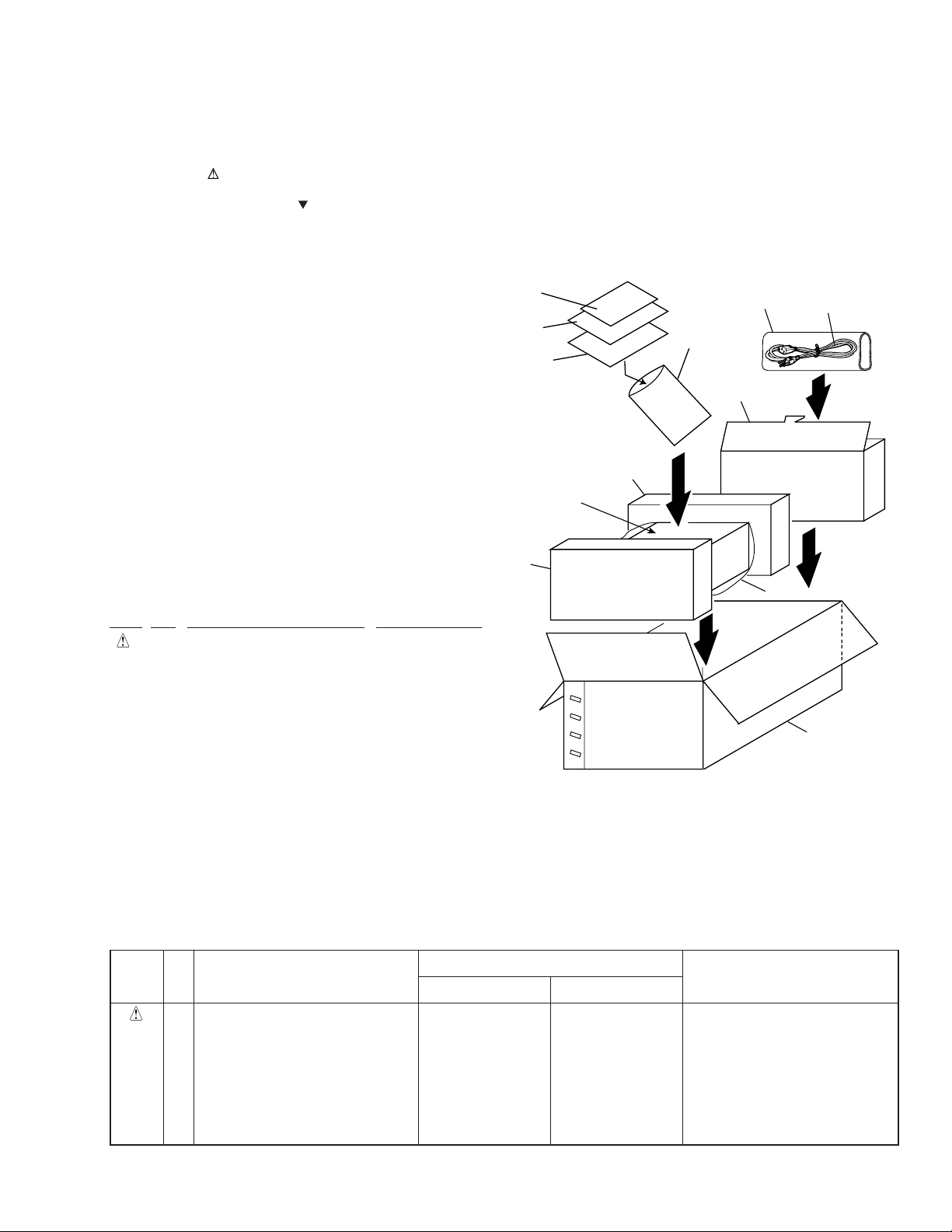
2. EXPLODED VIEWS AND PARTS LIST
NOTES:• Parts marked by "NSP" are generally unavailable because they are not in our Master Spare Parts List.
2.1 PACKING
The mark found on some component parts indicates the importance of the safety factor of the part.
•
Therefore, when replacing, be sure to use parts of identical designation.
Screws adjacent to mark on the product are used for disassembly.
•
CT-L11
(1) PACKING PARTS LIST
Mark No. Description Part No.
1 Power Cord
NSP 2 Warranty Card ARY7022
NSP
3 Operating Instructions
4 • • • •
5 Operating Instructions
6 Polyethylene Bag Z21–038
(0.03 × 230 × 340)
7 Pad Front AHA7340
8 Pad Rear AHA7341
9 Packing Case
10 Sheet (750 × 600 × 0.5) Z23–007
See Contrast table (2)
See Contrast table (2)
See Contrast table (2)
See Contrast table (2)
2
3
5
CT-L11
7
8
FRONT
12
1
6
11
10
9
11 Spacer N2001
12 Polyethylene Bag
(0.05 × 115 × 270)
See Contrast table (2)
See Contrast table (2)
(2) CONTRAST TABLE
CT-L11/MYXJ and NVXJ are constructed the same except for the following:
Mark
No.
1 Power Cord ADG1154 ADG1156
3 Operating Instructions ARE7279 Not used
5 Operating Instructions (English) Not used ARB7244
9 Packing Case AHD8000 AHD7999
11 Spacer N2001 Not used AHB7056
12 Polyethylene Bag Not used Z21-013
Symbol and Description
MYXJ type NVXJ type
(Swedish/Dutch/Portuguese/Spanish
/French/English/Italian/German)
Part No.
Remarks
3
Page 4
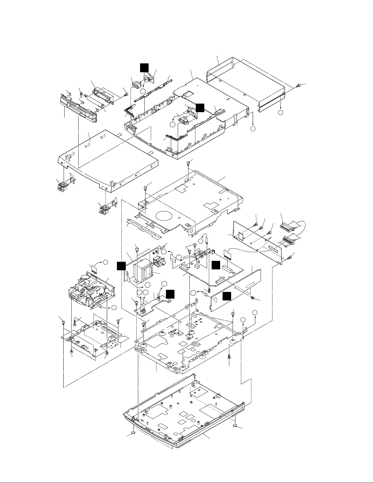
CT-L11
2.2 EXTERIOR
12
25
25
23
20
32
Refer to "2.3
DECK MECHANISM
UNIT"
34
38
28
18
14
34
30
D
5
21
27
34
F
25
16
22
6
31
E
22
37
37
33
7
20
29
35
3
A
24
37
A
D
F
9
F
37
B
34
19
D
4
E
34
1
C
E
B
C
C
40
21
B
17
15
A
34
H
G
41
8
37
34
34
2
40
H
G
11
36
36
13
39
10
13
26
4
Page 5

(1) EXTERIOR PARTS LIST
CT-L11
Mark No. Description Part No.
1 MAIN ASSY AWU7848
2 SIDE ASSY AWU7849
3 PRI ASSY AWU7850
4 TRADE ASSY AWU7851
5 KEY L ASSY AWU7852
6 KEY R ASSY AWU7853
7 16P FFC/60V(J2701) ADD7323
8 Cord With Plug(J2001) ADE7081
NSP 10 Bottom Plate ANF7027
NSP 15 Top Plate ANF7028
19 Power Transformer ATT7074
24 Fuse (FU2001:T250mA/250) REK1016
9 Deck Mechanism Unit TN-708CR-142R
11 Sub Chassis AND7040
12 TC Spring ABH7190
13 Leg AEB7090
14 TC Flap Holder AMR7315
16 TC Flap AAK7759
17 Rear Panel
18 Bonnet ANE7270
20 Sensor Plate ANG7360
21 Side Line AAP7088
22 Illuminate Lens AAK7896
23 Sub Panel TC Assy AXG7109
25 Cussion AEB7230
26 Bottom Base AMA7026
27 Top Panel 2 AMB7756
28 Top Panel 1 AMB7781
29 Lead Barrier AEC7361
30 Button L Assy AXG7110
See Contrast table (2)
Mark No. Description Part No.
31 Button R Assy AXG7111
32 Sensor Button L AAD7622
33 Sensor Button R AAD7623
34 Screw BPZ30P080FZK
35 Screw PBZ40P060FMC
36 Screw PMZ30P030FMC
37 Screw BBZ30P060FMC
38 Spacer AEC1065
NSP 39 PCB Holder PNW1706
NSP 40 PCB Spacer AEC7156
41 Screw VBZ30P080FZK
(2) CONTRAST TABLE
CT-L11/MYXJ and NVXJ are constructed the same except for the following:
Mark
No.
17 Rear Panel ANC8004 ANC8021
Symbol and Description
MYXJ type NVXJ type
Part No.
Remarks
5
Page 6
CT-L11
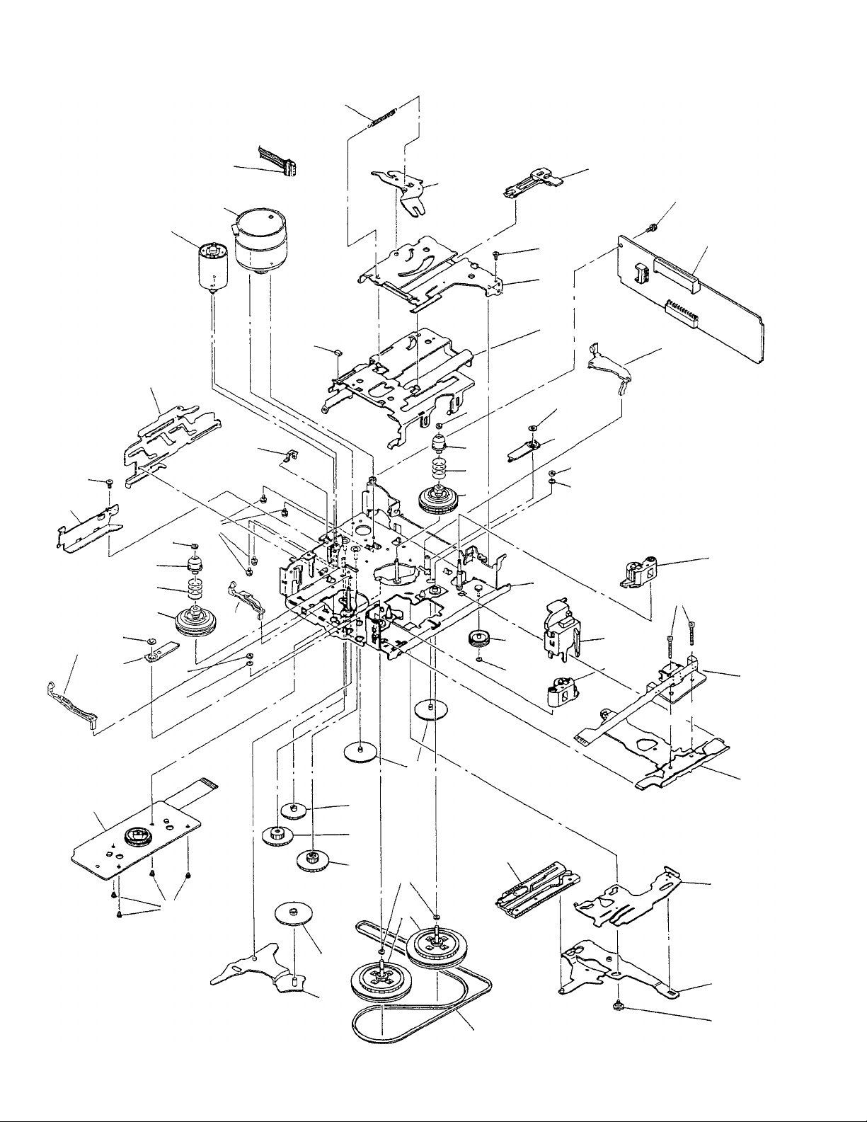
2.3 DECK MECHANISM UNIT
29
30
28
36
20
4
42
21
43
49
2
26
14
50
11
27
49
46
16
38
35
26
27
49
2
34
44
42
33
37
15
50
11
49
46
6
3
48
12
25
5
24
45
40
13
17
22
23
8
9
10
47
18
7
32
19
1
31
39
41
6
Page 7

÷ DECK MECHANISM UNIT PARTS LIST
Mark No. Description Part No.
1 PK Collar Screw A 18211223
2 Reel Cap 19500822
3 Middle Pulley 19501002
4 Wire Clumper 19501403
5 PEAR PWB (P) ASS'Y 1970-16-310
6 Chassis Rivet Assy 197001508
7 Main Plate 19700201
8 B Gear 19700202
9 C Gear 19700203
10 D Gear 19700204
11 P. G Plate 19700206
12 Guide BKT 19700207
13 P Gear W 19700212
14 REC Sensor F 19700213
15 REC Sensor R 19700214
16 CR Detective Plate H 19700215
17 Head Panel Assy 197003303
18 O.P Plate Assy 197004301
19 S.B Plate Rivet Assy 197004502
20 EJECT Lever Rivet Assy 197004504
CT-L11
21 O.P Plate Holder 197004707
22 FR Plate 19700601
23 FR Gear 19700602
24 Pinch Roller ARM (F) 197007303
25 Pinch Roller ARM (R) 197007304
26 Reel Wing Spring 19700812
27 Reel Assy (K) 197008302
28 SUB MOTOR ASS'Y 197009301
29 M Connector Assy 19701002
30 MAIN MOTOR ASSY(P) 197010303
31 Main Belt (G) 19701106
32 FL Capstan Assy 197011301
33 Case Lifter B 19701201
34 Pack Slider 19701203
35 P.S Actuator Plate 19701204
36 Cushion Rubber 19701206
37 Cassette Case R 19701216
38 P.S Spring (P) 19701219
39 REEL PWB ASSY 197013312
40 RPE AC-5544BM-5949 62010502
41 Camera Screw 2.0x2.5 9C0420253
42 Camera Screw 2.0x3.0 9C0420303
43 Tams Screw 2.0x3.0 9P0220031
44 Tams Tapping Screw 9P12-20-051
45 Screw 2.6x4.0 9P1420042
46 P. Washer 2.1x3.5x0.2 9W0120050
47 P. Washer 2.1x3.5x0.35 9W0135010
48 P. Washer 0.85x2.8x0.2 9W0225010
49 P. Washer 1.55x3.5x0.5 9W0250040
50 Hlw Washer 2.1x4.0x0.2 9W0635020
7
Page 8
1
23
CT-L11
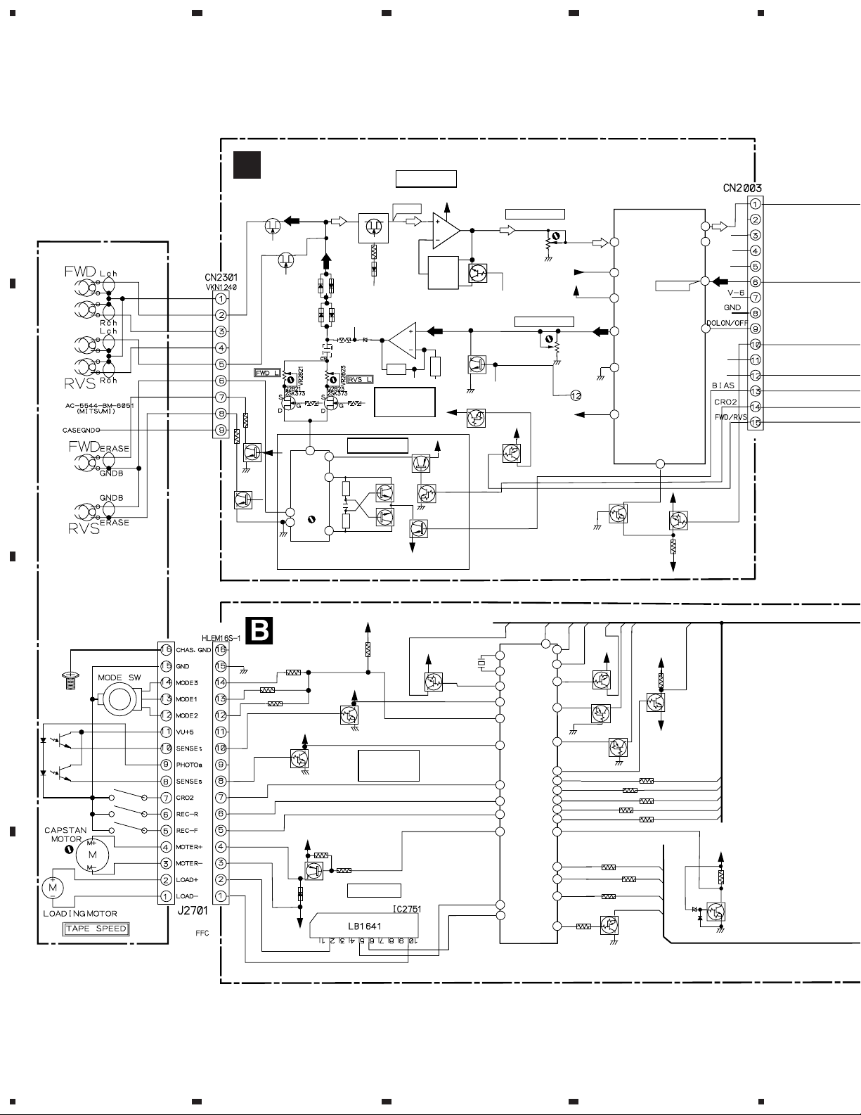
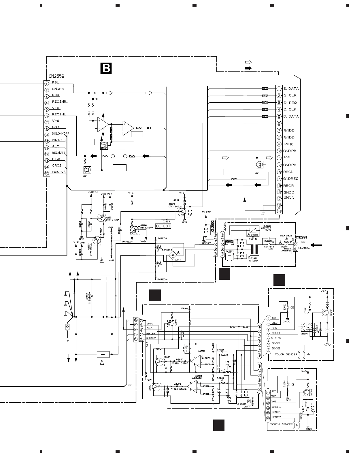
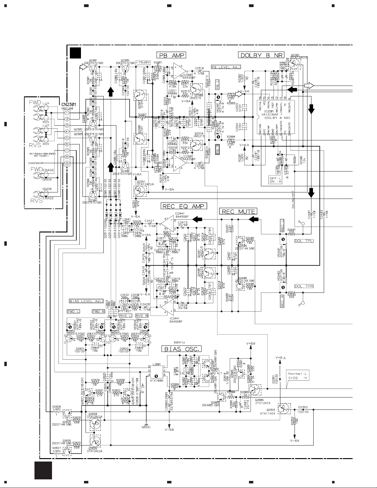
3. BLOCK DIAGRAM AND SCHEMATIC DIAGRAM
3.1 BLOCK DIAGRAM and OVERALL SCHEMATIC DIAGRAM
4
A
SIDE ASSY
A
: AWU7849
2
1
3
Q2305
2SK373
D
D
IC2441(1/2)
BA4558F
BIAS OSC
2SC2412K
Q2301
2SK373
Q2303
2SK373
REC/PB
HEAD
B
ERACE
HEAD
DECK
GNDB
Q2826
2SD211K
Q2825
2SD2114K
#
GNDB
ATX7006
5
4
6
L2801
MECHANISM
S
S
G
G
REC EQ
Q2801
2SC2412K
Q2802
PB AMP
-76dBv
AMP
V-6B
GNDA
2SC2412K
5
6
BIAS
V+6A
IC2301(1/2)
BA4558F
8
8
7
EQ
EQ
REC MUTE
GNDA
#
V+6B
Q2805
2SA1037
Q2806
DTC124EK
Q2803
Q2309
DTC114TK
Q2405
2SD2114K
Q2830
DTA124EK
Q2353
DTA114EK
PB LEVEL ADJ.
VR2301
VCP1154
4.7K-B
REC LEVEL ADJ.
RECMUTE
V+6A
XCrO2
BIAS
GNDA
V+6A
VR2401
VCP1156
10K-B
GNDA
RECMUTE
PB IN R
GNDA
REC
OUT
R
GNDA
PB IN L
14
3
ACC
2
HA12136AF
DOLBY-B NR
9
4
8
Q2202
DTA124EK
IC2201
REC/PB
12
-32.2dBv
LINE
OUT L
V+6A
V-6A
11
6
16
5
PB/XREC
RECMUTE
Q2354
DTA124EK
UNIT
TN-708CR-142R
CN2556
MAIN ASSY
: AWU7848
GNDC
C
SENSEt
Q2701
DTC143EK
V+5U
SENSEs
Q2702
DTC143EK
GNDD
V+6M
Q2751
2SB1425
ADD7323
V-6M
V+5U
GNDD
LOADING
V+5U
MECHA
CONT
XMOTOR
V+6A
X2501
VSS1045
6MHz
FWD/REV
CrO2(SW)
XREC-R
XMOTOR
SENSE1
MODE
SENSE2
XREC-F
LOAD1
LOAD2
10
11
47
23
17
25
20
19
22
3
40
41
REC
MUTE
IC2501
PDC081A
µ-COM
44
V+6A
15
MS
43
PB/XREC
XCrO2
45
Q2355
DTA124EK
BIAS
46
GNDC
DOL ON/OFF
39
GNDC
PBMUTE
37
DCLK DCLK
36
DREQ DREQ
38
SCLK
4
SDATA
28
DDATA
34
XRESET
5
LED REC
32
LEDRVSM
31
KEY
13
Q2552
DTA124EK
1
GNDC
V+9
V-6A
BLUELED
Q2154
DTC124EK
Q2531
DTC143EK
PBMUTE
SCLK
SDATA
DDATA
+
GNDC
V+5
D
8
1234
Page 9
5
678
CT-L11
Note : When ordering service parts, be sure to refer to "EXPLODED VIEWS and PARTS LIST" or "PCB PARTS LIST".
IC2121(1/2)
BA4558F
ALC
2SC2412K
Q2123
2SC2412K
GNDA
+
+
5
6
V+6A
MAIN ASSY
: AWU7848
V+6A
8
7
4
V-6A
F2101
RTF1209Q2121
MPX
MPX
3
2
36
IC2121(2/2)
BA4558F
1
MS
PB Lch
MS
REC L ch
S. DATA
S. CLK
D. REQ
D. CLK
D. DATA
GND PB
PB L ch
PB MUTE
REC L ch
Q2153
2SD2144k
PB MUTE
V+12V
:PLAYBACK SIGNAL ROUTE
:RECRDING SIGNAL ROUTE
CN2555
PROTECT
GNDA
GNDRY
V+12RY
GNDRY
A
B
TO MJ(MJ-L11) or CD TUNER(XC-L11)
V+6
GNDC
GNDM
GNDB
CHASSIS
GND
V-6 V-6M
V+6M
IC2013
NJM7806FA
INOUT
IC2014
NJM7906A
AC IN
AC CORD
INOUT
F
PRI ASSY
:AWU7850
D
KEYL ASSY
:AWU7852
C
TRADE ASSY
E
:AWU7851
V+5
CN2553
GNDC
J2902
J2554
J2581
STOP
PLAY
FWD/REV
D
OPEN/
CLOSE
KEYR ASSY
C
:AWU7853
9
5
6
7
8
Page 10
1
23
CT-L11
3.2 SIDE, MAIN (1/2), KEYR and KEYL ASSYS
SIDE ASSY (AWU7849)
A
A
DECK
MECHANISM
UNIT
(TN-708CR-142R)
B
4
C
D
10
A
1234
Page 11

5
678
CT-L11
B 1/2
MAIN ASSY (AWU7848)
SIGNAL ROUTE
: PLAYBACK SIGNAL
: RECORDING SIGNAL
A
B 2/2
B
C
KEYR ASSY
(AWU7853)
J2581
E
KEYL ASSY
D
(AWU7852)
: The power supply is shown with the marked box.
KEYL ASSY
S2592 : REC/ PAUSE
Touch FWD/REV
Sencer
KEYR ASSY
S2581 : STOP
Touch : OPEN/CLOSE
Sencer
J2554
E
C
D
B 1/2
5
6
7
C
D
8
11
Page 12

1
23
CT-L11
3.3 MAIN (2/2), TRADE and PRI ASSYS
A
(TN-708CR-142R)
B
4
ADD7323
C
J2554
D
J2581
C
LIVE
NEUTRAL
AC POWER CORD
ADG1154
or ADG1156
AC220-230V/50Hz
TRADE ASSY
E
(AWU7851)
F
D15A05-150-2651
J
PLOTECT
PRI ASSY
(AWU7850)
250mA
J2002
D
12
B 2/2
1234
E
F
Screw Terminal
1948
Page 13

5
B 2/2
MAIN ASSY (AWU7848)
678
CT-L11
SIGNAL ROUTE
: PLAYBACK SIGNAL
: RECORDING SIGNAL
A
6.3V
CHECK POINT for Service
B 1/2
B
C
–6.3V
: The power supply is shown with the marked box.
5
6
To MJ(MJ-L11) or CD TUNER (XC-L11)
7
B 2/2
8
D
13
Page 14

1
23
CT-L11
4. PCB CONNECTION DIAGRAM
4.1 SIDE ASSY
A
A
SIDE ASSY
NOTE FOR PCB DIAGRAMS:
1. Part numbers in PCB diagrams match those in the schematic
diagrams.
2. A comparison between the main parts of PCB and schematic
diagrams is shown below.
Symbol in PCB
Diagrams
BCE
BCE
B
DGS
Symbol in Schematic
Diagrams
BCE
BCEBCE
DGSDGS
BCE
Part Name
Transistor
Transistor
with resistor
Field effect
transistor
Q2304
Q2302
Q2301
Q2303
Q2821
Q2822
Q2824
Q2823
Q2306
Q2305
VR2821
VR2823
4
SIDE A
To DECK
Mechanism
VR2822
VR2824
Resistor array
3-terminal
regulator
3. The parts mounted on this PCB include all necessary parts
for several destination.
For further information for respective destinations, be sure
to check with the schematic diagram.
4. Viewpoint of PCB diagrams
CapacitorConnector
SIDE A
P. C. Board Chip Part
SIDE B
C
VR2402
VR2401
VR2302
VR2301
B
CN2559
D
(ANP7411-B)
14
A
1234
Page 15

1
A
SIDE ASSY
234
CT-L11
SIDE B
A
Q2802
Q2805
Q2825
Q2826
Q2829
Q2830
Q2801
Q2803
Q2806
Q2827
Q2308
Q2307
IC2301
Q2309
Q2310
IC2441
Q2407
Q2408
Q2405
Q2406
Q2351
Q2354
B
C
Q2202
Q2353
IC2201
D
(ANP741-B)
A
1
2
3
4
15
Page 16

1
CT-L11
4.2 MAIN ASSY
23
4
A
MAIN ASSY
B
B
To DECK MECHANISM
SIDE A
E
CN2902
A
CN2003
C
To CD TUNER XC-L11
IC2751
IC2015
(ANP7411-B)
D
IC2013
IC2014
16
B
1234
Page 17

1
234
CT-L11
MAIN ASSY
B
SIDE B
Q2557
Q2552
Q2352
Q2804
Q2355
Q2153
Q2154
Q2703
Q2753
Q2752
Q2201
Q2704
Q2701
IC2561
IC2581
Q2123
Q2562
Q2561
Q2501
A
B
(ANP7411-B)
Q2121
Q2531
Q2122
IC2121
Q2054
Q2053
Q2051
Q2052
C
Q2151
Q2152
D
1
2
3
4
B
17
Page 18

CT-L11
1
23
4
4.3 KEYL, KEYR, TRADE and PRI ASSYS
A
B
C
KEYR ASSY
PRI ASSY
F
AC IN CORD
D
KEYL ASSY
(ANP7411-B)
TRADE ASSY
E
SIDE A
C
IC2011
IC2012
D
(ANP7411-B)
(ANP7411-B)
B
CN2553
B
CN2002
18
C
D E
1234
F
Page 19

F
PRI ASSY
Q2591 Q2592
Q2581
Q2902
Q2901
Q2582
IC2901
ANP7411-B
(ANP7411-B))
(ANP7411-B)
D
KEYL ASSY
C
KEYR ASSY
E
TRADE ASSY
1
234
CT-L11
SIDE B
A
B
C
1
C
2
3
D E
F
4
19
D
Page 20

CT-L11
Mark No. Description Part No.
Mark No. Description Part No.
5. PCB PARTS LIST
NOTES:•Parts marked by "NSP" are generally unavailable because they are not in our Master Spare Parts List.
Mark No. Description Part No.
LIST OF PCB ASSEMBLIES
NSP TC COMP AWM7632
The mark found on some component parts indicates the importance of the safety factor of the part.
•
Therefore, when replacing, be sure to use parts of identical designation.
When ordering resistors, first convert resistance values into code form as shown in the following examples.
•
Ex.1 When there are 2 effective digits (any digit apart from 0), such as 560 ohm and 47k ohm (tolerance is shown by J=5%,
and K=10%).
560 Ω→56 × 10
47k Ω→47 × 10
1
→ 561 ........................................................ RD1/4PU 5 6 1 J
3
→ 473 ........................................................ RD1/4PU 4 7 3 J
0.5 Ω→R50 ..................................................................................... RN2H R 5 0 K
Ex.2 When there are 3 effective digits (such as in high precision metal film resistors).
5.62k Ω→ 562 × 10
1
→ 5621 ......................................................RN1/4PC 5 6 2 1 F
1 Ω→1R0 ..................................................................................... RS1P
1 R 0
K
Mark No. Description Part No.
C2425, C2426 CEAT101M10
C2103, C2104, C2401, C2402 CEAT1R0M50
C2807 CEAT220M50
MAIN ASSY AWU7848
SIDE ASSY AWU7849
PRI ASSY AWU7850
TRADE ASSY AWU7851
KEYL ASSY AWU7852
KEYR ASSY AWU7853
C2313, C2314, C2419, C2420 CEAT330M50
C2805, C2806 CEAT330M50
C2319, C2320, C2427, C2428 CEAT4R7M50
C2205, C2206 CEATR22M50
C2417, C2418 CFTLA154J50
C2801 CFTLA183J50
C2429, C2430 CKSRYB122K50
SIDE ASSY
A
SEMICONDUCTORS
IC2301, IC2441 BA4558F-HT
IC2201 HA12136AF
Q2805 2SA1576A
Q2802 2SC2412K
Q2827, Q2828 2SC3138
Q2801, Q2803 2SC4081
Q2405, Q2406, Q2825, Q2826 2SD2114K
Q2301-Q2306, Q2821-Q2824 2SK373
Q2353 DTA114EUA
Q2829, Q2830 DTA124EK
Q2202, Q2351, Q2354 DTA124EUA
Q2309, Q2310, Q2407, Q2408 DTC114TK
Q2806 UN5212
D2301-D2304, D2309, D2310 1SS133
D2351, D2352, D2821, D2822 1SS133
D2305-D2308, D2311-D2314 1SS355
D2825 S5688G
COILS AND FILTERS
L2801 OSC COIL ATX7006
L2441, L2442 18MHz Coil RTF1027
CAPACITORS
C2823, C2824 CCSQCH101J50
C2421, C2422 CCSQCH152J50
C2301-C2306, C2821, C2822 CCSRCH100D50
C2309, C2310, C2825 CCSRCH101J50
C2431, C2432 CCSRCH391J50
C2307, C2308, C2413-C2416 CCSRCH681J50
C2203, C2204 CEAT100M50
C2201, C2202, C2315, C2316 CEAT101M10
C2803, C2804 CKSRYB472K50
C2820 CQHA472J2A
C2802 CKSRYB682K50
C2311, C2312 CQMA682J50
C2411, C2412 CQMBA103J50
RESISTORS
R2827, R2828 RD1/4PU1R0J
R2317, R2318 RD1/4PU471J
R2201, R2202, R2423, R2424, R2810 RD1/4PU820J
R2803 RD1/4PU8R2J
R2983, R2984, R2991, R2998 RS1/10S0R0J
R2824 RS1/10S105J
VR2301, VR2302 VCP1154
VR2401, VR2402 VCP1156
VR2821-VR2824 VCP1162
Other Resistors RS1/16S&&&J
OTHERS
CN2003 15P SOCKET KP200TA15L
CN2301 9P FFC CONNECTOR VKN1185
MAIN ASSY
B
SEMICONDUCTORS
IC2121 BA4558F-HT
IC2013 NJM7806FA
IC2015 NJM78M05FA
IC2014 NJM7906FA
IC2751 LB1641
IC2501 PDC081A
Q2751 2SB1425
Q2121, Q2123, Q2124, Q2703 2SC4081
Q2121, Q2152 2SD2114K
Q2352 DTA114EUA
20
Page 21

CT-L11
Mark No. Description Part No.
Q2051,Q2053,Q2153,Q2201,Q2355 DTA124EUA
Q2552, Q2804 DTA124EUA
Q2752, Q2753 DTA143EUA
Q2531, Q2701, Q2702 DTC143EUA
Q2122 DTC144EUA
Q2052,Q2054,Q2154,Q2501,Q2557 UN5212
Q2704 UN5212
D2012 11EQS06
D2051-D2053,D2056-D2059,D2532 1SS133
D2701, D2702, D2751 1SS133
D2011 D2SBA20(B)
D2121-D2125, D2131 1SS355
D2754 MTZJ4.3B
D2054 MTZJ4.7B
D2055 MTZJ6.8B
D2571,D2572,D2573,D2574,D2575 MTZJ8.2B
D2015 S5688G
COILS AND FILTERS
F2101, F2102 MPX FILTER RTF1209
L2501 LFEA221J
X2501 CERAMIC RES. (6MHz) XSS3001
CAPACITORS
C2513, C2514 CCSRCH470J50
C2024, C2531 CEAT100M50
C2019, C2020, C2505 CEAT101M10
C2017, C2018, C2023, C2132 CEAT1R0M50
C2207, C2208, C2451 CEAT1R0M50
C2013, C2014 CEAT332M25
C2121 CEAT220M50
C2751 CEAT471M16
C2122, C2133 CKSQYF105Z16
C2025, C2501, C2502, C2509 CKSRYB102K50
C2503,C2504,C2506-C2508,C2755 CKSRYB103K50
C2754 CKSRYB104K16
C2510, C2511 CKSRYB221K50
C2101, C2102 CQMBA103J50
RESISTORS
R2754 RS1LMF2R2J
Other Resistors RS1/16S&&&J
OTHERS
2003 5P CABLE HOLDER 51048-0500
CN2555 19P CABLE CONNECTOR AKP7002
J2902 JUMPER WIRE D15A05-150-2651
CN2556 16P FFC CONNECTOR HLEM16S-1
CN2559 15P PLUG KM200TA15
CN2553 5P JUMPER CONN. KPE5
2004 SCREW TEMINAL VNE1948
KN2001 EARTH METAL FITTING VNF1084
PRI ASSY
F
SEMICONDUCTORS
D2001 1SS133
Mark No. Description Part No.
CAPACITORS
C2001, C2002 ACE7013
C2003, C2004 CKSRYF103Z50
C2005, C2006 CQMBA473J50
OTHERS
2002 5P CABLE HOLDER 51048-0500
H2001, H2002 FUSE CLIP AKR7001
J 2002 JUMPER WIRE D20PYY0525E
AN2001 AC INLET XKP3041
TRADE ASSY
2001 PCB BINDER VEF1040
E
SEMICONDUCTORS
IC2901 NJM062M
Q2581 2SA1576A
Q2901, Q2902 DTC114TUA
D2901-D2910 1SS133
COILS AND FILTERS
L2902 LCTAR22J2520
CAPACITORS
C2903 CEAT470M25
C2905, C2906 CEAT4R7M50
C2901, C2902 CKSRYB102K50
C2904 CKSRYB103K50
RESISTORS
Other Resistors RS1/16S&&&J
OTHERS
2902 5P CABLE HOLDER 51063-0505
2953 6P CABLE HOLDER 51063-0605
2901 7P CABLE HOLDER 51063-0705
KN2901 EARTH METAL FITTING VNF1084
KEYL ASSY
D
SEMICONDUCTORS
Q2592 2SA1576A
Q2591 UN5212
D2592 E1L55-3B0A
D2591 SLR-343VC(NPQ)
SWITCHES AND RELAYS
S2591 ASG7013
CAPACITORS
C2591 CKSRYF104Z25
RESISTORS
Other Resistors RS1/16S&&&J
OTHERS
2554 7P JUMPER WIRE 51063-0705
J2554 7P CABLE HOLDER D15A07-100-2651
COILS AND FILTERS
L2001 XTF3001
SWITCHES AND RELAYS
RY2001 ASR7013
21
Page 22

CT-L11
Mark No. Description Part No.
KEYR ASSY
C
SEMICONDUCTORS
Q2582 2SA1576A
D2581 E1L55-3B0A
SWITCHES AND RELAYS
S2581 ASG7013
CAPACITORS
C2582 CKSRYF104Z25
RESISTORS
Other Resistors RS1/16S&&&J
OTHERS
2581 6P JUMPER WIRE 51063-0605
J2581 6P CABLE HOLDER D15A06-300-2651
Mark No. Description Part No.
22
Page 23

6. ADJUSTMENT
For adjustment, use the STEREO CD RECEIVER (XC-L11) in combination with the DISPLAY UNIT(AXX7107).
6.1 TEST MODE
How to Enter the Test Mode
In case of system operation ........
Receive “A15F” (bus data 1C5F) with the remote control or switch on the power with the TEST MODE JP [W157 (GNDC) and W1538
(TEST)] of the MAIN ASSY short-circuited (pin 30 of the microcomputer connected to GND).
(Refer to Fig. 6-1.)
In case of single operation ........
Connect part A of the MAIN ASSY [W263 (GNDA) and W105 (GNDC) ], short-circuit the TEST MODE JP [W157 GNDC) and
W158 (TEST)] (pin 30 of the microcomputer connected to GND), short-circuit JP the PRI ASSY [W152 and W180] and supply AC
power cord to connect. (Refer to Fig. 6-1.)
* Single operation the keys “EJECT” , "STOP", "REC" and “PLAY” operate normally, and other connect part B
of the TRADE ASSY W260 (GNDC), short-circuit the TEST JUMPER [W111(REW) and W112(FF)].
CT-L11
TRADE ASSY
For Service Jumper Wire
GNDC
W260
REW
W111
F F
W112
FRONT
TEST MODE
MAIN ASSY
Short point
W158
W157
B
W261 ...... RECR
W262 ...... RECL
W265 ...... PBL
W266 ...... PBR
A
Fig. 6–1
23
Page 24

CT-L11
6.2 SINGLE OPERATION METHOD
Operation of the Test Mode
1. When the “EJECT” key is pressed, cassette mechanism switch
check mode is entered and the DISPLAY Part displays the
following.
REV REC SW
ON: REV recording possible R
OFF: Impossible –
FWD REC SW
ON: FWD recording possible F
OFF: Impossible –
TAPE TYPE
NORMAL (TYPE I) 1
CrO2 (TYPE II) 2
2. When the “REC PAUSE” key is pressed, the mode for opening
of REC PLAY is reached, automatic recording and playback
mode is reached and the following operation is performed.
1 FUNCTION is set to AUX.
2 FWD recording is performed for 4 sec.
3 RVS recording is performed for 4 sec.
4 FWD playback is performed for 4 sec. (Function becomes
TAPE), and the unit stops.
6 STOP.
LINE MUTE opens in REC condition.
Operation of preparation
Connect part A of the MAIN ASSY [W105(GNDC) and
W263 (GNDA)], short-circuit the TEST MODE JP [W157
GNDC) and W158 (TEST)] (pin 30 of the microcomputer
connected to GND), and supply AC power cord to connect.
In case of single connect load
In case of adjustment as a single unit, connect a 27 kΩ load
resistor to pins W266(PBR) and W265(PBL) of (MAIN
ASSY ). (Refer to Fig. 6-4.)
In case of input signal
In case of adjustment as a single unit, enter the signal at
W262(REC_L) and W266(REC_R) of MAIN ASSY. At this
time, connect an output buffer amplifier to the oscillator, and
then connect a series resistor(180 Ω) after the impedance
hasbecome sufficiently low. (For MPX filter impedance
matching) (Refer to Fig. 6-4.)
In case of Fuction
Connect part B of the TRADE ASSY[ “REW”(W111) and
“FF”(W112) circuit the TEST JUMPER [W260 GNDC] .
REW
GNDC
W260
W111
F F
W112
3. "DOLBY" ON/OFF check mode is made with the main part "
STOP" key.
4. The remote control the keys “PLAY”, “FF”, “RWD”, “STOP”,
and “REC” operate normally and LINE MUTE opens in REC/
REC PAUSE condition.
7 Cancellation of test mode
Press the “STANDBY/ON” key or disconnect the AC power
supply.
24
Page 25

6.3 ADJUSTMENT
Please execute this adjustment in test mode .
CT-L11
Adjustment Condition
(1) The ground at the time of adjustment shall be W134.
(Refer to Fig. 6–4).
(2) Clean the heads and demagnetize them using a head eraser.
(3) Set the measurement level to 0 dBV = 1 Vrms.
(4) Use the specified tape for adjustment. Use the labeled (A) side
of the test tape.
NCT–111 : For Tape Speed Adjustment
: For Head Azimuth Adjustment
NCT–132X : For Playback Level Adjustment
: For Playback Frequency Adjustment
STD–633 : Normal blank tape
STD–622 : CrO
(5) Provide yourself with the following measuring devides:
• AC millivoltmeter
• Low-frequency oscillator
• Attenuator
• Oscilloscope
(6) Adjust both right and left channels unless otherwise specified.
(7) Turn the DOLBY NR switch off unless otherwize specified.
(8) Warm up the unit for several minutes before adjustment. In
particular, be sure to warm up the unit in the REC/PLAY mode
for 3 to 5 minutes before starting recording/playback frequency
characteristics adjustment.
(9) Always follow the indicated adjustment order.
Otherwise, a complete adjustment may not be achieved.
2 blank tape
List of Adjustment
¶ Playback Section
(1) Tape Speed No Adjustment (Confirmation)
(2) Head Azimuth Confirmation
(3) Playback Level Adjustment FWD
REV Confirmation
(4) Playback Frequency Characteristics Confirmation
¶ Recording Section
(1) Recording Bias Adjustment FWD
(2) Recording Bias Adjustment REV
(3) Recording Level Adjustment FWD
REV Confirmation
PLAY BACK
250
3dB
RECORDING
12.5k
10k
3dB 4dB
Dolby noise reduction manufactured under license from Dolby
Laboratories Licensing Corporation.
“DOLBY” and the double-D symbol are trademarks of Dolby
Laboratories Licensing Corporation.
Test Tape NCT-132X
0 dB
30s
315 Hz
0 dB: 315 Hz, 250 nwb/m
30 s 30 s 30 s 10s 10s .......................................................................................................... 10s
6.3 kHz 10 kHz 315 Hz 14 kHz
Fig. 6-3 Test Tape NCT-132X
12.5
kHz
10 kHz
8 kHz 4 kHz2 kHz
250
3dB
Fig. 6-2 Frequency Characteristics
6.3
kHz
1 kHz
500Hz250Hz125
10k
3dB
Hz
12.5k
5dB
–20 dB
63 Hz 40 Hz
25
Page 26

CT-L11
6.3.1 Playback Section
(1) Tape Speed Confirmation
No. Mode Input Signal/Test Tape Adjustment Points Measurement Points Adjustment Value Remarks
PLAY1
NCT-111 (3 kHz)
No Adjustment
PB OUT
(PBR:W266)
(MAIN ASSY)
(2) Head Azimuth Confirmation
• This unit is equipped with auto tape selector.
• Do not switch between forward and reverse operation with the screwdriver inserted.
No. Mode Input Signal/Test Tape Adjustment Points
Measurement
3000 Hz+90Hz
- 60Hz
Points
REV Confirmation
( 3000 Hz + 90Hz )
– 60Hz
Remarks
PLAY1
NCT-132X
(10 kHz, –20dB)
Head azimuth
No adjustment
PB L cH(W265)
PB R cH(W266)
(MAIN ASSY)
(3) Playback Level Adjustment
• Since this adjustment determines playback DolbyNR level, Perform it carefully.
No. Mode Input Signal/Test Tape Adjustment Points
PLAY1
NCT-132X test tape
(Playback: 315 Hz, 0 dB)
L ch
R ch VR2302
VR2301
Measurement
Points
PB L cH(W265)
PB R cH(W266)
(MAIN ASSY)
Adjustment
Value
–6.0 dBV
(4) Playback Frequency Characteristics Confirmation
No. Mode Input Signal/Test Tape Adjustment Points
1
PLAY
NCT-132X test tape
Measurement
Points
PB L cH(W265)
PB R cH(W266)
(MAIN ASSY)
Adjustment
Value
6.3.2 Recording Section
(1) Recording Bias Adjustment
• After the adjustment, caution should be exercised so as not to become under bias by checking the distortion rate.
No. Mode Input Signal/Test Tape Adjustment Points
1
*
REC =
2
PLAY
Input a 315Hz (-26dBv)signal to
the REC IN terminal .
(W262:REC L) (W261: REC R)
Load the STD–633 test tape and
record/playback the 315Hz and
10kHz signals. (see the Note below)
Input signal level
FWD.VR2821
L ch
R ch FWD.VR2822
Measurement
Points
PB L cH(W265)
PB R cH(W266)
(MAIN ASSY)
REV.VR2823
REV.VR2824
Adjustment
Value
–26 dBV
Repeat adjustment until playback level of
the 10kHz signal is within -0.5dB ± 0.5dB
from that of the 315Hz signal.
FWD / REV
Confirmation
Remarks
FWD Adjstment
REV Confirmation
( – 6.0 dBv ± 2.0dB )
Remarks
Check that the frequency
characteristics is within the
range of Fig. 6-2.
Remarks
Note: Set the 10kHz input signal level to the same value as the 315Hz input signal level of step 1.
(2) Recording Level Adjustment
No. Mode Input Signal/Test Tape Adjustment Points
1
*
REC =
2
PLAY
Input a 315Hz (-10dBv)signal to
the REC IN terminal .
(W262:REC L) (W261: REC R)
• STD–633 test tape and record/
playback the 315Hz signal.
• DOLBY NR : OFF
Input signal level –10 dBV
L ch
R ch VR2402
VR2401
Measurement
Points
PB L cH(W265)
PB R cH(W266)
(MAIN ASSY)
Adjustment
Value
Repeat recording, playback and
adjustment until playback level of the
315Hz signal becomes –
Remarks
10dBV ± 0.5dB
.
*: In case of adjustment as a single unit, enter the signal at W262(RECL)and W261(RECR) ofMAIN ASSY. At this time, connect an output
buffer amplifier to the oscillator, and then connect a series resistor (180 Ω) after the impedance has become sufficiently low. (For MPX
filter impedance matching)
26
Page 27

CT-L11
Adjustment and Measurment Points
W261 ...... RECR
W262 ...... RECL
W265 ...... PBL
W266 ...... PBR
PB LEVEL
VR2302
(R ch)
VR2301
(L ch)
MAIN ASSY
TEST MODE
VR2821
(FWD:L ch)
VR2822
(FWD:R ch)
VR2823
(REV:L ch)
VR2824
(REV:R ch)
REC LEVEL
VR2401
VR2402
(R ch)
BIAS LEVEL
(L ch)
Front
SIDE ASSY
Fig. 6–4 Adjustment and Measurement Points
27
Page 28

CT-L11
7. GENERAL INFORMATION
7.1 DIAGNOSIS
7.1.1 DISASSEMBLY
Bonnet, Top Panel 1, Top Panel 2 and Top Plate
3
hook
Bonnet
3
Illuminate Lens
3
KEYR Assy
4
KEYL Assy
Illuminate Lens
2
1
2
Top Panel 1
1
1
Top Panel 2
1
hook
1
2
1
28
Illuminate
Lens
Illuminate
2
2
Lens
1
1
Top Plate
1
1
1
Page 29

CT-L11
1
Remove Sub Panel TC Assy
3
Disconnect the 16P FFC/30V
(J2701)
2
2
2
2
Remove the four screws
4
Disconnect the Flexible Flat Cable
(CN2301)
PCB Location
PRI ASSY
F
TRADE ASSY
E
KEYL ASSY
D
KEYR ASSY
C
SIDE ASSY
A
MOTHER ASSY
B
29
Page 30

CT-L11
7.1.2 POWER ON SEQUENCE
• STANDBY/ON key is pressed.
• Receive the system power on
information with the sytem bus.
Go to Power ON
500mS WAIT
M_ MODE :
STOP ?
M_MODE : Pin No. 17
No
Yes
Is MODE SW
OFF ?
Yes
LOAD2 100mS ON
LOAD2 :
Pin No.41
No
LOAD2 ON
M_MODE :
EJECT ?
No
Is it second
times ?
Yes
:Give up
LOAD2 OFF
Yes
No
30
Mechanism Initializa end.
END
Page 31

7.2 PARTS
No. Pin Name I/O Pin Function No. Pin Name I/O Pin Function
1 DIMR 1 O BLUE LED Dimmer control 1 25 SENSE 2 I Sensing pulse input 2
2 DIMR 2 O BLUE LED Dimmer control 2 26 NC − Not used
3 XMOTOR O Cassette mechanism main motor control 27 S.DOUT O System bus output data
4 S.CLK I System bus clock 28 S.DIN I System bus input data
5 XRESET I Reset input 29 NC − Not used
6 E+5V I Connect to V
DD
30 XTEST I Test mode detection input
7NC − Not used 31 NC − Not used
8 E+5V I Connect to V
DD
32 LEDREC O Dir LED(REC) ON/OFF
9 GNDC − GND 33 NC − Not used
10 CF1 I
Connected to ceramic oscillator ( 6 MHz)
34 D.DATA O Display bus Data control
11 CF2 O 35 NC − Not used
12 E+5V − Power supply +5V 36 D.CLK O Display bus Clock control
13 KEY1 I
AD key data input
37 XPB MUTE O PB MUTE control
14 E+5V − 38 D.REQ I Display bus Request
15 MS I MS audio signal input 39 DOLBY O DOLBY NR control
16 NC − Not used 40 LOAD 1 O
Loader mechanism motor close control (+)
17 XMODE I Cassette mechanism mode SW input 41 LOAD 2 O
Loader mechanism motor close control (–)
18 NC − Not used 42 NC − Not used
19 XRECR I REV REC detection SW input 43 PB/XREC O DOLBY PB/REC control ON/OFF
20 XCrO
2
(SW) I CrO2 position detection SW input 44 RECMUTE O REC MUTE control
21 NC – Not used 45 XCrO
2
O Normal / CrO2 control
22 XRECF I FWD REC detection SW 46 BIAS O BIAS control
23 SENSE 1 I Sensing pulse input 1 47 XFWD/RVS O Head (FWD/RVS)SNLG Switch
24 NC − Not used 48 NC − Not used
Connect to V
DD
7.2.1 IC
• The information shown in the list is basic information and may not correspond exactly to that shown in the schematic diagrams.
PDC081A (MAIN ASSY : IC2501)
• System Microcomputer
Pin Function
•
CT-L11
31
Page 32

CT-L11
8. PANEL FACILITIES AND SPECIFICATIONS
PANEL FACILITIES
23
PLAY (touch sensor)
¶8 RECORD PAUSE
PLAY
23
¶8
!
REC PAUSE
DOLBY* NR
*
Dolby noise reduction manufactured under license from
Dolby Laboratories Licensing Corporation.
“DOLBY” and the double-D symbol are trademarks of
Dolby Laboratories Licensing Corporation.
0 EJECT (touch sensor)
Cassette loading slot
SPECIFICATIONS
System ......................................................4-track, 2-channel stereo
Heads.................................................................... “Hard Permalloy”
Motor ................................................................ DC servo motor x 1
Wow and Flutter................................. *0.08% (WRMS) /0.14%(DIN)
Frequency Response
–20 dB recording:
TYPE II (High/CrO2) tape.............. *20 Hz to 16,000 Hz ±6 dB
TYPE I (Normal) tape ...................*20 Hz to 16,000 Hz ±6 dB
Signal-to-Noise Ratio
Dolby NR OFF............................................................. *56 dB
(peak recording level, audible compensation TYPE II)
Noise Reduction Effect
Dolby NR ON .......................... 10 dB compensation at 5 kHz
7 STOP
EJECT
STOP07
recording/playback head x 1
“Ferrite” erasing head x 1
32
Power requirements ......................... (MYXJ)AC 220-230V, 50/60Hz
Power requirements ..................................... (MVXJ)AC 230V, 50Hz
Power consumption ................................................................. 12W
Dimensions...................................... 220 (W) x 65 (H) x 313 (D) mm
Weight (without package) ....................................................... 2.7 kg
* Values measured in accordance with EIAJ standards.
Accessories
Operating Instructions.....................................................................1
AC pow er Cord...............................................................................1
Warranty Card ................................................................................1
NOTE:
Specifications and design subject to possible modifications without
notice, due to improvements.
 Loading...