

Page 1
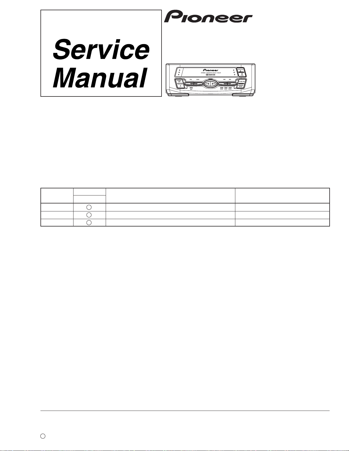
STEREO CASSETTE DECK
CT-IS21
THIS MANUAL IS APPLICABLE TO THE FOLLOWING MODEL(S) AND TYPE(S).
Type
MY AC220-230V
NV AC230V
RBD AC110-127V/220-240V With the voltage selector
Model
CT-IS21
Power Requirement
The Voltage can be converted by
the following method.
ORDER NO.
RRV2142
CONTENTS
1. SAFETY INFORMATION
2. EXPLODED VIEWS AND PARTS LIST
3. BLOCK DIAGRAM AND SCHEMATIC DIAGRAM..10
4. PCB CONNECTION DIAGRAM
5. PCB PARTS LIST
6. ADJUSTMENT
PIONEER ELECTRONIC CORPORATION 4-1, Meguro 1-Chome, Meguro-ku, Tokyo 153-8654, Japan
PIONEER ELECTRONICS SERVICE, INC. P.O. Box 1760, Long Beach, CA 90801-1760, U.S.A.
PIONEER ELECTRONIC (EUROPE) N.V. Haven 1087, Keetberglaan 1, 9120 Melsele, Belgium
PIONEER ELECTRONICS ASIACENTRE PTE. LTD. 253 Alexandra Road, #04-01, Singapore 159936
c
PIONEER ELECTRONIC CORPORATION 1999
...............................................
....................................................
......................................
................
..........................
18
24
27
2
3
7. GENERAL INFORMATION
7.1 DIAGNOSIS
7.1.1 POWER ON SEQUENCE
7.1.2 DISASSEMBLY
7.2 PARTS
7.2.1 IC
8. PANEL FACILITIES AND SPECIFICATIONS
............................................................
.................................................
......................................
.........................................................
T – IZM MAY 1999 Printed in Japan
................................
......................
....
31
31
31
32
33
33
34
Page 2
CT-IS21
1. SAFETY INFORMATION
This service manual is intended for qualified service technicians ; it is not meant for the casual do-ityourselfer. Qualified technicians have the necessary test equipment and tools, and have been trained
to properly and safely repair complex products such as those covered by this manual.
Improperly performed repairs can adversely affect the safety and reliability of the product and may
void the warranty. If you are not qualified to perform the repair of this product properly and safely, you
should not risk trying to do so and refer the repair to a qualified service technician.
WARNING
This product contains lead in solder and certain electrical parts contain chemicals which are known to the state of California to cause
cancer, birth defects or other reproductive harm.
Health & Safety Code Section 25249.6 – Proposition 65
NOTICE
(FOR CANADIAN MODEL ONLY)
Fuse symbols (fast operating fuse) and/or (slow operating fuse) on PCB indicate that replacement parts must
be of identical designation.
REMARQUE
(POUR MODÈLE CANADIEN SEULEMENT)
Les symboles de fusible (fusible de type rapide) et/ou (fusible de type lent) sur CCI indiquent que les pièces
de remplacement doivent avoir la même désignation.
(FOR USA MODEL ONLY)
1. SAFETY PRECAUTIONS
The following check should be performed for the
continued protection of the customer and service
technician.
LEAKAGE CURRENT CHECK
Measure leakage current to a known earth ground (water
pipe, conduit, etc.) by connecting a leakage current tester
such as Simpson Model 229-2 or equivalent between the
earth ground and all exposed metal parts of the appliance
(input/output terminals, screwheads, metal overlays, control
shaft, etc.). Plug the AC line cord of the appliance directly
into a 120V AC 60Hz outlet and turn the AC power switch
on. Any current measured must not exceed 0.5mA.
Reading should
not be above
0.5mA
Earth
ground
Device
under
test
Also test with
plug reversed
(Using AC adapter
plug as required)
Leakage
current
tester
Test all
exposed metal
surfaces
ANY MEASUREMENTS NOT WITHIN THE LIMITS
OUTLINED ABOVE ARE INDICATIVE OF A POTENTIAL
SHOCK HAZARD AND MUST BE CORRECTED BEFORE
RETURNING THE APPLIANCE TO THE CUSTOMER.
2. PRODUCT SAFETY NOTICE
Many electrical and mechanical parts in the appliance
have special safety related characteristics. These are
often not evident from visual inspection nor the protection
afforded by them necessarily can be obtained by using
replacement components rated for voltage, wattage, etc.
Replacement parts which have these special safety
characteristics are identified in this Service Manual.
Electrical components having such features are identified
by marking with a
in this Service Manual.
The use of a substitute replacement component which does
not have the same safety characteristics as the PIONEER
recommended replacement one, shown in the parts list in
this Service Manual, may create shock, fire, or other hazards.
Product Safety is continuously under review and new
instructions are issued from time to time. For the latest
information, always consult the current PIONEER Service
Manual. A subscription to, or additional copies of, PIONEER
Service Manual may be obtained at a nominal charge from
PIONEER.
on the schematics and on the parts list
AC Leakage Test
2
Page 3
2. EXPLODED VIEWS AND PARTS LIST
NOTES:• Parts marked by "NSP" are generally unavailable because they are not in our Master Spare Parts List.
2.1 PACKING
The mark found on some component parts indicates the importance of the safety factor of the part.
•
Therefore, when replacing, be sure to use parts of identical designation.
Screws adjacent to mark on the product are used for disassembly.
•
11
6
5
NV type only
12
CT-IS21
7 (MY type
only)
8 (MY ,NV
types only)
9 (RBD type
only)
10 (MY ,NV
types only)
1
(1) PACKING PARTS LIST
Mark No. Description Part No.
1 F Pad AHA7267
2 R Pad AHA7268
3 Packing Case See Contrast table (2)
4 Mirror Mat Sheet Z23-026
5 System Cable ADE7032
6 RCA Pin-plug Stereo Cable ADE7034
7 Operating Instructions See Contrast table (2)
(Spanish/Portuguese/Dutch/Swedish)
4
2
3
Mark No. Description Part No.
8 Operating Instructions See Contrast table (2)
(English/French/German/Italian)
9 Operating Instructions See Contrast table (2)
(English/Chinese/Spanish/Arabic)
NSP 10 Warranty Card See Contrast table (2)
11 Polyethylene Bag Z21-038
(0.03 × 230 × 340)
12 Protector V See Contrast table (2)
(2) CONTRAST TABLE
CT-IS21/MY, NV and RBD are constructed the same except for the following :
Mark No. Symbol and Description
3 Packing Case Y AHD7788 Not used Not used
3 Packing Case V Not used AHD7789 Not used
3 Packing Case D Not used Not used AHD7786
7 Operating Instructions ARC7265 Not used Not used
(Spanish/Portuguese/Dutch/Swedish)
8 Operating Instructions
9 Operating Instructions (English/Chinese/Spanish/Arabic) Not used Not used ARE7235
NSP 10 Warranty Card ARY7022 ARY7022 Not used
12 Protector V Not used AHA7273 Not used
(English/French/German/Italian) ARE7234 ARE7234 Not used
MY Type NV Type RBD Type
Part No.
Remarks
3
Page 4
CT-IS21
2.2 EXTERIOR
25
33
6
Refer to "2.3 and
2.4 DECK MECHANISM UNIT".
34
31
32
34
17
17
33
32
33
13
32
32
18
32
33
30
RBD
2
8
type
only
7
32
33
33
A
15
35
32
4
9
14
5
33
19
32
11
1
10
33
33
29
34
3
28(3/3)
33
33
24(1/2)
28(1/3)
12
22
A
27(2/2)
23
26(1/2)
26(2/2)
28(2/3)
21
27(1/2)
20
16
36
24(2/2)
4
Page 5
(1) EXTERIOR PARTS LIST
CT-IS21
Mark No. Description Part No.
1 AF Assy See Contrast table (2)
2 U-COM Assy AWU7370
3 DISPLAY Assy AWU7373
4 MAIN Assy See Contrast table (2)
5 REG. Assy AWU7369
6 Deck Mechanism Unit See Contrast table (2)
7 FU1 Fuse (T250mA) AEK1048
8 FU2 Fuse (T315mA) See Contrast table (2)
9 T2000 Power Transformer ATT7051
10 AC Power Cord See Contrast table (2)
11 Rear Panel See Contrast table (2)
12 Rubber Sheet AEB1111
13 Spacer AEB7133
14 Nylon Rivet AEC-525
15 Insulation Sheet AEC7208
NSP 16 Chassis MD, CD ANA7092
17 Mech Angle T ANG7213
18 Heat Sink IS ANH7111
Mark No. Description Part No.
19 Strain Relief CM-22B
20 Foot Assy REC-434
21 Function Button A AAD7510
22 Function Button B AAD7511
23 Play Button AAD7534
24 O/C Button AAD7535
25 Tray Cap AAK7678
26 Play Lens AAK7679
27 REC Lens AAK7680
28 Center Lens AAK7681
29 Front Panel AMB7640
30 Bonnet IS AZN7788
NSP 31 Tray Seal RRW1162
32 Screw BBZ30P060FMC
33 Screw BBZ30P080FZK
34 Screw BPZ30P080FMC
35 Binder ZCA-SKB90BK
36 Caution Label See Contrast table (2)
(2) CONTRAST TABLE
CT-IS21/MY, NV and RBD are constructed the same except for the following :
Mark No. Symbol and Description
1 AF Assy AWU7371 AWU7371 AWU7372
4 MAIN Assy AWU7365 AWU7365 AWU7366
6 Deck Mechanism Unit AXA7073 AXA7073 AXA7082
8 FU2 Fuse (T315mA) Not used Not used AEK1049
10 AC Power Cord HE PDG1003 Not used Not used
MY Type NV Type RBD Type
Part No.
Remarks
10 AC Power Cord HB Not used VDG1062 Not used
10 AC Power Cord SD Not used Not used PDG1013
11 Rear Panel Y ANC7857 Not used Not used
11 Rear Panel V Not used ANC7858 Not used
11 Rear Panel D Not used Not used ANC7853
36 Caution Label Not used Not used ARW7036
5
Page 6
CT-IS21
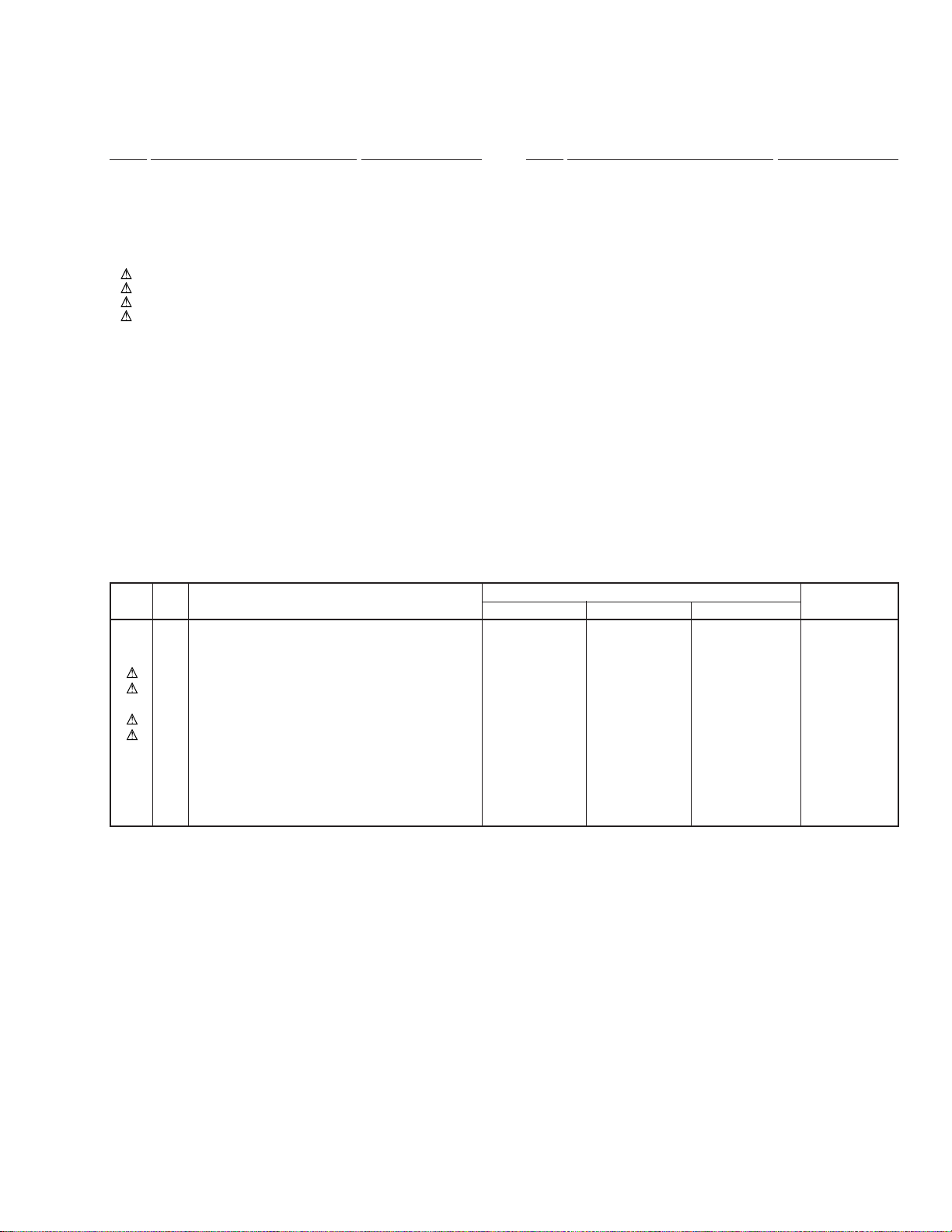
2.3 DECK MECHANISM UNIT (1/2)
17
4
16
6
5
16
19
16
12
13
14
3
1
11
9
4
16
10
20
20
16
18
8
7
20
21
2
2
Refer to "2.4. DECK MECHANISM UNIT (2/2).
6
Page 7

(1) DECK MECHANISM UNIT (1/2) PARTS LIST
Mark No. Description Part No.
1 Screw FG114-14
2 Screw UG12H-15
3 Front BKT FC64K-11
4 Washer MJ112-22
5 SP Return FK34N-11
6 Plate Hold BLK F573-258
7 Holder CST BLK F527-078
8 LDG Base FD56R-12
9 Pulley FD56T-11
10 LDG Gear FD56U-11
11 Slider FD57E-11
12 LDG Belt FF19L-12
13 Switch UE15S-14
14 MTR Reel BLK F564-313
15 • • • • •
16 Screw UG12H-28
17 SP Clamper FK34M-11
18 Switch UE18P-21
19 LUG UH12R-11
20 Earth Spring FK34S-11
CT-IS21
21 LUG UH12T-11
7
Page 8
CT-IS21
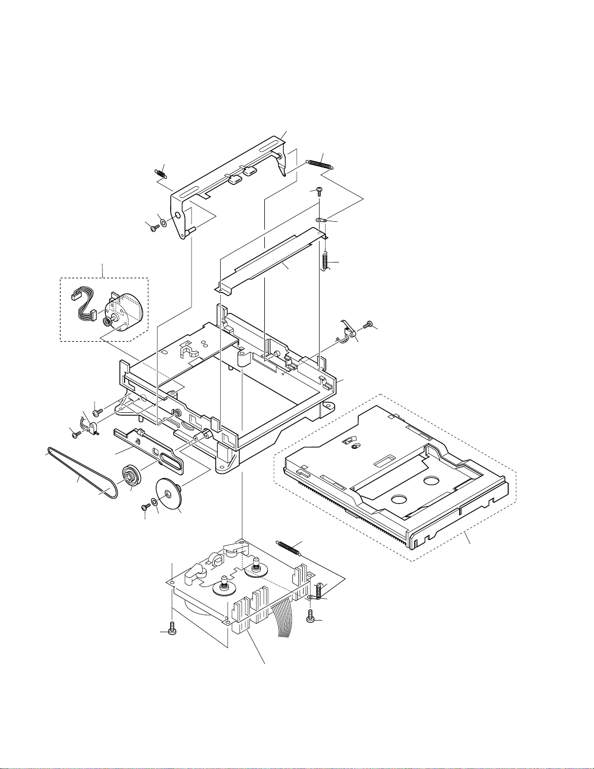
2.4 DECK MECHANISM UNIT (2/2)
39
40
19
33
15
12
31
10
4
2
32
2
8
23
5
14
31
32
7
9
3
18
34
11
6
16
24
21
43
35
37
36
30
13
20
30
41
42
27
22
26
9
17
28
1
29
1
3
25
38
8
Page 9

(1) DECK MECHANISM UNIT (2/2) PARTS LIST
CT-IS21
Mark No. Description Part No.
1 Screw KG194-36
2 Reel Feather FD57D-13
3 Screw UG11S-14
4 SP Reel(L) FK32U-12
5 SP Brake FK33B-13
6 SP Arm Play FK33P-11
7 SP Reel(R) FK32V-12
8 Spring Cassette FC65M-11
9 BKT MTR FC64M-12
10 Reel Base FD52W-12
11 Cam Gear FD52Y-23
12 Play Gear (A) FD53K-12
13 Arm Play FD53D-19
14 Plate Slide FC61L-19
15 PCB Control BLK F567-617
16 Chassis base BLK F612-231
17 Head Base FC61K-32
18 Roller Pinch BLK R F514-129
19 Roller Pinch BLK L F514-130
20 Assy F/W See Contrast table (2)
21 Clutch Assy BLK F522-037
22 Clutch Assy BLK See Contrast table (2)
Mark No. Description Part No.
23 Washer FJ111-13
24 F/R Pulley FD53F-15
25 Solenoid BLK F765-279
26 F/R Belt FF18W-12
27 Belt Main FF19H-11
28 Plate HD BLK F513-824
29 MTR MAIN BLK F525-327
30 Washer FJ111-30
31 Washer FJ111-35
32 Washer UJ16F-11
33 Lever Brake FD53P-17
34 FF Gear(A) FD53L-12
35 Cam SP FK32S-14
36 Screw UJ14A-12
37 Lever F/R FC62G-14
38 Plunger FL41S-21
39 Mecha-Cable WH65N-11
40 Spring HB FK32T-31
41 Screw UG15V-13
42 Washer MJ112-22
43 Spacer UJ15V-13
(2) CONTRAST TABLE
AXA7073 and AXA7082 are constructed the same except for the following :
Mark No. Symbol and Description
20 Assy F/W FR24S-11 FR24S-21
22 Clutch Assy BLK F522-042 F522-048
AXA7073 AXA7082
Part No.
Remarks
9
Page 10
1
23
CT-IS21
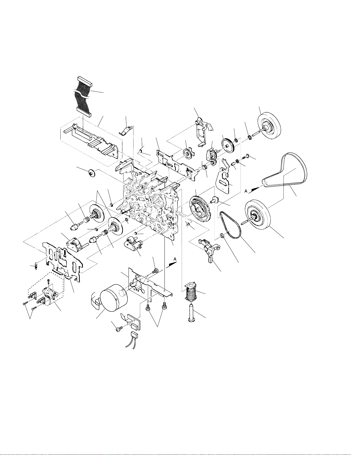
3. BLOCK DIAGRAM AND SCHEMATIC DIAGRAM
3.1 BLOCK DIAGRAM
4
A
REC/PB
HEAD
DECK
MECHANISM
B
UNIT
AXA7073
(MYandNV types)
AXA7082
(RDB type)
ERACE
HEAD
CN2302
CN2301
Lch
3
4
2
Rch
1
1
2
Vref
GNDA
Vref
L2801
RTD1082
6
4
5
VR2801
PCP1032
100K-B
OFFSET
VR2802
PCP1032
100K-B
2
1
3
BIAS
BIAS OSC
Q2801
2SC1815
Q2802
2SC1815
GNDB
GNDB
Q2301
Q2301
2SK373
2SK373
D
D
G
G
Q2302
2SK373
D
G
VB12
Q2803
2SB1238X
Q2804
DTC124EK
BIAS
Q2805
2SC1815
S
S
Q2351
DTA124EK
DTC124EK
S
IC2401(1/2)
BA4558F-HT
REC EQ
AMP
IC2401(2/2)
BA4558F-HT
Q2352
GNDA
7
8
1
4
Vref Vref
VA12
VA12
DTC114TK
GNDA
Q2353
DTC124EK
PB/REC
5
6
Vref Vref
3
2
Q2303
Q2304
DTC114TK
Q2401
DTC114TK
Q2402
DTC114TK
Vref
PB AMP
Vref
Q2451
2SD2114K
Vref
Vref
VA12
3
3
2
2
EQ
EQ
5
6
EQ
GNDA
Q2452
2SD2114K
IC2301(1/2)
IC2301(1/2)
BA4558F-HT
BA4558F-HT
8
8
1
1
4
4
GNDA
IC2301(2/2)
BA4558F-HT
7
VA12
Q2460
DTA124EK
Q2453
DTC124EK
Q2305
DTC114TK
Q2306
DTC114TK
VR2401
PCP1028
4.7K-B
VR2402
PCP1028
4.7K-B
VR2301
PCP1028
4.7K-B
PB LEVEL ADJ.
VR2302
PCP1028
4.7K-B
MTZ6.2A
Vref
REC LEVEL ADJ.
VA12
Q2454
DTA124EK
RECMUTE
Vref
Vref
D2201
GNDA
Vref
Vref
CRO2
PB/REC
BIAS
VR2701
RCP1024
C
13
12
11
10
9
8
7
6
5
4
3
2
1
13
12
11
10
9
8
7
6
5
4
3
2
1
1K-B
GNDM
MODE
VM12
2SB1425
GNDM
XMOTOR
Q2701
CrO2
HALF
F.REC
MODE
R.REC R.REC
CN2701
Q2752
DTA143EK
CN2751
D
1
2
3
4
5
5
1
4
2
3
3
2
4
1
5
TOUT
OPEN
CLOSE
Q2754
GNDM
GNDM GNDM
U-COM ASSY
AWU7370
VM12
Q2702
2SB1296
GNDM
VM12
LOADING
Q2753-2756
:2SD1858X
Q2756
Q2755
DTC124EK
GNDC
DTA124EK
Q2703
Q2704
SOL
GNDC
Q2753
VSS1045
MECHA
CONT
V+5
Q2751
DTA143EK
GNDM
X2501
6MHz
SENS
CrO2
HALF
F.REC
MODE
TOUT
TIN
OPEN
CLOSE
10
11
3
µ-COM
2
16
20
21
23
17
19
47
1
40
41
IC2501
PDC059A
32
30
28
26
4
15
46
45
43
44
22
39
37
33
25
14
13
35
36
34
32
Q2060
DTA124EK
Q2059
2SC2412K
RESET
Q2058
2SC2412K
V+5
Q2057
DTA114TK
CN2501
POW
AM56
SDATA
S.REQ
S.CLK
BIAS
XCrO2
PB/XREC
RECMUTE
SYSTEM ON
DOL ON/OFF
PB MUTE
LINE MUTE
V+5
GNDD
GNDM
VM12
RESET
CN2502
CN2601
KEY2
KEY1
LEDCE
LEDCLOCK
LEDDATA
POW
V+5
GNDD
1
2
3
4
5
MS
6
7
8
9
10
11
NC
12
13
14
15
1
2
3
4
5
1
2
3
4
5
6
7
8
10
1234
Page 11
5
678
CT-IS21
Note : When ordering service parts, be sure to refer to "EXPLODED VIEWS and PARTS LIST" or "PCB PARTS LIST".
3
14
4
8
9
CRO2
IC2201
HA12136AF
DOLBY-B NR
-3.7dBV
-3.7dBV
-32.2dBV
-32.2dBV
6
11
IC2202(1/2)
BA4558F-HT
ALC
2SC2412K
2SC2412K
Vref
5
LINEOUT BUFFER
TP
-6.0dBV
Q2261
2SD2114K
Vref
TP
-6.0dBV
Q2262
2SD2114K
Vref
VA12
3
8
1
2
4
GNDA
VA12
Q2253
Q2251
Q2252
2SC2412K
Vref
RTF1217
RTF1217
5
6
VA12
3
2
GNDA
F2201
MPX
F2202
MPX
MPX
IC2151(1/2)
BA4558F-HT
7
IC2151(2/2)
8
BA4558F-HT
1
4
5
6
IC2101(1/2)
BA4558F-HT
351
-8.0dBV
IC2101(2/2)
BA4558F-HT
3516
-8.0dBV
IC2202(2/2)
BA4558F-HT
AF ASSY
AWU7371(MY and NV types)
AWU7372(RBD type)
Q2171
2SD2114K
Vref
Q2172
2SD2114K
Vref
7
+
MS
VA12
3
8
1
2
4
GNDA
5
7
6
INPUT BUFFER
:PLAYBACK SIGNAL ROUTE
:RECRDING SIGNAL ROUTE
LINEOUT
Lch
GNDA
LINEOUT
Rch
GNDA
Q2263
DTC143EK
GNDA
GNDA
LINEIN
Lch
LINEIN
Rch
+
+
GNDD
CN2506
Q2173
DTA124EK
CN2505
VC5
15
14
MS
3
12
13
1 GNDB
5
6
11
8
V+B
LMUTE
PBMUTE NCNC
GNDA
GNDD
ON/OFF
CrO2
MS
NC
DOL
15
14
3
12
13
1
5
6
11
8
LINEMUTE
MS
DOL
ON/OFF
CrO2
A
B
PB/REC
RECMUTE
BIAS
CN2503
1
2
3
4
5
6
7
8
9
10
11
12
13
14
15
1
2
3
4
5
CN2504
J2601
1
1
2
2
3
3
4
4
5
5
6
6
7
7
8
8
POW
AM56
S.DATA
S.REQ
S.CLK
MS
BIAS
XCrO2
PB/XREC
RECMUTE
NC
NC
DOL ON/OFF
PB MUTE
LINE MUTE
V+5
GNDD
GNDM
VM12
RESET
KEY2
KEY1
LEDCE
LEDCLK
LEDDATA
POW
V+5
GNDD
CN2551
4
IC2502
3
BU2092F
2
DTC143EK
9 - 16
Q2601
23451
NC
AM56
SDATA
SCLOCK
REQ/ENA
MAIN ASSY
AWU7365(MY and NV types)
AWU7366(RBD type)
DISPLAY
ASSY
AWU7373
VB12
VA12
Q2051
GNDC
UN+5
GND
2SB1238X
VC5
UN+5
IC2057
NJM78M05FA
VC5
VC5
+5V
678
Q2061
2SC2412K
GNDC GNDM
M+12
MGND
AEK7011
AEK7011
AEK7011
UN12
M+12
Q2056
2SD2395
9
10
7
2
4
IC2051
1.5A
IC2052
1.5A
IC2053
1.5A
PB/REC
RECMUTE
BIAS
B+12
VA12
TRANSFORMER
UN12
IN OUTIN OUT
IC2055
NJM7812FA
PB/REC
9
RECMUTE
10
7
2
4
POWER
ATT7051
BIAS
+12V
FU1
T250mA
MY and NV
FU1
types
FU2
AEK1049
T315mA
AEK1048
GNDA GNDB
CN2051
23451678
GND
23451
J2052
REG.
ASSY
AWU7369
FU2
RDB
type
S2001
VOLTAGE
SELECTOR
AKX7004
C
NEUTRAL
LIVE
D
11
5
6
7
8
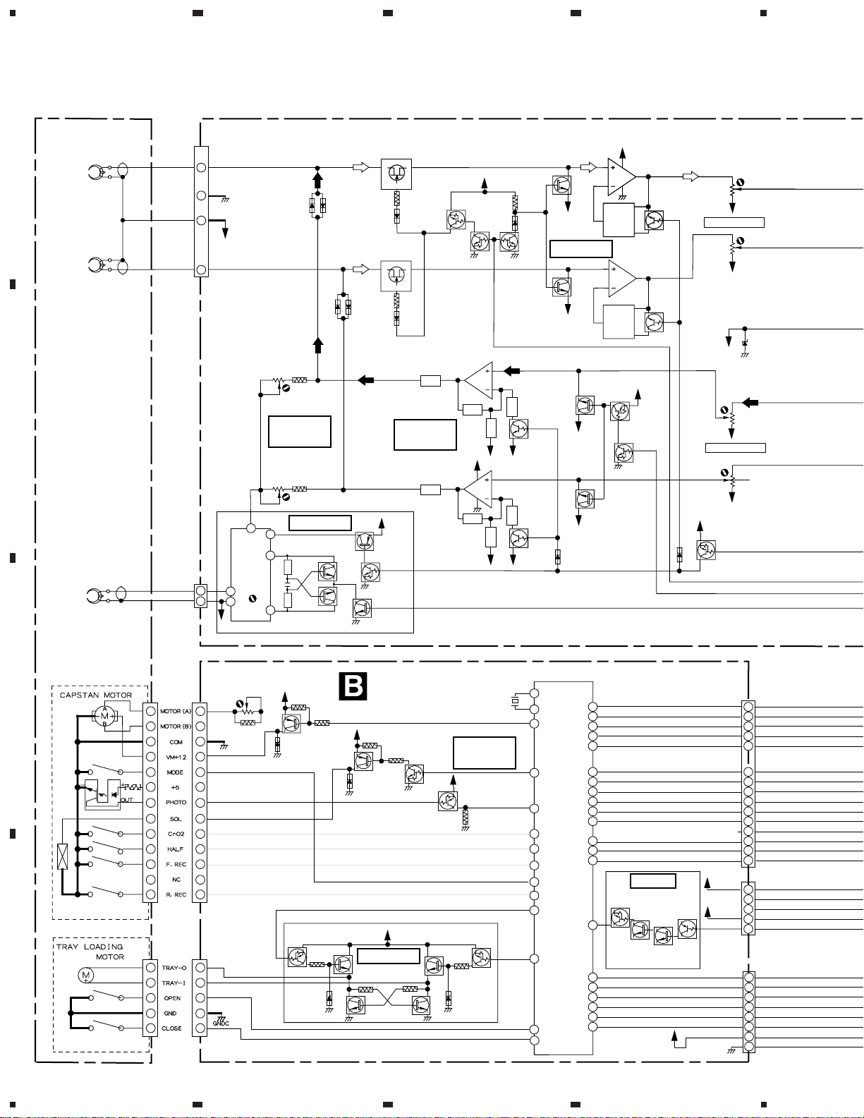
Page 12

CT-IS21
3.2 AF ASSY
A
B
DECK MECHA
UNIT (1/2)
(AXA7073
:MY, NV TYPES)
(AXA7082
:RBD TYPE)
1
REC/PB
HEAD
ERASE
HEAD
CN2301
CN2302
23
AF ASSY
A
(AWU7371: MY, NV TYPES)
(AWU7372: RBD TYPE)
D2301-D2306:
1SS133
C2315,
C2321-C2324
; MY and NV
types only
4
BA4558BF-HT
C
BA4558BF-HT
PCB BINDER
D
12
A
1234
NOTES
ALL CAPACITORS ARE IN µF
UNLESS OTHERWISE SPECIFIED.
ELECT.
Page 13

5
678
CT-IS21
MTZJ6.2A
D2252-D2255:
1SS355
: PLAYBACK SIGNAL ROUTE
: RECORDING SIGNAL ROUTE
A
B
BA4558BF-HT
BA4558BF-HT
ALL RESISTORS ARE IN Ω
UNLESS OTHERWISE SPECIFIED.
1/4W UNLESS OTHERWISE SPECIFIED
: CHIP (1/10W)
ALL INDUCTORS ARE IN µF.
: The power supply is shown
with the marked box.
5
CN2506
REC
CN2101(1/4)
CN2101(2/4)
6
PLAY
CN2101(3/4)
L
L
RR
CN2101(4/4)
CN2505
D
BA4558BF-HT
BA4558BF-HT
C
D
A
7
8
13
Page 14

1
CT-IS21
3.3 U-COM AND DISPLAY ASSYS
CN2701
A
DECK MECHA
UNIT (2/2)
(AXA7073
B
:MY, NV TYPES)
(AXA7082
:RBD TYPE)
23
4
CN2751
U-COM ASSY
B
C
D2602,D2603,
D2605-D2609:
(AWU7370)
C
DISPLAY ASSY
(AWU7373)
PCB BINDER
CN2601
CABLE
HOLDER
J2601
LED DRIVER
D
PCB BINDER
14
B
C
1234
Page 15

5
678
CT-IS21
A
MTZJ6.8C
B
CN2502
CN2504
D
S2901-S2904,S2906-S2912:
ASG7013
CN2501
1SS133
CN2503
D
SWITCHES
DISPLAY ASSY
S2901 : STANDBY/ON
S2902 : ASEB
S2903 : 2
S2904 : 3
S2906 : OPEN CLOSE (0)
S2907 : ¶8
S2908 : 1
S2909 : ¡
S2910 : STOP (7)
S2911 : REVERSE MODE
S2912 : DOLBY NR
RESET
NOTES
ALL CAPACITORS ARE IN µF
UNLESS OTHERWISE SPECIFIED.
ELECT.
ALL RESISTORS ARE IN Ω
UNLESS OTHERWISE SPECIFIED.
: CHIP (1/10W)
: The power supply is shown
with the marked box.
C
D
B
5
6
7
C
8
15
Page 16

1
CT-IS21
3.4 MAIN AND REG. ASSYS
AC POWER CORD
A
PDG1003 (MY TYPE)
VDG1062 (NV TYPE)
PDG1013 (RBD TYPE)
CN2001
AC IN
AWU7366
ONLY
FU1 250mA/250V
AEK1048
23
4
S2001
VOLTAGE
SELECTOR
AKX7004
B
AC220-240V
AC110-127V
FU2 315mA/250V
AEK1049
AWU7365
ONLY
T2000
POWER TRANSFORMER
ATT7051
SCREW
TERMINAL
CN2551
D
MAIN ASSY
(AWU7365: MY, NV TYPES)
(AWU7366: RBD TYPE)
SYSTEM
C
D
16
D
1234
CN2505
CN2506
A
Page 17

5
678
CT-IS21
A
REGULATOR
CN2051
PCB BINDER
J2052
CABLE HOLDER
E
REGULATOR
REG. ASSY
(AWU7369)
B
CN2501
B
C
CN2503
NOTES
ALL CAPACITORS ARE IN µF
UNLESS OTHERWISE SPECIFIED.
ELECT.
ALL RESISTORS ARE IN Ω
UNLESS OTHERWISE SPECIFIED.
1/4W UNLESS OTHERWISE SPECIFIED
: CHIP (1/10W)
• NOTE FOR FUSE REPLACEMENT
CAUTION -
5
FOR CONTINUED PROTECTION AGAINST RISK OF FIRE.
REPLACE WITH SAME TYPE AND RATINGS ONLY.
CN2502
B
CN2504
D
D
6
7
E
8
17
Page 18

1
2
23
CT-IS21
4. PCB CONNECTION DIAGRAM
4.1 AF ASSY
A
SIDE A
A
B
4
AF ASSY
NOTE FOR PCB DIAGRAMS :
1. Part numbers in PCB diagrams match those
in the schematic diagrams.
2. A comparison between the main parts of PCB
and schematic diagrams is shown below.
Symbol In PCB
Diagrams
BCE
C
D
3. The parts mounted on this PCB include all
necessary parts for several destinations.
For further information for respective destinations,
be sure to check with the schematic diagram.
4. View point of PCB diagrams.
Connector
BCE
Symbol In Schematic
Diagrams
BCEBCE
BCE
BCE
DGS
DGGSS
Capacitor
Part Name
Transistor
Transistor
with resistor
Field effect
transistor
Resistor array
3-terminal
regulator
SIDE A
SIDE B
AF ASSY
A
CN2505
D
P.C.Board
D
18
A
Chip Part
1234
SIDE B
Q2171
Q2172
IC2151
IC2101
Q2261Q2263Q2173
Q2262
IC2202
Q2252
Q2251
Q2254
Q2253
Q2255
IC
Page 19

5
Q
678
CT-IS21
VR2301
VR2302
VR2401
VR2402
(ANP7329-B)
Q2301 Q2801
Q2805Q2302
Q2802
Q2803
VR2801
VR2802
REC/PB
HEAD
A
B
ERASE
HEAD
2254
Q2253 IC2201
Q2460
Q2453
Q2353 Q2351
Q2305
Q2402Q2452
Q2401Q2451
IC2301
IC2401
DECK MECHA UNIT
Q2456
Q2455Q2303
Q2804Q2304Q2306Q2352Q2454Q2255
(ANP7329-B)
C
D
5
6
7
A
8
19
Page 20

1
23
CT-IS21
4.2 U-COM AND DISPLAY ASSYS
4
A
DISPLAY ASSY
C
CAPSTAN
MOTOR
DECK
MECHA
UNIT
B
TRAY
LOADING
MOTOR
U-COM ASSY
B
VR2701
D
CN2503
Q2701
Q2702
Q2753
Q2754
Q2755
Q2756
D
CN2504
C
D
(ANP7329-B)
(ANP7329-B)
SIDE A
20
B C
1234
Page 21

1
U-COM ASSY
B
234
CT-IS21
DISPLAY ASSY
C
A
Q2703
Q2752
Q2751
Q2704
Q2057
Q2058
Q2059
Q2060
Q2561
IC2502
B
Q2601
C
IC2501
Q2563
Q2564
Q2562
D
(ANP7329-B)
(ANP7329-B)
SIDE B
B
1
2
3
C
4
21
Page 22

1
23
CT-IS21
4.3.MAIN AND REG. ASSYS
4
B
CN2502
A
MAIN ASSY
D
AC IN
NEUTRAL
B
REG. ASSY
E
LIVE
B
CN2501
IC2051
IC2052
IC2053
C
IC1
IC2054
Q2051
D
(ANP7329-B)
A
CN2506
(ANP7329-B)
SIDE A
22
D E
1234
Page 23

1
MAIN ASSY
D
234
CT-IS21
A
B
Q2061
REG. ASSY
E
C
Q2052
(ANP7329-B)
(ANP7329-B)
D
SIDE B
D E
1
2
3
4
23
Page 24

CT-IS21
Mark No. Description Part No.
Mark No. Description Part No.
5. PCB PARTS LIST
NOTES:•Parts marked by "NSP" are generally unavailable because they are not in our Master Spare Parts List.
The mark found on some component parts indicates the importance of the safety factor of the part.
•
Therefore, when replacing, be sure to use parts of identical designation.
When ordering resistors, first convert resistance values into code form as shown in the following examples.
•
Ex.1 When there are 2 effective digits (any digit apart from 0), such as 560 ohm and 47k ohm (tolerance is shown by J=5%,
and K=10%).
560 Ω→56 × 10
47k Ω→47 × 103→ 473 ........................................................ RD1/4PU 4 7 3 J
0.5 Ω→R50 ..................................................................................... RN2H
1 Ω→1R0 ..................................................................................... RS1P
Ex.2 When there are 3 effective digits (such as in high precision metal film resistors).
5.62k Ω→ 562 × 10
LIST OF HOLE PCB ASSEMBLIES
Mark Symbol and Description
NSP COMPLEX ASSY
AF ASSY
U-COM ASSY
DISPLAY ASSY
MAIN ASSY
REG. ASSY
1
→ 561 ........................................................ RD1/4PU 5 6 1 J
R 5 0
1 R 0
1
→ 5621 ...................................................... RN1/4PC 5 6 2 1 F
Part No.
CT-IS21/MY CT-IS21/NV CT-IS21/RBD
AWM7463
AWU7371
AWU7370
AWU7373
AWU7365
AWU7369
AWM7463
AWU7371
AWU7370
AWU7373
AWU7365
AWU7369
AWM7464
AWU7372
AWU7370
AWU7373
AWU7366
AWU7369
K
K
Remarks
PCB PARTS LIST
Mark No. Description Part No.
AF ASSY
A
(1) CONTRAST TABLE
AWU7371 and AWU7372 are constructed the same except
for the following :
Mark Symbol and Description
C2323,C2324 CCSQCH100D50 Not used
C2321,C2322 CCSQCH470J50 Not used
C2315 CKSQYB102K50 Not used
AWU7371 AWU7372
(2) PARTS LIST FOR AWU7371
SEMICONDUCTORS
IC2101,IC2151,IC2202 BA4558F-HT
IC2301,IC2401 BA4558F-HT
IC2201 HA12136AF
Q2254 2SA1037K
Q2803 2SB1238X
Q2801,Q2802,Q2805 2SC1815
Q2251-Q2253 2SC2412K
Q2171,Q2172,Q2261,Q2262 2SD2114K
Q2451,Q2452 2SD2114K
Q2301,Q2302 2SK373
Q2173,Q2351,Q2454,Q2460 DTA124EK
Q2303-Q2306,Q2401,Q2402 DTC114TK
Q2255,Q2352,Q2353,Q2453,Q2804
Q2263 DTC143EK
D2256,D2301-D2306 1SS133
D2252-D2255,D2307,D2308,D2401
D2201 MTZJ6.2A
Part No.
Remarks
DTC124EK
1SS355
Mark No. Description Part No.
COILS AND FILTERS
L2802 LFA121J
L2801 OSC COIL RTD1082
L2401,L2402 COIL 10mH RTF1004
L2403,L2404 COIL 4.7mH RTF1021
F2201,F2202 MPX FILTER RTF1217
CAPACITORS
C2301,C2302,C2323,C2324 CCSQCH100D50
C2423,C2424 CCSQCH221J50
C2253 CCSQCH271J50
C2321,C2322 CCSQCH470J50
C2153,C2154,C2203,C2207 CEAT100M50
C2215 CEAT101M16
C2251 CEAT220M50
C2216 CEAT221M16
C2254 CEAT2R2M50
C2407 CEAT330M50
C2107,C2161,C2425 CEAT470M16
C2221,C2222,C2261,C2262 CEAT4R7M50
C2204,C2311,C2312 CEJA100M16
C2103,C2104,C2201,C2202
C2217,C2218,C2255,C2403,C2404
C2419,C2420 CEJA1R0M50
C2309,C2310,C2408,C2805,C2806
C2314,C2807 CEJA470M16
C2208 CEJAR10M50
C2205,C2206 CEJAR22M50
C2151,C2152,C2315 CKSQYB102K50
C2431,C2432 CKSQYB122K50
C2211,C2212 CKSQYB152K50
C2303,C2304 CKSQYB681K50
C2108 CKSQYF104Z50
CEJA1R0M50
CEJA1R0M50
CEJA330M16
24
Page 25

CT-IS21
Mark No. Description Part No.
C2252 CKSQYF105Z16
C2808 CQHA822J2A
C2209,C2210 CQMA103J50
C2801 CQMA123J50
C2421,C2422 CQMA152J50
C2409,C2410 CQMA223J50
C2417,C2418 CQMA393J50
C2803,C2804 CQMA472J50
C2307,C2308,C2802 CQMA682J50
C2405,C2406 CQMA683J50
RESISTORS
R2805 RD1/2VM161J
R2806 RD1/2VM201J
R2803 RD1/2VM4R7J
VR2301,VR2302,VR2401,VR2402 PCP1028
(4.7kΩ)
VR2801,VR2802 (100kΩ) PCP1032
Other Resistors RS1/10S J
OTHERS
CN2101 PIN JACK(4P) AKB7015
CN2302 KR CONNECTOR 2P B2B-PH-K-S
CN2301 KR CONNECTOR 4P B4B-PH-K-S
CN2506 15P SOCKET KP200TA15L
PCB BINDER VEF1040
U-COM ASSY
B
SEMICONDUCTORS
IC2501 PDC059A
Q2702 2SB1296
Q2701 2SB1425
Q2058,Q2059 2SC2412K
Q2753-Q2756 2SD1858X
Mark No. Description Part No.
OTHERS
CN2601 8
CN2701 KR CONNECTOR 13P B13B-PH-K-S
CN2751 KR CONNECTOR 5P B5B-PH-K-S
CN2501 15P SOCKET KP200TA15L
CN2502 5P SOCKET KP200TA5L
PCB BINDER VEF1040
X2501 CERAMIC RESONATOR VSS1045
(6.00MHz)
DISPLAY ASSY
C
P JUMPER CONNECTOR
52151-0810
SEMICONDUCTORS
IC2502 BU2092F
Q2601 DTC143EK
D2602,D2603,D2605-D2609 SLP3118C51H
D2601,D2604 SLP9118C51H
SWITCHES
S2901-S2904,S2906-S2912 ASG7013
CAPACITORS
C2601 CKSQYB102K50
C2604 CKSQYF104Z25
RESISTORS
All Resistors RS1/10S J
OTHERS
8P CABLE HOLDER 51048-0800
J2601 JUMPER WIRE 8P D20PYY0825G
PCB BINDER VEF1040
Q2057 DTA114TK
Q2060,Q2704 DTA124EK
Q2751,Q2752 DTA143EK
Q2562,Q2563 DTC114TK
Q2561 DTC115TK
Q2564,Q2703 DTC124EK
D2062 1SS133
D2751,D2752 MTZJ5.6C
D2501 MTZJ6.8C
D2701,D2702 S5688G
COIL
L2501 LAU220J
CAPACITORS
C2561,C2562 CCSQCH101J50
C2703 CEAT221M16
C2066 CEJA220M25
C2502 CEJA470M16
C2501,C2503,C2504,C2506-C2510
C2563,C2702,C2751 CKSQYB103K50
C2505 CKSQYB471K50
RESISTORS
R2751-R2754 RD1/4PU391J
R2708 RD1/4PU751J
VR2701 (1kΩ) PCP1024
Other Resistors RS1/10S J
CKSQYB103K50
MAIN ASSY
D
(1) CONTRAST TABLE
AWU7365 and AWU7366 are constructed the same except
for the following :
Mark Symbol and Description
H2001,H2002 Fuse Clip Not used AKR1003
S2001 Voltage Selector Not used AKX7004
Part No.
AWU7365 AWU7366
Remarks
(2) PARTS LIST FOR AWU7365
SEMICONDUCTORS
IC2051-IC2053
Q2051 2SB1238X
Q2061 2SC2412K
D2066,D2068 MTZJ15C
D2067 MTZJ6.8C
D2051-D2054,D2056,D2057 S5688G
PROTECTOR (1.5A)
AEK7011
CAPACITORS
C2555-C2558 CCSQCH101J50
C2065 CEAT100M50
C2058-C2060 CEAT331M16
C2052 CEAT332M25
C2051 CEAT332M35
RESISTORS
All Resistors RS1/10S J
25
Page 26

CT-IS21
Mark No. Description Part No.
OTHERS
CN2051
CN2551 5P SOCKET AKP7042
H2003,H2004 FUSE CLIP AKR1003
CN2503,CN2505 15P PLUG KM200TA15
CN2504 5P PLUG KM200TA5
TERMINAL RKC-061
PCB BINDER VEF1040
SCREW PLATE VNE1948
REG. ASSY
E
8P JUMPER CONNECTOR
52147-0810
SEMICONDUCTORS
IC2055 NJM7812FA
IC2057 NJM78M05FA
Q2056 2SD2395
CAPACITORS
C2049,C2054 CEJA1R0M50
RESISTORS
All Resistors RS1/10S J
OTHERS
8P CABLE HOLDER 51048-0800
J2052 JUMPER WIRE 8P D20PYY0810G
Mark No. Description Part No.
26
Page 27

6. ADJUSTMENT
6.1 TEST MODE
CT-IS21
How to Enter the Test Mode
Receive "A15F" (Bus code 1C5F) with the remote control unit or
plug the power cord into the AC socket with the TEST MODE JP
(W101 and W102) on the U-COM Assy short-circuited.
TEST MODE
Short point
W102
W101
Front
U-COM ASSY
SIDE A
3. When pressing the ASES key, the Auto-recording/playback
operation mode is reached and perform the following operation.
1 Function is set to AUX.
2 FWD recording is performed for 4 seconds.
3 REV recording is performed for 4 seconds.
4 FWD playback is performed for 4 seconds. (Function becomes
TAPE).
5 Stop
4. The same operation as before can be performed with the key except
for the REVERSE MODE and ASES keys.
However, the REVERSE mode should endless fix for ageing.
LINE MUTE (PB MUTE) is opened in the REC pause and
recording status.
Cancellation of the Test Mode
Press the "STANDBY/ON" key or disconnect the AC power cord.
About the Mechanism Ageing Mode
When pressing the ASES and STOP keys for 3 seconds in the wall
outlet on, Deck power is on and the ageing mode is reached.
PLAY indicator starts flashing when enter the ageing mode.
Fig. 6-1 Test mode
Operation of the Test Mode
1. LED check mode
When pressing the REVERSE MODE key, LED indication
changes as follows.
→ Normal display → All LED lights → All LED lights out
∗ STANDBY LED is not able to controlled with the microcomputer
because of it's lighted with the hardware.
2. When pressing the EJECT key, the Cassette mecha. SW check
mode is reached and LED displays as follows.
LED
DIR FWD
DIR REV
PLAY
REC
SW ON OFF
FWD REC SW
REV REC SW
HALF SW
TAPE TYPE
Enable the FWD
recording
Enable the REV
recording
Tape exist
NORMAL
Disenable the FWD
recording
Disnable the REV
recording
No Tape
CrO
2
6.2 ADJUSTMENT
Adjustment Condition
(1) Clean the heads and demagnetize them using a head eraser.
(2) Set the measurement level to 0 dBV = 1 Vrms.
(3) Use the specified tape for adjustment. Use the labeled (A) side
of the test tape.
NCT–111 : For Tape Speed Adjustment
: For Head Azimuth Adjustment
STD-331E : For Playback Level Adjustment
: For Playback Frequency Adjustment
STD–632 : Normal blank tape
STD–622 : CrO
(4) Provide yourself with the following measuring devides:
• AC millivoltmeter
• Low-frequency oscillator
• Attenuator
• Oscilloscope
(5) Adjust both right and left channels unless otherwise specified.
(6) Turn the DOLBY NR switch off unless otherwize specified.
(7) Warm up the unit for several minutes before adjustment. In
particular, be sure to warm up the unit in the REC/PLAY mode
for 3 to 5 minutes before starting recording/playback frequency
characteristics adjustment.
(8) Always follow the indicated adjustment order.
Otherwise, a complete adjustment may not be achieved.
2 blank tape
27
Page 28

CT-IS21
List of Adjustment
¶ Playback Section
(1) Tape Speed Adjustment
(2) Head Azimuth Adjustment
(3) Playback Level Adjustment
(4) Playback Frequency Characteristics Confirmation
¶ Recording Section
(1) Recording Bias Adjustment
(2) Recording Level Adjustment
(3) Recording Frequency Characteristics Confirmation
Dolby noise reduction manufactured under license from Dolby
Laboratories Licensing Corporation.
“DOLBY” and the double-D symbol are trademarks of Dolby
Laboratories Licensing Corporation.
0 dB
30s
315 Hz
0 dB: 315 Hz, 250 nwb/m
30 s 30 s 30 s 10s 10s .......................................................................................................... 10s
6.3 kHz 10 kHz 315 Hz 14 kHz
12.5
kHz
PLAY BACK
RECORDING
10 kHz
8 kHz 4 kHz2 kHz
250
3dB
250
3dB
Fig. 6-2 Frequency Characteristics
6.3
kHz
1 kHz
500Hz250Hz125
10k
3dB 4dB
10k
3dB
Hz
12.5k
12.5k
5dB
–20 dB
63 Hz 40 Hz
Fig. 6-3 Test Tape STD-331E
6.2.1 Playback Section
(1) Tape Speed Adjustment
No. Mode Input Signal/Test Tape Adjustment Points Measurement Points Adjustment Value Remarks
PLAY1
NCT-111 (3 kHz)
VR2701 (AF Assy)
(Refer to Fig. 6-4)
LINE OUT
(L, R ch)
(AF Assy)
(2) Head Azimuth Adjustment
• This unit is equipped with auto tape selector.
• Do not switch between forward and reverse operation with the screwdriver inserted.
No. Mode Input Signal/Test Tape Adjustment Points
PLAY1
STD-331E
(10 kHz, –20dB)
Head azimuth
adjustment Screw
(Fig. 6-4)
Measurement
Points
LINE OUT
(L, R ch)
(AF Assy)
3000 Hz ±10Hz
Adjustment
Value
Max. Playback
signal level
FWD adjustment
REV Confirmation
( 3000 Hz ± 40Hz )
Remarks
After adjustment, apply silicon
bond to the head azimuth
adjustment screw.
28
Page 29

(3) Playback Level Adjustment
• Since this adjustment determines playback DolbyNR level, Perform it carefully.
Measurement
Points
Adjustment
Value
CT-IS21
RemarksNo. Mode Input Signal/Test Tape Adjustment Points
PLAY1
STD-331E test tape
(Playback: 315 Hz, 0 dB)
L ch
R ch VR2302
VR2301
LINE OUT
(L, R ch)
(AF Assy)
–6.0 dBV
(4) Playback Frequency Characteristics Confirmation
Measurement
Points
PLAY1
STD-331E test tape
LINE OUT
(L, R ch)
(AF Assy)
Adjustment
Value
Check that the frequency
characteristics is within the
range of Fig. 6-2.
6.2.2 Recording Section
(1) Recording Bias Adjustment
• After the adjustment, caution should be exercised so as not to become under bias by checking the distortion rate.
No. Mode Input Signal/Test Tape Adjustment Points
REC/
1
PAUSE
REC =
2
PLAY
Input a 315Hz (–26 dBV) signal to
the LINE INPUT.
Load the STD–632 test tape and
record/playback the 315Hz and
10kHz signals. (see the Note below)
L ch
R ch VR2802
VR2801
Measurement
Points
LINE OUT
(L, R ch)
(AF Assy)
Adjustment
Value
–26 dBV
Repeat adjustment until playback level of
the 10kHz signal is within 0dB ± 0.5dB
from that of the 315Hz signal.
RemarksNo. Mode Input Signal/Test Tape Adjustment Points
Remarks
Note: Set the 10kHz input signal level to the same value as the 315Hz input signal level of step 1.
(2) Recording Level Adjustment
No. Mode Input Signal/Test Tape Adjustment Points
REC/
1
PAUSE
REC =
2
PLAY
Input a 315Hz signal to the LINE
INPUT.
• STD–632 test tape and record/
playback the 315Hz signal.
• DOLBY NR : OFF
Input signal level
L ch
R ch VR2402
VR2401
Measurement
Points
LINE OUT
(L, R ch)
(AF Assy)
(3) Recording Frequency Characteristics Confirmation
No. Mode Input Signal/Test Tape Adjustment Points
REC =
1
PLAY
• STD–632, STD-622 test tape
• Record with –26.0 dBV
• DOLBY NR : ON/OFF
Note : Impedance of LINE IN/OUT are as follows :
• LINE IN : 53 kΩ
• LINE OUT : 2 kΩ
Measurement
Points
LINE OUT
(L, R ch)
(AF Assy)
Adjustment
Value
Remarks
–10 dBV
Repeat recording, playback and
adjustment until playback level of the
315Hz signal becomes –
Adjustment
Value
Check that the frequency
characteristics is within the
range of Fig. 6-2.
10dBV ± 0.5dB
Remarks
.
29
Page 30

CT-IS21
Front
W102
W101
TEST MODE
Jumper
MECHANISM UNIT
U-COM ASSY
SIDE A
TAPE SPEED
VR2701
FWD Azimuth
Adjustment Screw
Front
REV Azimuth
Adjustment Screw
AF ASSY
PB LEVEL
VR2302
(R ch)
SIDE A
VR2301
(L ch)
VR2402
(R ch)
REC LEVEL
BIAS LEVEL
VR2802
(R ch)
VR2401
(L ch)
VR2801
(L ch)
30
Fig. 6-4 Adjustment and Measuring Points
Front
Page 31

7. GENERAL INFORMATION
7.1 DIAGNOSIS
7.1.1 POWER ON SEQUENCE
• STANDBY/ON key is pressed.
• Receive the system power on
information with the sytem bus.
Go to Power ON
CT-IS21
Note : Pin No. shows the Pin No. of µ-COM PDC059A.
Perform the mechanism initialization every time it power on.
(When the AC outlet is pulled out
while raising up the Head Base or
the gear comes off, perform the
initialization every time because the
normal movement can't be done.)
No
Is Tray open ?
Yes
Tray close
200mS WAIT
Is MODE SW
OFF ?
No
SOL 50mS ON
MOTOR ON
150mS WAIT
Yes
(port Pin 2 )
(port Pin 3 )
Check the mecha. switch (port Pin 40 and Pin 41 )
CLOSE Pin 40 = H , Pin 41 = L
OPEN Pin 40 = L , Pin 41 = H
Close it if the tray is opened (port Pin 1 and Pin 47 )
CLOSE Pin 1 = L , Pin 47 = H
OPEN Pin 1 = H , Pin 47 = L
Check that the mecha. is stop
condition (port Pin 17 = L)
MOTOR ON
500mS WAIT
No
Is MODE SW
OFF ?
No
Is it fifth
times ?
No
Is MODE SW
OFF ?
Yes
300mS WAIT
MOTOR OFF
END
Yes
:ERROR
(port Pin 3 )
Yes
ERROR
Is it second
times ?
Yes
:Give up
Initialize end
Deck motor off
(port Pin 3 = L)
No
31
Page 32

CT-IS21
7.1.2 DISASSEMBLY
FRONT PANEL
3
Bonnet IS
MAIN ASSY
1
×3
MAIN Assy
7
CN2051
3
×4
U-COM Assy
1
×4
9
4
6
AF Assy
2
About
30°
2
Deck Mechanism
Unit
REG. Assy
8
CN2302
5
AF Assy
CN2601
Unhook
CN2301
Rear Panel IS
MAIN Assy
(SIDE B)
10
4
6
AF Assy
8
5
×2
7
Unhook
Note : These screws are loosened.
Connect the above connectors.
Then, diagnose the MAIN Assy.
32
Page 33

CT-IS21
No. Pin Name I/O Pin Function No. Pin Name I/O Pin Function
1 TIN O Loader mechanism motor close 25 POFF I AC input detection
2 SOL O Solenoid control 26 S.R/E I/O System bus request
3 XMOTOR O Cassette mechanism motor control 27 S.DOUT O System bus output data
4 S.CLK I System bus clock 28 S.DIN I System bus input data
5 XRESET I Reset input 29 NC − Not used
6 E+5V I Connect to VDD 30 AM56 I System 5.6 input
7NC − Not used 31 XTEST I Test mode detection input
8 E+5V I Connect to VDD 32 POWER O Power control
9 GNDD − GND 33 LINEMUTE O Line mute control
10 6MHz I
Connect a crystal resonator
34 LEDDATA O IC DATA output for LED control
11 6MHz O 35 LEDCE O IC OK output for LED control
12 E+5V − Power supply +5V 36 LEDCLK O IC output for LED control
13 KEY1 I
AD key data input
37 PB MUTE O CLK (Not used)
14 KEY2 I 38 MODEL I Model switch input
15 MS I MS audio signal input 39 DOLBY O DOLBY NR control
16 SENSE I Sensing pulse input 40 XOPEN I Loader mechanism open SW control
17 XMODE I Cassette mechanism mode SW input 41 XCLOSE I Loader mechanism close SW input
18 NC − Not used 42 NC − Not used
19 XRECR I REV REC detection SW input 43 PB/XREC O DOLBY PB/REC control
20 XCrO
2
(SW) I CrO2 position detection SW input 44 RECMUTE O REC MUTE control
21 XHALF I Tape detection SW input 45 XCrO
2
O Normal / CrO2 control
22 NC 0 Non connection 46 BIAS O BIAS control
23 XRECF I FWD REC detection SW 47 TOUT O Loader mechanism motor open
24 NC − Not used 48 NC − Not used
7.2 PARTS
7.2.1 IC
• The information shown in the list is basic information and may not correspond exactly to that shown in the schematic diagrams.
PDC059A (U-COM ASSY : IC2501)
• System Microcomputer
Pin Function
•
33
Page 34

CT-IS21
8. PANEL FACILITIES AND SPECIFICATIONS
PANEL FACILITIES
34
Page 35

Accessories
System Cable ×1
(ADE7032)
RCA Pin-plug Stereo Cable ×2
(ADE7034) (L=50 cm)
White
Red
1 STANDBY/ON button and standby indicator
This is the power switch.
ON : When set to the ON position, power is supplied and the
STANDBY : When set to the STANDBY position, the main power flow
unit becomes operational.
is cut and the unit is no longer fully operational. A min ute
flow of power feeds the unit to maintain operation readiness.
Energy-Saving Design
This product has been designed to reduce energy consumption when the unit is in the power off (standby)
mode.
¶ Consult the Specifications for the power consumption
in standby mode.
NOTE:
When the Stereo Cassette Deck CT-IS21 is connected to
the XC-IS21MD or XC-IS21T via the system cable, the unit’ s
power will be switched on/off (standby) automatically by
operating the ST ANDBY/ON b utton of either of the connected
units.
2 Recording-pause button (¶8)
3 REC (recording) indicator
4 ASES button
5 Play indicator
6
Play buttons and direction indicators
(2, 3)
7 Reverse mode indicators
8 Fast forward/re ver se b uttons( 1, ¡)
9 Cassette tray
0 OPEN/CLOSE button (0)
- STOP button(7)
= DOLBY* NR button and indicator
*
Dolby noise reduction manufactured under license from
Dolby Laboratories Licensing Corporation.
“DOLBY” and the double-D symbol are trademarks of
Dolby Laboratories Licensing Corporation.
~ REVERSE MODE button
CT-IS21
SPECIFICATIONS
System ......................................................4-track, 2-channel stereo
Heads.................................................................... “Har d Permalloy”
recording/playback head × 1
“Ferrite” erasing head × 1
Motor ................................................................ DC servo motor × 2
Wow and Flutter........................................................*0.1% (WRMS)
Frequency Response
–20 dB recording:
TYPE II (High/CrO2) tape.............. *35 Hz to 15,000 Hz ±4 dB
TYPE I (Normal) tape ...................*35 Hz to 14,000 Hz ±4 dB
Signal-to-Noise Ratio
Dolby NR OFF............................................................. *55 dB
(peak recording level, audible compensation TYPE II)
Noise Reduction Effect
Dolby NR ON .......................... 10 dB compensation at 5 kHz
Input (Sensitivity)
REC ...................................100 mV (Input impedance 53 kΩ)
Output (Reference lev el)
PLAY ..................................... 0.5 V (Output impedance 2 kΩ)
Pow er Requirements
NV type ............................................................. AC 230 V, 50/60 Hz
MY type ................................................... AC 220 ~ 230 V, 50/60 Hz
RBD type ................................................ AC 110 ~ 127/220 ~ 240 V
(switchable), 50/60 Hz
Power Consumption ................................................................ 12 W
Power Consumption in standby mode........................................ 3 W
Dimensions...................................... 210 (W) × 75 (H) × 290 (D) mm
Weight (without package) ....................................................... 2.6 kg
* Values measured in accordance with EIAJ standards.
Accessories
Operating instructions
NV type ..........................................................................................1
MY type ..........................................................................................2
RBD type ........................................................................................1
RCA pin-plug stereo cable ..............................................................2
System cable ..................................................................................1
NOTE:
Specifications and design subject to possible modifications without
notice, due to improvements.
35
 Loading...