

Page 1
CU-V163
CMX-3000
COMPACT DISC PLAYER
CMX-3000
REMOTE CONTROLLER
CU-V163
THIS MANUAL IS APPLICABLE TO THE FOLLOWING MODEL(S) AND TYPE(S).
Type
CMX-3000 CU-V163
Model
Power Requirement
Remarks
ORDER NO.
RRV2537
KUCXJ ‡ -
WYXJ
RLBXJ
‡ ‡ -
- ‡
AC120V
AC220- 240V
AC110-120V/ 220-240V
DC Power supply from other system
CONTENTS
1. SAFETY INFORMATION
2. EXPLODED VIEWS AND PARTS LIST
3. BLOCK DIAGRAM AND SCHEMATIC DIAGRAM 12
4. PCB CONNECTION DIAGRAM
5. PCB PARTS LIST
6. ADJUSTMENT
For details, refer to "Important symbols for good services" on "service information".
................................................
.....................................................
.......................................
.................
...........................
2
5
35
50
55
7. GENERAL INFORMATION
7.1 DIAGNOSIS
7.1.1 SERVICE MODE
7.1.2 STARTING SEQUENCE
7.1.3 DISASSEMBLY
7.2 PARTS
7.2.1 IC
8. PANEL FACILITIES AND SPECIFICATIONS
...................................................
..........................................................
...........................................................
..................................
...................................
........................
.....................................
.......
57
57
57
62
63
68
68
82
PIONEER CORPORATION 4-1, Meguro 1-chome, Meguro-ku, Tokyo 153-8654, Japan
PIONEER ELECTRONICS (USA) INC. P.O. Box 1760, Long Beach, CA 90801-1760, U.S.A.
PIONEER EUROPE NV Haven 1087, Keetberglaan 1, 9120 Melsele, Belgium
PIONEER ELECTRONICS ASIACENTRE PTE. LTD. 253 Alexandra Road, #04-01, Singapore 159936
PIONEER CORPORATION 2001
T – ZZY NOV. 2001 Printed in Japan
Page 2
CMX-3000, CU-V163
1. SAFETY INFORMATION
This service manual is intended for qualified service technicians; it is not meant for the casual
do-it-yourselfer. Qualified technicians have the necessary test equipment and tools, and have been
trained to properly and safely repair complex products such as those covered by this manual.
Improperly performed repairs can adversely affect the safety and reliability of the product and may
void the warranty. If you are not qualified to perform the repair of this product properly and safely, you
should not risk trying to do so and refer the repair to a qualified service technician.
WARNING
This product contains lead in solder and certain electrical parts contain chemicals which are known to the state of California to
cause cancer, birth defects or other reproductive harm.
Health & Safety Code Section 25249.6 – Proposition 65
NOTICE
(FOR CANADIAN MODEL ONLY)
Fuse symbols (fast operating fuse) and/or (slow operating fuse) on PCB indicate that replacement parts
must be of identical designation.
REMARQUE
(POUR MODÈLE CANADIEN SEULEMENT)
Les symboles de fusible (fusible de type rapide) et/ou (fusible de type lent) sur CCI indiquent que les
pièces de remplacement doivent avoir la même désignation.
(FOR USA MODEL ONLY)
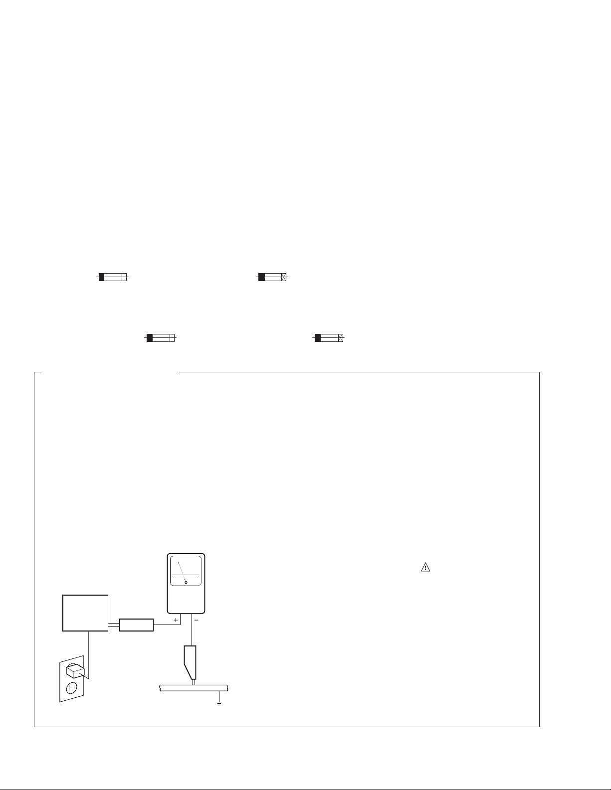
1. SAFETY PRECAUTIONS
The following check should be performed for the
continued protection of the customer and service
technician.
LEAKAGE CURRENT CHECK
Measure leakage current to a known earth ground
(water pipe, conduit, etc.) by connecting a leakage
current tester such as Simpson Model 229-2 or
equivalent between the earth ground and all exposed
metal parts of the appliance (input/output terminals,
screwheads, metal overlays, control shaft, etc.). Plug
the AC line cord of the appliance directly into a 120V
AC 60 Hz outlet and turn the AC power switch on. Any
current measured must not exceed 0.5 mA.
Reading should
not be above
0.5 mA
Earth ground
Device
under
test
Also test with plug
reversed
(Using AC adapter
plug as required)
Leakage
current
tester
Test all exposed
metal surfaces
AC Leakage Test
ANY MEASUREMENTS NOT WITHIN THE LIMITS
OUTLINED ABOVE ARE INDICATIVE OF A POTENTIAL SHOCK HAZARD AND MUST BE CORRECTED BEFORE RETURNING THE APPLIANCE
TO THE CUSTOMER.
2. PRODUCT SAFETY NOTICE
Many electrical and mechanical parts in the appliance have special safety related characteristics. These
are often not evident from visual inspection nor the
protection afforded by them necessarily can be obtained by using replacement components rated for
voltage, wattage , etc. Replacement parts which have
these special safety characteristics are identified in
this Service Manual.
Electrical components having such features are
identified by marking with a
on the parts list in this Service Manual.
The use of a substitute replacement component which
does not have the same safety characteristics as the
PIONEER recommended replacement one, shown in
the parts list in this Service Manual, may create shock,
fire, or other hazards.
Product Safety is continuously under review and
new instructions are issued from time to time. For
the latest information, always consult the current
PIONEER Service Manual. A subscription to, or additional copies of, PIONEER Service Manual may be
obtained at a nominal charge from PIONEER.
on the schematics and
2
Page 3
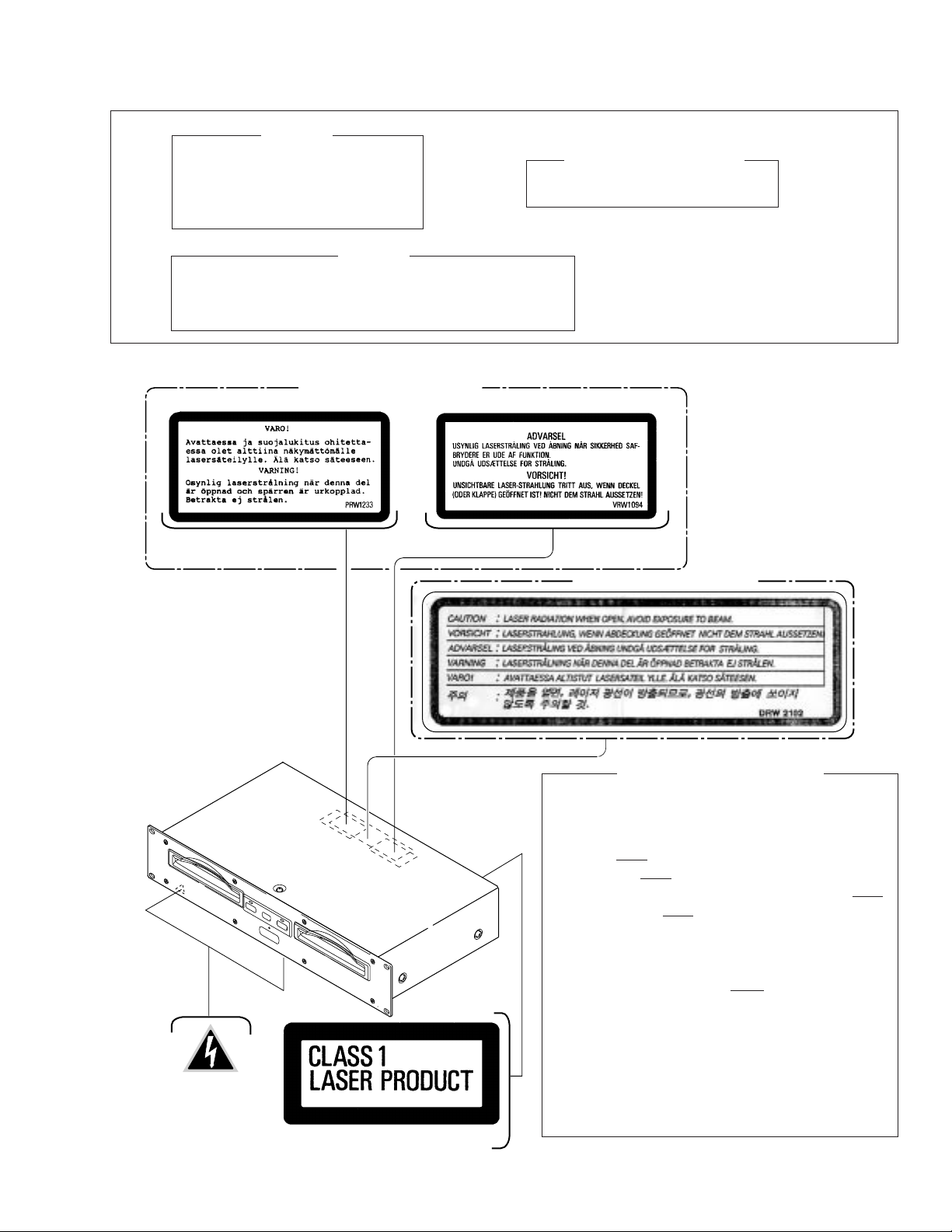
CMX-3000, CU-V163
THIS PIONEER APPARATUS CONTAINS
LASER OF CLASS 1.
SERVICING OPERATION OF THE APPARATUS
SHOULD BE DONE BY A SPECIALLY
INSTRUCTED PERSON.
The AEL(accessible emission level) of the laser power output is less then CLASS 1
but the laser component is capable of emitting radiation exceeding the limit for
CLASS 1.
A specially instructed person should servicing operation of the apparatus.
LABEL CHECK
IMPORTANT
LASER DIODE CHARACTERISTICS
MAXIMUM OUTPUT POWER: 5 mW
WAVELENGTH: 780 – 785 nm
WARNING !
CMX-3000/ WYXJ type Only
CMX-3000/ RLBXJ type Only
CMX-3000/ KUCXJ type Only
Printed on the Rear Panel.
Additional Laser Caution
1. Laser Interlock Mechanism
The position of the switch (S801,S901) for detecting loading
completion is detected by the system microprocessor, and
the design prevents laser diode oscillation when the switch
is not in LPS1 terminal side (when the mechanism is not
clamped and LPS1 signal is high level.) Thus, the interlock
will no longer function if the switch is deliberately set to LPS1
terminal side. ( if LPS1 signal is low level ).
In the test mode∗ the interlock mechanism will not function.
Laser diode oscillation will continue, if pin 9 of TA2153FN
(IC1010, IC1003) on the MAIN ASSY is connected to GND,
or pin 10 of IC1010, IC1003 (LDON) is connected to low
level (ON), or else the terminals of Q1003, Q1229 are
shorted to each other (fault condition).
Note: S801, IC1010 and Q1003 (Player A Side)
S901, IC1003 and Q1229 (Player B side)
2. When the cover is opened, close viewing of the objective
lens with the naked eye will cause exposure to a Class 1
laser beam.
∗ : Refer to page 55.
3
Page 4
CMX-3000, CU-V163
SERVICE INFORMATION
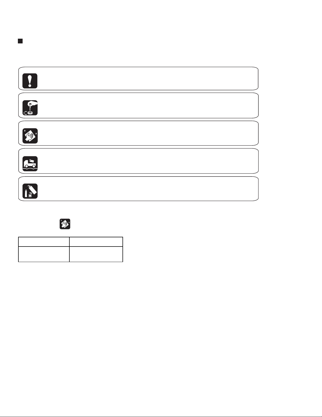
[ Important symbols for good services ]
In this manual, the symbols shown-below indicate that adjustments, settings or cleaning should be made securely.
When you find the procedures bearing any of the symbols, be sure to fulfill them:
1. Product safety
You should conform to the regulations governing the product (safety, radio and noise, and other regulations), and
should keep the safety during servicing by following the safety instructions described in this manual.
2. Adjustments
To keep the original performances of the product, optimum adjustments or specification confirmation is indispensable.
In accordance with the procedures or instructions described in this manual, adjustments should be performed.
3. Cleaning
For optical pickups, tape-deck heads, lenses and mirrors used in projection monitors, and other parts requiring cleaning,
proper cleaning should be performed to restore their performances.
4. Shipping mode and shipping screws
To protect the product from damages or failures that may be caused during transit, the shipping mode should be set or
the shipping screws should be installed before shipping out in accordance with this manual, if necessary.
5. Lubricants, glues, and replacement parts
Appropriately applying grease or glue can maintain the product performances. But improper lubrication or applying
glue may lead to failures or troubles in the product. By following the instructions in this manual, be sure to apply the
prescribed grease or glue to proper portions by the appropriate amount.For replacement parts or tools, the prescribed
ones should be used.
[ NOTES ON SERVICING ]
7 CLEARNING
Before shipping out the product, be sure to clean the following positions by using the prescribed cleaning tools:
Position to be cleaned Cleaning tools
Pickup leneses Cleaning liquid : GEM1004
Cleaning paper : GED-008
4
Page 5
CMX-3000, CU-V163
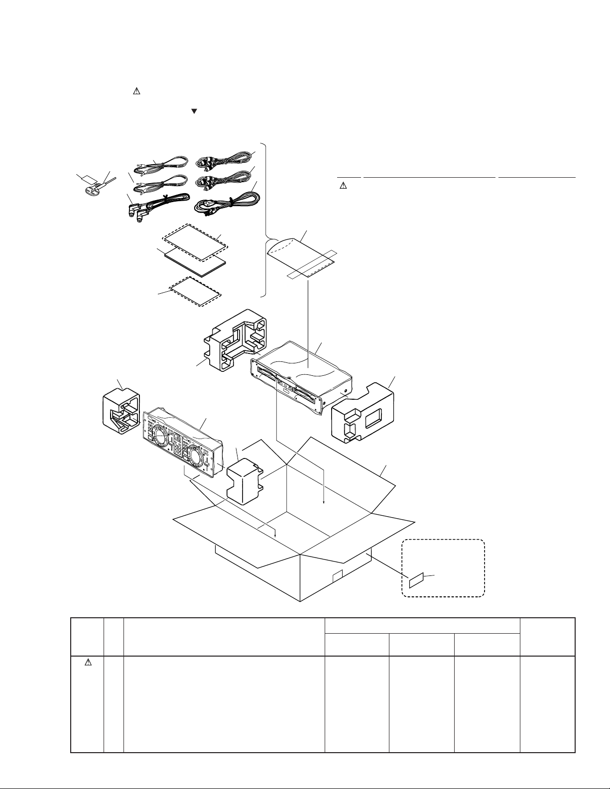
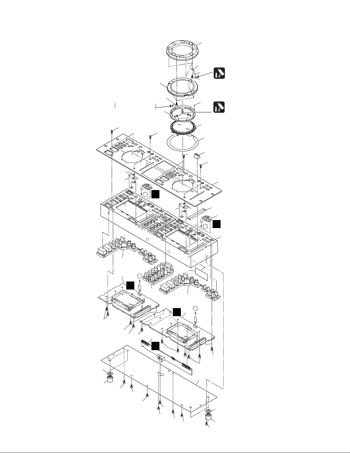
2. EXPLODED VIEWS AND PARTS LIST
NOTES:• Parts marked by "NSP" are generally unavailable because they are not in our Master Spare Parts List.
The mark found on some component parts indicates the importance of the safety factor of the part.
•
Therefore, when replacing, be sure to use parts of identical designation.
Screws adjacent to mark on the product are used for disassembly.
•
For the applying amount of lubricants or glue, follow the instructions in this manual.
•
(In the case of no amount instructions, apply as you think it appropriate.)
2.1 PACKING
4
6
7
3
5
14
RLBXJ type Only
7
KUXJ type Only
2
8
8
1
9
(1) PACKING PARTS LIST
Mark No. Description Part No.
1 AC Power Cord
NSP 2 Limited warranty
NSP 9 Polyethylene Bag Z21-038
13
NSP 15 Label
3 Specialized connection cable for
the remote controller (L=3 m) DDE1122
4 Forced ejection pin DEX1013
5 Operating Instructions
6 Caution Tag DRW1897
7 Control cord (L=1 m) PDE1267
8 Audio cable (L=1.5 m) VDE1064
10 Pad A DHA1529
11 Pad B DHA1530
12 Packing Case
13 Sheet RHX1006
14 Caution 220V Label
See Contrast table (2)
See Contrast table (2)
See Contrast table (2)
See Contrast table (2)
See Contrast table (2)
See Contrast table (2)
11
10
13
11
10
12
KUCXJ and WYXJ
type Only
15
(2) CONTRAST TABLE
CMX-3000/KUXJ, WYXJ and RLBXJ are constructed the same except for the following:
No.
Symbol and DescriptionMark
KUCXJ Type WYXJ Type RLBXJ Type
Part No.
Remarks
1 AC Power Cord ADG7022 ADG1154 ADG1154
NSP 2 Limited warranty ARY7043 Not used Not used
5 Operating Instructions (English) DRB1307 Not used Not used
5 Operating Instructions Not used DRB1306 Not used
(English/ French/ German/ Italian/ Dutch/ Spanish)
5 Operating Instructions (English/ Spanish/ Chinese) Not used Not used DRB1308
12 Packing Case DHG2160 DHG2158 DHG2161
14 Caution 220V Label Not used Not used ARR1003
NSP 15 Label VRW1629 VRW1629 Not used
5
Page 6
CMX-3000, CU-V163
2.2 EXTERIOR SECTION
6
C
41
41
5555
39
Refer to
"2.3 SLOT-IN MECHANISM
ASSY"
20
20
B
B
5
30
36
34
A
J
24
G
21
H
45
45
47
4
J
41
I
29
41
H
40
48
12
45
C
B
41
26
28
G
B
53
20
H
41
32
49
44
50
42
42
41
17
8
17
41
18
14
I
E
9
41
13
52
26
57
47
L
M
14
9
N
22
1
37
44
41
45
41
45
41
48
28
48
41
E
11
18
12
F
A
41
K
40
45
23
F
E
54
28
41
41
47
D
41
51
2
43
F
F
E
D
C
35
10
15
3
41
G
38
D
27
55
41
K
L
41
41
7
M
N
46
56
33
58
19
A
56
31
46
25
41
39
19
Refer to
"2.3 SLOT-IN MECHANISM ASSY"
5541
29
6
Page 7
(1) EXTERIOR SECTION PARTS LIST
Mark No. Description Part No.
1 MAIN ASSY DWG1556
2 PWRB ASSY
3 ACIN ASSY
4 REGB ASSY
5 FRSW ASSY DWS1314
See Contrast table (2)
See Contrast table (2)
See Contrast table (2)
CMX-3000, CU-V163
Mark No. Description Part No.
31 Front Panel DNB1098
32 Bonnet Case DNE1409
33 Function Panel DNK3944
34 Power Knob Caver DNK3945
35 Power Knob DNK3946
6 SLM1 ASSY DWS1315
7 SLM2 ASSY DWS1316
8 JACB ASSY
9 Leadcard 16p DDD1194
10 Power Transfomer
11 Connector Ass’y PF05FE-D17
12 Connect0r Ass’y (6p) PF06PP-B47
13 Connector Assy PF09EE-D25
14 Connector Ass’y PG03KK-E15
15 Fuse (FU101)
16 • • • • •
17 Rubber Spacer DEB1455
NSP 18 Silicon Rubber D5 L DEB1456
19 Insulator DEC2348
20 Front Sheet B DEC2467
NSP 21 Chassis DNA1277
22 Rear Panel
23 PCB Frame DNH2502
24 Panel Stay DNH2503
25 Bottom Plate DNH2505
26 Heat Sink DNH2508
27 Locking Card Spacer VEC1596
28 Sheet DED1159
29 Earth Spring DBH1398
30 Eject Knob DEB1503
See Contrast table (2)
See Contrast table (2)
See Contrast table (2)
See Contrast table (2)
36 Slide SW Knob DNK3947
NSP 38 Label VRW-548
37 65 Label
39 POM Bush (M3) DEC2397
40 Screw BBZ26P060FMC
41 Screw BBZ30P060FMC
42 Screw BBZ30P060FZK
43 Screw BBZ40P060FMC
44 Screw BBZ40P060FZK
45 Screw BPZ30P080FZK
46 Screw CBZ30P080FZK
47 Rivet (Plastic) RBM-003
48 Cord Clamper (Steel) RNH-184
49 Caution Label HE
50 Caution Label
51 Trans Sheet DEC2280
52 Caution Label
53 Screw Guard DEB1447
54 Binder ZCA-SKB90BK
55 Screw BBZ30P080FMC
NSP 56 Caution Label
57 Protect Sheet
58 Spacer (PEE) DEC2470
See Contrast table (2)
See Contrast table (2)
See Contrast table (2)
See Contrast table (2)
See Contrast table (2)
See Contrast table (2)
(2) CONTRAST TABLE
CMX-3000/KUXJ, WYXJ and RLBXJ are constructed the same except for the following:
No.
Symbol and DescriptionMark
KUCXJ Type WYXJ Type RLBXJ Type
2 PWRB ASSY DWR1345 DWR1345 DWR1348
3 ACIN ASSY DWR1349 DWR1346 DWR1346
4 REGB ASSY DWR1357 DWR1347 DWR1347
8 JACB ASSY DWX2214 DWX2200 DWX2200
10 Power Transfomer (AC120V) DTT1161 Not used Not used
10 Power Transfomer (AC220-240V) Not used DTT1160 Not used
10 Power Transfomer (AC110-120V/220-240V) Not used Not used DTT1162
15 Fuse (FU101: 1.6A) REK1077 Not used Not used
15 Fuse (FU101: 1.0A) Not used REK1022 REK1022
22 Rear Panel DNC1586 DNC1585 DNC1587
37 65 Label ARW7050 Not used Not used
49 Caution Label HE Not used PRW1233 Not used
50 Caution Label Not used VRW1094 Not used
NSP 56 Caution Label DRW1975 Not used Not used
52 Caution Label Not used Not used DRW2102
57 Protect Sheet Not used DEC2466 DEC2466
Part No.
Remarks
7
Page 8
CMX-3000, CU-V163
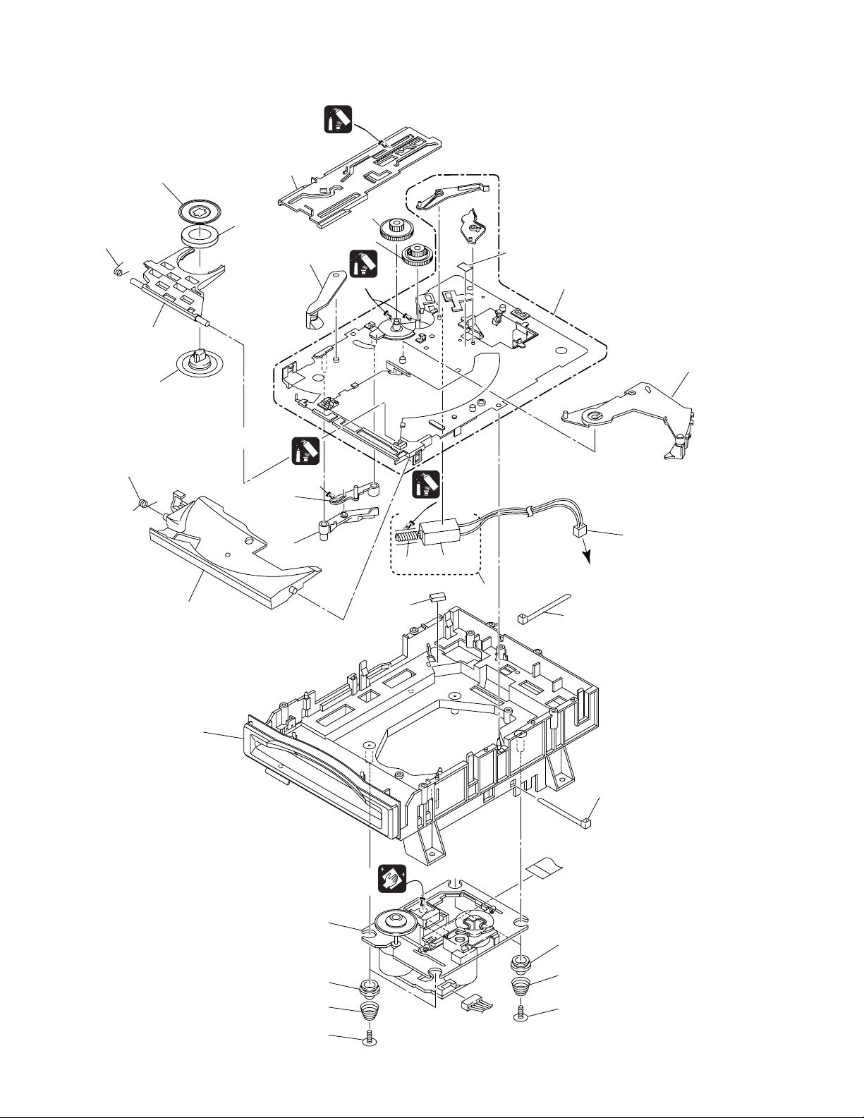
2.3 SLOT-IN MECHANISM SECTION
Paint grease the inner
surface of the wall.
11
13
Grease
Grease
(ZLB-PN397B)
(GYA1001)
10
7
Paint on side of axle.
12
22
21
Grease
Grease
(ZLB-PN397B)
(GYA1001)
9
16
15
17
23
Paint grease the inner
Paint grease the inner
surface of the wall.
surface of the wall.
Dyefree
8
Dyefree
(ZLX-ME413A)
(GEM1023)
18
19
Grease
Grease
(ZLB-PN397B)
(GYA1001)
20
1
24
To MAIN Assy
28
14
5
26
25
26
Cleaning liquid (GEM1004)
Cleaning paper (GED-008)
27
6
6
3
4
2
2
8
Page 9

SLOT-IN MECHANISM SECTION PARTS LIST
•
Mark No. Description Part No.
1 Connector Ass’y DKP3565
2 Float Fastener DBA1139
3 Float Spring F DBH1491
4 Float Spring R DBH1492
5 Spacer Por (T3) DEB1467
6 Float Rubber DEB1506
7 Clamp Spring DBH1374
8 Guide Spring DBH1375
9 Sw.Lever Spacer (Pet) DEC2420
10 Clamp Magnet DMG1008
11 Yoke DNH2504
12 Loading Lever DNK3406
13 Main Cam DNK3407
14 Disc Guide DNK3478
15 Clamp Arm DNK3576
16 Loading Base Assy-S DEA1022
17 Eject Lever DNK3684
18 Lever AP DNK3835
NSP 20 Worm Gear DNK3410
19 Lever BP DNK3836
CMX-3000, CU-V163
21 Loading Gear DNK3409
22 Drive Gear DNK3565
NSP 24 Loading Motor DXM1173
23 Clamper DNK3949
25 Mecha Base DNK3948
26 Binder ZCA-SKB90BK
27 CD Mechanism DA11T3CNPIO
28 Loading Motor Assy-S DXX2510
9
Page 10
CMX-3000, CU-V163
2.4 REMOTE CONTROLLER (CU-V163)
16
12
10
6
23
Super X
(GYL1004)
A hand driver fastens a screw.
The screw tightening torque
0.098 ± 0.01% [N • m]
29
30
13
A
20
1
A
6
14
29
4
29
19
24
8
25
29
Grease is applied to three
places every two pieces.
Grease
(GYA1014)
22
J
13
30
26
9
5
L
B
15
10
7
18
28
28
27
28
I
27
28
28
21
3
M
27
28
17
K
28
27
27
20
2
B
28
28
11
7
18
28
Page 11

REMOTE CONTROLLER (CU-V163) PARTS LIST
•
Mark No. Description Part No.
1 CNTA ASSY DWG1551
2 CNTB ASSY DWG1552
3 CNNB ASSY DWG1553
4 PHTA ASSY DWG1554
5 PHTB ASSY DWG1555
6 Screw ABA7022
7 CR Spacer DEB1524
8 Jog Sheet A DEC2468
9 Slide VR Packing DED1157
10 J Magnet DMG1006
11 Rear Panel DNC1590
12 Magnet Stay DNF1668
13 Earth Plate DNH2506
14 Retainer DNK3952
15 Panel Base DNK3953
16 Jog Ring DNK3954
17 Screw (Steel) PBA1096
18 Foot (Rubber) REC1263
19 Steel Ball VNX1006
20 Select Knob 1 DEB1504
CMX-3000, CU-V163
21 Select Knob 2 DEB1505
22 Control Panel DNB1099
23 Jog Dial DNK3950
24 Display Plate DNK3951
25 Slide Knob DNK3955
26 65 Label ARW7050
27 Screw BBZ30P060FMC
28 Screw BPZ30P080FZK
29 Screw CBZ30P080FZK
30 Washer WH30FUC
11
Page 12
1
23
CMX-3000, CU-V163
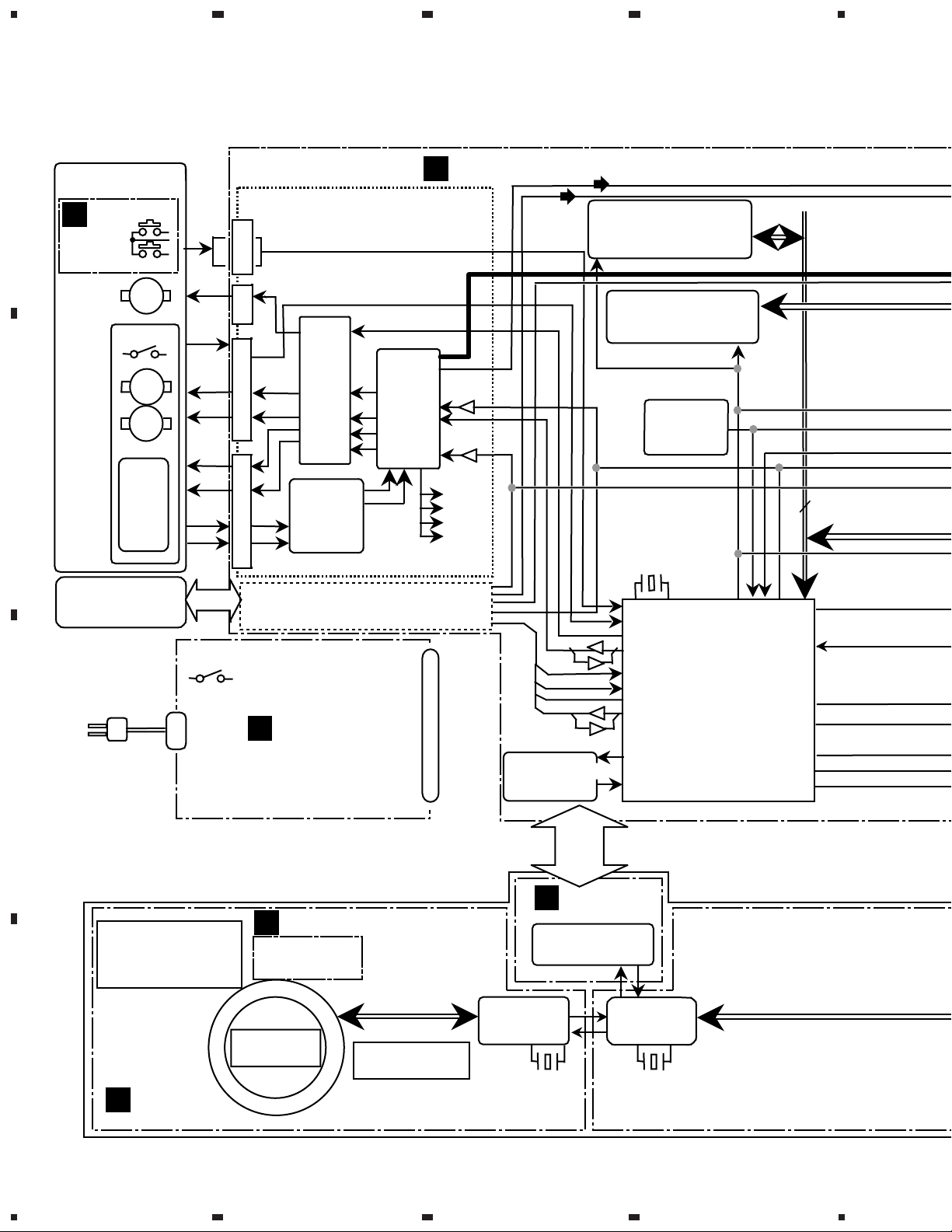
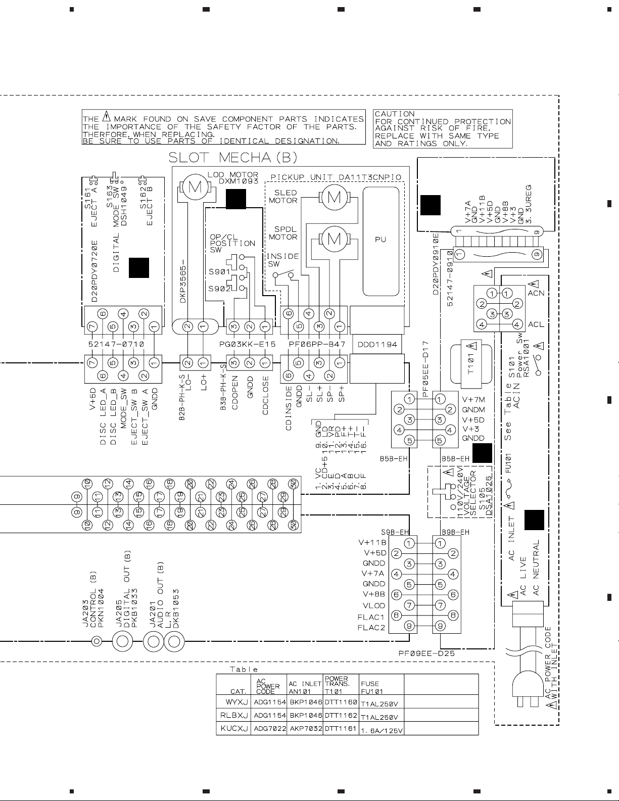
3. BLOCK DIAGRAM AND SCHEMATIC DIAGRAM
3.1 BLOCK DIAGRAM
A
B
C
Slot Mecha (A)
Slot mecha
A
SLM1 ASSY
C
OP/CL
POSITION SW
Lod
M
INSIDE SW
sled
M
Spdl
M
PU
Slot mecha
B
RSA1001
Sw:
1
2
AC Power Cord
1
2
Remoto Controller Section
Function Key : A
CN801
3
2
1
J4
2
1
CN2
6
INSIDE
5
4
3
2
1
CN1
#
@
!
~
|
1
PL(A) Servo Circuit
LOAD SW
B T L
driver
IC1011
LA6562
Head AMP
IC1010
TA2153FN
PL(B) Servo Circuit
PWRB ASSY
F
Connector pin name
GNDD
GNDD
J
JOG/ENCODER
GP1S94 x2
RXD
3
V+8B
4
PHTA ASSY
Servo
processor
IC1005
TC9495F
CN105
FLAC1
5
TXD
6
A
MAIN ASSY
MCK
SBOK
SUBQ
SBSY
SFSY
toFPGA
1
V+11B
2
V+5D
3
GNDD
4
V+7A
5
GNDD
6
V+8B
7
VLOD
8
FLAC1
9
FLAC2
VLOD
7
FLAC2
8
(DOA)
(DOB)
/
4
/
4
Communication
I/F
JA701
JA207
M
CNNB ASSY
Communication
I/F
FLASH ROM(8M)
DSS1132 12.0MHz
IC1200
DYW1701
SDRAM(128M)
IC1408
K4S281632C
RESET
IC1022
M51957
48.0MHz =
Lod_Sw
INSD
LOD(A)
COM(A)
Lod_Sw
INSD
LOD(B)
COM(B)
IC1204
Micro Computer
(MINIDIN8P)
4
CLK
16
DONE
PRGM
RESET
SET
MUTE
COM
IC301 IC501
FL
D
I
CNTA ASSY
12
1234
DEL1047
Slider-
60mm
DCV1011
DSS1131
4MHz
PD5764A
DSS1131
4MHz
Control ICControl IC
Page 13
5
678
CMX-3000, CU-V163
(DOA)
(DOB)
Spartan
CLK
PRGM
DONE
RESET
MM1561
IC1208
IC1406
L
JOG/ENCODER
Reg1.8v
NJM2870F18
Reg1.8v
PHTB ASSY
GP1S94 x2
S/P I/O
S/P I/O
P/S I/O
P/S I/O
P/S
BCK/ LRC
IC1409
Gerenation
XC2S30-5TQ144C
AUDIO (A)
AUDIO (B)
CLK
RESET
Req
Valid
COM
AUDIO(A)
DSP
XCA56367
IC1402
AUDIO(B)
Function Key : B
LRCK IN
Divider
Comparator
Divider
Comparator
4
/
CN1011
AUDIO(B)
AUDIO(A)
(DA)
(DB)
MCK(A)
*
(DA)
I
_
(DB)
MCK(B)
+
I
£
909
4
3
2
(DOA)
(DOB)
P L L (A)
VCO
3 Signals
Conversion
LPF
P L L (B)
VCO
3 Signals
Conversion
LPF
IC1009
NJM2870F25
Reg2.5v
CN201
*
I
_
+
I
£
0
(DA)
(DB)
(DOA)
(DOB)
DAC
PE8001
IC201
DAC
(B)
PE8001
IC202
SIGNAL ROUTE
(A)
: PB A AUDIO SIGNAL
(B)
: PB B AUDIO SIGNAL
: DIGITAL DATA A SIGNAL
: DIGITAL DATA B SIGNAL
: DIGITAL AUDIO A SIGNAL
: DIGITAL AUDIO B SIGNAL
-
=
CN201
-
=
CN1011
JACB ASSY
Master Clock
VSS1084
16.9344MHz
CN201CN1011
^
^
&
&
¢
¢
∞
∞
IC204
NJM4558
4
3
2
EJECT sw A/B
J161CN1012
(DOA)
(DOB)
E
(A)(A)
(B)
DIGITAL OUT
On/off SW
FRSW ASSY
DIGITAL
OUT A
DIGITAL
OUT B
CONTROL A
CONTROL B
AUDIO
OUT A
AUDIO
OUT B
B
A
B
C
FL
DEL1047
5
Slider-
DCV1011
K
CNTB ASSY
60mm
D
13
6
7
8
Page 14
1
CMX-3000, CU-V163
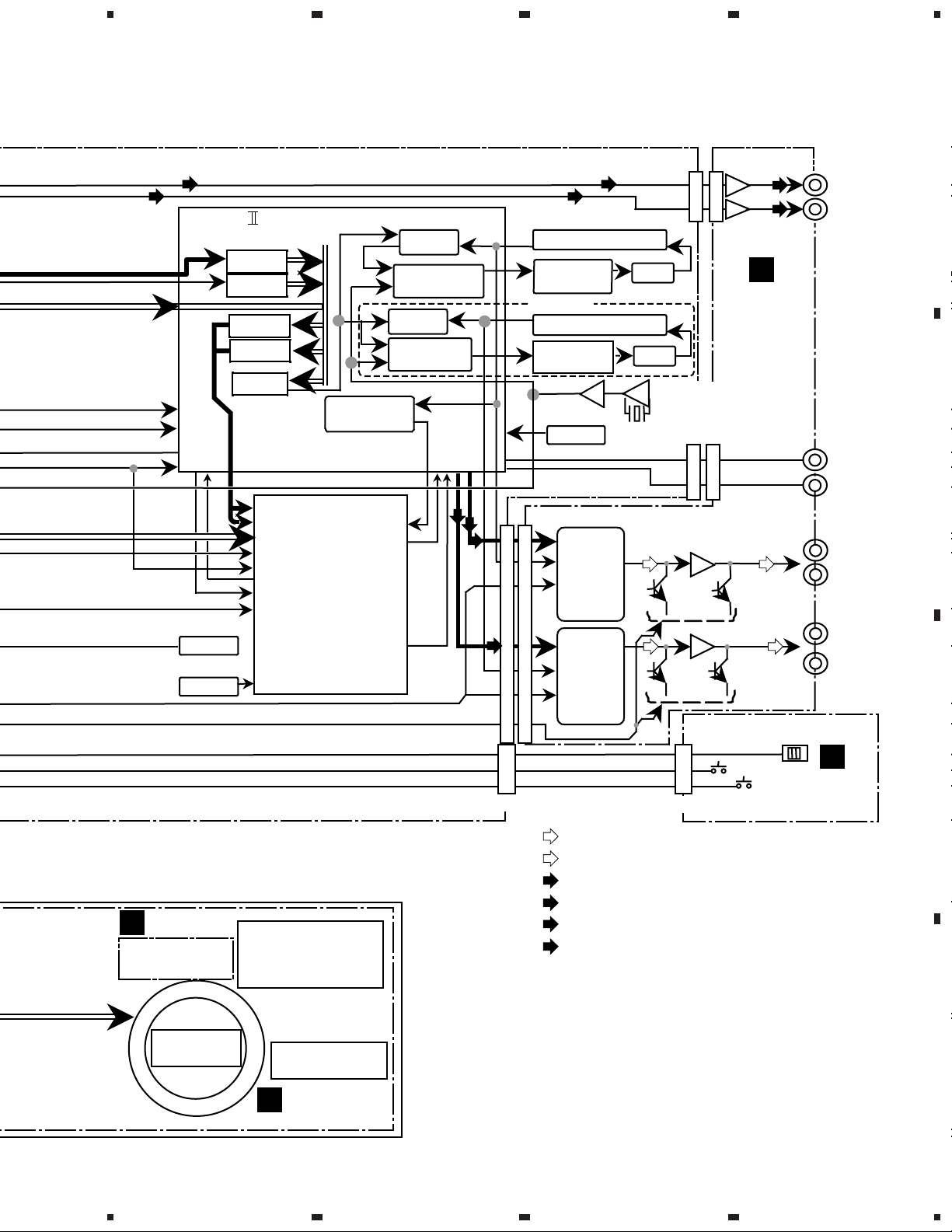
3.2 OVERALL WIRING DIAGRAM
A
L
PHTB ASSY
(DWG1555)
J502
CN501
CN503
23
CN703
C
SLM1 ASSY
(DWS1315)
4
B
CN504
CN704
J4
CN801
CN2
CN1
K
CNTB ASSY
(DWG1552)
CN1008
CN303
C
CN702
CNNB ASSY (DWG1553)
M
E
CN1006
CN1007
MAIN ASSY
A
(DWG1556)
JACB ASSY
(KUCXJ: DWX2214)
(WYXJ: RLBXJ: DWX2200)
CN1010
CN201
CN1009
I
CNTA ASSY
(DWG1551)
CN301
J302
PHTA ASSY
J
D
14
(DWG1554)
1234
JA701
JA207
Page 15
5
678
CMX-3000, CU-V163
Note : When ordering service parts, be sure to refer to "EXPLODED VIEWS and P AR TS LIST" or "PCB PARTS LIST".
REGB ASSY
(WYXJ, RLBXJ: DWR1347)
(KUCXJ:DWR1357)
D
SLM2 ASSY
(DWS1316)
H
J151
A
FRSW ASSY
(DWS1314)
J161
CN1012
B
J4
CN1004
CN901
CN1002
CN2
CN1003
CN1
CN1005
CN1218 CN104
CN202
CN106
CN105
F
CN102CN103
ACIN ASSY
G
B
(KUCXJ: DWR1349)
(WYXJ: RLBXJ: DWR1346)
C
AN101
PWRB ASSY
(KUCXJ, WYXJ: DWR1345)
(RLBXJ: DWR1348)
POWER
REQUIREMENT
REK1022
REK1022
REK1077
5
6
AC220- 240V
60Hz
AC110- 120V/ 220-240V
50/ 60Hz
AC120V
50/ 60Hz
7
15
8
D
Page 16
1
CMX-3000, CU-V163
3.3 MAIN (1/3) ASSY
A
CN1010
(DOB)
CN201
E
(DB)
(DA)
B
(IC1204: 118pin)
(IC1204: 119pin)
(DOA)
(IC1204: 158pin)
(IC1204: 157pin)
(IC1204: 165pin)
(IC1204: 164pin)
(IC1204: 11pin)
(IC1204: 10pin)
A 2/3
A 1/3
A 3/3
A 1/3
A 1/3,2/3
A 1/3
A 2/3
A 2/3
23
A 1/3
A 3/3
A 2/4
A 1/3
(L)
(L)
A 3/3
A 2/3
A 3/3
A 2/3
4
MAIN ASSY
(DWG1556)
A 1/3
A 2/3
(L)
(L)
A 2/3
A 1/3
(L)
(L)
A 1/3,2/3
A 1/3
A 3/3
C
A 3/3
A 1/3
A 1/3
A 2/3,3/3
A 2/3
D
A 3/3
16
A 2/3
A 3/3
1/3
A
1234
A 1/3
Page 17
5
678
CMX-3000, CU-V163
A 3/3
CN1218
CN104
F
A 1/3
: The power supply is shown with the marked box.
(L)
(L)
A 3/3
A
B
SIGNAL ROUTE
(DA)
: DIGITAL DATA A SIGNAL
(DB)
: DIGITAL DATA B SIGNAL
(DOA)
: DIGITAL OUT A SIGNAL
(DOB)
: DIGITAL OUT B SIGNAL
(L)
: LOADING MOTOR SIGNAL
A 1/3
C
DYW1701
A 1/3
D
A 2/3
A 2/3
A 2/3
1/3
A
5
6
7
8
17
Page 18
1
23
CMX-3000, CU-V163
3.4 MAIN (2/3) and FRSW ASSYS
4
A
VCO Adjust -b
VCO Adjust -a
I
A 1/3
A 1/3
CN1012
B
A 1/3
A 1/3
A 1/3
A 1/3
A 1/3
A 1/3
C
A 1/3
A 1/3
A 1/3
A 1/3
(DA)
A 3/3
FRSW ASSY
B
(DWS1314)
(DB)
A 1/3, 2/3
A 1/3, 3/3
J161
D
A 1/3
A 3/3
18
A 1/3
A 1/3
2/3
A
1234
B
Page 19
5
678
CMX-3000, CU-V163
A 2/3
MAIN ASSY
(DWG1556)
A
B
A 1/3
SIGNAL ROUTE
(DA)
: DIGITAL DATA A SIGNAL
: DIGITAL DATA B SIGNAL
(DB)
A 1/3
C
A 2/3
A 1/3
A 1/3
A 1/3
D
2/3
A
5
6
7
8
19
Page 20
1
23
CMX-3000, CU-V163
3.5 MAIN (3/3), SLM1 and SLM2 ASSYS
4
A 2/3
A
A 1/3
A 3/3
MAIN ASSY
(DWG1556)
C
SLM1 ASSY
(DWS1315)
A 1/3
CN801
(DOA)
A 1/3
A 1/3
(DA)
B
A 2/3
(DOA)
CN1006
A 1/3
A 1/3
(TS)
(RF)
(FS)
(TS)
B
E
C
Q1002
C
(TS) (TS)
DTC114TK
(TS)
(RF)
(FS)
(RF)
3
4
1
2
(TS)
(FS)
(FS)
(TS)
(FS)
RF
FE
(TS)
(FS)
(FS)
(FS)
(TS)
(TS)
6
(L)
(L)
(L)
5
CN1007
CN1008
(L)
(L)
Searvo Mecha
To Slot Mecha (A)
Loading Motor
To Slot Mecha (A)
D
E
B
C
Q1003
2SA1036 (QR)
(FS)
(TS)
(TS)
(FS)
(L)
(L)
A 3/3
A 1/3
A 1/3
: The power supply is shown with the marked box.
To Slot Mecha (A)
Pickup Assy
20
3/3
A
1234
C
Page 21
A 2/3
5
678
CMX-3000, CU-V163
A 1/3
A 1/3
A 2/3
A 1/3
(DOB)
(DB)
(DOB)
(TS)
(RF)
(FS)
(TS)
(FS)
(TS)
CN901
(RF)
: RF SIGNAL ROUTE
(L)
: LOADING MOTOR SIGNAL
(FS)
: FOCUS SERVO SIGNAL
(TS)
: TRACKING SERVO SIGNAL
(DA)
: DIGITAL DATA A SIGNAL
(DB)
: DIGITAL DATA B SIGNAL
: DIGITAL OUT A SIGNAL
(DOA)
: DIGITAL OUT B SIGNAL
(DOB)
D
SLM2 ASSY
(DWS1316)
A 1/3
CN1002
A 1/3
A 1/3
A
B
(FS)
(TS)
(TS)
B
E
C
Q1228
DTC114TK
E
C
2SA1036 (QR)
B
Q1229
(FS)
(RF)
RF
(FS)
(RF)
3
4
1
2
(TS)
FE
(TS)
(FS)
(FS)
(FS)
(TS)
(TS)
6
(L)
(L)
(L)
5
CN1003
C
Searvo Mecha
To Slot Mecha (B)
CN1004
(L)
(L)
Loading Motor
To Slot Mecha (B)
(FS)
(TS)
(TS)
(FS)
A 3/3
(L)
(L)
A 1/3
A 1/3
D
To Slot Mecha (B)
Pickup Assy
3/3
A
5
6
7
D
8
21
Page 22
1
CMX-3000, CU-V163
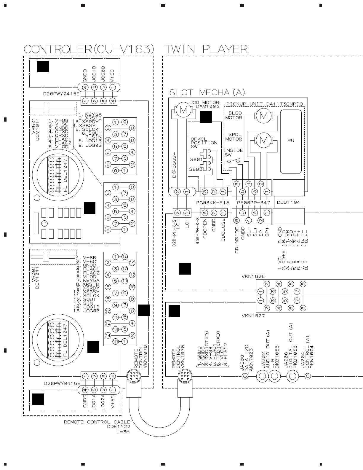
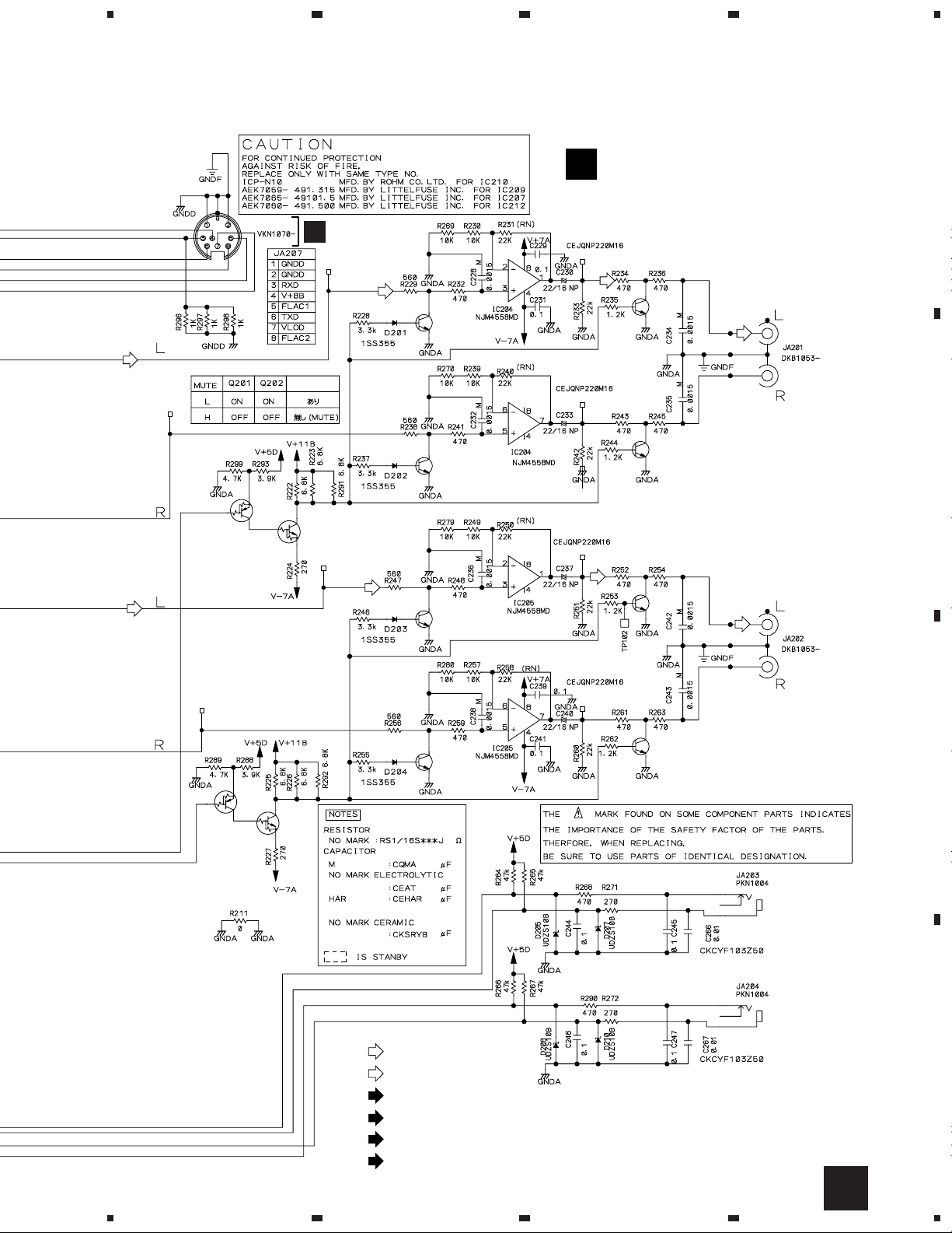
3.6 JACB ASSY
23
4
: The power supply is shown with the marked box.
(1.5A)
A
(0.4A)
CN202
Q171
2SB1237
CN105
F
(500mA)
(315mA)
Q215
2SB1375
B
(DB)
(A)
(B)
(DB)(DB)
JA208
C
AKN7003-
DATA I/O
Q182
DTA143EUA
(DA)
CN201
(DOA)
(DOB)
(DA)
(DOB)
Q213
2SD2412K (RS)
DIGITAL OUT (B)
(DOB)
CN1010
Q214
A
D
(DB)
(DB)
(DOA)
2SD2412K (RS)
DIGITAL OUT (A)
(DOA)
22
(DA) (DA)
E
1234
Page 23
5
678
CMX-3000, CU-V163
JACB ASSY
E
(KUCXJ: DWX2214)
A
(WYXJ: RLBXJ: DWX2200)
JA207
(A)
TP3
Q201
DTA124EUA
(B)
M
AUDIO OUT
Q202
DTC124EUA
JA701
TP1
TP5
(B)
TP2
(A)
Q205
2SD2114 K (VW)
Q207
2SD2114 K (VW)
Q209
2SD2114 K (VW)
(A)
TP4
TP6
TP6
(B)
2SD2114 K (VW)
Q206
Q208
2SD2114 K (VW)
2SD2114 K (VW)
Q210
(A)
AUDIO OUT (B)
B
(B)
AUDIO OUT (A)
TP7
Q203
DTA124EUA
Q204
DTC124EUA
Q211
2SD2114 K (VW)
SIGNAL ROUTE
(A)
: PB A AUDIO SIGNAL
(B)
: PB B AUDIO SIGNAL
(DA)
: DIGITAL DATA A SIGNAL
: DIGITAL DATA B SIGNAL
(DB)
(DOA)
: DIGITAL OUT A SIGNAL
(DOB)
: DIGITAL OUT B SIGNAL
TP8
Q212
2SD2114 K (VW)
C
CONTROL (B)
CONTROL (A)
D
E
5
6
7
8
23
Page 24
1
CMX-3000, CU-V163
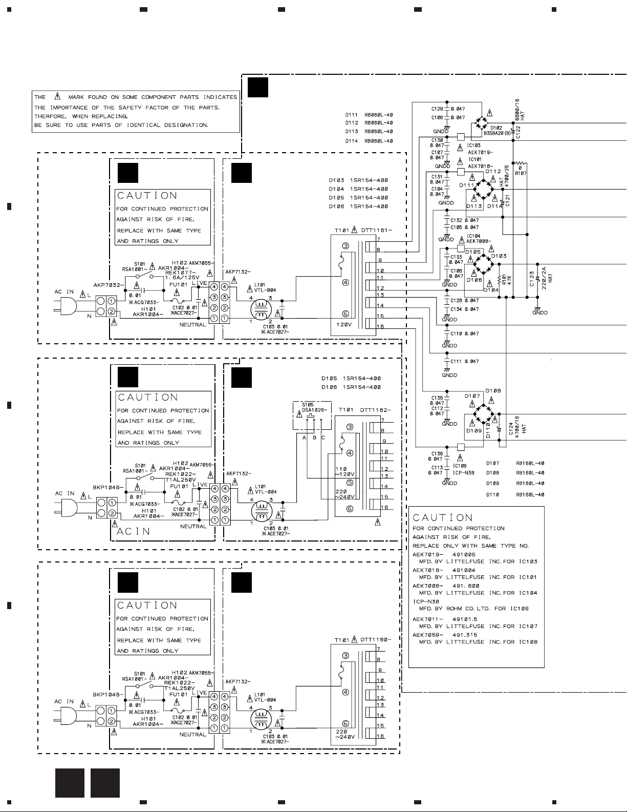
3.7 PWRB, REGB and ACIN ASSYS
A
KUCXJ type
AN101
B
AC CORD: ADG7022AC120V 60Hz
G
ACIN ASSY
(DWR1349)
CN102
23
F
PWRB ASSY
(KUCXJ: DWR1345)
(WYXJ: DWR1345)
(RLBXJ: DWR1348)
PWRB ASSY
F
(DWR1345)
CN103
4
(5A)
(4A)
(800mA)
RLBXJ type
AN101
C
AC CORD: ADG1154AC110-120V/ 220-240V
50/ 60Hz
WYXJ type
G
G
ACIN ASSY
(DWR1346)
CN102
ACIN ASSY
(DWR1346)
F
CN103
F
PWRB ASSY
(DWR1348)
PWRB ASSY
(DWR1345)
(800mA)
(1.5A)
CN102
D
AC CORD: ADG1154AC220-240V 50/ 60Hz
24
F
AN101
G
1234
CN103
Page 25
5
678
CMX-3000, CU-V163
A
CN106 J151
B
(315mA)
(1.5A)
CN104
CN105
CN1218
A
CN202
E
REGB ASSY
(KUCXJ: DWR1357)
H
(WYXJ, RLBXJ: DWR1347)
C
D
H
5
6
7
8
25
Page 26
1
23
CMX-3000, CU-V163
3.8 CNTA and PHTA ASSYS
M
4
CN702
A
CN303
Q369 2SC4081 (R/S)
Q361 2SC4081 (R/S)
Q372 2SC4081 (R/S)
Q373 2SC4081 (R/S)
Q368 2SC4081 (R/S)
B
Q370 2SC4081 (R/S)
Q371 2SC4081 (R/S)
Q362 2SC4081 (R/S)
Q363 2SC4081 (R/S)
Q364 2SC4081 (R/S)
Q365 2SC4081 (R/S)
Q366 2SC4081 (R/S)
Q367 2SC4081 (R/S)
C
SWITCHES
S301 : 1
S302 : ¡
S303 : 4
S304 : ¢
S305 : TIME MODE/ AUTO CUE
S306 : CD TEXT/ WAVE
S307 : PITCH BEND [ + ]
S308 : PITCH BEND [ - ]
S311 : MASTER TEMPO
S312 : TEMPO RANGE
S313 : 0 (EJECT)
S341 : 6
S342 : CUE
S343 : IN/REALTIME CUE
D
S344 : OUT/ OUT ADJ
S345 : JOG MODE
S346 : EXIT/RELOOP
S347 : EMERGENCY LOOP
26
I
1234
Page 27

5
678
CMX-3000, CU-V163
: The power supply is shown with the marked box.
CNTA ASSY
I
(DWG1551)
CN301
J302
PHTA ASSY
J
(DWG1554)
A
B
C
Q410
2SC4081 (R/S)
2SC4081 (R/S)
D
7
I
J
8
27
Q409
Q408
Q406
Q404
2SC4081 (R/S)
2SC4081 (R/S)
Q403
5
2SC4081 (R/S)
2SC4081 (R/S)
6
Page 28

1
23
CMX-3000, CU-V163
3.9 CNTB and PHTB ASSYS
4
M
CN704
M
CN703
A
CN504 CN503
Q569 2SC4081 (R/S)
Q561 2SC4081 (R/S)
Q572 2SC4081 (R/S)
Q573 2SC4081 (R/S)
Q568 2SC4081 (R/S)
B
Q570 2SC4081 (R/S)
Q571 2SC4081 (R/S)
Q562 2SC4081 (R/S)
Q563 2SC4081 (R/S)
Q564 2SC4081 (R/S)
Q565 2SC4081 (R/S)
Q566 2SC4081 (R/S)
Q567 2SC4081 (R/S)
C
SWITCHES
S501 : 1
S502 : ¡
S503 : 4
S504 : ¢
TIME MODE/ AUTO CUE
S505 :
S506 : CD TEXT/ WAVE
S507 : PITCH BEND [ + ]
S508 : PITCH BEND [ - ]
S511 : MASTER TEMPO
S512 : TEMPO RANGE
S513 : 0 (EJECT)
S514 : BPM S SYNC
S515 : RELAY PLAY
S521 : HOT CUE 1 - B
S522 : HOT CUE 2 - B
S523 : HOT CUE 3 - B
S524 : HOT CUE REC - B
S525 : AUTO - B
S526 : TAB - B
S531 : HOT CUE 1 - A
S532 : HOT CUE 2 - A
S533 : HOT CUE 3 - A
S534 : HOT CUE REC - A
S535 : AUTO - A
D
S536 : TAB S541 : 6
S542 : CUE
S543 : IN/ REALTIME CUE
S544 : OUT/ OUT ADJ
S545 : JOG MODE
S546 : EXIT/ RELOOP
S547 : EMERGENCY LOOP
28
K
1234
Page 29

5
678
CMX-3000, CU-V163
CNTB ASSY
K
(DWG1552)
: The power supply is shown with the marked box.
CN501
J502
PHTB ASSY
L
(DWG1555)
A
B
Q601
2SC4081 (R/S)
Q602
2SC4081 (R/S)
5
Q603
2SC4081 (R/S)
Q604
2SC4081 (R/S)
Q606
2SC4081 (R/S)
Q608
2SC4081 (R/S)
Q609
2SC4081 (R/S)
6
Q610
2SC4081 (R/S)
Q611
2SC4081 (R/S)
Q612
2SC4081 (R/S)
Q613
2SC4081 (R/S)
7
Q614
2SC4081 (R/S)
Q615
2SC4081 (R/S)
Q616
2SC4081 (R/S)
K
Q617
2SC4081 (R/S)
L
8
Q618
2SC4081 (R/S)
29
C
D
Page 30

1
CMX-3000, CU-V163
3.10 CNNB ASSY
A
CN504
K
B
CN704
CN703
23
: The power supply is shown with the marked box.
CNNB ASSY
M
(DWG1553)
4
CN503
K
CN702
CN303
I
C
D
30
M
1234
Page 31

Waveforms
1
2
1
2
IC1010- 16pin (FE)
IC1003- 16pin (FE)
V: 0.5V/div. H: 5mS/div.
IC1010- 14pin (TE)
IC1003- 14pin (TE)
V: 1V/div. H: 5mS/div.
Mode: Focus IN
2
2
IC1010- 14pin (TE)
IC1003- 14pin (TE)
V: 1V/div. H: 2mS/div.
Mode: Tracking Open
2
2
IC1010- 14pin (TE)
IC1003- 14pin (TE)
V: 0.5V/div. H: 2mS/div.
Mode: 1 Track Jump
3
3
IC1010- 28pin (RFO)
IC1003- 28pin (RFO)
V: 500mV/div. H: 500nS/div.
Mode: RF (Play Mode x1)
3
3
IC1010- 28pin (RFO)
IC1003- 28pin (RFO)
V: 500mV/div. H: 200nS/div.
Mode: RF (Play Mode x2)
4
4
IC1010- 25pin (RFGO)
IC1003- 25pin (RFGO)
V: 500mV/div. H: 500nS/div.
Mode: AGC RF (Play Mode x1)
4
4
IC1010- 25pin (RFGO)
IC1003- 25pin (RFGO
V: 500mV/div. H: 200nS/div.
Mode: AGC RF (PLAY MODE x2)
2
5
2
5
6
IC1010- 14pin (TE)
IC1003- 14pin (TE)
V: 1V/div. H: 0.2S/div.
IC1011- 6pin (SL+)
IC1004- 6pin (SL+)
V: 2V/div. H: 0.2S/div.
6
IC1011- 7pin (SL-)
IC1004- 7pin (SL-)
V: 2V/div. H: 0.2S/div.
Mode: 1 Track = 16 Track Serch
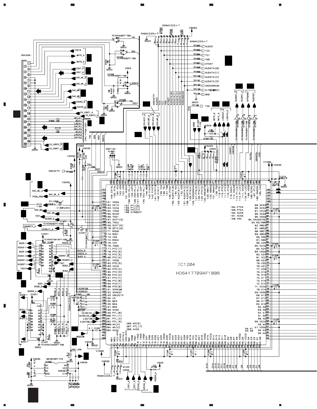
MAIN ASSY
3/3
A
CMX-3000, CU-V163
31
Page 32

CMX-3000, CU-V163
Voltage (1/3)
IC1200 (DYW1701)
Pin No. Voltage (V)
1 0 to 3.2
2 0 to 3.2
3 0 to 3.2
4 0 to 3.2
5 0 to 3.2
6 0 to 3.2
7 0 to 3.2
8 0 to 3.2
9 0 to 3.2
10 0.7
11 0.7
12 0 to 3.2
13 0.7
14 0.7
15 3.1
16 0 to 3.2
17 0 to 3.2
18 0 to 3.2
19 0 to 3.2
20 0 to 3.2
21 0 to 3.2
22 0 to 3.2
23 0 to 3.2
24 0 to 3.2
25 0 to 3.2
26 3.2
27 0
28 0 to 3.2
29 0 to 3.2
30 0 to 3.2
31 0 to 3.2
32 0 to 3.2
33 0 to 3.2
34 0 to 3.2
35 0 to 3.2
36 0 to 3.2
37 3.1
38 0 to 3.2
39 0 to 3.2
40 0 to 3.2
41 0 to 3.2
42 0 to 3.2
43 0 to 3.2
44 0 to 3.2
45 0 to 3.2
46 0
47 3.1
48 0 to 3.2
IC1022 (M51957BFP)
Pin No. Voltage (V)
1 0
2 0
3 0
4 0
5 1.3
6 3.2
7 3.2
8 0
A
1/3
MAIN ASSY
IC1204 (HD6417709AF100B)
Pin No. Voltage (V)
1 3.2
2 0
3 1.8
4 1.6
5 0
6 0
7 0
8 0
9 0
10 3.3
11 3.2
12 3.3
13 0 to 3.3
14 0
15 0
16 0
17 3.3
18 3.3
19 0
20 0
21 3.3
22 0
23 0
24 0
25 0
26 0
27 0
28 0
29 1.8
30 0
31 0
32 0
33 0
34 0 to 3.3
35 3.2
36 0 to 3.3
37 0 to 3.3
38 0 to 3.3
39 0 to 3.3
40 0 to 3.3
41 0 to 3.3
42 0 to 3.3
43 0 to 3.3
44 0 to 3.3
45 0
46 0 to 3.3
47 3.3
48 0 to 3.3
49 0 to 3.3
50 0 to 3.3
51 0 to 3.3
52 0 to 3.3
53 0 to 3.3
54 0 to 3.3
55 0 to 3.3
56 0 to 3.3
57 0
58 0 to 3.3
59 3.3
60 0 to 3.3
61 0 to 3.3
62 0 to 3.3
63 0 to 3.3
64 0 to 3.3
65 0 to 3.3
66 0 to 3.3
67 0 to 3.3
68 0 to 3.3
69 0
70 0 to 3.3
71 3.3
72 0 to 3.3
73 0 to 3.3
74 0 to 3.3
75 0 to 3.3
76 0 to 3.3
77 0 to 3.3
78 0 to 3.3
79 0
80 0
81 1.8
82 0 to 3.3
83 0
84 0 to 3.3
85 3.3
86 0 to 3.3
87 3.2
88 0 to 3.3
89 0 to 3.3
90 0 to 3.3
Pin No. Voltage (V)
91 3.2
92 3.2
93 0 to 3.3
94 3.2
95 0
96 3.3
97 3.3
98 0 to 3.3
99 0 to 3.3
100 0 to 3.3
101 3.2
102 3.2
103 3.2
104 3.2
105 3.2
106 0 to 3.3
107 0 to 3.3
108 0 to 3.3
109 0
110 0
111 3.2
112 0
113 0
114 0 to 3.3
115 0 to 3.3
116 3.2
117 3.2
118 0
119 0
120 3.3
121 3.2
122 3.2
123 3.2
124 3.2
125 3.2
126 3.1
127 3
128 3.2
129 2.8
130 0
131 0
132 0
133 3.2
134 1.8
135 3.2
136 3.0
137 3.0
138 3.0
139 3.0
140 3.1
141 0
142 3.0
143 0
144 0
145 1.8
146 0.7
147 0
148 0
149 0.7
150 1.8
151 1.9
152 0
153 0
154 1.8
155 1.6
156 1.1
157 3.2
158 3.2
159 3.2
160 0 to 3.2
161 0
162 0 to 3.2
163 3.2
164 0
165 3.2
166 3.2
167 0 to 3.2
168 0 to 3.2
169 0
170 0
171 3.2
172 3.2
173 0
174 0 to 3.2
175 1.8
176 3.0
177 0 to 3.2
178 0 to 3.2
179 0 to 3.2
180 0 to 3.2
Pin No. Voltage (V)
181 0
182 0 to 3.2
183 3.2
184 0 to 3.2
185 0 to 3.2
186 0 to 3.2
187 0 to 3.2
188 0 to 3.2
189 0 to 3.2
190 0 to 3.2
191 0 to 3.2
192 0 to 3.2
193 3.2
194 3.1
195 0
196 3.1
197 0
198 0
199 3.0
200 3.0
201 3.2
202 3.2
203 3.1
204 0
205 3.2
206 0.7
207 0.7
208 0
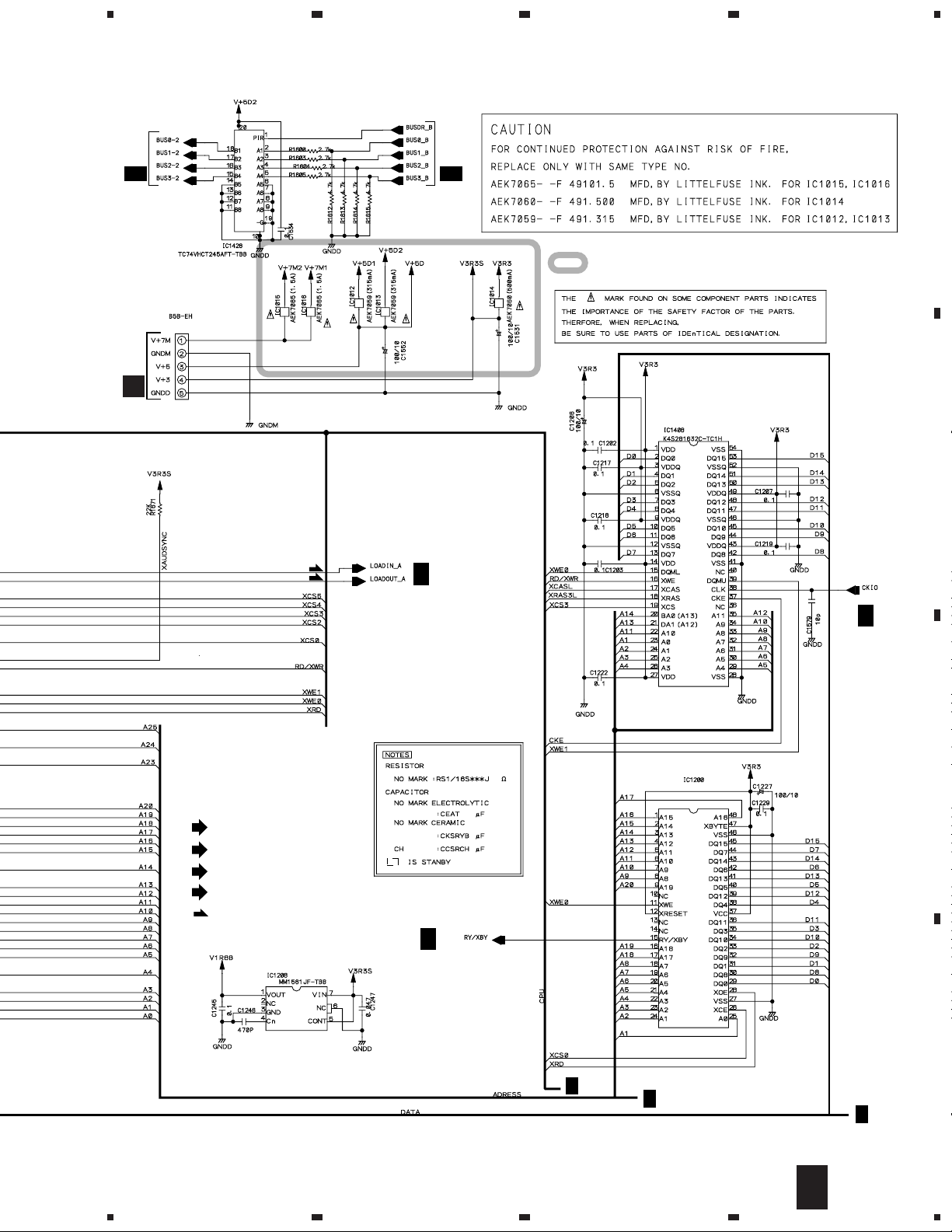
IC1408 (K4S281632)
Pin No. Voltage (V)
1 3.2
2 0 to 3.3
3 3.2
4 0 to 3.3
5 0 to 3.3
6 0
7 0 to 3.3
8 0 to 3.3
9 3.2
10 0 to 3.3
11 0 to 3.3
12 0
13 0 to 3.3
14 3.2
15 0 to 3.3
16 0 to 3.3
17 0 to 3.3
18 0 to 3.3
19 0 to 3.3
20 0 to 3.3
21 0 to 3.3
22 0 to 3.3
23 0 to 3.3
24 0 to 3.3
25 0 to 3.3
26 0 to 3.3
27 3.2
28 0
29 0 to 3.3
30 0 to 3.3
31 0 to 3.3
32 0 to 3.3
33 0 to 3.3
34 0 to 3.3
35 0 to 3.3
36 0
37 3.2
38 0 to 3.3
39 0 to 3.3
40 0.7
41 0
42 0 to 3.3
43 3.2
44 0 to 3.3
45 0 to 3.3
46 0
47 0 to 3.3
48 0 to 3.3
49 3.2
50 0.7
51 0 to 3.3
52 0
53 0 to 3.3
54 0
32
Page 33

Voltage (2/3)
IC1402 (XCA56367PV150)
Pin No. Voltage (V)
1 1.1
2 0.7
3 0.6
4 0 to 3.2
5 0 to 3.2
6 0 to 3.2
7 0 to 3.2
8 3.2
9 0
10 0 to 3.2
11 0 to 3.2
12 0 to 3.2
13 0 to 3.2
14 0
15 0 to 3.2
16 0 to 3.2
17 0 to 3.2
18 1.8
19 0
20 3.3
21 0 to 3.2
22 0 to 3.2
23 0 to 3.2
24 0
25 3.2
26 0
27 0
28 0.7
29 0
30 3.2
31 3.2
32 0.8
33 0 to 3.2
34 0 to 3.2
35 0 to 3.2
36 0 to 3.2
37 0 to 3.2
38 3.2
39 0
40 0 to 3.2
41 0 to 3.2
42 0 to 3.2
43 0 to 3.2
44 3.2
45 1.8
46 0.9
47 0
48 0 to 3.2
49 3.2
50 0 to 3.2
51 0.9
52 0.7
53 3.2
54 0 to 3.2
55 0
56 0 to 3.4
57 1.8
58 0
59 0 to 3.2
60 0 to 3.2
61 0.7
62 0
63 3.2
64 3.1
65 3.2
66 0
67 0.7
68 0.7
69 0.7
70 0.7
71 0
72 0.7
73 0
74 3.2
75 0
76 0
77 0
78 0
79 0
80 3.2
81 0
82 0
83 0
84 0
85 0
86 3.2
87 0
88 0
89 0
90 0
Pin No. Voltage (V)
91 1.8
92 0
93 0
94 0
95 3.2
96 0
97 0
98 0
99 0
100 0
101 0
102 0
103 3.2
104 0
105 0
106 0
107 0
108 0
109 0
110 0
111 3.2
112 0
113 0
114 0.6
115 0.6
116 0
117 0
118 0.6
119 0.7
120 0.7
121 0
122 0
123 0
124 0
125 0
126 0
127 0
128 0
129 3.2
130 0
131 0
132 0
133 0
134 2.6
135 0
136 0
137 0
138 1 to 3.2
139 0
140 0
141 0
142 0
143 0
144 0.6
A
2/3
MAIN ASSY
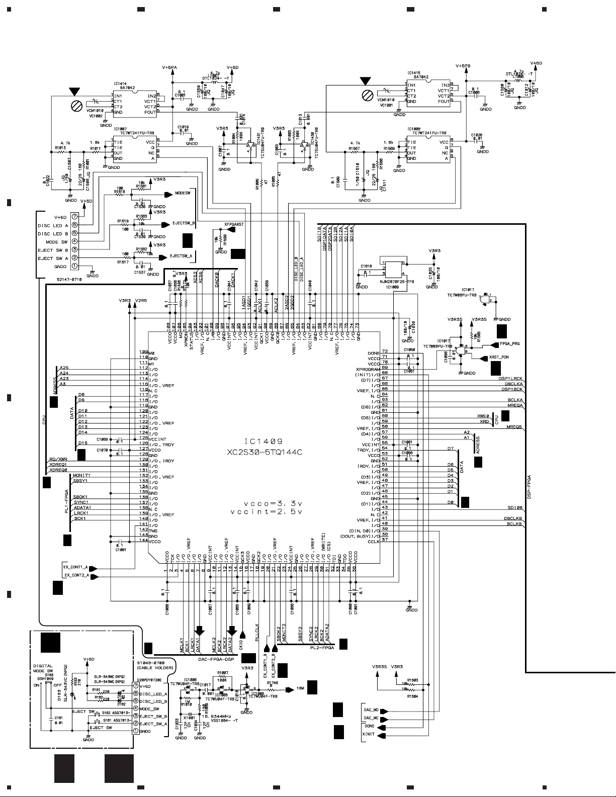
IC1409 (XC2S30-5TQ144C)
Pin No. Voltage (V)
1 3.2
2 2.4
3 3.1
4 0.4 to 2.1
5 0 to 3.1
6 0 to 3.1
7 0 to 3.1
8 0
9 0
10 0.4 to 2.9
11 0 to 3.1
12 0 to 3.1
13 0 to 3.1
14 2.5
15 0 to 3.1
16 0.7
17 0.6
18 0.6
19 0.6
20 0.6
21 3.2
22 0.6
23 0 to 4.9
24 2.5
25 0.6
26 0.6
27 0
28 0 to 4.9
29 0 to 4.9
30 11 to 3.8
31 0 to 4.9
32 2.4
33 0.6
34 0.6
35 3.2
36 0.6
37 3.2
38 0
39 0
40 0 to 3.0
41 0 to 3.2
42 0
43 0 to 3.2
44 0 to 3.2
45 0
46 0 to 3.2
47 0 to 3.2
48 0 to 3.2
49 0 to 3.2
50 0 to 3.2
51 0 to 3.2
52 0
53 3.2
54 0 to 3.2
55 2.5
56 0 to 3.2
57 0 to 3.2
58 0 to 3.2
59 0 to 3.2
60 0 to 3.2
61 0
62 0
63 0 to 3.0
64 0
65 0 to 3.0
66 0 to 3.1
67 2.9
68 2.9
69 3.2
70 3.2
71 3.2
72 3.2
73 0
74 0 to 3.1
75 0 to 3.1
76 0 to 3.1
77 0.6
78 0 to 3.1
79 0 to 3.1
80 0 to 3.1
81 0
82 2.5
83 0.6
84 0
85 0
86 3.2
87 0
88 0.7 to 2.6
89 0
90 0.6
Pin No. Voltage (V)
91 0
92 2.5
93 0
94 3.2
95 0
96 0 to 3.2
97 2.5
98 0
99 0 to 3.2
100 3.2
101 0
102 3.2
103 0 to 3.2
104 0.6
105 0.6
106 0
107 3.2
108 3.2
109 2.5
110 0
111 2.5
112 0 to 3.2
113 0 to 3.2
114 0 to 3.2
115 0 to 3.2
116 0
117 0 to 3.2
118 0 to 3.2
119 0
120 0 to 3.2
121 0 to 3.2
122 0 to 3.2
123 0 to 3.2
124 0 to 3.2
125 0.6
126 3.2
127 0
128 0.7
129 0.7
130 0 to 3.2
131 0 to 3.2
132 0 to 4.9
133 0.7
134 0
135 0
136 0 to 4.9
137 0 to 4.9
138 0 to 4.9
139 0 to 4.9
140 1 to 3.8
141 3.2
142 2.4
143 0
144 3.2
CMX-3000, CU-V163
IC1414 (BA7042)
Pin No. Voltage (V)
1 0
2 2.3
3 0
4 0
5 2.5 to 4.5
6 5.0
7 2.6
8 2.6
33
Page 34

CMX-3000, CU-V163
Voltage (3/3)
A
3/3
MAIN ASSY
IC1005 (TC9495F)
Pin No. Voltage (V)
1 4.4
2 0
3 5.0
4 0
5 0 to 4.9
6 0
7 0.3 to 4.4
8 0 to 4.9
9 0
10 0
11 0
12 5.0
13 0 to 4.2
14 5.0
15 0
16 0 to 4.9
17 0 to 4.9
18 0 to 4.9
19 0.3 to 4.2
20 0 to 4.7
21 0 to 4.9
22 0 to 4.5
23 4.9
24 0
25 4.2
26 2.1
27 0 to 4.9
28 5.0
29 0
30 4.2
31 2.1
32 2.0
33 2.1
34 2.1
35 1.3
36 0
37 2.1
38 1.6 to 2.6
39 5.0
40 3.0
41 3.1
42 2.5 to 2.9
43 2.5 to 2.9
44 2.5
45 2.1
46 1.4 to 2.9
47 0 to 4.1
48 0.7 to 2.2
49 1.4 to 3.4
50 2.1
51 0.4 to 2.1
52 2.1
53 0.4 to 2.1
54 2.1
55 0 to 4.2
56 4.2
57 2.1
58 0 to 5.0
59 5.0
60 5.0
61 0
62 5.0
63 0
64 5.0
65 0
66 0
67 0 to 5.0
68 4.9
69 4.9
70 4.9
71 0
72 0
73 0
74 0
75 5.0
76 5.0
77 0
78 1.0 to 3.0
79 0.5 to 4.5
80 5.0
81 0
82 0.4
83 0
84 0
85 0.4
86 0
87 4.8
88 4.8
89 4.8
90 0 to 5.0
Pin No. Voltage (V)
91 0 to 5.0
92 0 to 5.0
93 0 to 5.0
94 5.0
95 0
96 5.0
97 0 to 5.0
98 4.7
99 4.7
100 5.0
IC1010 (TA2153FN)
Pin No. Voltage (V)
1 4.9
2 1.8
3 2.1
4 2.1
5 2.1
6 2.0
7 2.1
8 0
9 4.3
10 0
11 2.1
12 4.1
13 2.1
14 2.1
15 1.2
16 2.1
17 2.1
18 0.0
19 2.1
20 1.1
21 1.8
22 1.1
23 0.5
24 2.0
25 2.1
26 0
27 2.2
28 1.0 to 2.1
29 0
30 2.1
IC1011(LA6562)
Pin No. Voltage (V)
1 4.3
2 4.3
3 7.3
4 3.3
5 3.3
6 3.4
7 3.2
8 2.5
9 3.5
10 0
11 3.7
12 3.4
13 3.8
14 3.7
15 7.3
16 2.0
17 2.0
18 2.0
19 2.0
20 2.0
21 2.0
22 2.0
23 2.0
24 2.0
25 1.0
26 0.6
27 1.0
28 2.0
29 0
30 2.0
31 2.0
32 2.0
33 2.0
34 2.5
35 2.5
36 2.0
37 0
38 3.2
IC201 (PE8001)
Pin No. Voltage (V)
1 0 to 3.1
2 0 to 3.1
3 0 to 3.1
4 0.3 to 4.4
5 0.5 to 2.7
6 0.8 to 4.8
7 0
8 5.0
9 5.0
10 0
11 0 to 2.5
12 0
13 2.5
14 0
15 5.0
16 2.2
17 0.7
18 0
19 0
20 5.0
21 3.0
22 0
23 0
24 0
25 0 to 4.9
26 0
27 0.5
28 3.2
IC301 (PD5764A)
Pin No. Voltage (V)
1 0
2 0
3 0
4 0
5 5.0
6 5.0
7 0
8 0
9 0
10 0 to 5.0
11 0 to 5.0
12 0 to 5.0
13 0 to 5.0
14 0 to 5.0
15 0 to 5.0
16 0 to 5.0
17 0
18 5.0
19 0 to 5.0
20 0 to 5.0
21 0
22 0 to 4.3
23 0 to 5.0
24 5.0
25 0
26 0
27 0
28 0
29 0 to 5.0
30 0 to 5.0
31 0 to 5.0
32 0 to 5.0
33 5.0
34 5.0
35 5.0
36 5.0
37 -31 to 5.0
38 -31 to 5.0
39 -31 to 5.0
40 -31 to 5.0
41 -31 to 5.0
42 -31 to 5.0
43 -31 to 5.0
44 -31 to 5.0
45 -31 to 5.0
46 -31 to 5.0
47 -31 to 5.0
48 -31 to 5.0
49 -31 to 5.0
50 -31 to 5.0
JACB ASSY
E
CNTA ASSY
I
Pin No. Voltage (V)
IC211 (NJM2360M)
Pin No. Voltage (V)
1 7.1
2 0 to 5.6
3 -7.5
4 -7.9
5 0.5
6 6.9
7 6.9
8 6.9
51 -31 to 5.0
52 -31 to 5.0
53 -31 to 5.0
54 -31 to 5.0
55 -31 to 5.0
56 -31 to 5.0
57 -31 to 5.0
58 -31 to 5.0
59 -31 to 5.0
60 -31 to 5.0
61 -31 to 5.0
62 -31 to 5.0
63 -31 to 5.0
64 -31 to 5.0
65 -31 to 5.0
66 -31 to 5.0
67 -31 to 5.0
68 -31 to 5.0
69 -31 to 5.0
70 -31 to 5.0
71 -31 to 5.0
72 -31 to 5.0
73 -31
74 -31
75 -31
76 -31 to 5.0
77 -31 to 5.0
78 -31 to 5.0
79 -31 to 5.0
80 -31 to 5.0
81 -31 to 5.0
82 -31 to 5.0
83 -31 to 5.0
84 -31 to 5.0
85 -31 to 5.0
86 -31 to 5.0
87 -31 to 5.0
88 -31 to 5.0
89 -31
90 0 to 5.0
91 0 to 5.0
92 0 to 5.0
93 1.3
94 0 to 5.0
95 0 to 5.0
96 0
97 0
98 5.0
99 2.5
100 0 to 5.0
IC501 (PD5764A)
Pin No. Voltage (V)
1 5.0
2 5.0
3 5.0
4 5.0
5 5.0
6 5.0
7 0 to 5.0
8 0 to 5.0
9 0
10 0 to 5.0
11 0 to 5.0
12 0 to 5.0
13 0 to 5.0
14 0 to 5.0
15 0
16 0
17 0
18 5.0
19 0
20 0
21 0
22 0 to 4.0
23 0 to 5.0
24 0 to 5.0
25 5.0
26 0 to 5.0
27 0 to 5.0
28 0 to 5.0
29 0 to 5.0
30 0 to 5.0
31 0 to 5.0
32 0 to 5.0
33 5.0
34 5.0
35 0 to 5.0
36 0 to 5.0
37 -31 to 5.0
38 -31 to 5.0
39 -31 to 5.0
40 -31 to 5.0
41 -31 to 5.0
42 -31 to 5.0
43 -31 to 5.0
44 -31 to 5.0
45 -31 to 5.0
46 -31 to 5.0
47 -31 to 5.0
48 -31 to 5.0
49 -31 to 5.0
50 -31 to 5.0
CNTB ASSY
K
Pin No. Voltage (V)
51 -31 to 5.0
52 -31 to 5.0
53 -31 to 5.0
54 -31 to 5.0
55 -31 to 5.0
56 -31 to 5.0
57 -31 to 5.0
58 -31 to 5.0
59 -31 to 5.0
60 -31 to 5.0
61 -31 to 5.0
62 -31 to 5.0
63 -31 to 5.0
64 -31 to 5.0
65 -31 to 5.0
66 -31 to 5.0
67 -31 to 5.0
68 -31 to 5.0
69 -31 to 5.0
70 -31 to 5.0
71 -31 to 5.0
72 -31 to 5.0
73 -31
74 -31
75 -31
76 -31 to 5.0
77 -31 to 5.0
78 -31 to 5.0
79 -31 to 5.0
80 -31 to 5.0
81 -31 to 5.0
82 -31 to 5.0
83 -31 to 5.0
84 -31 to 5.0
85 -31 to 5.0
86 -31 to 5.0
87 -31 to 5.0
88 -31 to 5.0
89 -31
90 0 to 5.0
91 0 to 5.0
92 0 to 5.0
93 5.0
94 0 to 5.0
95 0 to 5.0
96 5.0
97 0
98 5.0
99 2.5
100 0 to 5.0
34
Page 35

4. PCB CONNECTION DIAGRAM
NOTE FOR PCB DIAGRAMS :
1. Part numbers in PCB diagrams match those in the schematic
diagrams.
2. A comparison between the main parts of PCB and schematic
diagrams is shown below.
Symbol In PCB
Diagrams
BCE
BCE
Symbol In Schematic
Diagrams
BCEBCE
BCE
BCE
Part Name
Transistor
Transistor
with resistor
CMX-3000, CU-V163
3. The parts mounted on this PCB include all necessary parts for
several destinations.
For further information for respective destinations, be sure to
check with the schematic diagram.
4. View point of PCB diagrams.
Connector
Capacitor
SIDE A
DGGSS
D
DGS
Field effect
transistor
Resistor array
3-terminal
regulator
P.C.Board
Chip Part
SIDE B
35
Page 36

1
234
CMX-3000, CU-V163
4.1 MAIN, FRSW, SLM1 and SLM2 ASSYS
A
SLM1 ASSY
C
FRSW ASSY
B
SIDE A
(DNP2002-C)
To Slot Mecha (A)
pick up Assy (CN1)
MAIN ASSY
B
A
CN1012
A
(DNP2002-C)
CN201
E
To Slot Mecha (A) Loading Motor (J4)To Slot Mecha (A) Servo Mecha
C
D
(DNP2003-B)
IC1011
IC1445
IC1448IC1447
IC1005
IC1010
Q1003
Q1002
IC1428
IC1013
IC1006
IC1409
IC1408
IC1406
IC1015 IC1012
B
J161
IC1415 IC1414
IC1431IC1430IC1008 IC1007
36
A B C
1234
Page 37

5
67
8
CMX-3000, CU-V163
A
SLM2 ASSY
D
201
(DNP2002-C)
To Slot Mecha (B)
Servo Mecha
To Slot Mecha (B)
Loading Motor (J4)
SIDE A
To Slot Mecha (B)
pick up Assy (CN1)
B
C
D
IC1450
IC1002
Q1229
IC1003
DA
8
Q1228
37
IC1208IC1001IC1440
IC1204IC1408
7
IC1200
IC1009 IC1014 IC1427IC1022IC1017
5
CN104
F
6
IC1437 IC1444
IC1016
7
IC1004
IC1443
Page 38

1
CMX-3000, CU-V163
A
SIDE B
MAIN ASSY
A
B
MAIN ASSY
A
234
C
D
38
A
1234
Page 39

5
67
8
CMX-3000, CU-V163
A
SIDE B
B
C
(DNP2003)
D
5
6
7
8
A
39
Page 40

1
CMX-3000, CU-V163
4.2 PWRB, REGB and ACIN ASSYS
A
REGB ASSY
H
(DNP2002-C)
SIDE A
F
B
234
CN1218
A
PWRB ASSY
IC103
IC104
IC106IC101
C
ACIN ASSY
G
D
(DNP2002-C)
40
F
ACIN
G
1234
H
(DNP2002-C)
Page 41

1
23
4
CMX-3000, CU-V163
A
JACB ASSY
E
JA701
M
IC209
IC212
IC210
IC207
SIDE A
IC213
Q171
Q215
B
C
(DNP2002-C)
1
D
2
3
4
E
41
Page 42

1
CMX-3000, CU-V163
JACB ASSY
E
A
IC172
SIDE B
B
234
Q213
Q214
Q201
Q202
Q208
C
Q206
Q207
IC201IC204
Q205
Q212
Q211
D
42
E
IC205 IC202
Q209
Q210
1234
Q203
Q204
(DNP2002-C)
Page 43

1
23
4
CMX-3000, CU-V163
REGB ASSY
H
A
(DNP2002-C)
SIDE B
PWRB ASSY
F
B
C
D
(DNP2002-C)
F
1
2
3
H
4
43
Page 44

1
CMX-3000, CU-V163
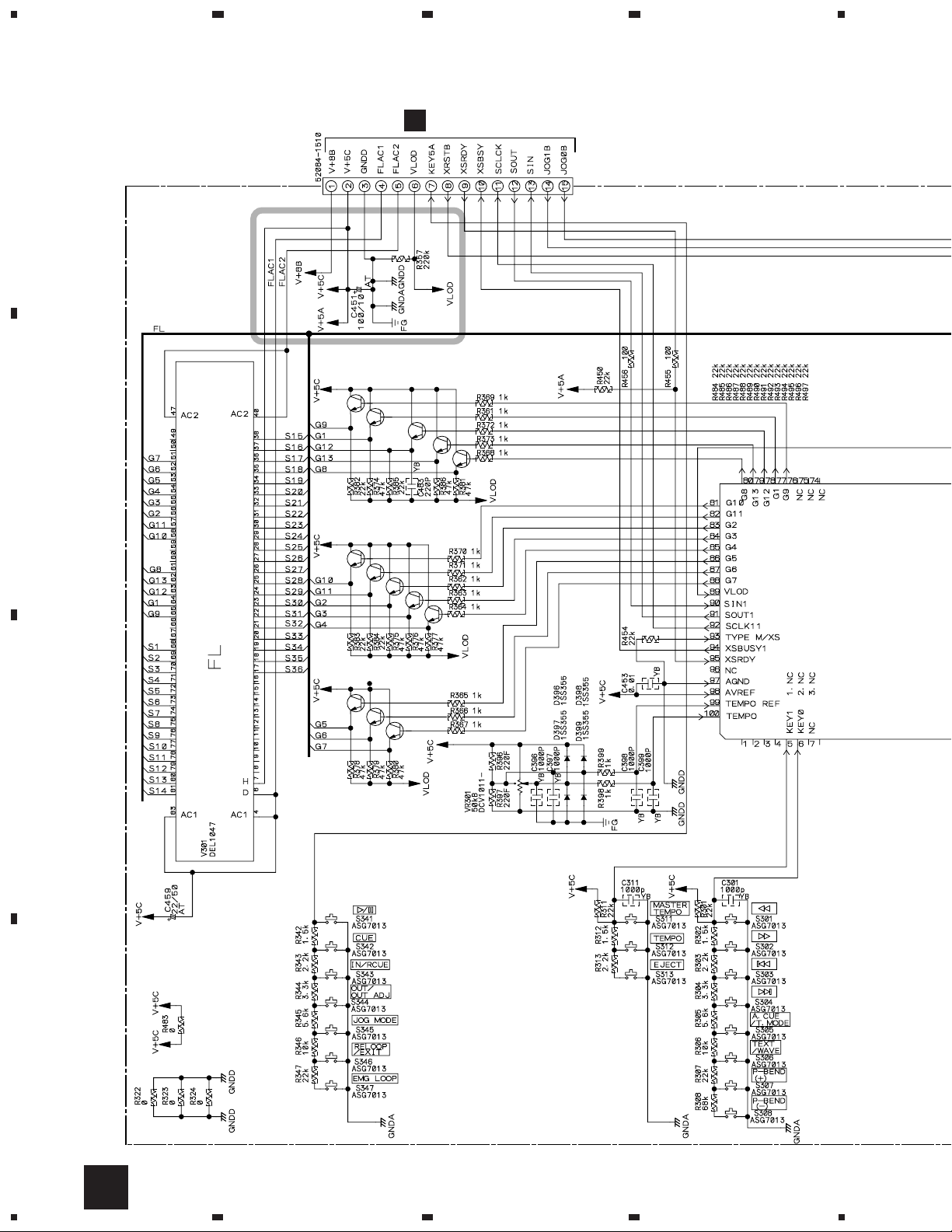
4.3 CNTA and PHTA ASSYS
A
234
I
CNTA ASSY
SIDE A
B
J
PHTA ASSY
C
(DNP2004-B)
CN702
M
D
(DNP2004-B)
44
I
SWITCHES FUNCTION
S301 : 1
S302 : ¡
S303 : 4
S304 : ¢
S305 : AUTO CUE/ TIME MODE
S306 : TEXT/ WAVE
S307 : PITCH BEND [ + ]
S308 : PITCH BEND [ - ]
S311 : MASTER TEMPO
S312 : TEMPO
S313 : 0 (EJECT)
S341 : 6
S342 : CUE
S343 : IN/REALTIME CUE
S344 : OUT/ OUT ADJ
S345 : JOG MODE
S346 : RELOOP/ EXIT
S347 : EMERGENCY LOOP
J
1234
Page 45

1
I
CNTA ASSY
SIDE B
23
CMX-3000, CU-V163
4
A
J
PHTA ASSY
(DNP2004-B)
B
C
D
Q369
Q408
Q409
1
IC305Q410
2
IC304
IC303
Q368
Q361 Q370
Q372
Q371
Q373 Q362
Q406 Q403 Q404
Q363
Q364
Q365
Q366
Q367
IC301
(DNP2004-B)
I
3
J
4
45
Page 46

1
H
CMX-3000, CU-V163
4.4 CNTB and PHTB ASSYS
A
SIDE A
234
P
L
CNTB ASSY
K
(DNP2002-B)
B
C
SWITCHES FINCTION
S501 : 1
S502 : ¡
S503 : 4
S504 : ¢
S505 :
AUTO CUE/ TIME MODE
S506 : TEXT/ WAVE
S507 : PITCH BEND [ + ]
S508 : PITCH BEND [ - ]
D
46
K
1234
S511 : MASTER TEMPO
S512 : TEMPO RANGE
S513 : 0 (EJECT)
S514 : BPM SYNC
S515 : RELAY PLAY
S521 : HOT CUE 1 - B
S522 : HOT CUE 2 - B
S523 : HOT CUE 3 - B
S524 : HOT CUE REC - B
S525 : BPM AUTO - B
S526 : BPM TAP - B
S531 : HOT CUE 1 - A
S532 : HOT CUE 2 - A
S533 : HOT CUE 3 - A
S534 : HOT CUE REC - A
S535 : BPM AUTO - A
S536 : BPM TAP - A
S541 : 6
S542 : CUE
S543 : IN/ REALTIME CUE
S544 : OUT/ OUT ADJ
S545 : JOG MODE
S546 : RELOOP/ EXIT
S547 : EMERGENCY LOOP
Page 47

P2002-B)
PHTB ASSY
L
5
67
8
CMX-3000, CU-V163
A
SIDE A
B
C
IC502
5
6
(DNP2002-B)
D
7
K
L
8
47
Page 48

1
CMX-3000, CU-V163
4.5 CNTB, PHTB and CNNB ASSYS
A
PHTB ASSY
L
SIDE B
234
CNNB ASSY
M
SIDE A
B
C
CNTB ASSY
K
(DNP2004-B)
D
(DNP2004-B)
48
K
1234
L
M
Q569Q561Q572Q573
Q568Q570Q571Q562
Q563IC501 Q564Q565Q566Q567
Q608Q609
Q60IC503
Page 49

5
IC701
E
67
CMX-3000, CU-V163
JA207
(DNP2004-B)
SIDE A
I
8
A
CN303
B
SIDE B
C
Q606 Q615 Q611
Q603
Q604
Q616
Q618
5
Q601Q602
Q612
Q613Q614Q617
6
D
7
K
M
8
49
Page 50

CMX-3000, CU-V163
5. PCB PARTS LIST
NOTES:•Parts marked by "NSP" are generally unavailable because they are not in our Master Spare Parts List.
• LIST OF WHOLE PCB ASSEMBLIES (FOR CMX-3000)
Mark
NSP POWB ASSY DWM2130 DWM2127 DWM2131
1: Although DWR1357 and DWR 1347 are different in part number, they consist of the same components.
*
2: Although DWX2214 and DWX2200 are different in part number, they consist of the same components.
*
The mark found on some component parts indicates the importance of the safety factor of the part.
•
Therefore, when replacing, be sure to use parts of identical designation.
When ordering resistors, first convert resistance values into code form as shown in the following examples.
•
Ex.1 When there are 2 effective digits (any digit apart from 0), such as 560 ohm and 47k ohm (tolerance is shown by J=5%,
and K=10%).
560 Ω→56 × 10
47k Ω→47 × 10
0.5 Ω→R50 ..................................................................................... RN2H
1 Ω→1R0 ..................................................................................... RS1P 1 R 0 K
Ex.2 When there are 3 effective digits (such as in high precision metal film resistors).
5.62k Ω→ 562 × 10
Symbol and Description
MAIN ASSY DWG1556 DWG1556 DWG1556
PWRB ASSY DWR1345 DWR1345 DWR1348
ACIN ASSY DWR1349 DWR1346 DWR1346
REGB ASSY DWR1357 DWR1347 DWR1347
FRSW ASSY DWS1314 DWS1314 DWS1314
SLM1 ASSY DWS1315 DWS1315 DWS1315
SLM2 ASSY DWS1316 DWS1316 DWS1316
JACB ASSY DWX2214 DWX2200 DWX2200
1
→ 561 ........................................................ RD1/4PU 5 6 1 J
3
→ 473 ........................................................ RD1/4PU 4 7 3 J
R 5 0
1
→ 5621 ...................................................... RN1/4PC 5 6 2 1 F
Part No.
CMX-3000/
KUCXJ
CMX-3000/
WYXJ
CMX-3000/
RLBXJ
K
1
*
2
*
Remarks
• LIST OF PCB ASSEMBLIES (FOR CU-V163)
NSP CONT ASSY DWM2129
CNTA ASSY DWG1551
CNTB ASSY DWG1552
CNNB ASSY DWG1553
PHTA ASSY DWG1554
PHTB ASSY DWG1555
• CONTRAST OF PCB ASSEMBLIES
PWRB ASSY
F
DWR1345 and DWR1348 are constructed the same except for the following:
Mark
ACIN ASSY
H
Symbol and Description
DWR1345 DWR1348
S105 (Voltage Selector) Not used DSA1026
DWR1349 and DWR1346 are constructed the same except for the following:
Mark
Symbol and Description
DWR1349 DWR1346
AN101 (Power Socket) AKP7032 Not used
AN101 (1P AC Inlet) Not used BKP1046
Part No.
Part No.
Remarks
Remarks
50
Page 51

CMX-3000, CU-V163
• PARTS LIST FOR CMX-3000/ KUCXJ
Mark No. Description Part No. Mark No. Description Part No.
MAIN ASSY
A
SEMICONDUCTORS
IC1012, IC1013 (315 mA) AEK7059
IC1014 (500 mA) AEK7060
IC1015, IC1016 (1.5 A) AEK7065
IC1414, IC1415 BA7042
IC1200 DYW1701
IC1204 HD6417709AF100B
IC1408 K4S281632C-TC1H
IC1004, IC1011 LA6562
IC1022 M51957BFP
IC1208 MM1561JF
IC1444, IC1445, IC1448, IC1450 NJM2100M
IC1406 NJM2870F18
IC1009 NJM2870F25
IC1443, IC1447 NJM2903M
IC1003, IC1010 TA2153FN
IC1440 TC74VHC02FT
IC1437 TC74VHC04FT
IC1427, IC1428 TC74VHCT245AFT
IC1001 TC74VHCT541AFT
IC1430, IC1431 TC7SU04FU
IC1017 TC7W08FU
IC1007, IC1008 TC7WT241FU
IC1006 TC7WU04FU
IC1002, IC1005 TC9495F
IC1409 XC2S30-5TQ144C
IC1402 XCA56367PV150
Q 1003, Q 1229 2SA1036K
Q 1002, Q 1228 DTC114TK
D1202, D1203 UDZ2.0B
COILS AND FILTERS
L1004, L1006, L1007, L1009 DTL1024
F1001, F1002 DTL1090
L1021, L1022 LCYAR68J2520
CAPACITORS
C1117, C1174, C1579, C1582, C1593 CCSRCH100D50
C1104, C1106, C1166, C1168, C1404 CCSRCH101J50
C1421, C1424, C1430, C1435 CCSRCH101J50
C1033, C1034 CCSRCH120J50
C1581, C1592 CCSRCH121J50
C1587, C1588, C1597, C1599 CCSRCH180J50
C1121, C1178 CCSRCH270J50
C1099, C1100, C1164, C1165 CCSRCH330J50
C1064, C1128, C1149, C1186 CCSRCH470J50
C1074, C1156, C1616, C1617 CCSRCH471J50
C1107, C1169 CCSRCK2R0C50
C1004, C1006, C1009, C1024 CEAT101M10
C1035, C1036, C1093, C1105, C1124 CEAT101M10
C1135, C1137, C1161, C1167, C1181 CEAT101M10
C1192, C1194, C1206, C1215, C1216 CEAT101M10
C1227, C1410, C1413, C1453, C1531 CEAT101M10
C1552 CEAT101M10
C1132, C1189 CEAT221M10
C1012, C1047, C1559, C1560 CEJQ101M6R3
C1507, C1510 CEJQ1R0M50
C1508, C1511 CEJQ220M25
C1013, C1014, C1017 CKSRYB102K50
C1010, C1015, C1019, C1020, C1023 CKSRYB103K50
C1025, C1026, C1029, C1032 CKSRYB103K50
C1044-C1046, C1048, C1055, C1065 CKSRYB103K50
C1071, C1094, C1095, C1098 CKSRYB103K50
C1108-C1111, C1118, C1127, C1136 CKSRYB103K50
C1139, C1142-C1144, C1150, C1151 CKSRYB103K50
C1154, C1162, C1163, C1175, C1185 CKSRYB103K50
C1193, C1196, C1401-C1403 CKSRYB103K50
C1405-C1408, C1417, C1422, C1423 CKSRYB103K50
C1426-C1428, C1431-C1434, C1436 CKSRYB103K50
C1486, C1512, C1533, C1534 CKSRYB103K50
C1536, C1537, C1539, C1554 CKSRYB103K50
C1561-C1564, C1577, C1578 CKSRYB103K50
C1583-C1585, C1589, C1590 CKSRYB103K50
C1594-C1596, C1598, C1601, C1603 CKSRYB103K50
C1606, C1608-C1615, C1619, C1620 CKSRYB103K50
C1001, C1003, C1007, C1008, C1018 CKSRYB104K25
C1022, C1037-C1042, C1050, C1051 CKSRYB104K25
C1056, C1061, C1069, C1070, C1081 CKSRYB104K25
C1085-C1091, C1113, C1114, C1129 CKSRYB104K25
C1133, C1138, C1140, C1170, C1171 CKSRYB104K25
C1183, C1190, C1195, C1197 CKSRYB104K25
C1202, C1203, C1207-C1209 CKSRYB104K25
C1212-C1214, C1217-C1224, C1226 CKSRYB104K25
C1228-C1234, C1236-C1239, C1245 CKSRYB104K25
C1509, C1618 CKSRYB104K25
C1066, C1152 CKSRYB153K50
C1072, C1155 CKSRYB222K50
C1115, C1116, C1172, C1173 CKSRYB224K16
C1429 CKSRYB332K50
C1078, C1157 CKSRYB333K16
C1210, C1211, C1246 CKSRYB471K50
C1080, C1083, C1158, C1159, C1247 CKSRYB473K50
C1487 CKSRYB473K50
C1119, C1176 CKSRYB562K50
VC1001, VC1002 (40P) VCM1010
RESISTORS
R1202-R1204, R1221, R1223 RAB4C223J
R 1401,R 1402,R 1409,R 1413,R 1418 RAB4C223J
R 1425,R 1426,R 1584,R 1585,R 1594 RAB4C223J
R1086 RN1/16SE3301D
R1085 RN1/16SE4701D
R1711, R1715 RS1/16S1502F
R1703, R1704, R1721, R1723 RS1/16S3301F
R1706, R1707, R1719, R1720 RS1/16S3902F
R1710, R1716 RS1/16S4701F
R1705, R1722 RS1/16S5600F
R1708, R1709, R1717, R1718 RS1/16S8202F
Other Resistors RS1/16S&&& J
OTHERS
CN1005, CN1009 FPC CONNECTOR 16FMZ-ST
CN1012 7P JUMPER CONNECTOR 52147-0710
CN1004, CN1008 CONNECTOR POST B2B-PH-K-S
CN1002, CN1006 CONNECTOR POST B3B-PH-K-S
CN1218 5P TOP POST B5B-EH
51
Page 52

CMX-3000, CU-V163
Mark No. Description Part No.
CN1003, CN1007 CONNECTOR B6B-PH-K-S
X1002 CRYSTAL RESONATOR(12MHz) DSS1132
CN1010 CONNECTOR VKN1626
X1001 CRYSTAL RESONATOR(16.9MHz) VSS1084
FRSW ASSY
B
SEMICONDUCTORS
D 161 ,D 162 SLR-343MC(NPQ)
D163 SLR-343VC(NPQ)
SWITCHES
S161, S162 ASG7013
S163 DSH1049
CAPACITORS
C161 CKSRYB103K50
RESISTORS
Other Resistors RS1/16S&&& J
OTHERS
161 7P CABLE HOLDER 51048-0700
J 161 JUMPER WIRE D20PDY0720E
SLM1 ASSY
C
SWITCHES AND RELAYS
S801, S802 DSG1017
Mark No. Description Part No.
Q 202 ,Q 204 DTC124EUA
D181, D201–D204 1SS355
D211 EC10QS04
D212 UDZ33B
D 205 ,D 207 ,D 208 ,D 210 UDZS10B
D214 UDZS5.1B
D171 UDZS8.2B
COILS AND FILTERS
L215 DTL1083
L213, L214 LCTA470J2520
L201, L202 LRCA4R7J
L208, L212, L217–L221 VTL1084
CAPACITORS
C273 CCSRCH181J50
C274 CCSRCH220J50
C202, C208, C220, C268 CEAT101M10
C270, C271 CEAT101M10
C171 CEAT1R0M50
C275 CEAT330M50
C207, C214, C219, C226, C262 CEAT470M16
C205, C213, C217, C225 CEAT470M25
C172 CEAT470M50
C201, C261, C272 CEHAR330M10
C230, C233, C237, C240 CEJQNP220M16
C266, C267 CKCYF103Z50
C248, C250 CKSRYB103K50
C173, C204, C206, C211, C212 CKSRYB104K25
C216, C218, C223, C224, C229 CKSRYB104K25
OTHERS
CN801 CONNECTOR POST S3B-PH-K-S
SLM2 ASSY
D
SWITCHES AND RELAYS
S901, S902 DSG1017
OTHERS
CN901 CONNECTOR POST S3B-PH-K-S
JACB ASSY
E
SEMICONDUCTORS
IC209 (315 mA) AEK7059
IC212 (500 mA) AEK7060
IC207 (1.5 A) AEK7065
IC210 (0.4 A) ICP-N10
IC211 NJM2360M
IC204, IC205 NJM4558MD
IC181 NJM78L05A
IC201, IC202 PE8001A
IC172 TC74ACT04F
Q171 2SB1237X
Q215 2SB1375
Q213, Q214 2SC2412K
Q205–Q212 2SD2114K
Q 201 ,Q 203 DTA124EUA
Q182 DTA143EUA
C231, C239, C241, C244–C247 CKSRYB104K25
C249, C251, C269 CKSRYB104K25
C276 CKSRYB473K50
C228, C232, C234–C236, C238 CQMA152J50
C242, C243 CQMA152J50
RESISTORS
R221 RD1/2VM222J
R171, R172 RD1/2VM560J
R231, R240, R250, R258 RN1/16SE2202D
R201 RS1/16S2202F
R202 RS1/16S4701F
Other Resistors RS1/16S&&& J
OTHERS
208 JACK AKN7003
JA201, JA202 2P JACK DKB1053
JA205, JA206 JACK BOARD PKB1033
JA203, JA204 JACK/12V PKN1004
207 I/O JACK VKN1070
CN201 B TO B CONNECTOR 30P VKN1627
0 SCREW PLATE VNE1948
PCB BINDER VEF1040
52
Page 53

CMX-3000, CU-V163
Mark No. Description Part No.
PWRB ASSY
F
SEMICONDUCTORS
IC104 (800 mA) AEK7008
IC107 (1.5 A) AEK7011
IC101 (4 A) AEK7018
IC103 (5 A) AEK7019
IC108 (315 mA) AEK7059
IC106 (1.5 A) ICP-N38
D 103 -D 106 1SR154-400
D102 D3SBA20(B)
D111–D114 RB060L-40
D107–D110 RB160L-40
COILS AND FILTERS
L101 VTL-004
CAPACITORS
C103 (0.01 µF/ AC275V ) ACE7027
C 125 -C 127 CEAT101M10
C123 CEHAT221M2A
C124 CEHAT472M16
C121 CEHAT472M25
C122 CEHAT682M16
C104–C108, C110–C113 CKSRYB473K50
C128–C136 CKSRYB473K50
Mark No. Description Part No.
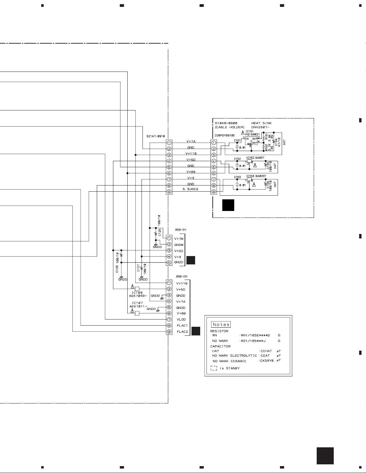
REGB ASSY
H
SEMICONDUCTORS
IC153 BA033T
IC152 BA05T
IC151 PQ15RW21
CAPACITORS
C155, C156 CEHAT101M10
C154 CEHAT470M16
C151–C153 CKSRYB103K50
RESISTORS
R152 RN1/16SE2201D
R151 RN1/16SE3901D
OTHERS
151 9P CABLE HOLDER 51048-0900
J 151 JUMPER WIRE D20PDY0910E
0 REGURATOR PLATE DNH2507
SCREW BBZ30P060FMC
RESISTORS
Other Resistors RS1/16S&&& J
OTHERS
CN106 9P JUMPER CONNECTOR 52147-0910
CN103 SOCKET 4P AKP7132
CN104 5P TOP POST B5B-EH
CN105 9P TOP POST B9B-EH
0 SCREW PLATE VNE1948
ACIN ASSY
G
SWITCHES AND RELAYS
S101 RSA1001
CAPACITORS
C102 (0.01µF/ AC275V ACE7027
C101 (10000PF/AC250V) ACG7033
OTHERS
CN102 PLUG 4P AKM7055
AN101 POWER SOCKET AKP7032
H101, H102 FUSE CLIP AKR1004
53
Page 54

CMX-3000, CU-V163
Mark No. Description Part No. Mark No. Description Part No.
CNTA ASSY
I
SEMICONDUCTORS
IC301 PD5764A
IC305 TC74HC14AF
IC303, IC304 TC7S86F
Q361–Q373, Q403, Q404 ,Q406 2SC4081
Q408–Q410 2SC4081
D301, D302, D396–D399 1SS355
D411, D412 SLI-343URCW(RST)
D415–D420 SLI-343YCW(RST)
D407–D410 TLGE68TG(NP)
SWITCHES
S301–S308, S311–S313 ASG7013
S341–S347 ASG7013
CAPACITORS
C451 CEAT101M10
C458 CEAT1R0M50
C459 CEAT220M50
C301, C311, C396–C399 CKSRYB102K50
C452–C455, C457 CKSRYB103K50
SWITCHES
CAPACITORS
RESISTORS
D623–D628, D631–D636 SLI-343YCW(RST)
D607–D610 TLGE68TG(NP)
D590 UDZS5.1B
S501–S508, S511–S515 ASG7013
S521–S526, S531–S536 ASG7013
S541–S547 ASG7013
C651 CEAT101M10
C658 CEAT1R0M50
C659 CEAT220M50
C501, C511, C521, C531, C541 CKSRYB102K50
C596–C599, C656 CKSRYB102K50
C652–C655, C657 CKSRYB103K50
C683–C700 CKSRYB221K50
R596, R597 RS1/16S2201F
VR501 (50kΩ-B x2) DCV1011
Other Resistors RS1/16S&&& J
C483–C500 CKSRYB221K50
C461, C462 CKSRYB471K50
RESISTORS
R396, R397 RS1/16S2201F
VR301 (50kΩ-B x2) DCV1011
Other Resistors RS1/16S&&& J
OTHERS
CN303 CONNECTOR 52084-1510
CN301 4P JUMPER CONNECTOR 52147-0410
V301 VACUUM FL DISPLAY DEL1047
X301 CERAMIC RESONATOR DSS1131
FL HOLDER DNK3956
PHTA ASSY
J
SEMICONDUCTORS
D391, D392 GP1S94
CAPACITORS
C391 CKSRYB103K50
RESISTORS
Other Resistors RS1/16S&&& J
OTHERS
J 302 JUMPER WIRE D20PWY0415E
CNTB ASSY
K
SEMICONDUCTORS
IC501 PD5764A
IC502 PST994D
IC503 TC74AC04F
Q561–Q573, Q601–Q604, Q606 2SC4081
Q608–Q618 2SC4081
D501, D596–D599 1SS355
D611, D612, D621, D 622 SLI-343URCW(RST)
D629, D 630 SLI-343URCW(RST)
D601–D604, D615–D620 SLI-343YCW(RST)
OTHERS
CN504 CONNECTOR 52084-0810
CN503 CONNECTOR 52084-0910
CN501 4P JUMPER CONNECTOR 52147-0410
V501 VACUUM FL DISPLAY DEL1047
X501 CERAMIC RESONATOR (4MHz) DSS1131
FL HOLDER DNK3956
PHTB ASSY
L
SEMICONDUCTORS
D591, D592 GP1S94
CAPACITORS
C591 CKSRYB103K50
RESISTORS
Other Resistors RS1/16S&&& J
OTHERS
J 502 JUMPER WIRE D20PWY0415E
CNNB ASSY
M
SEMICONDUCTORS
IC701 BA05T
CAPACITORS
C703 CEAT101M10
C701 CEAT101M16
C702, C704 CKSRYB103K50
OTHERS
CN704 CONNECTOR 8P 53095-0810
CN703 CONNECTOR 9P 53095-0910
CN702 CONNECTOR 15P 53095-1510
0 I/O JACK VKN1070
0 SCREW PLATE VNE1948
54
Page 55

6. ADJUSTMENT
6.1 ADJUSTMENT ITEMS AND LOCATION
Adjustment Points (PCB Part)
CMX-3000, CU-V163
MAIN ASSY
A
SIDE A
PLAYER A
IC1415
VCO-TP
PLAYER B
IC1414
VCO-TP
Adjustment Items
[Electrical Part]
1
VCO Free-running Adjustment
6.2 JIGS AND MEASURING
INSTRUMENTS
Screwdriver (small)
Dual-trace oscilloscope
(10:1 probe)
VC1001VC1001 VC1001VC1002
PLAYER A PLAYER B
6.3 NECESSARY ADJUSTMENT POINTS
CH1 CH2
(X) (Y)
Exchange
MAIN ASSY
Exchange
CD MECHANISM ASSY
(DA11T3CNPIO)
When Adjustment Points
1
= Page 56
55
Page 56

CMX-3000, CU-V163
6.4 ELECTRICAL ADJUSTMENT
1
VCO Free-running Adjustment
Objective : To optimize the VCO free-running frequency
When not properly adjusted :
• Master Tempo does not function normally
• The output does not appear in indication and occasion
when turned a Tempo adjustment into + side.
• Power ON
• None disc
START
Player
MAIN ASSY
IC1415 - pin 1 (PLAYER A)
IC1414 - pin 1 (PLAYER B)
GND
MAIN ASSY
VC1001 (PLAYER A)
VC1002 (PLAYER B)
Probe (10:1)
DC voltage
2.5±0.2V
CH1 CH2
(X) (Y)
Oscilloscope
V: 50mV/div.
H: 10msec/div.
DC mode
56
Page 57

CMX-3000, CU-V163
7. GENERAL INFORMATION
7.1 DIAGNOSIS
7.1.1 SERVICE MODE
Outline of the Service Mode
This unit prepares the test mode in the controller and player sections.
1 Confirmation mode of the controller button and display function
There are following two ways in the mode confirming the controller button and display function.
Mode 1: When connect the Controller section to the Player, and confirm it.
Mode 2: When connect the power supply to Controller section being simple, and confirm it.
Basic operation is the same with both modes, but FL does not light.
2 The mode which confirms the operation with the player being simple (Use the remote control unit.)
Connect the Remote control unit (RU-V101) to a DATA IN/OUT terminal of the Player and confirms the operation.
3 State confirmation mode with the system operation
Confirm the software version of each microcomputer and active state with the display.
Confirmation Mode of the Controller Button and Display Function
• Mode 1
Enter this mode when turns the power on while pressing the AUTO button of each player simultaneously.
Mode 1 can confirm the state of each other button with FL other than the operation of mode 2.
• Mode 2
Enter this mode when connects a screw terminal to GND and +8V from the external DC power supply to V+8B by
controller section being simple. Further, it is not necessary to press buttons in the power-up.
GND
+8V
V+8B
GNDD
GNDD
CNNB Assy
Fig.1 External DC Power Supply Connection Position
Note : Mode 1 and mode 2 are the same operations basically. But a power supply of FL system is not supplied in case of mode 2.
Therefore cannot confirm it with FL.
Explain the operation about mode 1 here. (Mode 2 is the same except that FL of mode 1 does not light.)
PLAYER A PLAYER B
G9
G10
FL Display Section
and the Grid Division.
V+8B
G1 G2 G3 G4 G5 G6 G7 G8
G12
G11
G13
37seg × 13grid
Fig. 2 Controller Button and FL Display Section
57
Page 58

CMX-3000, CU-V163
• Confirm the FL display operation
In mode 1, display the demonstration display of fixed pattern and display 1/2 light, all lighting and all lights out repeatedly.
In addition, display the button name in dot matrix of Grid 1 to Grid 8 while a button is pressed.
• Confirm the each button operation
Corresponding two LED lights when pressed the button of each player.
Relation of LED corresponding to each button is the following matrix, and vertical scale of each button and button LED
corresponding to horizontal scale light it.
For example, "CUE" button LED of player B and "HOT CUE 1" button LED of player A light it when pressed "EJECT" button of
player B.
When "BPM SYNC" and "RELAY PLAY" button were pressed, "CUE" button LED of player B and "HOT CUE (REC)" button
LED of player A and "HOT CUE 3" button LED of player B light it.
PLAY/PAUSE (6)
Button LED
of Each Player
HOT CUE 3_a Button LED SERCH (1) MASTER TEMPO HOT CUE 1 PLAY/PAUSE (6)
HOT CUE 2_a Button LED SERCH (¡) TEMPO RANGE HOT CUE 2 CUE
HOT CUE 1_a Button LED TRACK SERCH (4) EJECT HOT CUE 3 IN/REALTIME CUE
HOT CUE (REC)_a Button LED TRACK SERCH (¢) BPM SYNC (Player B) HOT CUE (REC) OUT/OUT ADJ
HOT CUE 3_b Button LED TIME MODE / AUTO CUE RELAY PLAY (Player B) AUTO JOG MODE
HOT CUE 2_b Button LED CD TEXT / WAVE TAP EXIT/RELOOP
HOT CUE 1_b Button LED PITCH BEND (+) EMERGENCY LOOP
HOT CUE (REC)_b Button LED PITCH BEND (−)
CUE Button LED
of Each Player
IN/REALTIME CUE
Button LED
of Each Player
OUT/OUT ADJ Button
LED
of Each Player
In the mode 1, display the button name to correspond in dot matrix in the FL.
Button FL Display Button FL Display
SEARCH (1) Button SERCH 1 HOT CUE 1 Button HOTCUE 1
SEARCH (¡) Button SERCH ¡ HOT CUE 2 Button HOTCUE 2
TRACK SEARCH (4) Button TRACK 4 HOT CUE 3 Button HOTCUE 3
TRACK SEARCH (¢) Button TRACK ¢ HOT CUE (REC) Button HOT REC
TIME MODE / AUTO CUE Button TIME/CUE AUTO Button AUTO
CD TEXT / WAVE Button TEXTWAVE TAP Button TAP
PITCH BEND (+) Button PITCH + PLAY/PAUSE (6) Button PLAY
PITCH BEND (−) Button PITCH − CUE Button CUE
MASTER TEMPO Button M.T ∗∗∗ (Note ∗1) IN/REALTIME CUE Button LOOP IN
TEMPO RANGE Button TEMPO ∗∗∗ (Note ∗1) OUT/OUT ADJ Button LOOP OUT
EJECT (0) Button EJECT JOG MODE Button JOG MODE
BPM SYNC Button BPM SYNC ∗2 EXIT/RELOOP Button RELOOP
RELAY PLAY Button RELAY PL ∗2 EMERGENCY LOOP Button EM. LOOP
Note ∗1 : Reading value of the TEMPO slider (+10 to 0 to −10) displays in ∗ ∗ ∗.
∗2 : Display in FL of the player B side.
• Confirm the JOG operation
Button LED corresponding to each JOG blinks when turned JOG.
When JOG of player A side moves: RELAY PLAY button LED light or turn off the light in the state of the JOG address that read in.
When JOG of player B side moves: BPM SYNC button LED light or turn off the light in the state of the JOG address that read in.
• Confirm the each button LED
In this unit, all button LED light fixed time at the power-up.
In addition, it can confirm the lighting state by performing the "Confirm the each button operation", "Confirm the JOG operation"
and "Confirm the TEMPO slider".
58
Page 59

CMX-3000, CU-V163
• Confirm the TEMPO slider
In the position which read-in from the TEMPO slider, MT button LED lights at + side, and MT button LED turns off the light at
− side.
However, there is a case that lights or turns off the light for unevenness of parts of TEMPO slider at the center tap periphery.
In addition, when TEMPO button and MT button were pressed in mode 1, match with button name in dot matrix in the FL, and
display reading value of TEMPO slider by a value of +10 to 0 to −10.
Confirmation Mode of Operation with the Player Being Simple
Connect the remote control unit (RU-V101) to DATA IN/OUT terminal of the Rear panel of the player section, and confirm the
operation.
When use the remote control unit, remove a connection cable with the control section before power-up, then connect the remote
control unit.
DATA
IN/OUT
REJECT PAUSE
AUDIO SPEED OPEN
DISPLAY STILL C-MODE
FRAME TIME CHAPTER
PLAY
STILL/STEP
– MULTI-SPEED +
SCAN
SEARCH
FUNCCLEAR
CR
789
456
VIDEO STOP.M START
123
0
ABC
Remote control unit
for service
(RU-V101)
Fig. 3 Connection of the Remote Control Unit for Service
• Function of the remote control unit (RU-V101) for service
REJECT PAUSE
789
AUDIO SPEED OPEN
456
VIDEO STOP.M START
123
DISPLAY STILL C-MODE
0
FRAME TIME CHAPTER
ABC
PLAY
STILL/STEP
– MULTI-SPEED +
SCAN
FUNCCLEAR
SEARCH
CR
Player Select
A Time Mode Set
Track Mode Set
Frame Mode Set
Play
(Reject)
(Pause)
(Search)
(Scan Forward)
(Scan Reverse)
(1 Track Search Forward)
(1 Track Search Reverse)
(Eject)
(Speed)
(X Speed)
(Test / Normal Mode Change)
(Servo All OFF)
(Focus ON)
(Spindle Kick, Tracking ON / OFF)
(Tracking OFF)
(Slide FWD)
(Slide REV)
(Search TR No. 2)
[ Rear view ]
Button Corresponding
to RU-V101
STOP. M (FUNC + 5)
TIME
CHAPTER
FRAME
PLAY 3
REJECT 0
PAUSE 8
SEARCH
SCAN ¡
SCAN 1
STILL / STEP E
STILL / STEP e
OPEN (FUNC + 9)
SPEED (FUNC + 8)
A (FUNC + FRAME)
C-MODE (FUNC + 3)
0 + TIME
1 + TIME
2 + TIME
3 + TIME
4 + TIME
5 + TIME
6 + TIME
Digital SW OFF
in CDJ Mode
?
?
?
?
Track Search
?
?
?
Digital SW ON
in Digital Mode
?
?
?
?
?
?
?
?
?
?
?
?
?
?
?
?
?
?
?
?
?
?
?
• Specification method of the player issuing the command
One remote control unit is prepared for two players in this unit.
It is necessary to specify the player beforehand when issues the command to each player.
Specification method of player A (left side from the front): Press buttons of "1", "STOP.M" ("FUNC" and "5") in order.
Specification method of player B (right side from the front): Press buttons of "2", "STOP.M" ("FUNC" and "5") in order.
Command is published by the specified player till the next Player Select command is issued after this command issue.
59
Page 60

CMX-3000, CU-V163
• Specification method of addressing modes in the search
There are three ways of search methods of time search, track search and frame search in this unit.
It is necessary to specify each mode when performs each search.
• Time search (A Time mode set)
Set absolute time (minute, second, frame) in the address mode.
[Examples] When search for 2 minutes 34 seconds 56 frame:
• Track search (Track mode set)
Set track number in the address mode.
[Examples] When search for track 5:
• Frame search (Frame mode set)
Set frame in the address mode.
[Examples] When search for 1200 frame:
• Player operation command
(Play) : Playback
(Reject) : Stop
Press buttons of "TIME", "0", "2", "3", "4", "5", "6" and "SEARCH" in order.
Press buttons of "CHAPTER", "5" and "SEARCH" in order.
Press buttons of "1", "2", "0", "0" and "SEARCH" in order.
(Pause) : Pause. Also stop the scan operation during scan, and become pause.
(Scan Forward) : Perform the scan opearation in the forward direction.
(Scan Reverse) : Perform the scan opearation in the reverse direction.
(1 Track Search Forward) : Perform the track search in the forward direction.
(1 Track Search Reverse) : Perform the track search in the reverse direction.
(Eject) : Perform the disc eject either Playback state or Stop state.
(Speed) : In the CDJ mode, set the playback speed (tempo) that specified with the argument.
Become the sound output pause in the CDJ mode.
Press the PAUSE button when completes the scan operation.
Press the PAUSE button when completes the scan operation.
An argument is three columns of figure and specify 0: − (minus) or 1: + (plus) with 100-place.
And specify (from 0 to 16) a tempo (%) by two places of remainders.
Example: It becomes the +1% setting by pressing buttons of "1", "0", "1", "SPEED" ("FUNC" and "8") in order.
It becomes the −10% setting by pressing buttons of "0", "1", "0", "SPEED" ("FUNC" and "8") in order.
It becomes the +16% setting by pressing buttons of "1", "1", "6", "SPEED" ("FUNC" and "8") in order.
60
Page 61

CMX-3000, CU-V163
• Test operation command
As for the following command, an operation becomes possible in the digital mode (digital mode switch of front panel is ON).
Because there is a case to damage the player when test operation command mistakes usage, be careful.
(X Speed) : In the digital mode, switch the rotation speed of the player to normal speed and double speed .
Further, sound cannot output in the double speed.
Example:
It becomes the normal speed playback setting by pressing buttons of "1" and "A" ("FUNC" and "FRAME") in order.
It becomes the double speed playback setting by pressing buttons of "2" and "A" ("FUNC" and "FRAME") in order.
∗ This command issues a command by stopped state in order to issue a command to servo DSP directly.
(Test/Normal Mode Change) : Switch the Test mode/Normal mode by "C-MODE" ("FUNC" and "3") buttons.
Can use only commands of 6TM from 0TM in the test mode.
(Servo All OFF) : During servo ON, turn all servo OFF when pressing "0" and "TIME" buttons in order.
(Focus ON) : During CD STOP, turn the LD ON and perform the auto focus when pressing "1" and "TIME" buttons in order.
(Spindle Kick and Tracking ON/OFF) : During tracking servo OFF, perform the spindle kick and turn the automatic adjustment
processing and tracking servo ON when pressing "2" and "TIME" buttons in order.
Also during tracking servo ON, turn the tracking servo OFF when pressing "2" and "TIME"
buttons in order.
(Tracking OFF) : During tracking servo ON, turn the tracking servo OFF when pressing "3" and "TIME" buttons in order.
(Slide FWD) : During tracking servo ON, Turn the tracking servo OFF and move the slider in the FWD direction when pressing "4"
and "TIME" buttons in order.
(Slide REV) : Turn the tracking servo OFF and move the slider in the REV direction when pressing "5" and "TIME" buttons in order
during tracking servo ON.
(SEARCH TR No. 2) : During CD STOP, perform the following operation when pressing "6" and "TIME" buttons in order.
LD ON - Auto focus - Spindle kick - automatic adjustment processing - Second tune search - Tracking
servo ON
When performed Tracking OFF, there is the case that cannot rise up in this command.
In that case please repeat once again after power OFF and ON.
∗ : When rise up by a step with the test mode, input a command by pressing buttons of "0", "TIME", "1", "TIME", "2" and "TIME" in
order.
State Confimation Mode in the System Operation
The mode which confirms confirmation and operating state of software version of each microcomputer by display.
• Confirmation method of the microcomputer software version of the controller section
Load two microcomputers on the controller section.
As for the symptom of a version of each microcomputer, dot matrix is displayed for about 2 seconds while pressing each PITCH
BEND (+) button by turning the power on.
• Confirmation method of the player section
Player section processes both players with one microcomputer.
As for the method to confirm a microcomputer version, a version is displayed by long push of CD TEXT/WAVE button and
OUT/OUT ADJ button in FL.
61
Page 62

CMX-3000, CU-V163
7.1.2 STARTING SEQUENCE
Disc loding completion
Foucus and Tracking Offset Adjustments
Spindle preliminary kick
LD ON
Foucus sweep and Focus ON It fails 3 times and becomes CD-RW mode
RF-amp gain up and it becomes a Foucus sweep It Error-displays by 3 times
FOK Check
Spindle acceleration 100 msec
CLV Servo ON
It waits and is 300msec
Tracking Close
GFS Check
Tracking Balance Adjustment (T Open)
Focus Balance Adjustment TOC• TEXT (if it is)
Data lead
Focus Gain Adjustment
(E-8301)
Tracking Gain Adjustment
RF Gain Adjustment
Search for Track No.1
(A Slider is moved to an inside circumference)
Line Speed measuremnt
Search for Track No.1
2 Track Jump Back
Waiting for a target address
Play (mute off)
62
Page 63

CMX-3000, CU-V163
7.1.3 DISASSEMBLY
(1) CMX-3000
Bonnet
Bonnet
1
1
1
MAIN Assy - Player Section
Remove the Bonnet.
1
Rear View
2
Front panel Section
Remove the Bonnet.
1
Front Panel
2
x
8
1
1
12
3
1
1
Remove the connector.
x
9
15
JACB Assy
Cord Clamper
3
x
7
3
x
5
14
Panel Stay
MAIN Assy
Cord Clamper
16
3
3
63
Page 64

CMX-3000, CU-V163
SLOT-IN MECHANISM Assy SERVO MECHANISM Assy
1
2
A
PLAYER
×2
×2
1
1
2
B
PLAYER
B
PLAYER
Bottom PalateBottom Palate
Bottom PalateBottom Palate
A
PLAYER
A
PLAYER
2
1
×2
B
PLAYER
1
×2
1
5
2
Short land
3
4
Float Spring R
Float Spring R
(Silver)
(Silver)
5
7
3
6
Float Spring F
Float Spring F
(Black)
Note:
Servo Mechanism Assy can diagnose and remove it from the
backside.
(Inverts the product, and not performing the operation check.)
[Caution in the Servo Mechanism Assy replacement]
• When remove the Servo Mechanism Assy, short-circuit a LD Short land 5 before disconnecting a flexible cable
from the connector.
When install the Servo Mechanism Assy, release the short-circuit of LD Short land 5 after connecting the flexible
cable to the connector. (For LD fracture prevention)
4
Servo Mechanism AssyServo Mechanism Assy
(Black)
4
4
• Installing the Froat Spring F and Froat Spring R to the correct position.
Front side : Froat Spring F (Black) x2
Rear side : Froat Spring R (Silver) x2
64
Page 65

The Operation check method of a mechanism unit
Remove the Bonnet
1
CMX-3000, CU-V163
Cord clamper is loosened.
x4
4
3
3
x2x3
2
2
2
2
2
3
x2x3
3
x2x2
2
5
Unit part is shifted on a rear side.
Unit part.
Slit
Hook
6
The Hook of a rear panel is put in to a slit.
Rear Panel
7
Diagnosis of
8
a mechanism unit.
65
Page 66

CMX-3000, CU-V163
(2) REMOTE CONTROLLER (CU-V163)
Rear Panel
1
×9
12
Rear PanelRear Panel
CNTA, CNTB Assy
1
Note :
When cuts PC Board with a nipper and replaced slide VR,
positioning becomes invalid. Please aline it by visual inspection
when installs it. (Refer to the following diagram.)
×3
×3
3
CNTB Assy
CNNB AssyCNNB Assy
3
1
2
2
CNNB AssyCNTA Assy
Cut Point
(x 6)
This illustration is CNTB Assy.
JOG Dial
Remove the CNTA, CNTB and CNNB Assy
1
×4
×6
3
×3
×3
×4×4
3
2
×5×2
2
×5×2
2
×5×2
2
×5×2
CNTB Assy
11 1312
CNTA Assy
1 11142
66
,,
4
,,
×16
×3×3
×10
[ Rear view ]
×3×3
4
3
×5×4
Unhook
×3×4
4
Remove the Front Panel Assy
4
Page 67

JOG Dial Section
1
CMX-3000, CU-V163
1
1
1
CNNB AssyRetainer
Display Plate
CNNB Assy
CNNB AssyJOG Ring
CNNB AssyJOG Dial
Grease
Grease
(GYA1014)
(GYA1014)
A hand driver fastens a screw.
The screw tightening torqueThe screw tightening torque
The screw tightening torque
0.098 ± 0.01% [N • m]
0.098 ± 0.01% [N
Steel Ball
Grease is applied to three
places every two pieces.
×9
• m]
×4
Front side
Hook
(x 10)
Magnet Stay
Magnet
Super X
(GYL1004)
67
Page 68

CMX-3000, CU-V163
7.2 PARTS
7.2.1 IC
• The information shown in the list is basic information and may not correspond exactly to that shown in the schematic diagrams.
List of IC
•
NJM2870F18, NJM2870F25, NJM2360M, PST994D, TC74VHC04FT, XC2S30-5TQ144C, TA2153FN, PD5764A,
HD6417709AF100B
NJM2870F18 (MAIN ASSY : IC1406)
• Regulator IC
Pin Arrangement
15
2
34
PIN FUNCTION
1. CONTROL (Active High)
2. GND
3. NOISE BYPASS
OUT
IN
4. V
5. V
Block Diagram
VIN
Cont
Bandgap
Reference
GND
NJM2870F25 (MAIN ASSY : IC1009)
• Regulator IC
Pin Arrangement
15
2
34
PIN FUNCTION
1. CONTROL (Active High)
2. GND
3. NOISE BYPASS
OUT
IN
4. V
5. V
Thermal
Protection
V
OUT
Noise
Bypass
Block Diagram
68
VIN
Cont
GND
Bandgap
Reference
Thermal
Protection
V
OUT
Noise
Bypass
Page 69

NJM2360M (JACB ASSY : IC211)
• DC-DC Convertor
Pin Arrangement
Block Diagram
CMX-3000, CU-V163
PST994D (CNTB ASSY : IC502)
• Reset IC
Block Diagram
TC74VHC04FT (MAIN ASSY : IC1437)
• Logic IC
Pin Arrangement
69
Page 70

CMX-3000, CU-V163
XC2S30-5TQ144C (MAIN ASSY : IC1409)
• PLD IC
Pin Name
Pin No. Pin No. Pin No.Port Name
1 Vcco Vcco 51 D6 I/O,IRDY 101 I/O
2 TCK TCK 52 GND GND 102 XCS5 I/O,Vref
3 EX_CONT2_A I/O 53 VCCO VCCO 103 XCS2 I/O
4 DAC1_MCLK I/O 54 D7 I/O,Trdy 104 STATUS STATUS
5 DAC1_BCK I/O,Vref 55 Vccint Vccint 105 PWDN PWDN
6 DAC1_LRCK I/O 56 A1 I/O 106 M2 M2
7 DAC1_DATA I/O 57 A2 I/O(D4) 107 VCCO Vcco
8 GND GND 58 MREQB I/O,Vref 108 VCCO Vcco
9 Vccint Vccint 59 XRD I/O 109 M0 M0
10 DAC2_MCLK I/O 60 XWE I/O(D5) 110 GND GND
11 DAC2_BCK I/O 61 GND GND 111 M1 M1
12 DAC2_LRCK I/O,Vref 62 MREQA I/O(D6) 112 A25 I/O
13 DAC2_DATA I/O 63 BCLKA I/O 113 A24 I/O
14 Vccint Vccint 64 I/O 114 A23 I/O
15 CKIO GCK3 65 DSP1BCK I/O,Vref 115 A3 I/O,Vref
16 VCCO Vcco 66 DBCLKA I/O 116 I/O
17 GND GND 67 DSP1LRCK I/O(D7) 117 D8 I/O
18 PLLCLK GCK2 68 INIT I/O(INIT) 118 D9 I/O
19 GND I/O 69 XPROGRAM PROGRAM 119 GND GND
20 EX_CONT1B I/O 70 Vcco Vcco 120 D10 I/O
21 EX_CONT2B I/O,Vref 71 Vcco Vcco 121 D11 I/O
22 SBOK2 I/O 72 DONE DONE 122 D12 I/O,Vref
23 SUBQ2 I/O 73 GND GND 123 D13 I/O
24 Vccint Vccint 74 SDI0A I/O 124 D14 I/O
25 GND GND 75 SDI1A I/O 125 Vccint Vccint
26 SBSY2 I/O 76 SDI2A I/O 126 D15 I/O,TRDY
27 I/O 77 SDI2B I/O,Vref 127 Vcco Vcco
28 SFSY2 I/O,Vref 78 DSP2DATA I/O 128 GNDGND
29 LRCK2 I/O 79 DSP1DATA I/O 129 RD/XWR I/O,IRDY
30 BCK2 I/O(WRITE) 80 SDI1B I/O 130 XDREQ1 I/O
31 ADATA2 I/O(CS) 81 GND GND 131 XDREQ0 I/O
32 TDI TDI 82 Vccint Vccint 132 SUBQ1 I/O,Vref
33 GND GND 83 DISC_LED_A I/O 133 SBSY1 I/O
34 TDO TDO 84 DISC_LED_B I/O 134 I/O
35 Vcco Vcco 85 G2 I/O,Vref 135 GND GND
36 Vcco Vcco 86 A2 I/O 136 SBOK1 I/O
37 CCLK CCLK 87 GND I/O 137 SFSY1 I/O
38 I/O(DOUT,BUSY) 88 ACLK2 GCK0 138 ADATA1 I/O
39 DIN I/O(DIN,D0) 89 GND GND 139 LRCK1 I/O,Vref
40 BCLKB I/O 90 Vcco Vcco 140 BCK1 I/O
41 DBCLKB I/O,Vref 91 ACLK1 GCK1 141 EX_CONT1_A I/O
42 I/O 92 Vccint Vccint 142 TMS TMS
43 SDI0B I/O 93 G1 I/O 143 GND GND
44 D0 I/O(D1) 94 A1 I/O,Vref 144 VCCO VCCO
45 GND GND 95 I/O
46 D1 I/O(D2) 96 XDACK1 I/O
47 D2 I/O 97 Vccint Vccint
48 D3 I/O,Vref 98 GND GND
49 D4 I/O(D3) 99 XDACK0 I/O
50 D5 I/O 100 XRST I/O
Pin Name
Port Name
Pin Name
Port Name
NC
NC
Pin Name
70
Page 71

Pin Function (1/2)
PLL
Pin No.
Pin Name Description
18
PLLCK I
91
ACLK1 VCO input for CD1
G1 O Phase comparison machine output for CD1
93
94
A1 O Phase comparison machine output for CD1
88
ACLK2 VCO iinput for CD2
85
G2 O PLL output for CD2
A2 O PLL output for CD2
86
DSP I/F
Pin Name Description
Pin No.
MREQA I Ach REQ signal CD1
62
63
BCLKA O Bit clock output terminal, clock for audio data
66
DBCLKA O Word clock output terminal
74
SDI0A O Serial audio data output terminal 0
75
SDI1A O Serial audio data output terminal 1
DSI2A O Data lead
76
58
MREQB I
40
BCLKB O bit clock output terminal, clock for audio data
41
DBCLKB O Word clock output terminal
SDI0B O Serial audio data output terminal 0
43
80
SDI1B O Serial audio data output terminal 1
77
DSI2B O Data lead
I/O
16. 9344MHz Standard Frequency Input
I
I
I/O
Bch REQ signal CD2
CMX-3000, CU-V163
Connection Point
Standard Frequency area
VCO area
VCO area
VCO area
VCO area
VCO area
VCO area
Connection Point
DSP Ach
DSP Ach
DSP Ach
DSP Ach
DSP Ach
DSP Ach
DSP Ach
DSP Ach
DSP Ach
DSP Ach
DSP Ach
DSP Ach
AUDIO INPUT I/F
Pin No.
Pin Name I/O Description
140 BCK1 bit clock for audio input from CD1 D Servo IC1
139 LRCK1 LR clock for audio input from CD1 D Servo IC1
138 ADATA1 audio data from CD1 D Servo IC1
133 S BSY1 sub code sync. from CD1 D Servo IC1
137 S FSY1 frame sync. from CD1 D Servo IC1
132 S UBQ1 sub code Q data from CD1 D Servo IC1
136 S BOK1 sub code Q data CRCC judging result input terminal from CD1 D Servo IC1
30 BCK2 bit clock for audio input from CD2 D Servo IC2
29 LRCK2 R clock for audio input from CD2 D Servo IC2
31 ADATA2 audio data from CD2 D Servo IC2
26 S BSY2 sub code sync. from CD2 D Servo IC2
28 S FSY2 frame sync. from CD2 D Servo IC2
23 S UBQ2 sub code Q data from CD2 D Servo IC2
22 S BOK2 sub code Q data CRCC judging result input terminal from CD2 D Servo IC2
AUDIO DATA CHANGE
Pin No.
Pin Name Description
65 DSP1BCK
DSP1LRCK
67
DSP1DATA
79
78
DSP2DATA
DAC I/F
Pin No.
Pin Name Description
4 DAC1_MCLK O
5 DAC1_BCK O bit clock for DAC1
6 DAC1_LRCK O LR clock for DAC1
7 DAC1_DATA O data for DAC1
10 DAC2_MCLK O data for DAC2
11 DAC2_BCK O bit clock for DAC2
12 DAC2_LRCK O LR clock for DAC2
13 DAC2_DATA O data for DAC2
I
I
I
I
I
I
I
I
I
I
I
I
I
I
I/O
I audio data is changed DSP
audio data is changed
I
audio data is changed
I
I
audio data is changed
I/O
clock for DAC1
Connection Point
Connection Point
DSP
DSP
DSP
Connection Point
DAC1
DAC1
DAC1
DAC1
DAC2
DAC2
DAC2
DAC2
71
Page 72

CMX-3000, CU-V163
Pin Function (2/2)
CPU I/F
Pin No.
102
103
112
113
114
115
57
56
126
124
123
122
121
120
118
117
54
51
50
49
48
47
46
44
130
131
96
99
60
59
129
15
100
Pin Name Description
XCS5 I CH input for address decoding
XCS2 I CH input for address decoding
A25 I CH input for address decoding
A24 I CH input for address decoding
A23 I
A3 address input terminal for CPU
A2
A1
D15 I/O
D14 I/O
D13 I/O
D12 I/O
D11 I/O
D10 I/O
D9 I/O
D8 I/O
D7 I/O
D6 I/O
D5 I/O
D4 I/O
D3 I/O
D2 I/O
D1 I/O
D0 I/O
XDREQ1 O data request
XDREQ0 O
XDACK1 I
XDACK0 I
XWE I write enable signal
XRD I read strobe signal
RD/XWR I
CKIO system clock
XRST system reset
I/O
CH input for address decoding
I
I
address input terminal for CPU
I
address input terminal for CPU
address input terminal for CPU
address input terminal for CPU
address input terminal for CPU
address input terminal for CPU
address input terminal for CPU
address input terminal for CPU
address input terminal for CPU
address input terminal for CPU
address input terminal for CPU
address input terminal for CPU
address input terminal for CPU
address input terminal for CPU
address input terminal for CPU
address input terminal for CPU
address input terminal for CPU
address input terminal for CPU
data request
data akunoridge
data akunoridge
read write signal
I
I
Connection Point
SH3
SH3
SH3
SH3
SH3
SH3
SH3
SH3
SH3
SH3
SH3
SH3
SH3
SH3
SH3
SH3
SH3
SH3
SH3
SH3
SH3
SH3
SH3
SH3
SH3
SH3
SH3
SH3
SH3
SH3
SH3
SH3
SH3
CPU I/O EXTENSION
Pin No.
CONFIGURATION OTHERS
Pin No.
Pin Name
141 EX_CONT1_A I/O
3 EX_CONT2_A
20 EX_CONT1B
21 EX_CONT2B I
83 DISC_LED_A O
84 DISC_LED_B O
Pin Name
109 M0 I
111 M1 I
106 M2 I
69 XPROGRAM O
39 DIN
68 XINIT O
37 CCLK I/O
72 DONE O
I/O
I/O
I/O
Description
I
Description Description
9, 14, 24, 55
82, 92, 97, 125
1, 35, 36, 53, 70
71, 90, 107, 108
I
127,144
8, 17, 19, 25, 33
45, 52, 61, 73, 81
87, 98, 110, 135
143
72
Pin No.
Pin Name
Vccint 2.5V
Vccco
GND GND
I/O
3.3V
Connection Point
Page 73

TA2153FN (MAIN ASSY : IC1003, IC1010)
• RF Amp IC
Block Diagram
CMX-3000, CU-V163
73
Page 74

CMX-3000, CU-V163
Pin Function (1/2)
74
Page 75

Pin Function (2/2)
CMX-3000, CU-V163
75
Page 76

CMX-3000, CU-V163
PD5764A (CNTB ASSY : IC501)
• Micro computer (Master CPU)
Pin Function
76
Pin
Pin Name
No
1
KEY5 I Key Input
2
KEY4 I Key Input
3
KEY3 I Key Input
4
KEY2 I Key Input
5
KEY1 I Key Input
6
KEY0 I Key Input
7
LED7 O BPM SYNC 1: Light up
8
LED6 O RELAY PLAY 1: Light up
9
NC O -
10
LED4 O PLAY/ PAUSE 1: Light up
11
LED3 O CUE 1: Light up
12
LED2 O IN/ REALTIME CUE 1: Light up
13
LED1 O OUT/ OUT ADJAST 1: Light up
14
LED0 O MT 1: Light up
15
NC O -
16
NC O -
17
CNVss -
18
XRESET I
19
NC O -
20
NC O -
21
GND - GND
22
XIN I 4MHz
23
XOUT O 4MHz
24
Vcc - +5V
25
LED15 O HOT REC : A 1: Light up
26
LED14 O HOT CUE1 : A 1: Light up
27
LED13 O HOT CUE2 : A 1: Light up
28
LED12 O HOT CUE3 : A 1: Light up
29
LED11 O HOT REC : B 1: Light up
30
LED10 O HOT CUE1 : B 1: Light up
31
LED9 O HOT CUE2 : B 1: Light up
32
LED8 O HOT CUE3 : B 1: Light up
33
XUNIT I -
34
XSTEP I -
35
TxD O Communication with a main part.
36
RxD I Communication with a main part.
37
S36 O FL Disply Segment 1: Light up
38
S35 O FL Disply Segment 1: Light up
39
S34 O FL Disply Segment 1: Light up
40
S33 O FL Disply Segment 1: Light up
41
S32 O FL Disply Segment 1: Light up
42
S31 O FL Disply Segment 1: Light up
43
S30 O FL Disply Segment 1: Light up
44
S29 O FL Disply Segment 1: Light up
45
S28 O FL Disply Segment 1: Light up
46
S27 O FL Disply Segment 1: Light up
47
S26 O FL Disply Segment 1: Light up
48
S25 O FL Disply Segment 1: Light up
49
S24 O FL Disply Segment 1: Light up
50
S23 O FL Disply Segment 1: Light up
I/O Discription
Pin
No
51
52
53
54
55
56
57
58
59
60
61
62
63
64
65
66
67
68
69
70
71
72
73
74
75
76
77
78
79
80
81
82
83
84
85
86
87
88
89
90
91
92
93
94
95
96
97
98
99
100
Pin Name
S22 O FL Disply Segment 1: Light up
S21 O FL Disply Segment 1: Light up
S20 O FL Disply Segment 1: Light up
S19 O FL Disply Segment 1: Light up
S18 O FL Disply Segment 1: Light up
S17 O FL Disply Segment 1: Light up
S16 O FL Disply Segment 1: Light up
S15 O FL Disply Segment 1: Light up
S14 O FL Disply Segment 1: Light up
S13 O FL Disply Segment 1: Light up
S12 O FL Disply Segment 1: Light up
S11 O FL Disply Segment 1: Light up
S10 O FL Disply Segment 1: Light up
S9 O FL Disply Segment 1: Light up
S8 O FL Disply Segment 1: Light up
S7 O FL Disply Segment 1: Light up
S6 O FL Disply Segment 1: Light up
S5 O FL Disply Segment 1: Light up
S4 O FL Disply Segment 1: Light up
S3 O FL Disply Segment 1: Light up
S2 O FL Disply Segment 1: Light up
S1 O FL Disply Segment 1: Light up
NC O NC O NC O G9 O FL Disply Grid 1: Light up
G1 O FL Disply Grid 1: Light up
G12 O FL Disply Grid 1: Light up
G13 O FL Disply Grid 1: Light up
G8 O FL Disply Grid 1: Light up
G10 O FL Disply Grid 1: Light up
G11 O FL Disply Grid 1: Light up
G2 O FL Disply Grid 1: Light up
G3 O FL Disply Grid 1: Light up
G4 O FL Disply Grid 1: Light up
G5 O FL Disply Grid 1: Light up
G6 O FL Disply Grid 1: Light up
G7 O FL Disply Grid 1: Light up
VLOAD - VLOAD
SINE1 I Automatic transmission Input.
SOUT1 O Automatic transmission Output.
SCLK11 I Automatic transmission Clock.
TYPE M/XS I High: Master CPU Mode.
SBUSY1 I Automatic transmission control line
XSRDY1 O Automatic transmission control line.
XRESET_S O Slave CPU Reset output 0: Reset
AGND - GND
AVREF - +5V
TEMPO_REF I TEMPO Slider Input.
TEMPO I TEMPO Slider Input.
I/O
Discription
Page 77

PD5764A (CNTA ASSY : IC301)
• Micro computer (Slave CPU)
Pin Function
Pin
No
Pin Name
1
NC O -
2
NC O -
3
NC O -
4
NC O -
5
KEY1 I -
6
KEY0 I -
7
NC O -
8
NC O -
9
NC O -
10
LED4 O PLAY/ PAUSE 1: Light up
11
LED3 O CUE 1: Light up
12
LED2 O IN/ REALTIME CUE 1: Light up
13
LED1 O OUT/ OUT ADJAST 1: Light up
14
LED0 O MT 1: Light up
15
JOG1A I A PLAYER JOG Input
16
JOG1B I B PLAYER JOG Input
17
CNVss - -
18
XRESET I -
19
JOG0A I A PLAYER JOG Input
20
JOG0B I B PLAYER JOG Input
21
GND - -
22
XIN I 4MHz
23
XOUT O 4MHz
24
Vcc - +5V
25
NC O -
26
NC O -
27
NC O -
28
NC O -
29
INT3 I B PLAYER JOG Trailing edge.
30
INT2 I B PLAYER JOG leading edge.
31
INT1 I A PLAYER JOG Trailing edge.
32
INT0 I A PLAYER JOG leading edge.
33
NC I -
34
NC I -
35
NC O -
36
NC I -
37
S36 O FL Disply Segment 1: Light up
38
S35 O FL Disply Segment 1: Light up
39
S34 O FL Disply Segment 1: Light up
40
S33 O FL Disply Segment 1: Light up
41
S32 O FL Disply Segment 1: Light up
42
S31 O FL Disply Segment 1: Light up
43
S30 O FL Disply Segment 1: Light up
44
S29 O FL Disply Segment 1: Light up
45
S28 O FL Disply Segment 1: Light up
46
S27 O FL Disply Segment 1: Light up
47
S26 O FL Disply Segment 1: Light up
48
S25 O FL Disply Segment 1: Light up
49
S24 O FL Disply Segment 1: Light up
50
S23 O FL Disply Segment 1: Light up
I/O
Discription
CMX-3000, CU-V163
Pin
No
51
52
53
54
55
56
57
58
59
60
61
62
63
64
65
66
67
68
69
70
71
72
73
74
75
76
77
78
79
80
81
82
83
84
85
86
87
88
89
90
91
92
93
94
95
96
97
98
99
100
Pin Name
S22 O FL Disply Segment 1: Light up
S21 O FL Disply Segment 1: Light up
S20 O FL Disply Segment 1: Light up
S19 O FL Disply Segment 1: Light up
S18 O FL Disply Segment 1: Light up
S17 O FL Disply Segment 1: Light up
S16 O FL Disply Segment 1: Light up
S15 O FL Disply Segment 1: Light up
S14 O FL Disply Segment 1: Light up
S13 O FL Disply Segment 1: Light up
S12 O FL Disply Segment 1: Light up
S11 O FL Disply Segment 1: Light up
S10 O FL Disply Segment 1: Light up
S9 O FL Disply Segment 1: Light up
S8 O FL Disply Segment 1: Light up
S7 O FL Disply Segment 1: Light up
S6 O FL Disply Segment 1: Light up
S5 O FL Disply Segment 1: Light up
S4 O FL Disply Segment 1: Light up
S3 O FL Disply Segment 1: Light up
S2 O FL Disply Segment 1: Light up
S1 O FL Disply Segment 1: Light up
NC O NC O NC O G9 O FL Disply Grid 1: Light up
G1 O FL Disply Grid 1: Light up
G12 O FL Disply Grid 1: Light up
G13 O FL Disply Grid 1: Light up
G8 O FL Disply Grid 1: Light up
G10 O FL Disply Grid 1: Light up
G11 O FL Disply Grid 1: Light up
G2 O FL Disply Grid 1: Light up
G3 O FL Disply Grid 1: Light up
G4 O FL Disply Grid 1: Light up
G5 O FL Disply Grid 1: Light up
G6 O FL Disply Grid 1: Light up
G7 O FL Disply Grid 1: Light up
VLOAD - VLOAD
SINE1 I Automatic transmission Input.
SOUT1 O Automatic transmission Output.
SCLK11 O Automatic transmission Clock.
TYPE M/XS I High: Master CPU Mode
SBUSY1 O Automatic transmission control line.
XSRDY1 I Automatic transmission control line.
NC O AGND - GND
AVREF - +5V
TEMPO_REF I TEMPO Slider Input.
TEMPO I TEMPO Slider Input.
I/O
Discription
77
Page 78

CMX-3000, CU-V163
HD6417709AF100B (MAIN ASSY : IC1204)
• Micro computer
Pin Function (1/4)
Pin
No.
1 MD1 MD1 I Pull up Clock mode setting
2 MD2 MD2 I Pull down Clock mode setting
3 Vcc-RTC Vcc-RTC
4 XTAL2 XTAL2 O NC Crystal resonator for internal RTC
5 EXTAL2 EXTAL2 I Pull down Crystal resonator for internal RTC
6 Vss-RTC Vss-RTC
7 NMI NMI I Pull down Non-maskable interrupt request
8 IRQ0/ IRL0/ PTH [0] ZDET B IN: pull-up TC9495F zero detecting flag B (H for soundlessness)
9 IRQ0/ IRL0/ PTH [1] ZDET A IN: pull-up TC9495F zero detecting flag B (H for soundlessness)
10 IRQ0/ IRL0/ PTH [2] XZERO B IN: pull-up DAC zero detecting flag B (L for soundlessness)
11 IRQ0/ IRL0/ PTH [3] XZERO A IN: pull-up DAC zero detecting flag A (L for soundlessness)
12 IRQ4/ PTH [4] NC (IN: pull-up)
13 D31/ PTB [7] BUSDR B OUT: high
14 D30/ PTB [6] NC OUT: high
15 D29/ PTB [5] NC OUT: high
16 D28/ PTB [4] NC OUT: high
17 D27/ PTB [3] XMR CHECK OUT: high
18 D26/ PTB [2] XMR NG OUT: high
19 VssQ VssQ
20 D25/ PTB [1] NC OUT: high
21 VccQ VccQ
22 D24/ PTB [0] NC OUT: high
23 D23/ PTB [7] NC OUT: high
24 D22/ PTB [6] NC OUT: high
25 D21/ PTB [5] NC OUT: high
26 D20/ PTB [4] NC OUT: high
27 Vss Vss
28 D19/ PTA [3] NC OUT: high
29 Vcc Vcc
30 D18/ PTA [2] NC OUT: high
31 D17/ PTA [1] NC OUT: high
32 D16/ PTA [0] NC OUT: high
33 VssQ VssQ
34 D15 D15 Z Data bus
35 VccQ VccQ
36 D14 D14 Z Data bus
37 D13 D13 Z Data bus
38 D12 D12 Z Data bus
39 D11 D11 Z Data bus
40 D10 D10 Z Data bus
41 D9 D9 Z Data bus
42 D8 D8 Z Data bus
43 D7 D7 Z Data bus
44 D6 D6 Z Data bus
45 VssQ VssQ
46 D5 D5 Z Data bus
47 VccQ VccQ
48 D4 D4 Z Data bus
49 D3 D3 Z Data bus
50 D2 D2 Z Data bus
51 D1 D1 Z Data bus
52 D0 D0 Z Data bus
Port Name Pin Name I/O Function
Power supply (1.8V) for RTC
−
Power supply (0V) for RTC
−
TC9495F I/F bus direction specification B (H: CPU to TC9495F)
Power supply (0V) for I/O
−
Power supply (3.3V) for I/O
−
Power supply (0V)
−
Power supply (1.8V)
−
Power supply (0V) for I/O
−
Power supply (3.3V) for I/O
−
Power supply (0V) for I/O
−
−
Power supply (3.3V) for I/O
78
Page 79

CMX-3000, CU-V163
Pin Function (2/4)
Pin
No.
53 A0 A0 O Address bus
54 A1 A1 O Address bus
55 A2 A2 O Address bus
56 A3 A3 O Address bus
57 VssQ VssQ −
58 A4 A4 O Address bus
59 VccQ VccQ −
60 A5 A5 O Address bus
61 A6 A6 O Address bus
62 A7 A7 O Address bus
63 A8 A8 O Address bus
64 A9 A9 O Address bus
65 A10 A10 O Address bus
66 A11 A11 O Address bus
67 A12 A12 O Address bus
68 A13 A13 O Address bus
69 VssQ VssQ −
70 A14 A14 O Address bus
71 VccQ VccQ −
72 A15 A15 O Address bus
73 A16 A16 O Address bus
74 A17 A17 O Address bus
75 A18 A18 O Address bus
76 A19 A19 O Address bus
77 A20 A20 O Address bus
78 A21 A21 O Address bus
79 Vss Vss −
80 A22 A22 O Address bus
81 Vcc Vcc −
82 A23 A23 O Address bus
83 VssQ VssQ −
84 A24 A24 O Address bus
85 VccQ VccQ −
86 A25 A25 O Address bus
87 XBS/PTK [4] NC (OUT:high)
88 XRD XRD O Read strobe
89 XWE0/ DQMLL XWE0/DQMLL O Write strobe
90 XWE1/ DQMLU/WE XWE1/ DQMLU O Write strobe
91 XWE2/ DQMUL/ ICIORD/ PTK [6] XWE2 O NC
92 XWE3/ DQMUL/ ICIORD/ PTK [7] XWE3 O NC
93 RDXWR RDWR O Read / Write
94 XAUDSYNC/ PTE [7] AUDSYNC OTHER
95 VssQ VssQ −
96 XCS0/ MCS [0] CS0 O Chip select 0 (for FLASH)
97 VccQ VccQ −
98 XCS2/ PTK [0] CS2 O Chip select 2 (for FPGA)
99 XCS3/ PTK [1] CS3 O Chip select 3 (for SDRAM)
100 XCS4/ PTK [2] CS4 O Chip select 4 (for DSP)
101 XCS5/ CE1A/ PTK [3] CS5 O Chip select 5 (connect to FPGA)
102 XCS6/ CE1B CS6 O NC
103 XCE2A/ PTE [4] LOADOUT B OUT:high Loading motor control B (Eject direction moves with Low)
104 XCE2B/ PTE [5] LOADIN B OUT:high Loading motor control B (Lead-in direction moves with Low)
Port Name Pin Name I/O Function
Power supply (0V) for I/O
Power supply (3.3V) for I/O
Power supply (0V) for I/O
Power supply (3.3V) for I/O
Power supply (0V)
Power supply (1.8V)
Power supply (0V) for I/O
Power supply (3.3V) for I/O
Power supply (0V) for I/O
Power supply (3.3V) for I/O
79
Page 80

CMX-3000, CU-V163
Pin Function (3/4)
Pin
No
105 CKE/ PTK [5] CKE O CK enable (SDRAM)
106 XRAS3L/PTJ [0] RAS3L O RAS3L (SDRAM)
107 XRAS2L/PTJ [1] DSPRST OUT: high Reset output for DSP (H: reset)
108 XCASLL/ XCASL/ PTJ [2] CASL O CASL (SDRAM)
109 VssQ VssQ −
110 XCASLH/ XCASU/ PTJ [3] FPGARST OUT: high Reset output for FPGA (H: reset)
111 VccQ VccQ −
112 XCASHL/ PTJ [4] CDRST B OUT: high TC9495F reset B (H: reset)
113 XCASHH/ PTJ [5] CDRST A OUT: high TC9495F reset A (H: reset)
114 XDACK0/ PTD [5] DACK0 O FPGA DMA acknowledge 0
115 XDACK1/ PTD [7] DACK1 O FPGA DMA acknowledge 1
116 XCAS2L/ PTE [6] LOADIN A OUT: high Loading motor control A (Lead-in direction moves with Low)
117 XCAS2H/ PTE [3] LOADOUT A OUT: high Loading motor control A (Eject direction moves with Low)
118 XRAS3U/ PTE [2] MUTE B OUT: high Audio output stage mute B (H: mute ON)
119 XRAS3U/ PTE [1] MUTE A OUT: high Audio output stage mute A (H: mute ON)
120 TDO/ PTE [0] TDO OTHER −
121 XBACK BACK O NC
122 XBREQ BREQ I Pull up
123 XWAIT WAIT I Pull up
124 XRESETM RESETM I Pull up
125 XADTRG/ PTH [5] FPGA DONE IN: pull-up DONE for FPGA configulation
126 XIOIS16/ PTG [7] RY/ XBY IN: pull-up Connect to flash ROM
127 XASEMD0/ PTG [6] ASEMD0 OTHER −
128 XASEBRKAK/ PTG [5] ASEBRKAK OTHER −
129 PTG [4] FPGA XINIT IN: pull-up INIT for FPGA configulation
130 AUDATA [3]/ PTG [3] AUDATA [3] OTHER −
131 AUDATA [2]/ PTG [2] AUDATA [3] OTHER −
132 Vss Vss −
133 AUDATA [1]/ PTG [1] AUDATA [1] OTHER −
134 Vcc Vcc −
135 AUDATA [0]/ PTG [0] AUDATA [0] OTHER −
136 XTRST/ PTF [7]/ PINT [15] TRST OTHER −
137 TMS/ PTE [6]/ PINT [14] TMS OTHER −
138 TDI/ PTE [5]/ PINT [13] TDI OTHER −
139 TCK/ PTF [4]/ PNT [12] TCK OTHER −
140 XIRLS [3]/ PTF [3]/ PINT [11] LPS1 A IN: pull-up Loading switch A (switch ON: Low)
141 XIRLS [2]/ PTF [2]/ PINT [10] LPS2 A IN: pull-up Loading switch A (switch ON: Low)
142 XIRLS [1]/ PTF [1]/ PINT [9] LPS1 B IN: pull-up Loading switch B (switch ON: Low)
143 XIRLS [0]/ PTF [0]/ PINT [8] LPS2 B IN: pull-up Loading switch B (switch ON: Low)
144 MD0 MD0 I Pull down Clock mode setting
145 Vcc-PLL1 Vcc-PLL1 −
146 CAP1 CAP1 − C External capacitance pin for PLL1
147 Vss-PLL1 Vss-PLL1 −
148 Vss-PLL2 Vss-PLL2 −
149 CAP2 CAP2 − C External capacitance pin for PLL2
150 Vcc-PLL2 Vcc-PLL2 −
151 AUDCK/ PTH [6] AUDCK OTHER −
152 Vss Vss −
153 Vss Vss −
154 Vcc Vcc −
155 XTAL XTAL O 12MHz ceramic resonator
156 EXTAL EXTAL I 12MHz ceramic resonator
Port Name Pin Name I/O Function
Power supply (0V) for I/O
Power supply (3.3V) for I/O
Power supply (0V)
Power supply (1.8V)
Power supply (1.8V) for PLL1
Power supply (0V) for PLL1
Power supply (0V) for PLL2
Power supply (1.8V) for PLL2
Power supply (0V)
Power supply (0V)
Power supply (1.8V)
80
Page 81

CMX-3000, CU-V163
Pin Function (4/4)
Pin
No
157 STATUS0/ PTJ [6] DAC ML B OUT: high LATCH B for DAC
158 STATUS0/ PTJ [7] DAC ML A OUT: high LATCH A for DAC
159 TCLK/ PTH [7] FPGA XPRG OUT: high PRG for FPGA configulation
160 XIRQOUT NC O
161 VssQ VssQ
162 CKIO CKIO O Clock output (48MHz) to FPGA and DSP
163 VccQ VccQ
164 TxD0/ SCPT [0] DAC MD O Serial data / FPGA configulation for DAC
165 SOK0/ SCPT [1] DAC MC O Serial clock / FPGA configulation for DAC
166 TxD1/ SCPT [2] TXD1 OUT: high DATA IN/ OUT communication output
167 SCK1/ SCPT [3] BUSDR b OUT:high TC9495F I/F bus direction specification A
168 TxD2/ SCPT [4] TxD2 O Serial communication output with the function section
169 SCK2/ SCPT [5] DRVMUTE B OUT:high Loading driver IC mute B (H: mute ON)
170 SCK2/ SCPT [6] DRVMUTE A OUT:high Loading driver IC mute A (H: mute ON)
171 RxD0/ SCPT [0] NC (IN: pull-up)
172 RxD1/ SCPT [2] RxD1 I
173 Vss Vss
174 RxD2/ SCPT [4] RxD2 I Serial communication input with the function section
175 Vcc Vcc −
176 CTS2/ IRQ5/ SCPT [7] NC (IN: pull-up)
177 MCS [7]/ PTC [7]/ PINT [7] XCDCE A OUT: high TC9495F chip enable signal A
178 MCS [6]/ PTC [6]/ PINT [6] BUCK A OUT: high TC9495F microcomputer I/F clock signal A
179 MCS [5]/ PTC [5]/ PINT [5] XCDCE B OUT: high TC9495F chip enable signal B
180 MCS [4]/ PTC [4]/ PINT [4] BUCK B OUT: high TC9495F microcomputer I/F clock signal B
181 VssQ VssQ −
182 XWAKEUP/ PTD [3] BUS3 A
183 VccQ VccQ −
184 XRESETOUT/ PTD [2] BUS2 A
185 MCS [3]/ PTC [3]/ PINT [3] BUS3 B
186 MCS [2]/ PTC [2]/ PINT [2] BUS2 B
187 MCS [1]/ PTC [1]/ PINT [1] BUS1 B
188 MCS [0]/ PTC [0]/ PINT [0] BUS0 B
189 DRAK0/ PTD [1] BUS1 A
190 DRAK1/ PTD [0] BUS0 A
191 XDREQ0/ PTD [4] DREQ0 I FPGA DMA data request 0
192 XDREQ0/ PTD [6] DREQ1 I FPGA DMA data request 1
193 XRESETP XRESET I Reset input
194 CA CA I Pull up
195 MD3 MD3 I Pull down Bus width setting for area 0
196 MD4 MD4 I Pull up Bus width setting for area 0
197 MD5 MD5 I Pull up Endure setting
198 AVss AVss −
199 AN [0]/ PTL [0] CDINSIDE B IN: pull-up Pickup inside SW B (switch ON: Low)
200 AN [1]/ PTL [1] CDINSIDE A IN: pull-up Pickup inside SW A (switch ON: Low)
201 AN [2]/ PTL [2] EJECT SW B IN: pull-up EJECT SW B (switch ON: Low)
202 AN [3]/ PTL [3] EJECT SW A IN: pull-up EJECT SW A (switch ON: Low)
203 AN [4]/ PTL [4] D MODE SW IN: pull-up DIGITAL MODE switching SW (DIGITAL ON: Low)
204 AN [5]/ PTL [5] REMIN (IN: pull-up) DATA IN/ OUT insertion detecting pin (Jack insertion: High)
205 AVcc (3.3V) AVcc (3.3V) −
206 AN [6]/ DA [1]/ PTL [6] XUNIT IN: pull-up −
207 AN [7]/ DA [0]/ PTL [7] NC (IN: pull-up) −
208 AVss AVss −
Port Name Pin Name I/O Function
−
Power supply (0V) for I/O
−
Power supply (3.3V) for I/O
DATA IN/OUT Remote control unit communication input for service
−
Power supply (0V)
Power supply (1.8V)
Power supply (0V) for I/O
IN(Bidirection)
IN(Bidirection)
IN(Bidirection)
IN(Bidirection)
IN(Bidirection)
IN(Bidirection)
IN(Bidirection)
IN(Bidirection)
TC9495F microcomputer I/F data 3A
Power supply (3.3V) for I/O
TC9495F microcomputer I/F data 2A
TC9495F microcomputer I/F data 3B
TC9495F microcomputer I/F data 2B
TC9495F microcomputer I/F data 1B
TC9495F microcomputer I/F data 0B
TC9495F microcomputer I/F data 1A
TC9495F microcomputer I/F data 0A
Analog power supply (0V)
Analog power supply (3.3V)
Analog power supply (0V)
(H: CPU to TC9495F)
81
Page 82

CMX-3000, CU-V163
8. PANEL FACILITIES AND SPECIFICATIONS
8.1 PANEL FACILITIES
Player Section
1 Manual ejection hole
2 Disc insertion slot
When using 3 inch/8 cm discs, discs must be inserted in
the commercially available CD adapter before insertion.
3 Disc loading indicator
This indicator flashes when a disc is being inserted into
or ejected from the disc insertion slot and lights up when
a disc has been inserted.
Remote Control Unit Section
4 EJECT button (0)
Pressing this button while cueing is on standby or play is
paused will eject the disc from the player.
5 DIGITAL MODE switch
Set to On when the digital output is to be used. When set
to On, the DJ functions do not function. (Functions
marked * do not operate in this mode.) And the muted
pause mode is used instead of the audible pause mode.
6 POWER switch and indicator
82
Page 83

Operation buttons indicated by an asterisk (*) are not supported in digital mode.
CMX-3000, CU-V163
1 EJECT button (0)
2 CD TEXT/WAVE button
Each time the button is pressed the function changes
alternately as follows:
3 WAVE display 3 CD TEXT 3 CD TEXT
disc title display track title display
During digital mode, switches between
CD TEXT 23 CD TEXT
disc title display track title display
3 LOOP control buttons (*)
4 EMERGENCY LOOP button (*)
When this button is pressed, the current point is set as
the loop in-point, and loop play begins with an
automatically set out-point.
5 TEMPO controls (*)
Tempo control range button (TEMPO RANGE):
Pressing this button causes the variable range of the
tempo control slide to change each time the button is
pressed.
MASTER TEMPO button and indicator:
Pressing this button causes the master tempo feature to
be powered on or off each time it is pressed.
Tempo control slide:
Moving this slider in the positive (+) direction away from
the center position (normal playback tempo) causes the
tempo to become faster, and moving it in the negative
(–) direction causes the tempo to become slower.
PITCH BEND buttons (+, –):
When pressed during playback, causes pitch bend.
Pressing the “+” button causes pitch to accelerate, while
pressing the “–” button causes pitch to decelerate.
6 Time mode/Auto cueing button (*)
(TIME MODE/AUTO CUE)
TIME MODE:
Pressing this button causes the elapsed time and
remaining time (REMAIN) of the current track to be
displayed in succession on the time display of the display
unit.
AUTO CUE:
7 TRACK SEARCH button (4, ¢)
8 SEARCH button (1, ¡)
9 CUE button and indicator (*)
Cueing point settings
Cueing point sampler
Back cueing
Cueing point adjust
0 PLAY/PAUSE button (3 8) and indicator
- JOG MODE button (*)
Each time this button is pressed, the jog mode switches
alternately between CDJ jog mode and SCRATCH jog
mode.
= Display
~ Jog dial (+ FWD/– REV) (*)
! TAP button (*)
When pressed during playback, the BPM counter
switches to manual mode, and the BPM value is
calculated from the interval at which the TAP button is
pressed. A BPM value in the range 40 to 199 BPM (varies
with the tempo change rate) can be entered when the
tempo change rate is 0%.
@ AUTO button (*)
Press for automatic BPM count
# BPM synchro button (BPM SYNC) and indicator
(*)
Each time the button is pressed, switches BPM synchro
function ON/OFF. BMP SYNC indicator flashes during
ON, and lights steadily when OFF.
$ RELAY PLAY button and indicator (*)
% HOT CUE recording mode button (REC) and indi-
cator (*)
Press to switch the HOT CUE button’s function (record/
access). In the record mode, the indicator lights.
^ HOT CUE buttons (1, 2, 3) and indicator (*)
Use to select the memory (1, 2, 3) into which you wish to
program hot cue point information, loop information, and
scratch mode information.
83
Page 84

CMX-3000, CU-V163
Display
1 TRACK number display
Displays the track number of the track currently being
played.
2 Playback speed display
Tempo control range display (±6, ±10, ±16, WIDE)
Displays the variable range mode of the tempo control
slide.
MASTER indicator
MASTER indicator on the master player lights during
BPM synchro play.
Tempo change rate display
Displays the rate of change of the tempo as specified
using the tempo control slide.
3 Ring display
During relay play, displays disc rotation status. During
BPM synchro mode, the display occurs in rhythm with the
beat.
4 Auto cueing indicator (A. CUE)
Lights up when auto cueing is turned on.
5 SCRATCH indictor
When jog mode is set to “SCRATCH,” flashes during
write to the scratch memory, and lights steadily when
data is fully written to the memory.
6 EMERGENCY LOOP indicator
Flashes during loop play in the Emergency Loop mode.
7 RELOOP indicator
Lights to indicate loop play is possible, and during loop
play.
8 LOOP indicator
Lights during loop play.
9 Automatic BPM Count indicator (AUTO)
Lights during automatic BPM count mode.
0 TAP mode indicator
Lights during TAP BPM count mode. Indicator goes out
for approximately 0.2 second the instant TAP button is
pressed.
- Time display
Used to display the elapsed playback time (when the
REMAIN indicator is unlit) or the remaining playback time
(when the REMAIN indicator is lit) of the current track in
minutes (M), seconds (S), and frames (F).
= WAVE Display / Character Display
During WAVE display, indicates the volume level of the
currently playing track. During character display, displays
CD TEXT. Characters displayable are limited to
alphabet, numerals, and certain symbols. The array
displays either the disc title or the track title. When disc
title is displayed, the
mark lights.
~ Playback position display
Used to display a full-scale bar graph for the track being
played to make it possible to get an intuitive feel of the
elapsed and remaining play time.
÷ Display as it appears when displaying elapsed time:
All indicators unlit and then indicators light up in
sequence from left
÷ Display as it appears when displaying remaining time:
All indicators lit and then indicators are turned off in
sequence from left
÷ Display as it appears when there are less than 30
seconds remaining in a track:
Slow flashing
÷ Display as it appears when there are less than 15
seconds remaining in a track:
Rapid flashing
! BPM display
Used to display the number of BPM for the current track.
Note that it may not be possible to count BPM in the
automatic BPM count mode for some tracks. Then use
the TAP BPM count mode to do this.
84
Page 85

8.2 SPECIFICATIONS
Audio Cable x2
(VDE1064) L=1.5 m
Forced Ejection Pin x1
(DEX1013)
Power Cord x1
(KUXJ type : ADG7022
(WYXJ, TLXJ type: ADG1154)
Control Cord x2
(PDE1267) L=1 m
Specialized connection cable
for the remote controller
(DDE1122) L=3 m x1
Operating instructions
Limited warranty (KUXJ type only)
CMX-3000/KUXJ
1. General
System .................................... Compact disc digital audio system
Discs used .............................................................. Compact discs
Power requirements ............................................ AC 120 V, 60 Hz
Power consumption ............................................................... 49 W
Operating temperature ............... +5˚C to +35˚C (+41°F to +95°F)
Operating humidity ....................................................... 5% to 85%
(There should be no condensation of moisture.)
Weight
Remote controller .............................................2.0 kg (4 lbs 7 oz)
Player..............................................................5.6 kg (12 lbs 6 oz)
Dimensions
Remote controller ........................482 (W) x 132 (D) x 82 (H) mm
18-31/32 (W) x 5-3/16 (D) x 3-7/32 (H) in.
Player...........................................482 (W) x 252 (D) x 90 (H) mm
18-31/32 (W) x 9-15/16 (D) x 3-9/16 (H) in.
CMX-3000/WYXJ
1. General
System ...................................... Compact disc digital audio system
Discs used ............................................................... Compact discs
Power requirements ..................................AC 220-240 V, 50/60 Hz
Power consumption ................................................................ 49 W
Operating temperature ..............................................+5˚C to +35˚C
Operating humidity ......................................................... 5% to 85%
(There should be no condensation of moisture.)
Weight
Remote controller..............................................................2.0 kg
Player................................................................................ 5.6 kg
Dimensions
Remote controller...................... 482 (W) x 132 (D) x 82 (H) mm
Player........................................ 482 (W) x 252 (D) x 90 (H) mm
CMX-3000, CU-V163
2. Audio section
Frequency response............................................... 4 Hz to 20 kHz
Signal-to-noise ratio ..............................................115 dB or more
Distortion rate .....................................................................0.006%
3. Accessories
÷ Operating instructions ..............................................................1
÷ Power cord ...............................................................................1
÷ Audio cable............................................................................... 2
÷ Control cord .............................................................................. 2
÷ Forced ejection pin ................................................................... 1
÷ Specialized connection cable for the remote controller ..........1
÷ Limited warranty ....................................................................... 1
NOTE:
Specifications and design are subject to possible modification without
notice.
2. Audio section
Frequency response ................................................ 4 Hz to 20 kHz
Signal-to-noise ratio ................................................115 dB or more
Distortion rate...................................................................... 0.006%
3. Accessories
÷ Operating instructions ..............................................................1
÷ Power cord ...............................................................................1
÷ Audio cable ...............................................................................2
÷ Control cord ..............................................................................2
÷ Forced ejection pin ...................................................................1
÷ Specialized connection cable for the remote controller ..........1
NOTE:
Specifications and design are subject to possible modification without
notice.
CMX-3000/RLBXJ
1. General
System ....................................... Compact disc digital audio system
Discs used ................................................................Compact discs
Power requirements .................AC 110-120 V/220-240 V, 50/60 Hz
Power consumption .................................................................49 W
Operating temperature .............................................. +5˚C to +35˚C
Operating humidity .......................................................... 5% to 85%
Weight
Remote controller.............................................................. 2.0 kg
Player................................................................................ 5.6 kg
Dimensions
Remote controller.......................482 (W) x 132 (D) x 82 (H) mm
Player......................................... 482 (W) x 252 (D) x 90 (H) mm
Accessories
(There should be no condensation of moisture.)
2. Audio section
Frequency response ................................................. 4 Hz to 20 kHz
Signal-to-noise ratio ................................................ 115 dB or more
Distortion rate....................................................................... 0.006%
3. Accessories
÷ Operating instructions .............................................................. 1
÷ Power cord ............................................................................... 1
÷ Audio cable ............................................................................... 2
÷ Control cord .............................................................................. 2
÷ Forced ejection pin ................................................................... 1
÷ Specialized connection cable for the remote controller .......... 1
NOTE:
Specifications and design are subject to possible modification without
notice.
85
 Loading...