t-
(t;
D
(Dr:roruecn
t
sA-a5C,Cltr
^
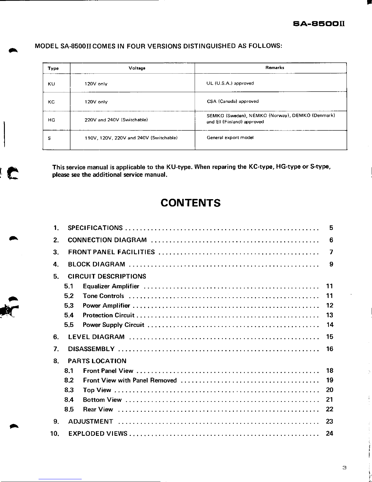
MODEL
SA-8500IICOMES
lN FOUR VERSTONS
DTSTINGUISHED
AS FOLLOWS:
re
A
This
service
manual is applicable
to the Ku-type.
When reparing the
KC-type, Hc'type or S-type,
please
see the additional service
manual.
CONTENTS
l.
2.
3.
4.
5.
6.
7.
8.
11
11
12
16
18
l9
20
CONNECTION DIAGRAM
SPECIFICATIONS
BLOCK
DIAGRAM
5,2 Tone Controls
LEVEL DIAGRAM
5
6
7
9
13
14
15
21
22
23
24
FRONT
PANEL
FACILITIES
CIRCUIT DESCRIPTIONS
5.1
EqualizerAmplifier
a.
*r:
5.3
Power
Amplifier
5.4
Protection
Circuit
5.5 Power Supply Circuit
PARTS LOCATION
8.1
Front Panel View
DISASSEMBLY
8.3 Top
View
8.5 Rear View
ADJUSTMENT
4.2 Front View with Panel Removed
8.4 Bottom
View
9.
10.
Type
Voltage
R€marks
KU
120V
only
UL
{U.S.A.)
approved
KC
120V only
CSA
(Canada)
approved
HG 22OV
and 24Ov
(Switchable)
SEMKO
(Sweden),
NEMKO
{Norway},
DEMKO
(Denmark)
and El
{Finland}
approved
s
1 1OV . 12OV . 22Ov and
24OV { Sw itch able
}
General export
model
t\
EXPLODED VIEWS
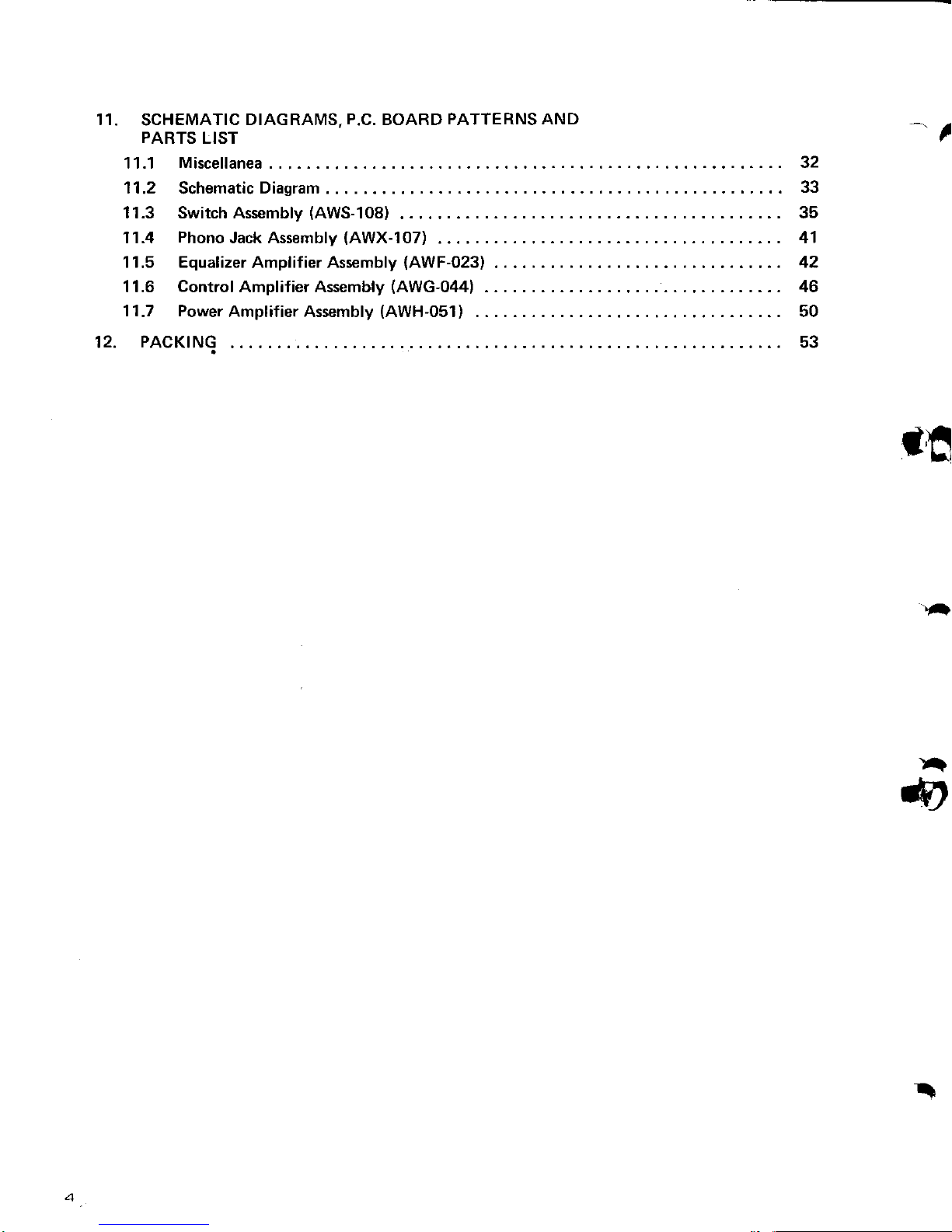
11.
SCHEMATIC
DIAGRAMS.
P.C.
BOARD
PATTERNS AND
PARTS
LIST
11.1
Miscellanea
11,2
Schematic
Diagram
.
11.3 Switch Assembly
(AWS-108)
11 .4
Phono
Jack Assembly
(AWX-I07)
1 1.5 Equalizer Amplif ier Assembly
(AWF-023)
1 1.6
Control
Amplif ier Assembly
(AWG-044)
11.7 Power
Amplif ier Assembly
(AWH-05I
)
12.
PACKING
-l
32
33
35
41
42
46
50
53
-
)a
@
\
I
a
)
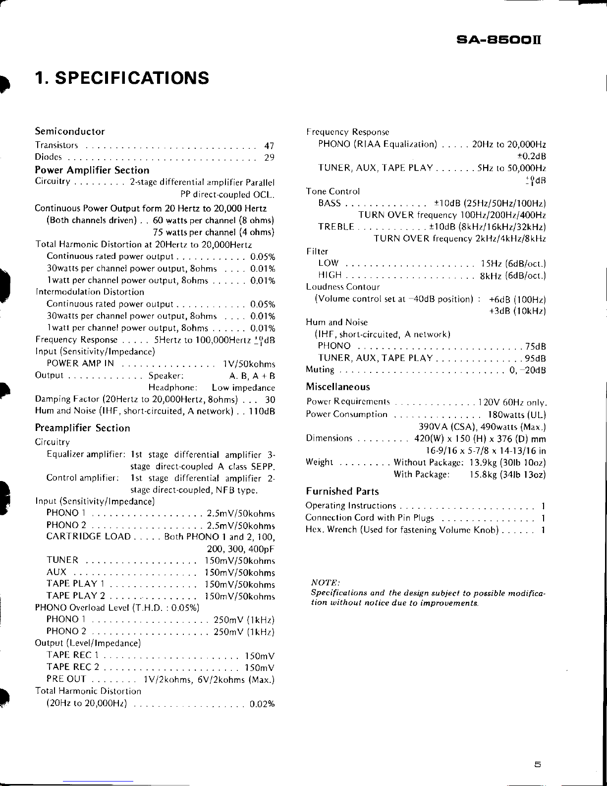
1.
SPECIFICATIONS
Semiconductor
Transistors
.....47
Diodcs..
......29
Power
Amplifier Section
Circuitry
.
2-stagc differenrial
amplifier
parallcl
PP direct-coupled
OCL.
Continuous Power
Output form 20 Hertz to 20,000 Hertz
(Both
channels driven)
. . 60
watts
per
channel
(8
ohms)
75 watts
per
channel
(4
ohms)
Total Harmonic Distortion
at 20Hertz to 20,000Hertz
Continuousratedpoweroutput
.... 0.O5o/o
3owatts
per
channcl
power
output,8ohms
. . . . 0.01y.
I watt
per
channel
power
output, 8ohms
. . . . . . 0.01%
lntermodulation Distortion
Continuous rated
power
output
. . . 0.05%
3owatts
per
channel
power
output,8ohms
. . . . 0.01%
I watt
pcr
channel
power
output, 8ohms
. . . .
. . 0.01y.
Frequency
Respon5c
.. . . . 5Hertzto 100,000Herrzl0,dB
lnput
(Sen
sitivity/
lm
pedance)
POWERAI\4PlN
.....
... 1V/5Okohms
Output..
.. Speaker:
A.B,A+B
Preamplifier
Section
Circu itry
Equalizer
amplifier: lst
stage differential
amplifier
3-
stage direct-coupled
A class SEPP.
Control amplifier: lst
stage differential
amplifier 2-
stagc direct-coupled, NFB
type.
Input
(Sensitivity/l
mpcdance)
PHONOl
.
. .
2.5mV/50kohms
PHONO2
. . . 2.5mV/50kohms
CARTRIDGE LOAD.
. . . . Both PHONO
I and 2, 100,
200,300,400pF
TUNER
.
.. 150mV/50kohms
AUX ...
.. 150mV/50kohms
TAPEPLAY1......
15OmV/5Okohms
TAPEPLAY2........
l50mV/5okohms
PHONO
Overload Level
(T.H.D.
:0.05%)
PHONO L
...250mV(1kHz)
PHONO2
....250mV(1kHz)
Output
(Level/
lm
pedance)
TAPEREC1......
150mV
TAPEREC2......
.........'l50mv
PRE
OUT
lv/2kohms,
6V/2kohms
(Max.)
Total Harmonic Distortion
(20H2
to
20,000H2)
......
..... o.o2.A
Frequency Responsc
PHONO
(RIAA
Equalization)
TUNE
R, AUX, TAPE PLAY
Filter
LOW
... ...
... .
H|GH..........
Loudness
Contou r
(Volume
control set at
sA-a5ClC'II
20Hz to 20,000H2
t0.2dB
. 5Hz to 50,000H2
j
?dB
Tone Control
BASS... ...
r10dBl25Hzl5l9zll01Hz)
TU RN OVER frequency 1Q0Hzl200Hzl4O0Hz
TREBLE.
...i10d8(8kHzl'l6k9zl32k1z)
TURN OVE R frequency 2kHzl4kHzlSkHz
... 15Hz
(6dB/oct.)
. .
8kHz
16d
B/oct.)
40dB
position) : +6dB
(100Hr)
+3dB (1okHz)
Hum
and
Noise
(lH
F,
short-circuited,
A network)
PHONO.
TUNER,
AUX, TAPE PLAY
. . .
l\4uting
..
M iscellaneous
Power
Rcquiremcnrs
120V 60Hz only.
Powcr
Consumption
l80watts
(UL)
390VA
(CSA),
490watts
(Max.)
Dimensions
. a20(W)
x 150
(H)
x
376
(D)
mm
16-9116 x 5-118 x 14-13116
in
Weighl
. . Without Package:
13.9kg
(301b
l0oz)
With
Package:
15.8kg
(341b
13oz)
Furn
ished Parts
Operating
Instructions
.......1
Connection
Cord
with
Pin Plugs
........1
Hcx. Wrench
(Used
for
fastening Volume
Knob) . . . . . .
'l
NOTE:
Specificotions
ond the design
subject to
possible
modifica-
tion
u,ithout notice due
to improuements.
...75d8
. . . 95dB
0,20d8
I
Headphone:
Low
impeddnc
c
r
Damping I dclor
(20Hert1
lo 20.000Hcrt./,
8oh m:) .
. . 30
Hum
and Noise
(lHF,
short-circuited,
A network) . . 110d8
!
p
2.
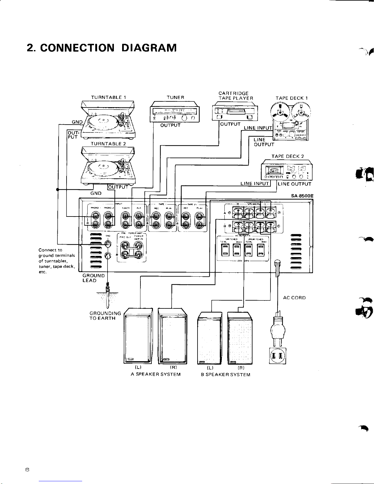
CONNECTION
DIAGRAM
TU RNTABLE 1 TUNE R
TU RNTABLE
2
'r'l
CARTRIDGE
TAPE PLAYE
R
TAPE DECK 2
JU
-n
Connect to
ground
terminals
etc.
GROUND
LEA
D
GROUNDING
TO EARTH
F
@
A SPEAKE
R SYSTEM
B SPEAKE R
SYSTEM
I
3.
FRONT
PANEL
FACILITIES
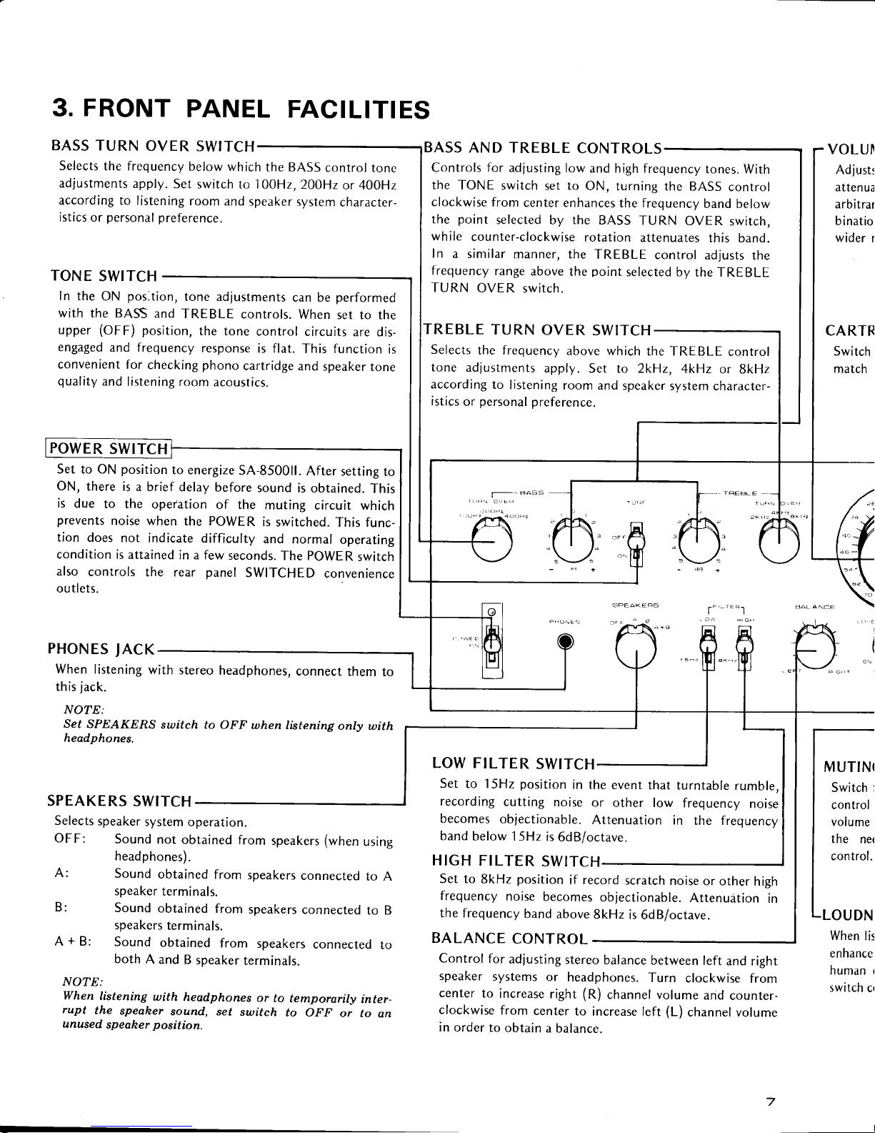
BASS TURN
OVER SWITCH
Selects
the frequency
below
which
the BASS
controt
tonc
adjustments
apply.
Ser
swirch to 100H2,
200H2
or 40OHz
according to
listening
room
and speaker
system
character-
istics or
personal preference.
TONE
SWITCH
ln the
ON
pos;tion,
tone adjustments
can be
performed
with the BASS
and
TREBLE
controls.
When
set to the
upper
(OFF) position,
the tone
control
circuits
are dis-
engaged
and frequency
response
is flat.
This function
is
convenient
for
checking
phono
cartridge
and speaker
tone
quality
and listening
room
acoustics.
Set to ON
position
to energize
54-850011.
After
setting
to
ON,
there
is a brief
delay
before
sound
is obtained.
This
is
due
to the
operation
of the
muting circuit
which
prevents
noise when
the PowER
is
switched.
This func-
tion does
not
indicate
difficulty
and
normal
operating
condition
is attained
in a few
seconds.
The POWER
switch
also
controls
the rear
panel
SWITCHED
convenience
outlets.
PHONES
JACK
When
listening
with
stereo
headphones,
connect
them
to
this
jack.
NOTE:
Set SPEAKERS
switch
to OFF
when listening
only with
headphones.
SPEAKERS
SWITCH
Selects
speaker
system
operation.
OFF:
Sound
not obtained
from
speakers
(when
using
headphones).
A:
Sound
obtained
from
speakers
connected
to A
speaker
terminals.
B:
Sound
obtained
from
speakers
connected
to B
speakers
terminals.
A+B:
Sound
obtained
from
speakers
connected
to
both
A
and B
speaker
terminals.
NOTE:
When
listening
with
headphones
or
to
temporarily
inter-
rupt
the
speaher
sound, set
switch
to OFF
or to
an
unused
speaher
position.
BASS
AND TREBLE
CONTROLS
Controls for
adlusting
low and high
frequency
tones.
With
the TONE
switch
set to ON,
turning the
BASS
control
clockwise
from
center enhances
the frequency
band below
the
point
selected
by the BASS
TURN
OVER
switch,
while
counter-clockwise
rotation
attenuates
this band.
In
a sinrilar
manner,
the
TREBLE
control
adjusts
the
frequency
range
above
the
point
selected by
the
TREBLE
TURN
OVER
switch.
TREBLE
TURN
OVER
SWITCH
Selects
the frequency
above
which
the TREBLE
control
tone adjustments
apply.
Set to
2kHz, 4kHz
or SkHz
according
to
listening
room and
speaker
system character-
istics
or
personal
preference.
t'-""1
LOW FILTER
SWITCH
Set
to 15Hz
position
in the
event
that turntable
rumble.
recording
cutting
noise
or
other low
frequency
noise
becomes
ob
jectionable.
Attenuation
in
the frequency
band
below
15Hz
is
6dB/octave.
HIGH
FILTER
SWITCH
Set
to 8kHz
position
if record
scratch
noise
or other
high
frequency
noise
becomes
objectionable.
Attenudtion
in
the frequency
band
above
8kHz
is
6dB/octave.
BALANCE
CONTROL
Control
for
adjusting
stereo
balance
between
left
and right
speaker
systems
or
headphones.
Turn
clockwise
from
center
to
increase
right
(R)
channel volume
and
counter-
clockwise
from
center
to
increase
left
(L)
channel volume
in
order
to obtain
a balance.
VOLUI
Adf
usts
atten
ua
arbitrar
b inatior
wider
r
CARTR
Switch
match
I{
t--
I
MUflN(
I
Switch I
I
control
I
volume
I
the ne(
I
controt.
I
I
LLOUDN
When
lis
enhance
numan
(
switch
c(
7
POWER
SWITCH
lones.
With
SS control
)and below
5R
switch,
this band.
idjusts
the
E TREBLE
LE
control
z or
8kHz
I character-
f'-"''r
able rumble,
uency
noise
e frequency
rr other
high
tenuition
in
left
and right
ckwise from
and counterlnnel volume
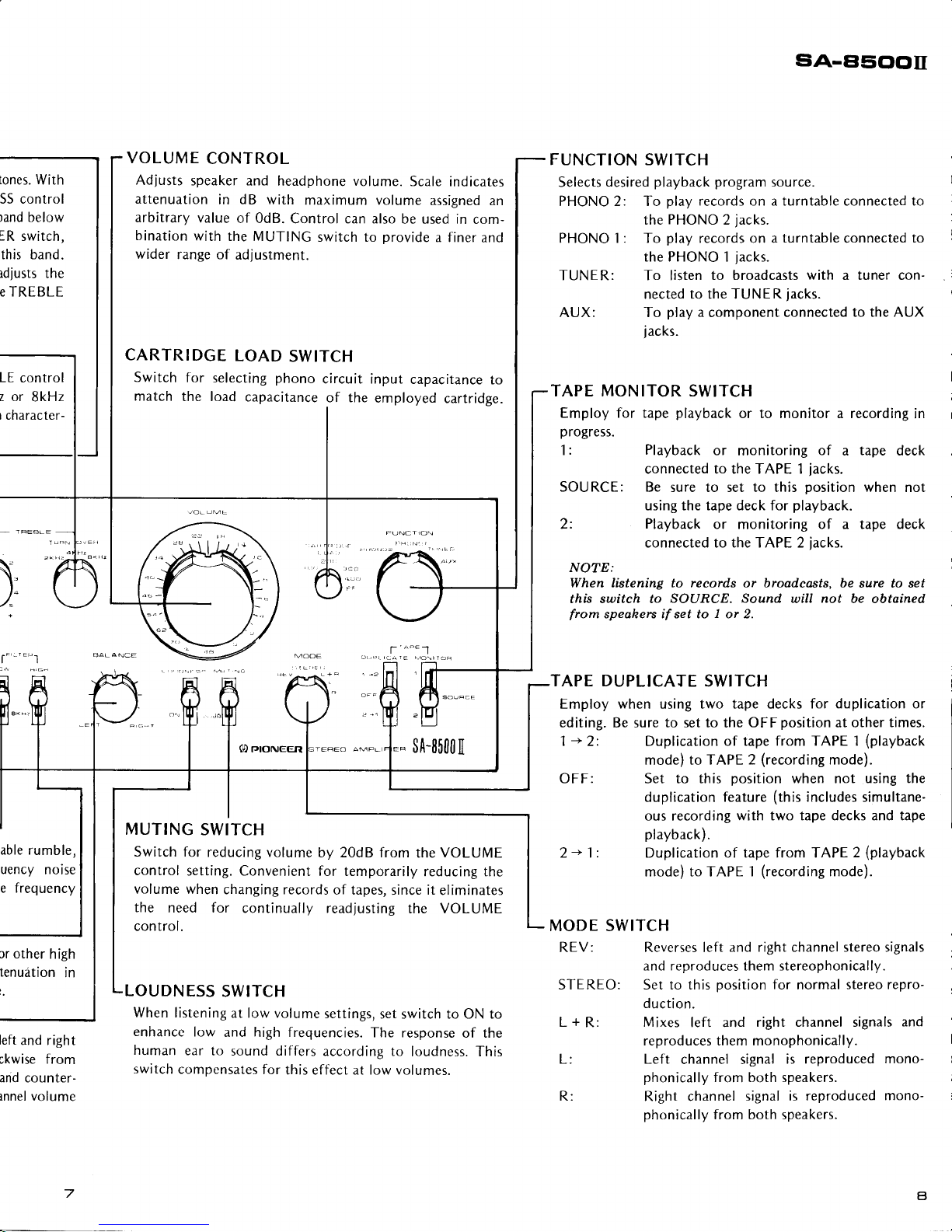
CARTRIDGE
LOAD
SWITCH
Switch
for
selecting
phono
circuit
match
the load
capacitance
of the
input
capacitance
to
employed
cartridge.
VOLUME
CONTROL
Adlusts
speaker
and headphone volume.
Scale
indicates
attenuation
in dB with
maximum
volume
assigned an
arbitrary
value
of 0dB.
Control can also
be used in
com-
bination
with
the MUTING
switch to
Drovide
a finer
and
wider
range of
adjustment.
sA-A5Clcltr
FUNCTION SWITCH
Selects
desired
playback program
source.
PHONO 2: To
play
records on a turntable connected to
the
PHONO
2
jacks.
PHONO 1 : To
play
records on a
turntable
connected
to
the PHONO
1
iacks.
TUNER: To listen
to broadcasts
with
a tuner con-
nected to the TUNER
iacks.
AUX: To
play
a
component
connected to the AUX
iacks.
TAPE MONITOR SWITCH
Employ for tape
playback
or to monitor a recording
in
progress.
1
: Playback
or monitoring
of a tape
deck
connected to the TAPE 1
jacks.
SOURCE:
Be sure to set to this
position
when not
using the tape deck for
playback.
2:
Playback
or
monitoring
of a tape deck
connected to the TAPE 2
iacks.
NOTE:
When listening to records or broadcasts, be
sure to set
this switch to
SOURCE. Sound
will
not
be obtained
from
speahers if set to I or 2.
TAPE DUPLICATE
SWITCH
Employ when using two tape decks for
duplication or
editing. Be sure
to set to
the
OFFposition at other times.
1
-->
2: Duplication of tape
from TAPE 1
(playback
mode)
to T APE 2
(recording
mode).
OFF:
)
T'"-'-l
(0
rrrorueen
IEREO AMPL
$A-8500
[
MUTING
SWITCH
Switch for
reducing volume
by 20dB from
the
VOLUME
control
setting. Convenient
for temporarily
reducing the
volume when
changing records
of tapes,
since
it
eliminates
the
need for
continually read
justing
the VOLUME
control.
OUDNESS
SWITCH
When listening
at low volume
settings,
set switch to ON to
enhance
low
and high frequencies.
The response
of the
human
ear
to sound differs
according to
loudness. This
switch
compensates
for
this effect at low volumes.
Set to this
position
when not using
the
duplication feature
(this
includes simultane-
ous recording
with two tape decks and tape
playback).
Duplication of tape from TAPE
2
(playback
mode) to TAPE 1
(recording
mode).
SWITCH
Reverses left
and right channel stereo signals
and reproduces them stereophonically.
2- 1:
MODE
REV:
STEREO: Set to this
position
for
normal
stereo repro-
duction.
L
+
R:
Mixes
left and
right channel signals
and
reproduces them monophonically.
L: Left
channel signal
is reproduced
mono-
phonically
from both speakers.
R:
Right channel
signal is
reproduced
mono-
phonically
from both speakers.
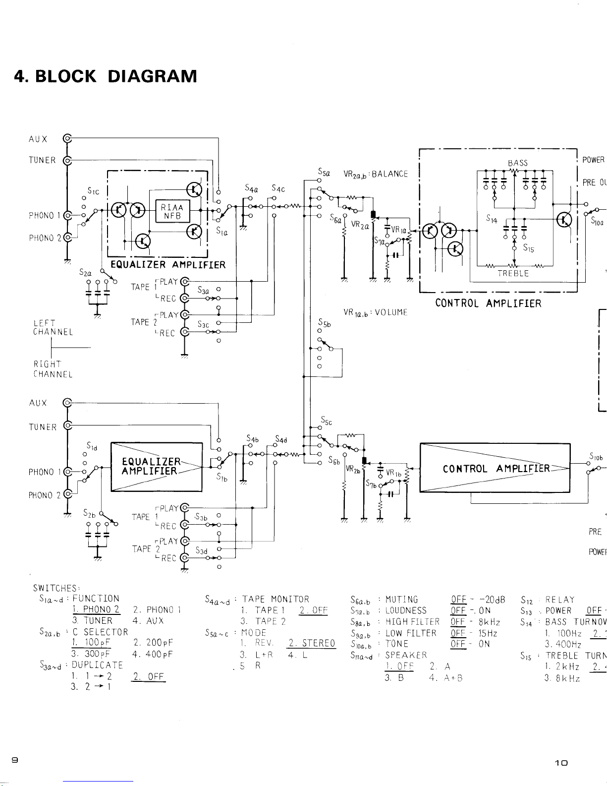
4. BLOCK
DIAGRAM
Ssa
o
S+a-d ' TAPE
MONITOR
1. TAPEI 2 OFF
3.
TAPE
2
Ssa-c
,X0DE
1
REV
3.
LrR
.5
R
2
STEREO
I oncc
I
POwrn
BA
SS
PRE
OL
TREBLE
CONTROL
AMPLIFIER
l-
L
PRE
POWEF
tt
SV'JITCH ES
,
Sra-d'FUNCTI0N
t.
PH0N0
2
3
TUNER
Szo,b,C
SELECIOR
1.
100pF
3.
300pF
S3o-d,DUPLICATF
l.
l*2
3.2*1
sqc
s+a
Ssa
VRza,b
,
BA
LANCE
VR
ra,u'
V0 LUIIE
6
VRru
c^
rbo,b
Sra,
s
Sao,
u
Sso,
o
Stoo,
u
'
IlUTI NG
:
TOUDNESS
'
HIGH
FITIER
'
LOW
FILTER
.TONE
'SPEAKER
]
OFF
?
3 B 4.
OFF
- -20d8
OFF
_.
ON
OFF
-
BkHz
OFF
15 Hz
OrF - 0N
A
A+B
Srz
RE
LAY
S13
.
POWER OFF
-
S1a
'
BASS TUR N 0V
I
100H2
7.',
a / ^^ |
J..tLrul.'17
Sl5,TREBLE
TURN
1.
Tk\z
l.
z
3
BkHz
PHONO
1
PH(')NO
2
AUX
TU
N FR
LEFT
CHANNEL
RIGHT
CFIANNET
EQUALIZER
AI'lPLIFIER
"l
-"
1t1
v
TAPE
|PLAY
LREc
-
PLAY
TAPE
2
LREC
J
q^^
Sno
5+u
"9
o6b
I
I
vRto
I
c
J2i)
.PLAY
TAPE
1
.REC
.
PL A'l
TAPE 2
LREC
2 . Pr-10N0
1
4.
AUX
2
200pF
4.
400pF
2. OFF
EQUA
LIZER
AIlPLIFIER
CONTROL
AHPLIFIER
4
L
Srra-a
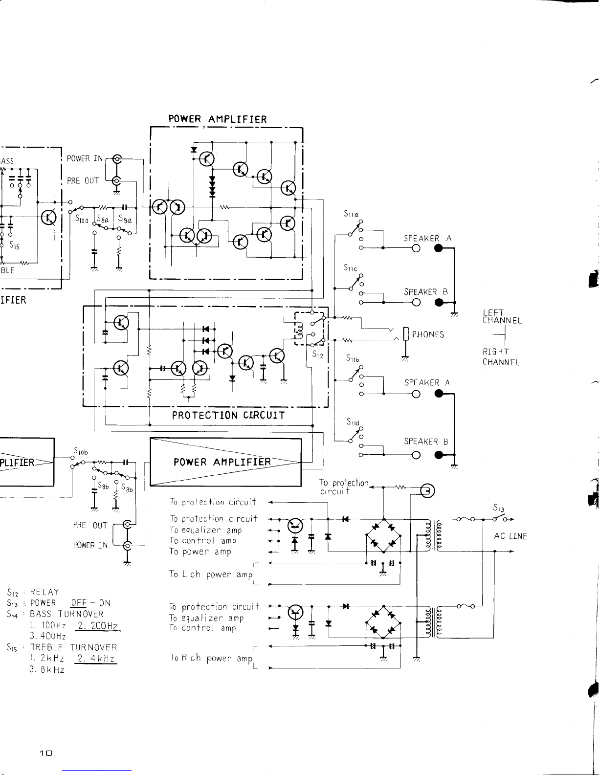
.
RE
LAY
..
POIIER OFF
-
ON
.
BASS TURNOVER
1.
l00Hz
2.200H2
3.400H2
TREBLF
TURNOVER
1.
LkHz
2. 4kl,z
3.
BkHz
PO
r-
WER
AI1PLTFIER
L
PROTECTION
CIRCUIT
To
pnotection
clr^cuit
To
pnotection
cir cuit
To equalizer^
amp
To
con
f
r-o I
amp
To powen
amp
r
To
L
ch
powen ampl
proteclron
cir cuit
eguallzen
amP
Contr0
I
amP
T
To
R
ch
powen ampL
e
u9o
c
JIo
o
8a
ls
I
T
J
J
T
FIER
LEFT
CHANN
EL
I
I
RIG HT
CHANNEL
f
rloru,s
SPEAKFR A
?e
*
"sb
I
e
ISeu
T
I
)-
PRE
OUT
POWER
IN
To
pr
otection
cir-cuit
;
I
c
e13
CP
AC
LTNE
Srz
Srs
a
u14
r0
To
To
i
I
i
I
,
POWER
AIlPLIFIER
Srs
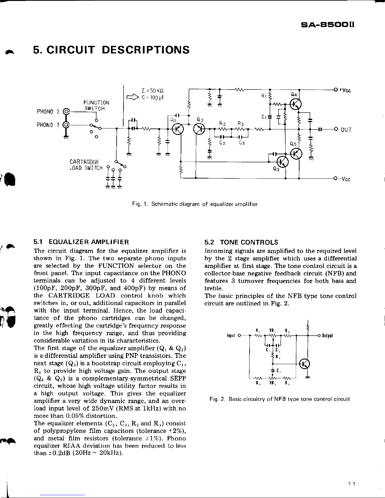
A
5. CIRCUIT
DESCRIPTIONS
z=50Krt
c)
c=roopr
PHONO
2
PHONO
I
CARTRIDGE
LOAD SWITCH
sA-El5ClClII
-vcc
+
lr.
rl
Fig.
L Schematic diagram
of equalizer amplifier
,li
5.1 EOUALIZER
AMPLIFIER
The
circuit
diagram for the equalizer amplifier is
shown in Fig. 1.
The
two separate
phono
inputs
are selected by the
FUNCTION selector on
the
front
panel.
The input capacitance
on
the PHONO
terminals can be adjusted to 4
different
levels
(100pF,
200pF, 300pF, and 400pF) by means of
the
CARTRIDGE LOAD control knob
which
switches in,
or out, additional capacitors in
parallel
with the input terminal. Hence, the load capacitance of the
phono
cartridges can be changed,
greatly
effecting
the cartridge's frequency response
in the high frequency
range, and thus
providing
considerable variation in its characteristics.
The first stage
of the
equalizer
amplifier
(Q'
&
Qr)
is
a differential amplifier using PNP transistors. The
next stage
(Q.)
is a bootstrap circuit employing
C'
,
R1 to
provide
high voltage
gain.
The output stage
(Qo
&
Qr)
is a complementary-symmetrical
SEPP
circuit, whose high voltage
utility
factor
results
in
a high
output voltage. This
gives
the equalizer
amplifier a
very wide dynamic range, and an over-
Ioad input level
of 250mV
(RMS
at lkHz) with no
more than 0.05% distortion.
The equalizer elements
(Cr,
C.,,
R,
and
R.)
consist
of
polypropylene
film capacitors
(tolerance 127o),
and metal frlm resistors
(tolerance
t1%).
Phono
equalizer
RIAA
deviation has been
reduced
to less
than
10.2dB
(2OHz
-
2OkHz\.
5.2
TONE
CONTROLS
Incoming
signals are amplified to the required level
by
the 2 stage amplifier
which
uses a differential
amplifier at first stage. The tone control circuit is a
collector-base negative
feedback
circuit
(NFB)
and
features 3
tumover frequencies for both
bass
and
treble.
The
basic
principles
of the NFB type tone control
circuit are outlined in Fis. 2.
'fl
h
rl
0d0ut
hI|lt
n, vn,
n,
L.-
,,,
-{P
c.
Rl
,c.
d
Fi1. 2.
t, vR, R,
Basic circuitry of
NFB
type tone control circuit
iri
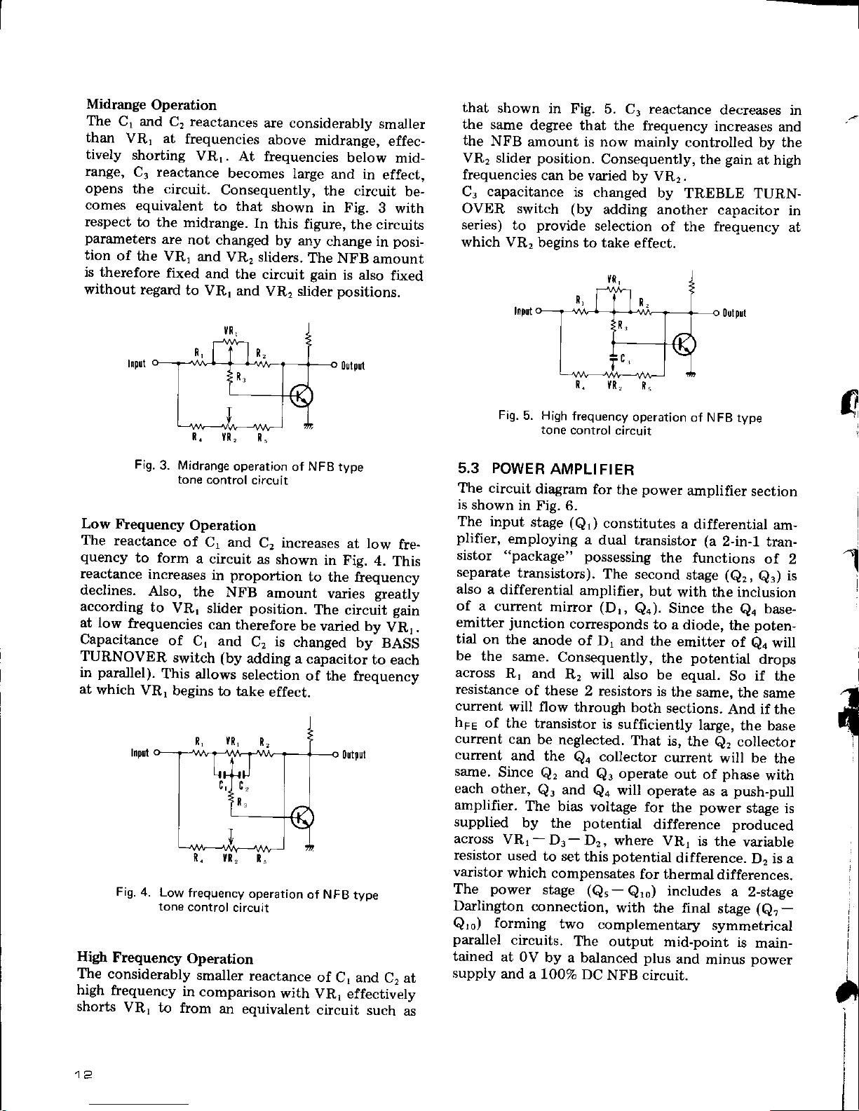
Midrange
Operation
The
Cr and
C, reactances
are considerably
smaller
than
VRr at
frequencies
above
midrange,
effec-
tively
shorting
VRr.
At frequencies
below
mid-
range,
C. reactance
becomes
large
and in
effect,
opens
the circuit.
Consequently,
the circuit
be-
comes
equivalent
to that
shown
in Fig.
3
with
respect
to the
midrange.
In
this
figure,
the circuits
parameters
are
not changed
by any
change in
pos!
tion
of the
VR, and
VR.
sliders.
The NFB
amount
is therefore
fixed
and
the circuit gain
is also
fixed
without
regard
to VRr
and
VR, slider
positions.
Fig.
3. Midrange
operation
of
NFB
type
tone control
circuit
Low Frequency
Operation
The
reactance
of
C, and
C, increases
at low
fre-
quency
to form
a circuit
as
shown
in Fig.
4.
This
ipactance
increases
in proportion
to the
frequency
declines.
Also,
the
NFB
amount
varies
grea
y
according
to
VR1
slider
position.
The
circuit
sain
at low
frequencies
can therefore
be
varied by
Vh1.
Capacitance
of
C1 and
C,
is
changed
by BASS
TURNOVER
switch
(by
adding a
capacitor
to each
in
parallel).
This
a.llows
selection
of the
frequencv
at
which
VR, begins
to take
effect.
that
shown
in Fig.
5. C. reactance
decreases in
the
same
de$ee that
the frequency
increases
and
the
NFB
amount is now mainly
controlled by the
VR, slider
position.
Consequently,
the
gain
at high
frequencies
can be
varied by
VR:.
C. capacitance
is changed
by
TREBLE TURN-
OVER switch
(by
adding another
capacitor
in
series)
to
provide
selection
of the frequency
at
which
VR: begins
to take
effect.
Fiq.
5. High
frequency
operation
of NFB
type
tone
control
circuit
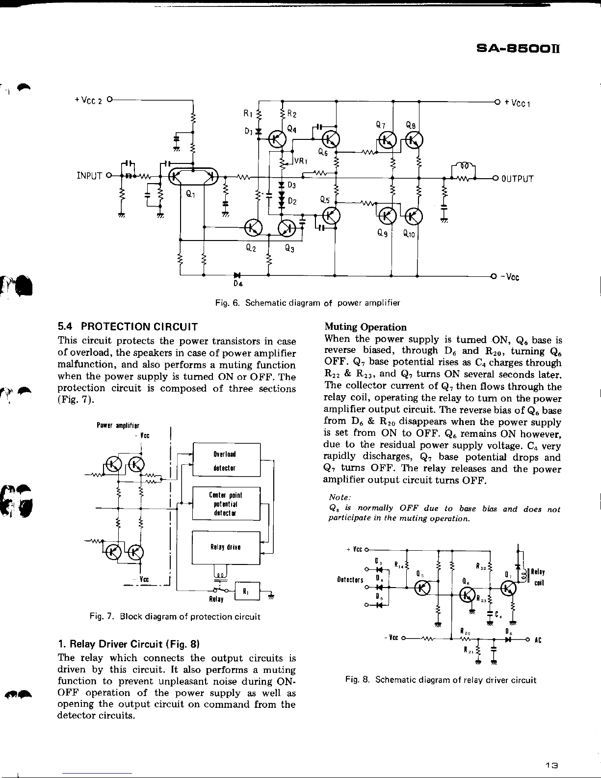
5.3 POWER
AMPLIFIER
The circuit
diagram
for the
power
amplifier
section
is
shown
in
Fig. 6.
The input
stage
(Q1)
constitutes
a
differential
am-
plifier,
employing
a
dual transistor (a
2-in-1
tran-
sistor
"package"
possessing
the
functions
of
2
separate
transistors).
The
second
stage
(er,
e.)
is
also
a differential
amplifier,
but
with the inclusion
of a
current
mirror
(D1,
Qr).
Since the
ea
base-
emitter
junction
conesponds
to a diode,
the
poten-
tial
on the
anode
of D,
and the
emitter
of
eo
will
be
the same.
Consequently,
the
potential
drops
across
R, and
R, will
a.lso be
equal.
So if the
resistance
of these
2 resistors
is
the same,
the same
current
will flow
through
both
sections.
And if the
hpg
of
the transistor
is sufficiently
large,
the base
current
can
be
neglected.
That
is, the
e.
collector
current
and
the
Qa
collector
current
will
be
the
same.
Since
Q,
and
Q3
operate
out
of
phase
with
each
other,
Q:
and
Qo
will
operate as
a
push-pull
amplifier.
The bias
voltage
for
the
power
stage
is
supplied
by
the
potential
difference produced
across
VR1
-
D3
-
D,
,
where VR1
is the
variable
resistor
used to
set this
potential
difference.
D, is a
varistor
which
compensates
for thermal
differences.
The
power
stage
(Qs-
Q16)
includes
a 2-stage
Darlington
connection,
with
the fina.l
stage
(e7-
Qto)
forming
two
complementary
symmetrical
parallel
circuits.
The
output
mid-point is
main-
tained
at 0V
by a balanced plus
and
minus
power
supply
and
a 700%
DC
NFB circuit.
f
)
I
'l
l
fr
vn.
Fig.
4. Low
frequency
operation
of NFB
type
tone
control
circuit
High
Frequency
Operation
The considerably
smaller
reactance
of
C, and
C" at
high
frequency
in
comparison
with
VR,
effectivelv
shorts
VR,
to
from
an
equivalent
circuit
such
as
-r
''r
i
sA-aE'ootr
+vcc1
OUTPUT
+vcc2
INPUT
ft.'f
r\i'^
5.4 PROTECTION
CIRCUIT
This circuit
protects
the
power
transistors in
case
of
overload, the speakers
in case
of
power
amplifier
malfunction,
and also
performs
a
muting function
when the
power
supply is tumed
ON or
OFF. The
protection
circuit is composed
of three sections
(Fis.7).
Por!r.r||0lili!r
Fig. 7.
Block diagram
of
protection
circuit
1. Relay Driver
Circuit
(Fig.
8l
The
relay which connects
the output circuits is
driven
by this circuit. It
also
performs
a muting
function
to
prevent
unpleasant noise during
ON-
OFF operation
of the
power
supply
as well as
opening the
output circuit on command
from the
detector
circuits.
04
Fig. 6. Schematic diagram
of
power
amplifier
Muting
Operation
When the
power
supply
is
tumed
.ON,
Qu
base is
reverse biased,
through
D6 and
R26, turning
Qo
OFF.
Q?
base
potential
rises
as Ca charges
through
R22 & Rz3, and
Q?
turns
ON several
seconds
later.
The collector
current
of
Q7
then
flows
through
the
relay coil,
operating
the
relay to tum
on the
power
amplifrer
output circuit.
The
reverse bias
of
eu
base
from
Du
&
R2o
disappears
when the
power
supply
is set
from
ON to
OFF.
Qu
remains
ON however,
due
to the residual power
supply
voltage. Ca
very
rapidly
discharges,
Q,
base
potential
drops
and
Q?
tums
OFF.
The relay
releases
and the
power
amplifier
output
circuit
turns
OFF.
Note:
Q"
is
normally
OFF due
to base
bias
and does
not
participate
in
the
muting operction.
{tr-
Fig.
8. Schematic diagram
of relay driver circuit
Operation by Detector
Circuit Command
Command from
the detector
circuits
pass
through
one of D., Do or
D, and are applied in the form
of
a current
flow.
Q5
is normally
reverse biased
through
R1a,
but
when a large current flows
through
on of these diodes,
Q,
base
potential
declines according
to the voltage drop
at R,a.
Q,
then
becomes
ON,
Qu
base
potential
rises and
Qu
becomes
ON. Co rapidly
discharges and
Q,
base
potentia.l
drops, tuming
Q?
OFF. The relay
releases
and the
power
amplifier output circuit
becomes cut
off.
2.
Overload Detecto? Circuit
Shorting
of the
power
amplifier load
or a load
impedance
below the specified
value causes a
command
to be sent to
the relay drive circuit.
This is illustrated
in Fig.
9.
Qa
emitter is connected
to
Q,
base
through
R,
and
the
junction
point
to
Q,
emitter.
When
RL
is
extremely small, Iarge current flows
in
Qa, Q,
turns
ON
due
to the
RE,
voltage
drop, and current flows
in
D.. C1
prevents
faulty operation
due to extemal
norse.
oirplifier
eq
Fig.
9. Basic
circuitry
of
overload detector
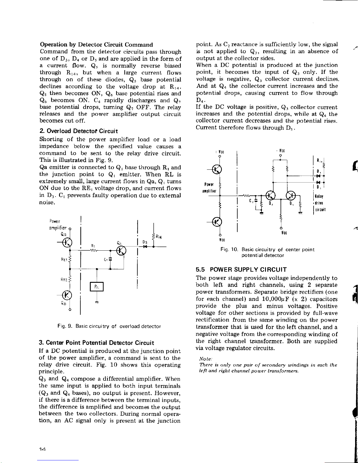
3. Center Point Potential
Detector Circuit
If
a DC
potential
is
produced
at the
junction
point
of the
power
arnplifier, a
command is sent to the
relay drive circuit.
Fig. 10 shows
this operating
principle.
Qr
and
Qo
compose
a differential amplifier.
When
the
same input is
applied to both input
terminals
(Q.
and
Qo
bases),
no
output
is
present.
However,
if there
is a difference between
the terminal inputs,
the
difference is amplified
and becomes the
output
between
the two collectors.
During normal
opera-
tion, an
AC signal only is
present
at the
junction
point.
As Cr reactance is
sufficiently
low,
the signal
is not applied to
Q3,
resulting in
an
absence of
output at the collector sides.
When a DC
potential
is
produced
at the
junction
point,
it becomes
the input of
Q.
only. If the
voltage
is negative,
Q.
collector current declines.
And at
Qo
the collector current increases and the
potential
drops, causing current to flow through
If the
DC voltage is
positive,
Q.
collector
current
increases
and
the
potential
drops,
while at
Qo
the
collector current
decreases
and
the
potential
rises.
Current therefore flows
through D. .
Fig- 10.
Basic circuitry
of
center
point
potential
detector
5.5 POWER SUPPLY
CIRCUIT
The
power
stage
provides
voltage
independently
to
both left
and right channels, using 2 separate
power
transformers.
Separate
bridge
rectifiers
(one
for each
channel) and 10,000gF
(x
2) capacitors
provide
the
plus
and
minus voltages. Positive
voltage for
other
sections
is
provided
by full-wave
rectification from the same
winding on the
power
transformer
that is used for
the
left
channel, and a
negative
voltage from the corresponding
winding of
the right channel
transformer. Both are supplied
via voltage
regulator circuits.
There
is only one
pair
of
secondary
windings in each
the
lcfl and righl
channel
powcr
lrans[ormcrs.
t
{
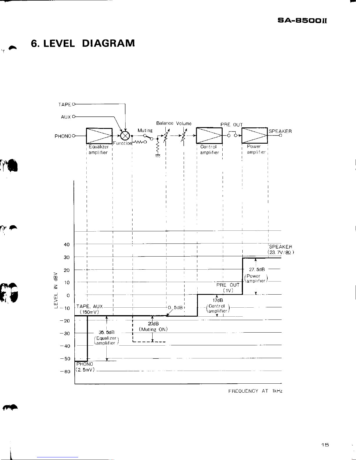
6.
LEVEL
DIAGRAM
siA-E'5clclil
SPEAKER
't
A
PRE
OUT
PRE OUT
(
1V)
-
-SPEAKEF
(23.7v,
&) )
amp 1er
f\il
|
[*i
.D
1
d
J-
20
10
0
10
-20
30
50
-60
27. 5dB
/Power l
\afn0lrlrer/
lf
35.5dB
iEqual
zer
\
\amplrfrer
/
r
(Muting
ON)
17d B
APL. AU\
.r0 5oB
/r5O,rV)
./
/Control \
\am
plif
re r
/
(2.
5mv)
tzel
I rer
FREOUENCY
AT lKHZ
rtf
7.
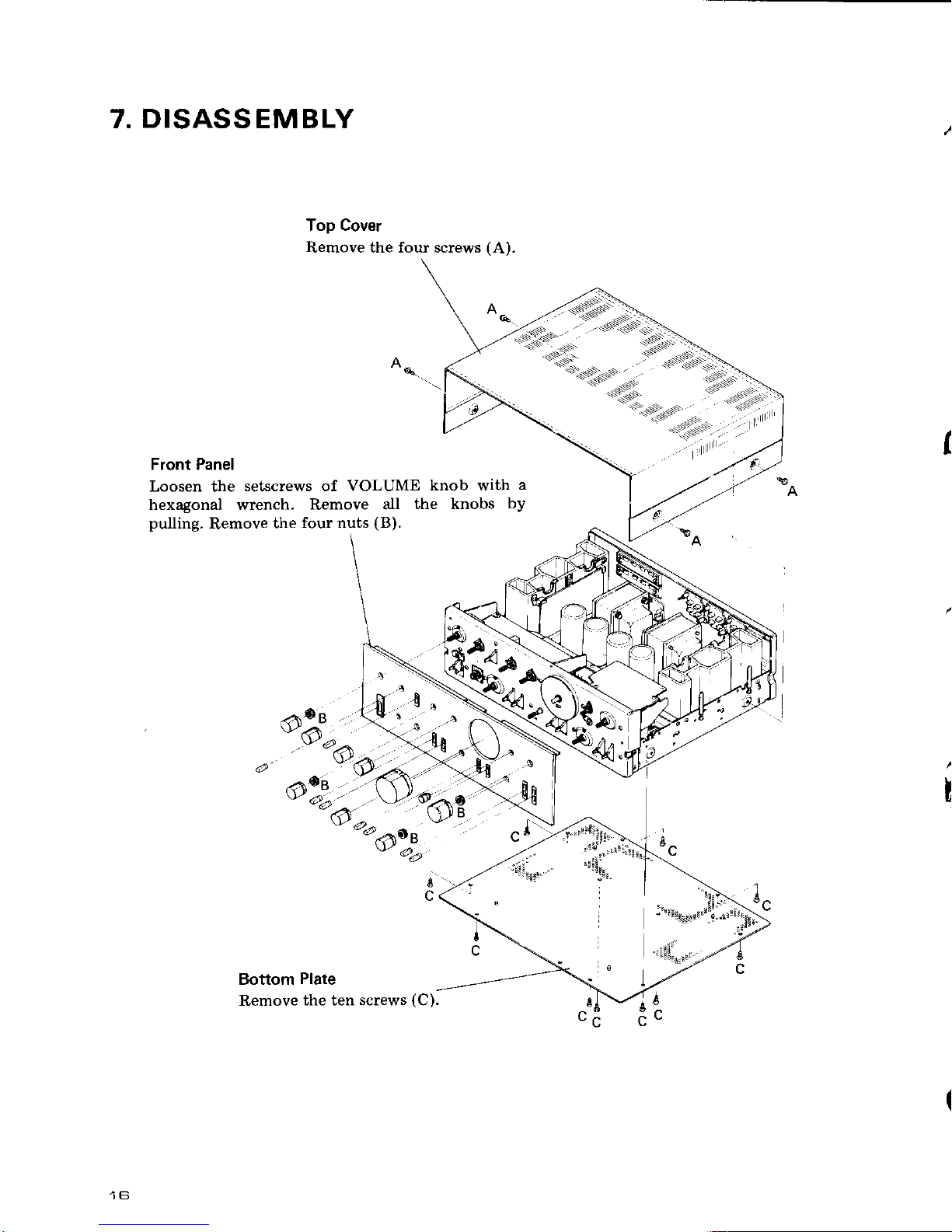
DISASSEMBLY
Top Cover
Remove the four screws
(A).
Front Panel
Loosen the
setscrews of VOLUME
knob with
a
hexagonal wrench. Remove
all
the knobs
by
pulling.
Remove
the
four nuts
(B).
Bottom
Plate
Remove
the ten screws
(C).

Control Amplifier Assembly
Remove
the
three screws
(D).
Power Amplifier
Block
(L)
Remove
the
three
screws
(E).
CtA-E'5clC'tr
Power Amplif
ier
Block
(Rl
Remove
the
three screws
(F).
Equalizer
Amplif ier Assembly
R€move
the two
screws
(G).
Switch Assembly
Remove
the seven screws
(H).
17
 Loading...