

Page 1
PIONEER CORPORATION 4-1, Meguro 1-Chome, Meguro-ku, Tokyo 153-8654, Japan
PIONEER ELECTRONICS (USA) INC. P.O.Box 1760, Long Beach, CA 90801-1760 U.S.A.
PIONEER EUROPE NV Haven 1087 Keetberglaan 1, 9120 Melsele, Belgium
PIONEER ELECTRONICS ASIACENTRE PTE.LTD. 253 Alexandra Road, #04-01, Singapore 159936
C PIONEER CORPORATION 2003
K-ZZW. MAY 2003 Printed in Japan
ORDER NO.
CRT3107
16:9 TOUCH PANEL DISPLAY
AVD-W6210UC, EW
AVD-W6210/UC
- This product has the unit part numbers as below.
Unit Part No. Description
CPN1867 Monitor Assy(AVD-W6210/UC)
CPN1879 Power Supply Assy(AVD-W6210/UC)
CPN1857 Monitor Assy(AVD-W6210/EW)
CPN1858 Power Supply Assy(AVD-W6210/EW)
*)The unit part numbers listed above are not for the service components.
For details, refer to "Important symbols for good services".
Page 2
2
1
234
12
34
F
E
D
C
B
A
AVD-W6210/UC
SAFETY INFORMATION
[ Important symbols for good services ]
In this manual, the symbols shown-below indicate that adjustments, settings or cleaning should be made securely.
When you find the procedures bearing any of the symbols, be sure to fulfill them:
2. Adjustments
To keep the original performances of the product, optimum adjustments or specification confirmation is indispensable.
In accordance with the procedures or instructions described in this manual, adjustments should be performed.
3. Cleaning
For optical pickups, tape-deck heads, lenses and mirrors used in projection monitors, and other parts requiring cleaning,
proper cleaning should be performed to restore their performances.
5. Lubricants, glues, and replacement parts
Appropriately applying grease or glue can maintain the product performances. But improper lubrication or applying
glue may lead to failures or troubles in the product. By following the instructions in this manual, be sure to apply the
prescribed grease or glue to proper portions by the appropriate amount.For replacement parts or tools, the prescribed
ones should be used.
4. Shipping mode and shipping screws
To protect the product from damages or failures that may be caused during transit, the shipping mode should be set or
the shipping screws should be installed before shipping out in accordance with this manual, if necessary.
1. Product safety
You should conform to the regulations governing the product (safety, radio and noise, and other regulations), and
should keep the safety during servicing by following the safety instructions described in this manual.
CAUTION
This service manual is intended for qualified service technicians; it is not meant for the casual do-it-yourselfer.
Qualified technicians have the necessary test equipment and tools, and have been trained to properly and safely repair
complex products such as those covered by this manual.
Improperly performed repairs can adversely affect the safety and reliability of the product and may void the warranty.
If you are not qualified to perform the repair of this product properly and safely, you should not risk trying to do so
and refer the repair to a qualified service technician.
W
ARNING
This product contains lead in solder and certain electrical parts contain chemicals which are known to the state of
California to cause cancer, birth defects or other reproductive harm.
Health & Safety Code Section 25249.6 - Proposition 65
Page 3

3
5
6
7
8
F
E
D
C
B
A
5
6
7
8
AVD-W6210/UC
CONTENTS
SAFETY INFORMATION................................................................................................................2
1. SPECIFICATIONS ...........................................................................................................................4
2. EXPLODED VIEWS AND PARTS LIST ..........................................................................................6
2.1 PACKING(AVD-W6210/UC)...................................................................................................6
2.2 PACKING(AVD-W6210/EW)..................................................................................................8
2.3 EXTERIOR(1)(AVD-W6210/UC) ..........................................................................................10
2.4 EXTERIOR(1)(AVD-W6210/EW)..........................................................................................12
2.5 EXTERIOR(2) .......................................................................................................................14
3. BLOCK DIAGRAM AND SCHEMATIC DIAGRAM ......................................................................16
3.1 BLOCK DIAGRAM...............................................................................................................16
3.2 MONITOR PCB (PICTURE PROCESSING)(GUIDE PAGE).................................................22
3.3 MONITOR PCB (INVERTER)...............................................................................................28
3.4 KEYBOARD PCB..................................................................................................................33
3.5 MOTHER UNIT(GUIDE PAGE)............................................................................................34
3.6 DETACH UNIT(AVD-W6210/EW)........................................................................................41
4. PCB CONNECTION DIAGRAM....................................................................................................42
4.1 MONITOR PCB....................................................................................................................42
4.2 MOTHER UNIT....................................................................................................................46
4.3 KEYBOARD PCB..................................................................................................................50
4.4 DETACH UNIT(AVD-W6210/EW)........................................................................................51
5. ELECTRICAL PARTS LIST............................................................................................................52
6. ADJUSTMENT.............................................................................................................................61
6.1 POWER SUPPLY ASSY SECTION ADJUSTMENT............................................................61
6.2 MONITOR ASSY SECTION ADJUSTMENT ......................................................................63
6.3 TOUCH PANEL TEST MODE..............................................................................................71
6.4 SINGLE OPERATION MODE ..............................................................................................73
7. GENERAL INFORMATION...........................................................................................................74
7.1 DIAGNOSIS.........................................................................................................................74
7.1.1 DISASSEMBLY...........................................................................................................74
7.1.2 CONNECTOR FUNCTION DESCRIPTION.................................................................76
7.2 IC..........................................................................................................................................78
7.3 OPERATIONAL FLOW CHART............................................................................................84
8. OPERATIONS ...............................................................................................................................85
Page 4

4
1
234
12
34
F
E
D
C
B
A
AVD-W6210/UC
1. SPECIFICATIONS
- AVD-W6210/UC
General
Power source ................................................................. 14.4 V DC (10.8 — 15.1 V × allowed)
Grounding system ........................................................... Negative type
Max. current consumption .............................................. 1.5 A
Display Unit
Screen size/Aspect ratio .................................................. 6.5 inch wide/16:9
(effective display area: 154 × 87 mm)
Pixels ............................................................................. 336,960 (1,440 × 234)
Type ............................................................................. TFT active matrix, transmissive type
Color system ................................................................... NTSC/PAL compatible
Operating temperature range ........................................... –10 — +50 °C [+14 to 122F°]
Storage temperature range ............................................... –20 — +80 °C [–4 to 176F°]
Built-in Speaker ............................................................... ø 36 mm [1 - 318in]
Dimensions .................................................................... 188 (W) × 114 (H) × 32 (D) mm
[6 - 3/8 (W) × 4 - 1/2 (H) × 1 - 1/4 (D) in.]
Weight ......................................................................... 469 g (1.0lbs)
Hide-away Unit
External video input level ................................................ 1 Vp-p/75 Ω
External audio input level ................................................. 1 V/22 kΩ
Max. output impedance .................................................... 1 Vp-p/75 Ω
External audio max. output level ...................................... 1 V/1 kΩ
Dimensions .................................................................... 162 (W) × 38 (H) × 85 (D) mm
(excluding protruding parts)
[6 - 3/8 (W) × 1 - 1/2 (H) × 3 - 1/4 (D) in.]
Weight ................................................................................ 440 g (1.0 lbs)
Note:
• The specifications and design are subject to change without prior notice. Products purchased may differ in
details from illustrations in this manual.
Backup current ................................................................. 1 mA or less
Page 5

5
5
6
7
8
F
E
D
C
B
A
5
6
7
8
AVD-W6210/UC
- AVD-W6210/EW
General
Power source ................................................................. 14.4 V DC (10.8 — 15.1 V × allowed)
Grounding system ........................................................... Negative type
Max. current consumption ............................................... 1.5 A
Backup current ................................................................. 1 mA or less
Display Unit
Screen size/Aspect ratio ................................................
6.5 inch wide/16:9
(effective display area: 154 × 87 mm)
Pixels ..................................................................................
336,960 (1,440 × 234)
Type ..................................................................................
TFT active matrix, transmissive type
Color system .....................................................................
NTSC/PAL compatible
Operating temperature range .........................................
–10 — +50 °C
Storage temperature range .............................................
–20 — +80 °C
Built-in Speaker .................................................................
ø 36 mm
Dimensions ......................................................................
188 (W) × 114 (H) × 37 (D) mm
Weight ............................................................................
467 g
Hide-away Unit
External video input level ...............................................
1 Vp-p/75 Ω
External audio input level ...............................................
1 V/22 kΩ
Max. output impedance ..................................................
1 Vp-p/75 Ω
External audio max. output level ....................................
1 V/1 kΩ
Dimensions .......................................................................
162 (W) × 38 (H) × 85 (D) mm (excluding protruding parts)
Weight ............................................................................
440g
Note:
• The specifications and design are subject to change without prior notice. Products purchased may differ in
details from illustrations in this manual.
Page 6
6
1
234
12
34
F
E
D
C
B
A
AVD-W6210/UC
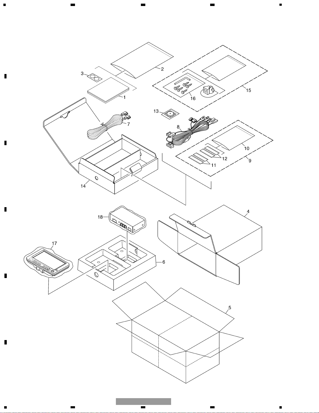
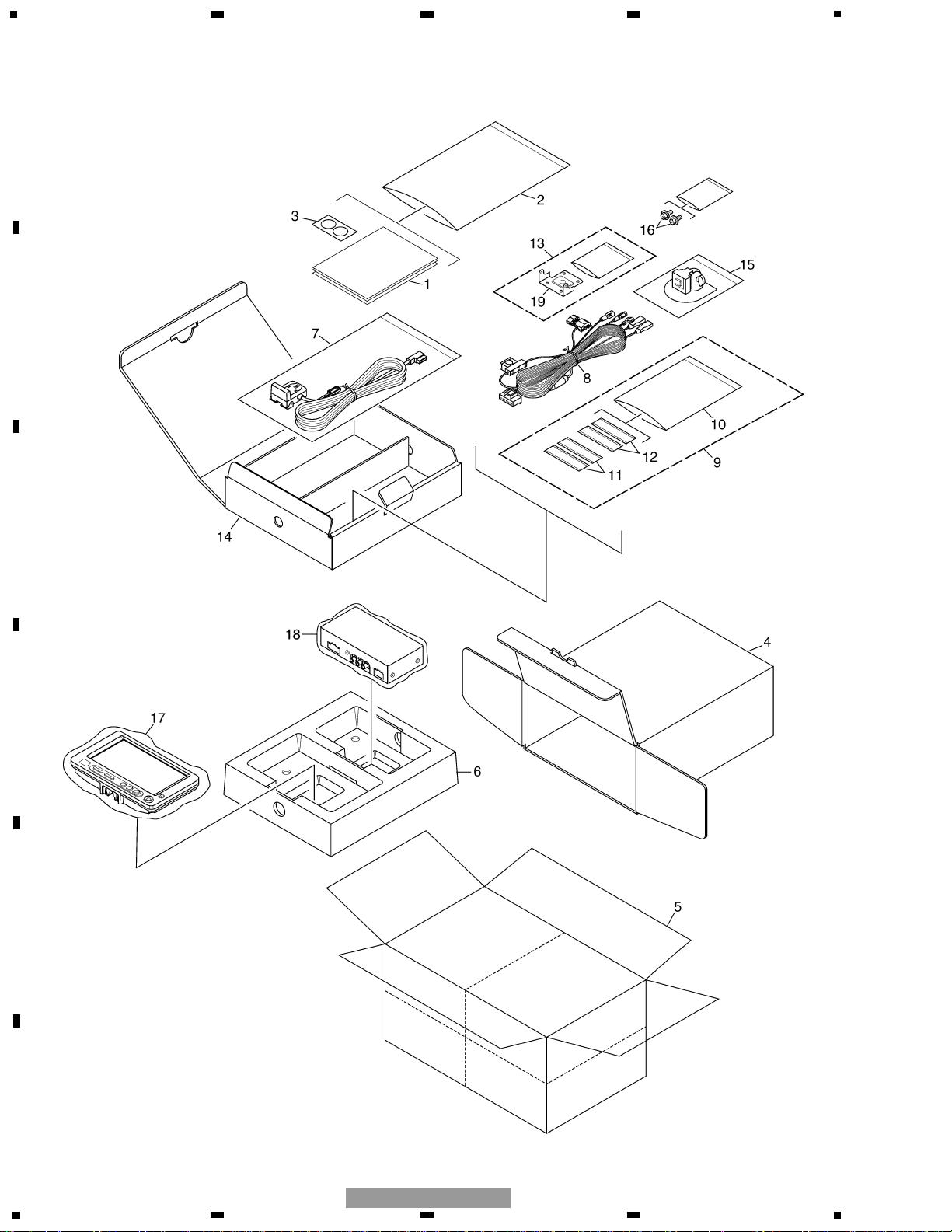
2. EXPLODED VIEWS AND PARTS LIST
2.1 PACKING(AVD-W6210/UC)
Page 7
7
5
6
7
8
F
E
D
C
B
A
5
6
7
8
AVD-W6210/UC
* 1-1 Card ARY1048
1-2 Owner's Manual CRD3800
* 2 Polyethylene Bag CEG1116
3 Cushion CNM4680
4 Carton CHG5104
5 Contain Box CHL5104
6 Protector CHP2724
7 Cord Assy CDE7284
8 Cord Assy CDE7286
9 Accessory Assy CEA2657
* 10 Polyethylene Bag CEG1101
11 Fastener CNM6888
12 Fastener CNM6889
13 Bracket Assy CEA3745
14 Sub Carton CHG5105
15 Monitor Stand Assy CXC1137
16 Screw Assy CZE3078
17 Polyethylene Bag CEG1319
* 18 Polyethylene Bag CEG-186
Mark No. Description Part No.
- PACKING(AVD-W6210/UC) SECTION PARTS LIST
NOTE:
- Parts marked by “*” are generally unavailable because they are not in our Master Spare Parts List.
- Screws adjacent to ∇ mark on the product are used for disassembly.
- For the applying amount of lubricants or glue, follow the instructions in this manual.
(In the case of no amount instructions, apply as you think it appropriate.)
- Owner's Manual
Part No. Language
CRD3800 English, French
Page 8
8
1
234
12
34
F
E
D
C
B
A
AVD-W6210/UC
2.2 PACKING(AVD-W6210/EW)
Page 9
9
5
6
7
8
F
E
D
C
B
A
5
6
7
8
AVD-W6210/UC
- PACKING(AVD-W6210/EW) SECTION PARTS LIST
- Owner's Manual
Part No. Language
CRD3798 English, Spanish, German
CRD3799 French, Italian, Dutch
* 1-1 Warranty Card CRY1157
1-2 Owner's Manual CRD3798
1-3 Owner's Manual CRD3799
* 2 Polyethylene Bag CEG1116
3 Cushion CNM4680
4 Carton CHG5103
5 Contain Box CHL5103
6 Protector CHP2724
7 Detach Assy CXC2019
8 Cord Assy CDE7286
9 Accessory Assy CEA2657
* 10 Polyethylene Bag CEG1101
11 Fastener CNM6888
12 Fastener CNM6889
13 Bracket Assy CEA2823
14 Sub Carton CHG5105
15 Monitor Stand Assy CXB3629
16 Screw HMB40P060FZK
17 Polyethylene Bag CEG1319
* 18 Polyethylene Bag CEG-186
19 Bracket CNC7617
Mark No. Description Part No.
Page 10
10
1
234
12
34
F
E
D
C
B
A
AVD-W6210/UC
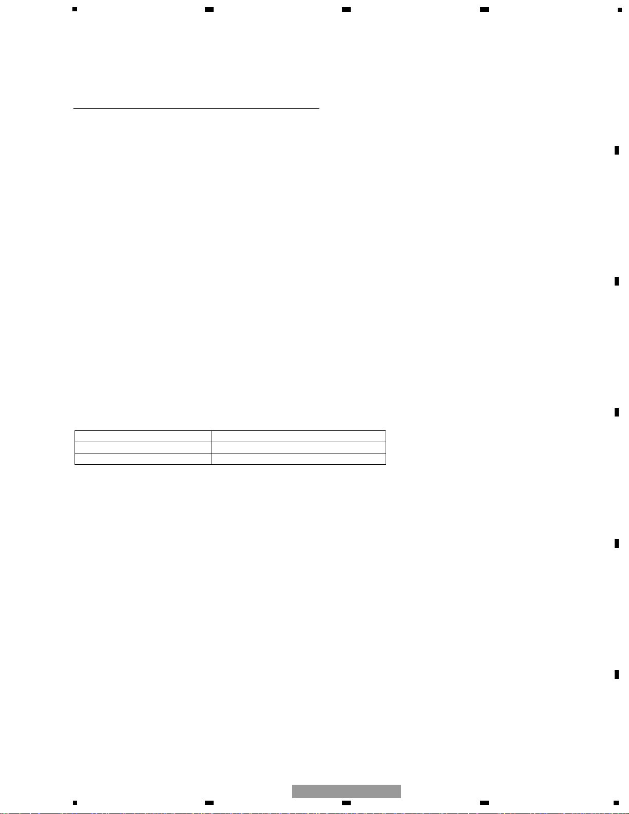
2.3 EXTERIOR(1)(AVD-W6210/UC)
Page 11

11
5
6
7
8
F
E
D
C
B
A
5
6
7
8
AVD-W6210/UC
1 Screw BPZ20P050FTC
2 Screw BPZ20P050FZK
3 Screw BPZ20P080FTC
4 Screw BPZ20P100FZK
5 Holder CNC7283
6 Bracket CNC8398
7 Gasket CNM7413
8 Sheet CNM8339
9 Shield CNM8417
10 Cushion CNM8438
11 Shield CNM8442
12 Case CNS7541
13 Speaker CPV1061
14 Screw CPZ26P100FZK
15 Touch Panel CSX1056
16 LCD Assy CXC1366
17 Screw(M2x2) CBA1551
18 FFC CDE7108
19 Holder CND1315
20 Holder CND1316
21 Insulator CNM8031
22 Sheet CNM8338
23 Insulator CNM8456
24 Monitor Unit CWM8887
25 Terminal(CN4001) CKF1064
26 Terminal(CN4003) CKF1064
27 Terminal(CN4443) CKF1064
28 Connector(CN4202) CKS3124
29 Connector(CN4801) CKS3991
30 Connector(CN4006) CKS4402
31 Connector(CN4442) CKS4428
32 Connector(CN4471) CKS4449
33 Connector(CN4004) CKS4511
34 Connector(CN4201) CKS4647
35 Connector(CN4681) CKS4675
36 Holder CND1317
37 LCD Panel CWX2671
38 Screw IMS20P050FTC
39 Knob Unit CXC1826
40 Grille Unit CXC1827
* 41 Button CAC8117
* 42 Button CAC8118
Mark No. Description Part No.
- EXTERIOR(1)(AVD-W6210/UC) SECTION PARTS LIST
Page 12
12
1
234
12
34
F
E
D
C
B
A
AVD-W6210/UC
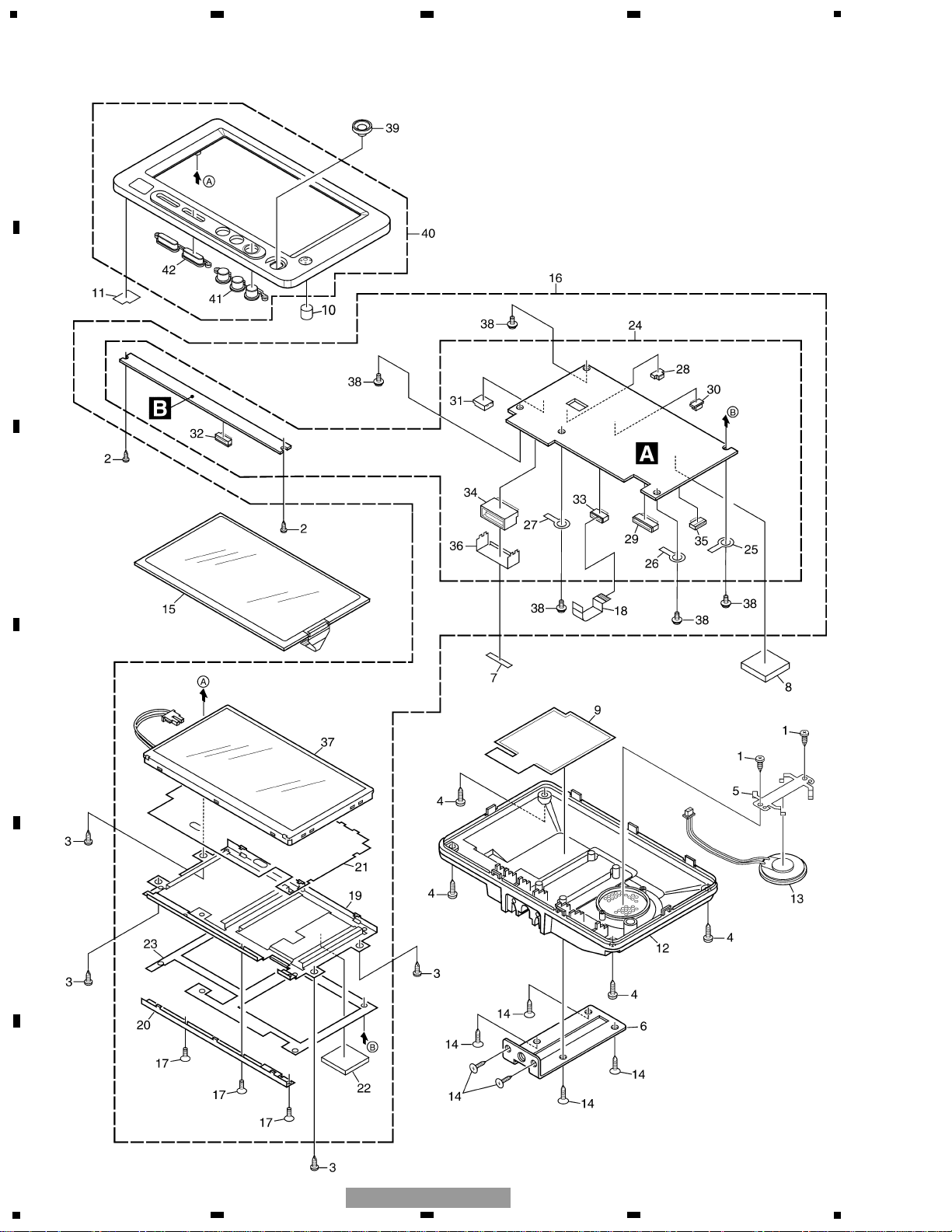
2.4 EXTERIOR(1)(AVD-W6210/EW)
Page 13

13
5
6
7
8
F
E
D
C
B
A
5
6
7
8
AVD-W6210/UC
1 Screw BPZ20P050FTC
2 Screw BPZ20P050FZK
3 Screw BPZ20P080FTC
4 Screw BPZ20P100FZK
5 Holder CNC7283
6 Knob CAC5540
7 Gasket CNM8439
8 Sheet CNM8339
9 Shield CNM8417
10 Cover CNM7159
11 Shield CNM8442
12 Case CNS7557
13 Speaker CPV1061
14 Screw(M2x3) CBA1082
15 Touch Panel CSX1056
16 LCD Assy CXC1264
17 Screw(M2x2) CBA1551
18 FFC CDE7108
19 Holder CND1315
20 Holder CND1316
21 Insulator CNM8031
22 Sheet CNM8338
23 Insulator CNM8456
24 Monitor Unit CWM8852
25 Terminal(CN4001) CKF1064
26 Terminal(CN4003) CKF1064
27 Terminal(CN4443) CKF1064
28 Connector(CN4202) CKS3124
29 Connector(CN4801) CKS3991
30 Connector(CN4006) CKS4402
31 Connector(CN4442) CKS4428
32 Connector(CN4471) CKS4449
33 Connector(CN4004) CKS4511
34 Connector(CN4002) CKS4281
35 Connector(CN4681) CKS4675
36 Holder CND1791
37 LCD Panel CWX2671
38 Screw IMS20P050FTC
39 Knob Unit CXC1826
40 Grille Unit CXC1827
* 41 Button CAC8117
* 42 Button CAC8118
43 Screw(M2x3) CBA1154
44 Spring CBH1708
45 Spring CBH2094
46 Connector CKS3765
47 PCB CNP7278
48 Slider Unit CXB2312
Mark No. Description Part No.
- EXTERIOR(1)(AVD-W6210/EW) SECTION PARTS LIST
Page 14
14
1
234
12
34
F
E
D
C
B
A
AVD-W6210/UC
2.5 EXTERIOR(2)
Page 15
15
5
6
7
8
F
E
D
C
B
A
5
6
7
8
AVD-W6210/UC
1 Screw BSZ30P060FTC
2 Chassis CNA2648
3 Case CNB2867
4 Insulator CNM8281
5 Mother Unit CWM8853
6 Screw BMZ30P060FTC
7 Pin Jack(CN1301) CKB1060
8 Plug(CN1801) CKM1134
9 Jack(CN1201) CKN1032
10 Pin Jack(CN1101) CKS2918
11 •••••
12 Connector(CN1321) CKS4497
13 Connector(CN1841) CKS4647
14 Holder CND1758
15 Cord Assy CDE7286
16 Fuse(4A) CEK1001
17 Cap CNS1472
18 Resistor RS1/2P102JL
19 Holder(B)-L
See Contrast table(2)
20 Holder(B)-R See Contrast table(2)
21 Holder Unit See Contrast table(2)
22 Guide Holder Unit See Contrast table(2)
23 Base Plate Unit See Contrast table(2)
24 Knob Unit See Contrast table(2)
25 Bolt See Contrast table(2)
26 Washer See Contrast table(2)
27 Washer See Contrast table(2)
28 Detach Assy See Contrast table(2)
29 Screw See Contrast table(2)
30 Screw(M2x3) See Contrast table(2)
31 Screw(M2x4.5) See Contrast table(2)
32 Cord Assy See Contrast table(2)
33 Bracket See Contrast table(2)
34 Bracket See Contrast table(2)
35 Case See Contrast table(2)
36 Cover See Contrast table(2)
37 Cover See Contrast table(2)
38 Cover See Contrast table(2)
39 Screw See Contrast table(2)
40 Plug(CN2002) See Contrast table(2)
41 Plug(CN2003) See Contrast table(2)
* 42 Connector(CN2001) See Contrast table(2)
43 Transistor(Q1823,1831) 2SD2375
(1) EXTERIOR(2) SECTION PARTS LIST
Mark No. Description Part No. Mark No. Description Part No.
Part No.
Mark No. Symbol and Description AVD-W6210/UC AVD-W6210/EW
19 Holder(B)-L CZN5455 Not used
20 Holder(B)-R CZN5456 Not used
21 Holder Unit CZX5044 Not used
22 Guide Holder Unit CZX5045 Not used
23 Base Plate Unit CZX5046 Not used
24 Knob Unit CZX5047 Not used
25 Bolt HMZ50Z450FZK Not used
26 Washer WC50FZK Not used
27 Washer WS50FZK Not used
28 Detach Assy Not used CXC2019
29 Screw Not used BPZ26P080FZK
30 Screw(M2x3) Not used CBA1082
31 Screw(M2x4.5) Not used CBA1083
32 Cord Assy Not used CDE7277
33 Bracket Not used CNC7510
34 Bracket Not used CNC7511
35 Case Not used CNS4816
36 Cover Not used CNS4883
37 Cover Not used CNS4884
38 Cover Not used CNV5716
39 Screw Not used CPZ26P080FZK
40 Plug(CN2002) Not used CKS3274
41 Plug(CN2003) Not used CKS3282
* 42 Connector(CN2001) Not used CKS3764
(2) CONTRAST TABLE
AVD-W6210/UC and AVD-W6210/EW are constructed the same except for the following:
Page 16
1
234
12
34
F
E
D
C
B
A
AVD-W6210/UC
16
2
5
7
3
BUP
ACC
PARK
BK
Q1862
IC 1861
PAJ001A
13
9
Q1881
Q1891
57
bksens
58
pbsen
63
asens
62
bsens
5
6
3
S1861
IC 1
PE53
RESET
BU
Q1821
Q1822
BU
65
SYSPW
VSP9
Q1831
VSYSV9
Q1823
VSY5
Q1827
1,2
4
IC 1603
TC7S08FU
9
TXN
12
8
IC 1311
TA2050F
FU1311
10
CN1801
VTR2V
VTR2AL
IC 1
CXA2
9
LV2
8
V2
12
8
IC 1301
TA2050F
FU1301
10
VTR1V
VTR1AL
16
LV3
15
V3
4
3
14
10
13
2
1
13 1IC 1321
TA2050F
2
LV1
CCAUL
CN1301
3
1
IC 1331
NJM4558E
2
ONSEI+
ONSEI-
1
2
IC 1121
TC4S66F
CCSYNC
CCB
CCG
CCR
24
HRXN
25
HTXN
8
RXN
CN1321
C
MOTHER UNIT
NAVIGATION
AV SEL
SYS
CONTR
ISOLATER
ISOLATER
ISOLATER
ISOLATER
18
CCREM
+BATTERY
PARKING BRAKE
REVERSE-GEAR
SIGNAL INPUT
ACC
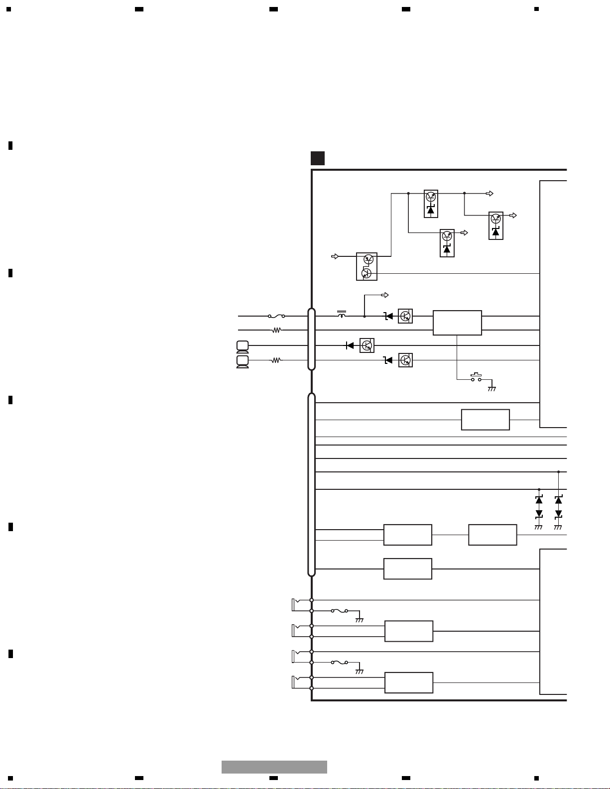
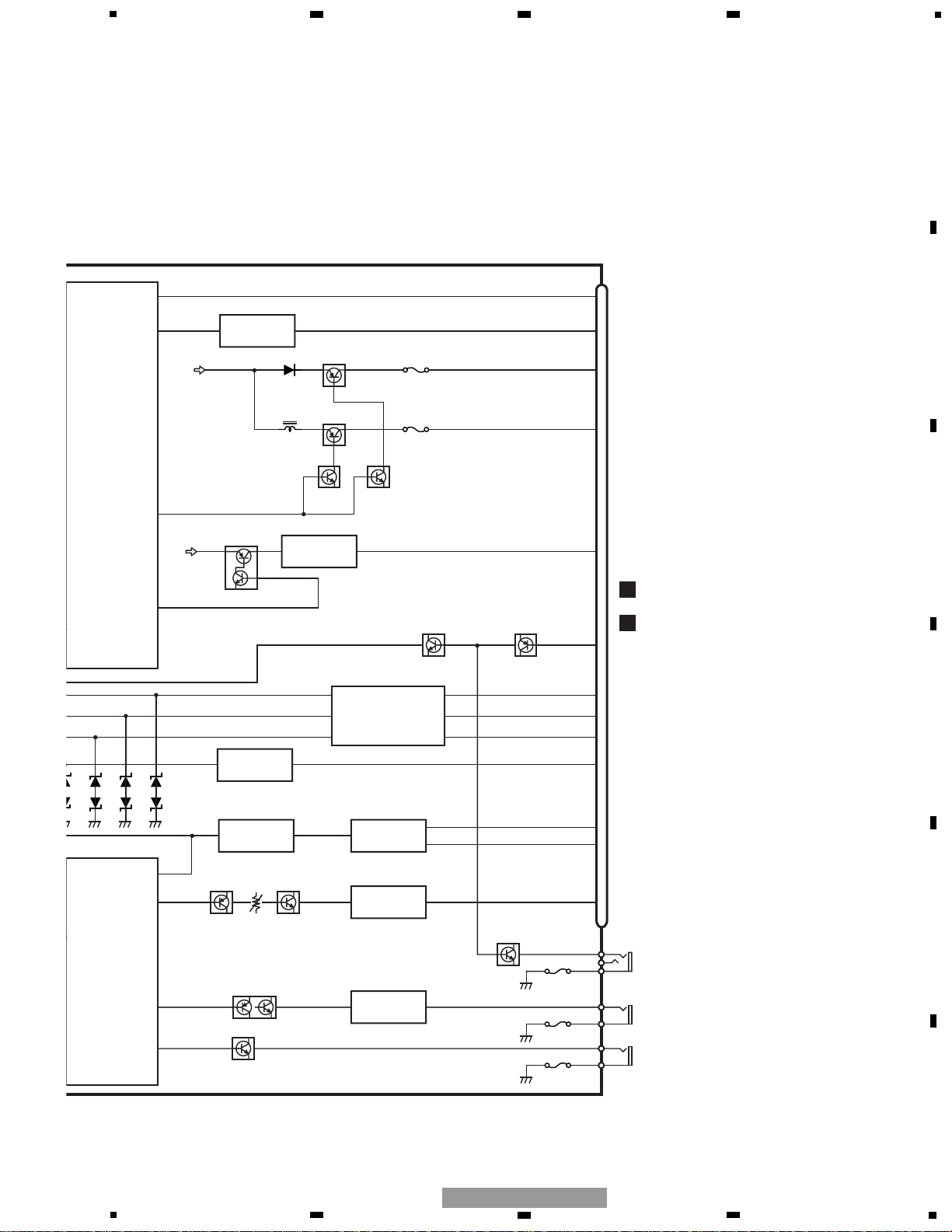
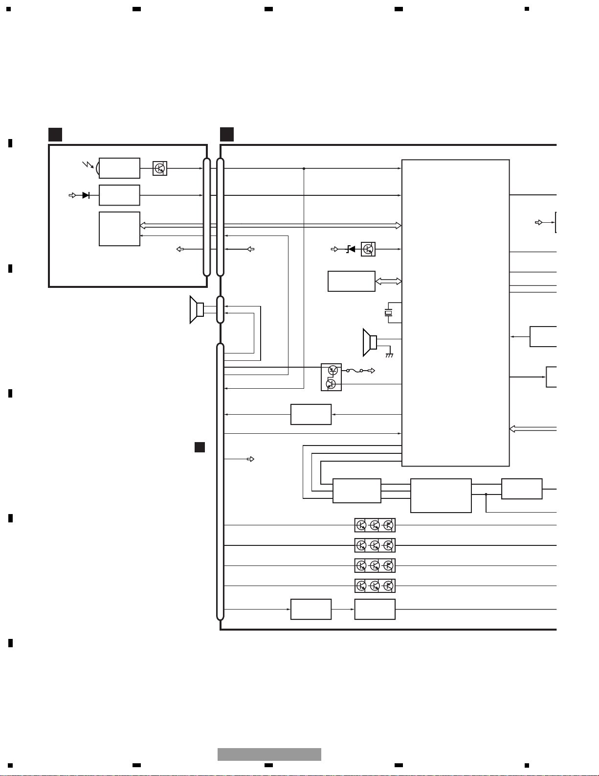
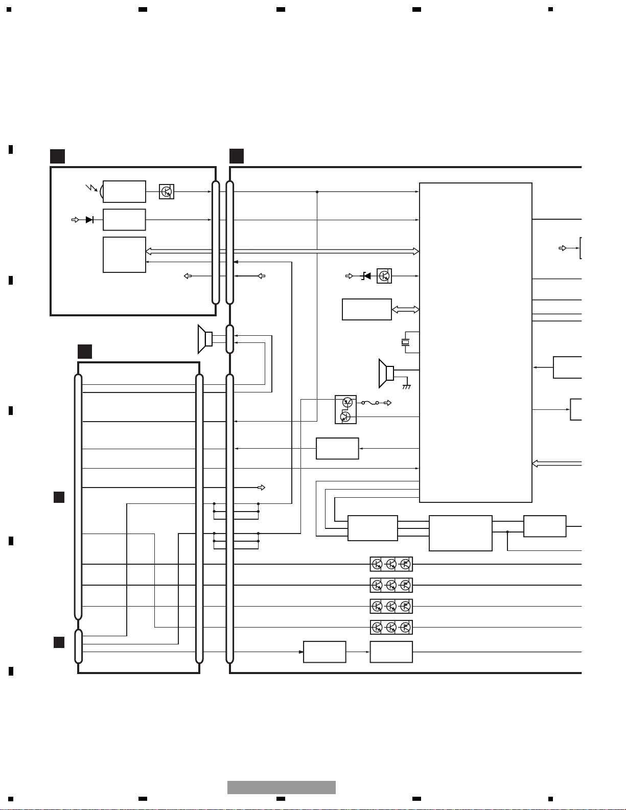
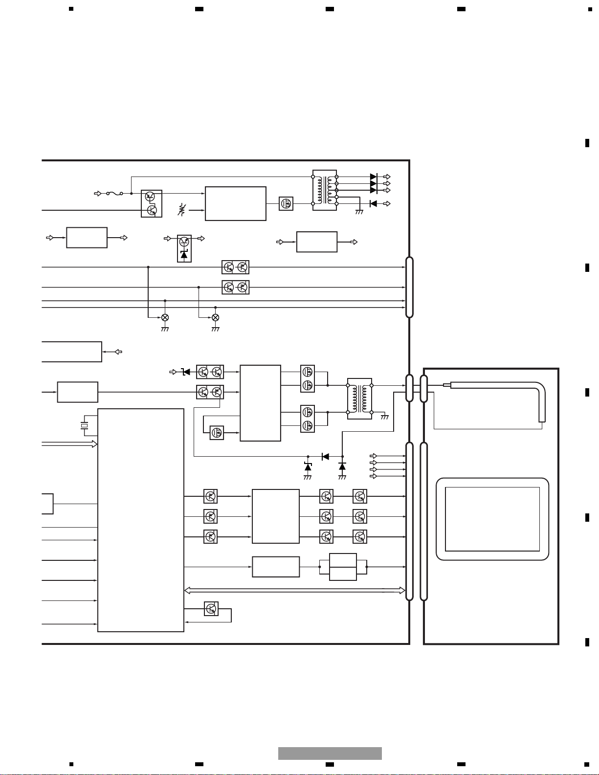
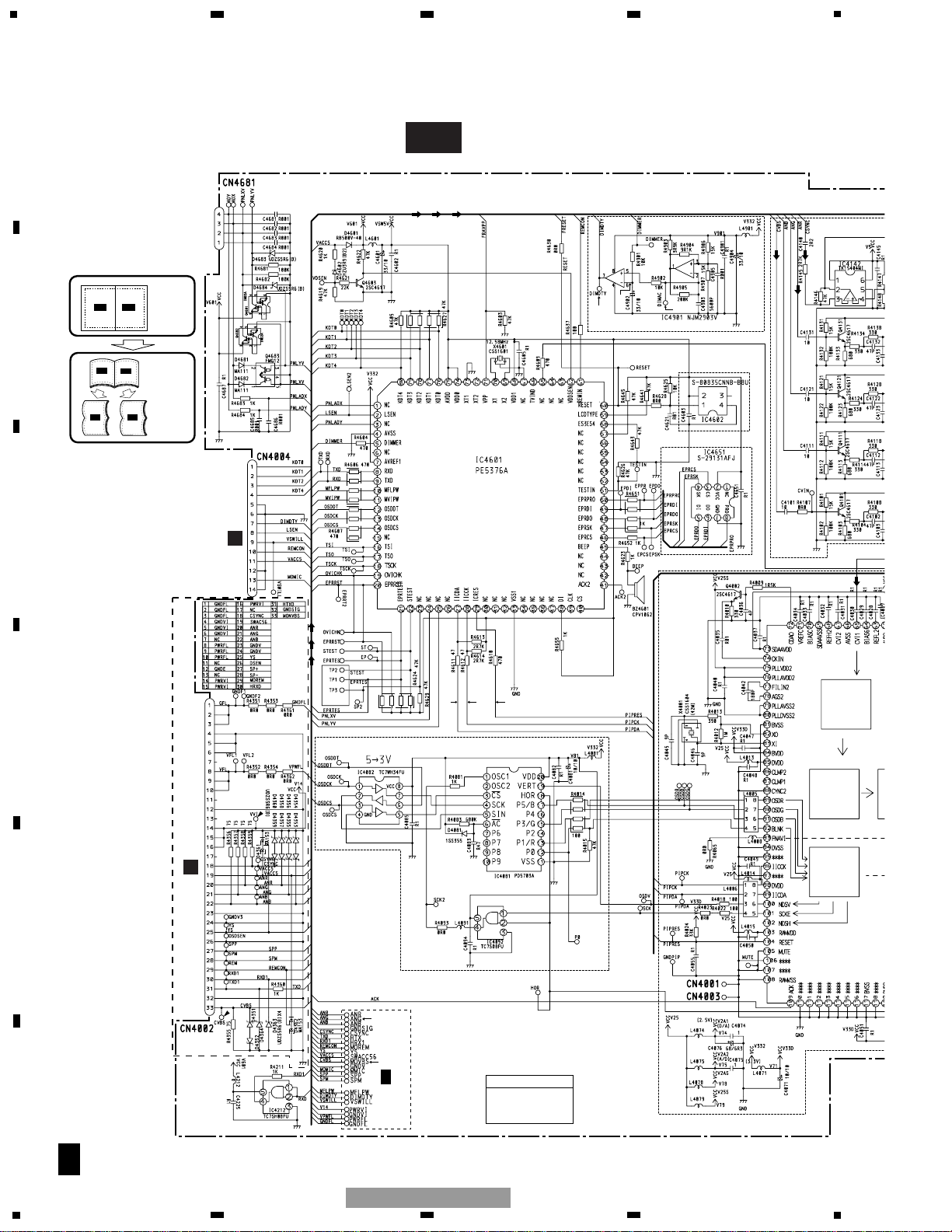
3. BLOCK DIAGRAM AND SCHEMATIC DIAGRAM
3.1 BLOCK DIAGRAM
Page 17
5
6
7
8
F
E
D
C
B
A
5
6
7
8
AVD-W6210/UC
17
bksens
pbsen
asens
bsens
IC 1601
PE5375A
Q1801
Q1802
64
SWACPW
1
3
IC 1801
TA78L05F
BU
SWAC56
SYSPW
1,2 4IC 1602
TC7S08FU
HTXD
12
TXD
HRXD
11
RXD
Q1843
Q1841
BU
FU1841
FU1842
PWRVI
PWRFL
Q1842
Q1844
40
MONPWR
TXN
IC 1271
CXA2069Q
LV2
V2
LV3
V3
LV1
52
LOUT1
2
1
IC 1131
NJM4558E
8
2
IC 1141
TDA7052BT
5
SPP
SPM
4
2
IC 1171
TK15405BMI
CSYNC
IC 1151
BA7660FS
7
2
4
10
15
13
ANR
ANG
ANB
Q1264 Q1262
Q1261
Q1263
VR1261
44
V/YOUT2
53
VOUT1
2
4
IC 1221
TK15405BMI
2
4
IC 1231
TK15405BMI
MONVBS
43
LOUT2
Q1111
RXN
FU1101
FU1102
OUTV
OUTAL
CN1101
6
12
7
26
3
5
23
24
14
25
1
2
CN1841
CN4201(AVD-W6210/UC)
A
CN2003, 2002(AVD-W6210/EW)
D
AV SELECTOR
SYSTEM
CONTROLLER
BUFFER
RGB 75Ω DRIVER
VIDEO DRIVER
VIDEO DRIVER
FU1201
REMOTE
OUT
CN1201
MOREM
8
Q1201
Q1205
Q1202
Page 18
18
1
234
12
34
F
E
D
C
B
A
AVD-W6210/UC
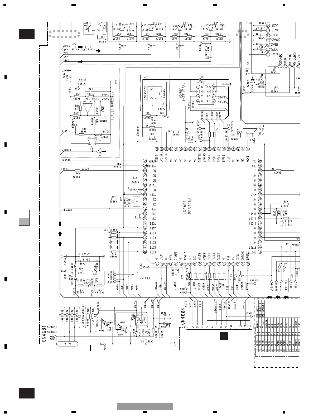
IC 4401
SBX3050-01
87
2
IC 4411
NJM062V
Q4401
AC565
KEY
MATRIX
CN4471
4
SWAC56
6
VSWILL
7
LSENS
5
KREM
11
9
8
10
CN4004
VACC5
VSWILL
LSEN
REMCON
AC565 VACC5
IC4601
PE5376A
REMIN
61
MVIPW
11
LSEN
2
VDDSEN
62
MFLPW
10
RXD
8
TXD
9
KDT0-2,
KDT4
76-78, 80
CN4202
SPP
SPM
1
2
24
CN4201
SPM
23
SPP
12
SWAC56
25
PWRVI
26
PWRFL
6
HTXD
7
HRXD
VACC5
4
1,2
IC 4212
TC7SH08FU
1
ANR
Q4202
Q4201
FL14V
FU4441
VACC5
Q4603
IC 4651
S-29131AFJ
EEPROM
X2
X1
X4601
12.58MHz
69
70
PNLYV
25
PNLADX
1
PNLADY
3
PNLXV
24
DIMMER
5
Q4131-Q4133
2
ANG
Q4121-Q4123
3
ANB
Q4111-Q4113
14
MONVBS
Q4101-Q4103
5
CSYNC
1,2
4
IC 4141
TC7SH08FU
3
2
IC 4142
TK15404MI
6
I
NJ
3
FL14V
X40
42M
8
MOREM
RESET
60
RE
1
IC
S-80835C
CN1841
C
B
A
IC 4082
TC7WH34FU
1
3
6
7
5
2
IC 4081
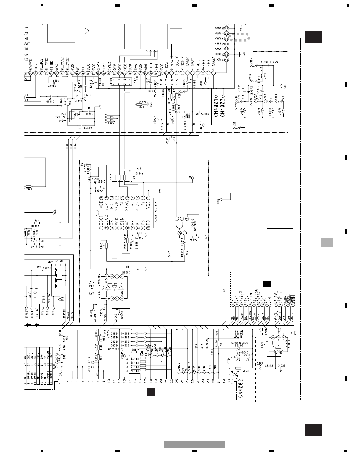
PD5703A
4
3
5
IC 4092
TC7S08FU
1
18
4
2
1
OSDCK
13
OSDCS
14
OSDDT
12
BEEP
45
BZ4601
CPV1062
MONITOR PCBKEYBOARD PCB
SPEAKER
- AVD-W6210/UC
Page 19
19
5
6
7
8
F
E
D
C
B
A
5
6
7
8
AVD-W6210/UC
Q4153(1/2)
Q4152(1/2)
Q4151(1/2)
Q4153(2/2)
Q4152(2/2)
Q4151(2/2)
7
1
RGB AMP
IC 4151
NJM2138V
VCOM AMP
6
2
14
13
Q4156
Q4155
Q4154
52
Q4951
Q4953
T4951
Q4952
VCC
FU4951
IC 4951
FA7700V
VCC
OUT
IN-
7
3
1, 2
4, 5
VR4951
6
6
7
8
9
10
V18
V8
V33
VM12
VFL54
Q4681
CN4681
1
PNLYV
Q4682
3
ADX
4
ADY
2
PNLXV
Q4683 (2/2)
Q4683 (1/2)
IC4001
TC90A64AF-P
RIN
GIN
BIN
CVI1
HDIN
53
54
65
18
CN4801
28
2
VR
VGL
26
VB
17
VCOM
27
VG
ROUT
34
GOUT
36
BOUT
38
POLC
28
Q4182
Q4183
6
1
IC 4181
NJM082BV
VM12
12
VDD3
V33
13
VDD5
V5
15
VGH
V18
Q4002
CDAO
72
CKIN
74
Q4431 Q4432
IC 4441
OZ961IS
2.5V REG.
5V REG.
320
ENA
Q4434 Q4433
7
V2500
4
SST
17
RT
NDRV_B
19
PDRV_A
11
NDRV_D
12
PDRV_C
Q4445
Q4443
Q4444
T4441
2, 3
4, 5
6
7
6
7
IC 4901
NJM2903V
CN4442
1
2
FLP4
FLM4
FL14V
3
1
IC 4442
TA78L05F
V
V25
2
1
IC 4981
R1130H251B
V33
LCD
LCD
BACKLIGHT
V8 V5
Q4991
XO
XI
X4001
42MHz
82
83
VCC
RESET
2
IC 4602
S-80835CNNB-B8U
2
FU
9
CLAMP0
101
SCKE
1
2-screen IC
LCD PANEL
TOUCH PANEL
Page 20
20
1
234
12
34
F
E
D
C
B
A
AVD-W6210/UC
IC 4401
SBX3050-01
87
2
IC 4411
NJM062V
Q4401
AC565
KEY
MATRIX
CN4471
4
SWAC56
6
VSWILL
7
LSENS
5
KREM
11
9
8
10
CN4004
VACC5
VSWILL
LSEN
REMCON
AC565 VACC5
IC4601
PE5376A
REMIN
61
MVIPW
11
LSEN
2
VDDSEN
62
MFLPW
10
RXD
8
TXD
9
KDT0-2,
KDT4
76-78, 80
CN4202
SPP
SPM
1
2
28
CN4002
SPM
27
SPP
19
SWAC56
14
PWRVI
8
PWRFL
31
HTXD
30
HRXD
VACC5
4
1,2
IC 4212
TC7SH08FU
20
ANR
Q4202
Q4201
FL14V
FU4441
VACC5
Q4603
IC 4651
S-29131AFJ
EEPROM
X2
X1
X4601
12.58MHz
69
70
PNLYV
25
PNLADX
1
PNLADY
3
PNLXV
24
DIMMER
5
Q4131-Q4133
21
ANG
Q4121-Q4123
22
ANB
Q4111-Q4113
33
MONVBS
Q4101-Q4103
18
CSYNC
1,2
4
IC 4141
TC7SH08FU
3
2
IC 4142
TK15404MI
6
I
NJ
3
FL14V
X40
42M
29
MOREM
RESET
60
RE
1
IC 4
S-80835C
CN1841
C
B
A
IC 4082
TC7WH34FU
1
3
6
7
5
2
IC 4081
PD5703A
4
3
5
IC 4092
TC7S08FU
1
18
4
2
1
OSDCK
13
OSDCS
14
OSDDT
12
BEEP
45
BZ4601
CPV1062
MONITOR PCBKEYBOARD PCB
SPEAKER
15
PWRVI
16
PWRVI
9
PWRFL
10
PWRFL
15
14
7
5
3
18
17
8
9
10
20
6
16
6
CSYNC
3
PWRFL
1
PWRVI
9
8
1
14
12
11
2
3
4
10
SPM
SPP
MOREM
HRXD
HTXD
VSWAC5
MONVBS
ANR
ANG
ANB
D
DETACH UNIT
CN2001CN2003
CN2002
CN1841
C
- AVD-W6210/EW
Page 21
21
5
6
7
8
F
E
D
C
B
A
5
6
7
8
AVD-W6210/UC
Q4153(1/2)
Q4152(1/2)
Q4151(1/2)
Q4153(2/2)
Q4152(2/2)
Q4151(2/2)
7
1
RGB AMP
IC 4151
NJM2138V
VCOM AMP
6
2
14
13
Q4156
Q4155
Q4154
52
Q4951
Q4953
T4951
Q4952
VCC
FU4951
IC 4951
FA7700V
VCC
OUT
IN-
7
3
1, 2
4, 5
VR4951
6
6
7
8
9
10
V18
V8
V33
VM12
VFL54
Q4681
CN4681
1
PNLYV
Q4682
3
ADX
4
ADY
2
PNLXV
Q4683 (2/2)
Q4683 (1/2)
IC4001
TC90A64AF-P
RIN
GIN
BIN
CVI1
HDIN
53
54
65
18
CN4801
28
2
VR
VGL
26
VB
17
VCOM
27
VG
ROUT
34
GOUT
36
BOUT
38
POLC
28
Q4182
Q4183
6
1
IC 4181
NJM082BV
VM12
12
VDD3
V33
13
VDD5
V5
15
VGH
V18
Q4002
CDAO
72
CKIN
74
Q4431 Q4432
IC 4441
OZ961IS
2.5V REG.
5V REG.
320
ENA
Q4434 Q4433
7
V2500
4
SST
17
RT
NDRV_B
19
PDRV_A
11
NDRV_D
12
PDRV_C
Q4445
Q4443
Q4444
T4441
2, 3
4, 5
6
7
6
7
IC 4901
NJM2903V
CN4442
1
2
FLP4
FLM4
FL14V
3
1
IC 4442
TA78L05F
V25
2
1
IC 4981
R1130H251B
V33
LCD
LCD
BACKLIGHT
V8 V5
Q4991
XO
XI
X4001
42MHz
82
83
VCC
RESET
2
IC 4602
9
CLAMP0
101
SCKE
1
2-screen IC
LCD PANEL
TOUCH PANEL
Page 22
1
234
12
34
F
E
D
C
B
A
AVD-W6210/UC
22
A-a A-b
A-a
A-b
A-b
A-a
Large size
SCH diagram
Guide page
Detailed page
Note: When ordering service parts, be sure to refer to " EXPLODED VIEWS AND PARTS LIST" or
"ELECTRICAL PARTS LIST".
A-a
1/2
A
1/2
AVD-W6210/EW ONLY
Y/C SEPARAT
A/D 8bit
OSD
INTERFACE
DIMMER
RESET
EEPROM
FILTER
OSD CONTROL
2/2
A
D
CN2001
TOUCH PANEL
B
CN4471
R
V
S
V RS
S
V
R
V
$
0
&*(
9
8
7
%
MONITOR UNIT
Consists of
MONITOR PCB
KEYBOARD PCB
3.2 MONITOR PCB (PICTURE PROCESSING)(GUIDE PAGE)
Page 23
5
6
7
8
F
E
D
C
B
A
5
6
7
8
AVD-W6210/UC
23
A-b
1/2
A
1/2
Y/C SEPARAT
A/D 8bit
A/D 8bit
NTSC Dec
IMAGE
PROCESSING
RGB
OverLayCont
2M DRAM
D/A 10bit
MULTI
SCREEN
PROCESSING
P in P
OSD
INTERFACE
TFT
CONTROLLER
FILTER
RGB AMP
VCOM AMP
2-screen IC
LCD PANEL
Decimal points for resistor
and capacitor fixed values
are expressed as :
2.2 2R2
0.022 R022
←
←
The > mark found on some component parts indicates
the importance of the safety factor of the part.
Therefore, when replacing, be sure to use parts of
identical designation.
Symbol indicates a resistor.
No differentiation is made between chip resistors and
discrete resistors.
NOTE :
Symbol indicates a capacitor.
No differentiation is made between chip capacitors and
discrete capacitors.
: The power supply is shown with the marked box.
1/2
A
MONITOR PCB (PICTURE PROCESSING)
>
R
V
S
: SYNC SIGNAL
: VIDEO SIGNAL
: RED SIGNAL
S
R
R
V
V
S
S
R
R
R
R
%
!
@
)
›
⁄
fi
¤
‹
#
^
1 2
6
3
4
5
V25 : 2.5V
V33 : 3.3V
V5 : 5.0V
V8 : 8.0V
V18 : 18V
VM12 : -12V
Page 24
1
234
12
34
F
E
D
C
B
A
AVD-W6210/UC
24
A-a
A-a
(1/2)
A-b
1/2
A-a
1/2
A-b
(1/2)
2
1
AVD-W6210/EW ONLY
DIMMER
RESET
EEPROM
FILTER
TOUCH PANEL
B
CN4471
R
V
S
V RS
S
V
R
V
9
8
7
Page 25
5
6
7
8
F
E
D
C
B
A
5
6
7
8
AVD-W6210/UC
25
A-a
A-b
1/2
A-a
1/2
A-a
(1/2)
A-b
(1/2)
3
Y/C SEPARAT
A/D 8bi
OSD
INTERFACE
OSD CONTROL
2/2
A
D
CN2001
V
S
$
0
&*(
MONITOR UNIT
Consists of
MONITOR PCB
KEYBOARD PCB
Page 26
1
234
12
34
F
E
D
C
B
A
AVD-W6210/UC
26
A-b
1/2
A-a
(1/2)
A-b
(1/2)
2
1
FILTER
RGB AMP
2-screen IC
1/2
A
MONITOR PCB (PICTURE PROCESSING)
>
R
V
S
: SYNC SIGNAL
: VIDEO SIGNAL
: RED SIGNAL
S
R
R
V
V
S
R
R
%
!
@
‹
#
^
1 2
6
3
4
5
V25 : 2.5V
V33 : 3.3V
V5 : 5.0V
V8 : 8.0V
V18 : 18V
VM12 : -12V
Page 27
5
6
7
8
F
E
D
C
B
A
5
6
7
8
AVD-W6210/UC
27
A-b
1/2
A-a
(1/2)
A-b
(1/2)
3
A/D 8bit
A/D 8bit
NTSC Dec
IMAGE
PROCESSING
RGB
OverLayCont
2M DRAM
D/A 10bit
MULTI
SCREEN
PROCESSING
P in P
OSD
TFT
CONTROLLER
VCOM AMP
LCD PANEL
Decimal points for resistor
and capacitor fixed values
are expressed as :
2.2 2R2
0.022 R022
←
←
The > mark found on some component parts indicates
the importance of the safety factor of the part.
Therefore, when replacing, be sure to use parts of
identical designation.
Symbol indicates a resistor.
No differentiation is made between chip resistors and
discrete resistors.
NOTE :
Symbol indicates a capacitor.
No differentiation is made between chip capacitors and
discrete capacitors.
: The power supply is shown with the marked box.
S
R
R
R
R
)
›
⁄
fi
¤
‹
Page 28

28
1
234
12
34
F
E
D
C
B
A
AVD-W6210/UC
2/2
A
AVD-W6210/UC ONLY
AVD-W6210/EW ONLY
1/2
A
>
SPEAKER
C
CN1841
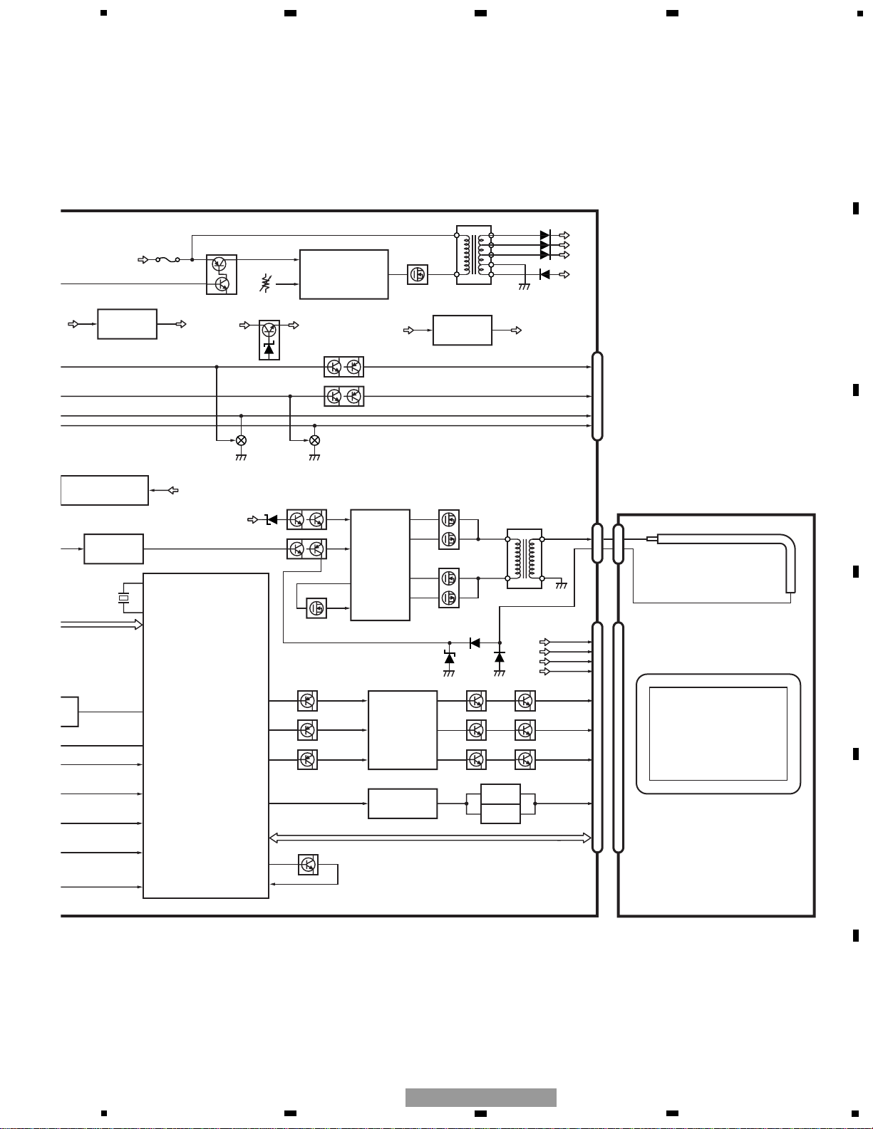
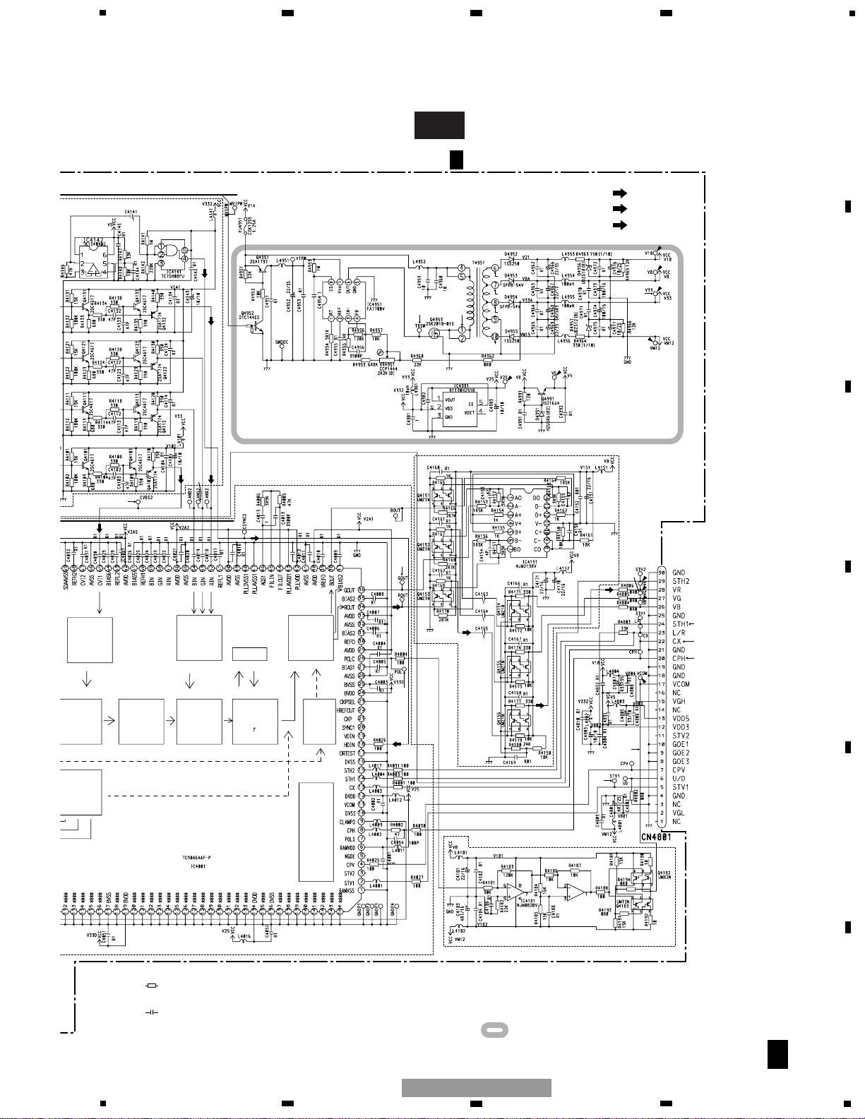
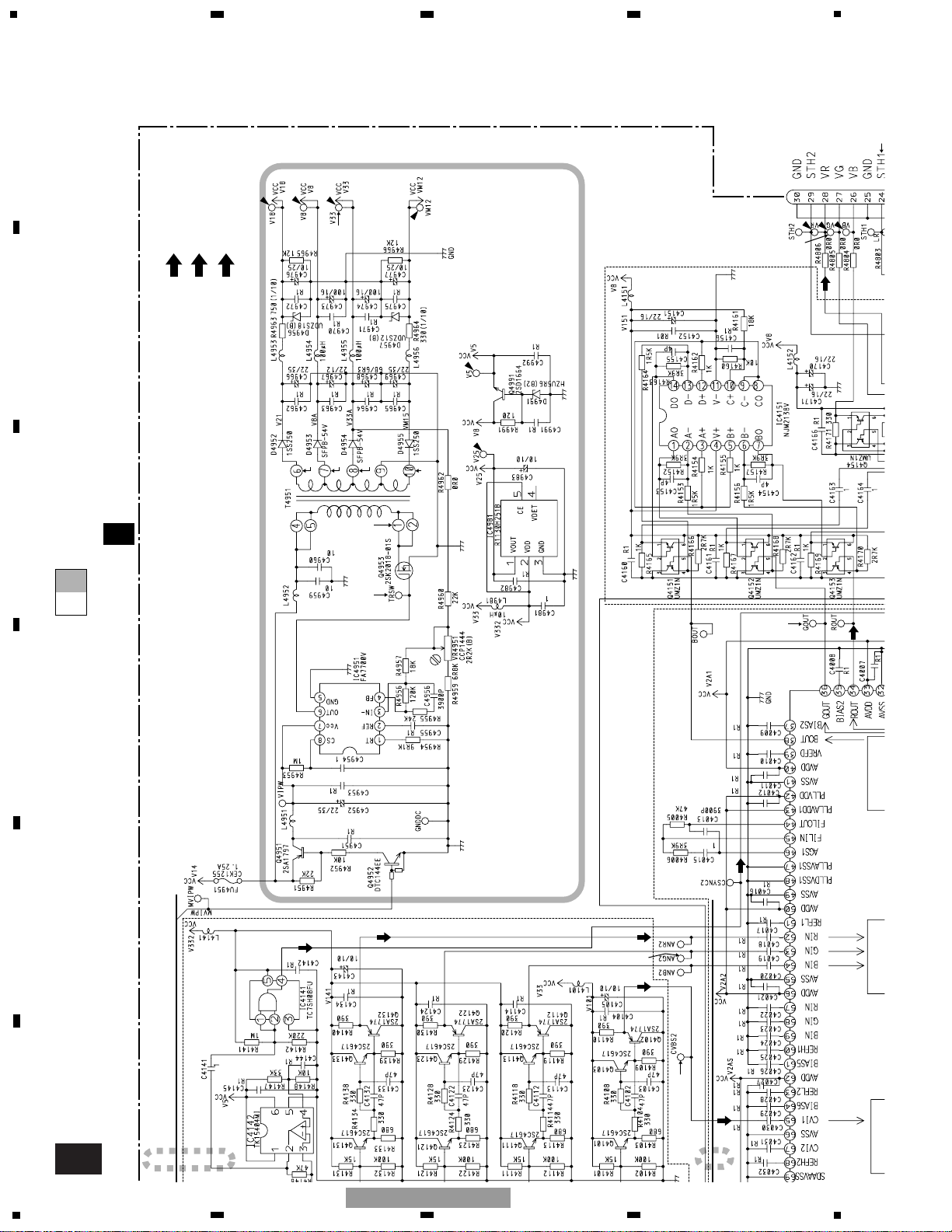
3.3 MONITOR PCB (INVERTER)
Page 29

29
5
6
7
8
F
E
D
C
B
A
5
6
7
8
AVD-W6210/UC
2/2
A
2/2
A
1/2
A
MONITOR PCB (INVERTER)
LCD
PANEL
MONITOR UNIT
Consists of
MONITOR PCB
KEYBOARD PCB
Page 30

1
234
12
34
F
E
D
C
B
A
AVD-W6210/UC
30
- Waveforms Note : The encircled numbers denote measuring pointes in circuit diagram.
CH1 : 1 TRSW CH2 : 2 T4951 Pin 1
CH1 : 3 T4951 Pin 6
CH3 : 5 T4951 Pin 8
CH2 : 4 T4951 Pin 7
CH4 : 6 T4951 Pin 10
CH1 : 7 IC4901 Pin 2
CH3 : 9 IC4901 Pin 7
CH2 : 8 IC4901 Pin 6
CH1 : Color bar G signal
CH3 : ! ANG2
CH2 : 0 ANG
CH1 : Color bar G signal
CH3 : @ GOUT
CH2 : 0 ANG
CH4 : # VG
CH1 : 10 STEP VTR IN
CH3 : % CVBS2
CH2 : $ CVBS
Page 31

5
6
7
8
F
E
D
C
B
A
5
6
7
8
AVD-W6210/UC
31
CH1 : 10 STEP VTR IN
CH3 : @ GOUT
CH2 : $ CVBS
CH4 : # VG
CH1 : ^ V33
CH3 : * PIPCK
CH2 : & PIPRES
CH4 : ( PIPDA
CH1 : 10 STEP VTR IN
CH3 : ⁄ VCOM
CH2 : ) POL
CH4 : # VG
CH1 : 10 STEP VTR IN
CH3 : ‹ STH1
CH2 : ¤ CX
CH4 : # VG
CH1 : ^ V33
CH3 : * PIPCK
CH2 : & PIPRES
CH4 : ( PIPDA
CH1 : 10 STEP VTR IN
CH3 : › STV1
CH2 : ¤ CX
CH4 : # VG
Page 32

1
234
12
34
F
E
D
C
B
A
AVD-W6210/UC
32
CH1 : 10 STEP VTR IN
CH3 : # VG
CH2 : fi CPH
Page 33

5
6
7
8
F
E
D
C
B
A
5
6
7
8
AVD-W6210/UC
33
B
B
KEYBOARD PCB
CN4004
SOURCE/POWER
WIDE
NAVI/AV
NAVI
NAVI MENU
ADJUST
VOLUME-
VOLUME+
MONITOR UNIT
Consists of
MONITOR PCB
KEYBOARD PCB
1/2
A
1
6
4
3
5
8
7
2
3.4 KEYBOARD PCB
Page 34

1
234
12
34
F
E
D
C
B
A
AVD-W6210/UC
34
C-a
C
V2 AUDIO ISOLATOR
V1 AUDIO ISOLATOR
NAVIGATION RGB INPUT
SOURCE SELECTOR
POWER SUPPLY
SYSTEM SECTION
MONITOR SECTION
AUDIO SECTION
BACK UP AND REMOTE CONTROL POWER SUPPLY
SENSOR
NAVIGAT
MONITOR ON
PARKING ON/OFF
BACK
AUDIO O
SOURCE SE
1
2
3
4
5
6
7
8
9
10
11
12
NAVIGATION
VTR IN 1VTR IN 2
REMOTE OUT
>
>
>
>
>
>
R
V
S
A
: AUDIO SIGNAL
: SYNC SIGNAL
: VIDEO SIGNAL
: RED SIGNAL
R
S
S
R
V
A
V
A
A
V
V
A
V
A
A
3.5 MOTHER UNIT(GUIDE PAGE)
Page 35

5
6
7
8
F
E
D
C
B
A
5
6
7
8
AVD-W6210/UC
35
C-b
C
DETACH
NAVIGATION
MONITOR ON
ON/OFF
RGB 75Ω DRIVER
REMOTE CONTROL BUFFER
BUFFER
MICRO COMPUTER
75Ω VIDEO DRIVER
AUDIO OUTPUT BUFFER MUTE
SOURCE SELECTOR BUFFER
MONITOR SPEAKER AUDIO OUTPUT
MONITOR SPEAKER ATTENUATION AND MUTE
1
2
3
4
5
6
VTR OUT
>
>
2/2
A
CN4201 (AVD-W6210/UC)
D
CN2003, 2002 (AVD-W6210/EW)
C
MOTHER UNIT
V
V
A
A
A
A
RR
S
S
A
RS
A
A
A
V
V
V
V
A
1
2
Page 36

36
1
234
12
34
F
E
D
C
B
A
AVD-W6210/UC
A-a
C-a
C-b
C-a
C-b
1
2
NAVIGATION RGB INPUT
SOURCE SELECTOR
POWER SUPPLY
SYSTEM SECTION
AUDIO SECTION
NAVIGATION
REMOTE OUT
>
>
R
V
S
A
: AUDIO SIGNAL
: SYNC SIGNAL
: VIDEO SIGNAL
: RED SIGNAL
R
S
S
R
V
A
V
A
A
V
V
A
V
Page 37

37
5
6
7
8
F
E
D
C
B
A
5
6
7
8
AVD-W6210/UC
A-a
C-b
C-a
C-a
C-b
5
43
V2 AUDIO ISOLATOR
V1 AUDIO ISOLATOR
SYSTEM SECTION
MONITOR SECTION
BACK UP AND REMOTE CONTROL POWER SUPPLY
SENSOR
PARKING ON/OFF
BACK
12345
6
789
101112
VTR IN 1VTR IN 2
>
>
>
>
>
V
A
A
Page 38

38
1
234
12
34
F
E
D
C
B
A
AVD-W6210/UC
C-b
C-a
C-b
1
2
RGB 75Ω DRIVER
REMOTE CONTROL BUFFER
BUFFER
MICRO COMPUTER
75Ω VIDEO DRIVER
AUDIO OUTPUT BUFFER MUTE
SOURCE SELECTOR BUFFER
MONITOR SPEAKER AUDIO OUTPUT
MONITOR SPEAKER ATTENUATION AND MUTE
2/2
A
CN4201 (AVD-W6210/UC)
D
CN2003, 2002 (AVD-W6210/EW)
C
MOTHER UNIT
A
V
V
A
V
V
A
A
A
A
RR
S
S
A
RS
A
A
V
A
Page 39

39
5
6
7
8
F
E
D
C
B
A
5
6
7
8
AVD-W6210/UC
C-b
C-a
C-b
5
43
DETACH
NAVIGATION
MONITOR ON
75Ω VIDEO DRIVER
12345
6
VTR OUT
>
>
>
>
2/2
A
CN
D
CN20
A
V
V
V
V
A
1
2
Page 40

40
1
234
12
34
F
E
D
C
B
A
AVD-W6210/UC
- Waveforms Note : The encircled numbers denote measuring pointes in circuit diagram.
INPUT : Color bar signal
CH1 : 1 MONVBS CH2 : 2 REOUT
Page 41

41
5
6
7
8
F
E
D
C
B
A
5
6
7
8
AVD-W6210/UC
D
D
DETACH UNIT
C
CN1841
1/2
A
CN4002
3.6 DETACH UNIT(AVD-W6210/EW)
Page 42

42
1
234
12
34
F
E
D
C
B
A
AVD-W6210/UC
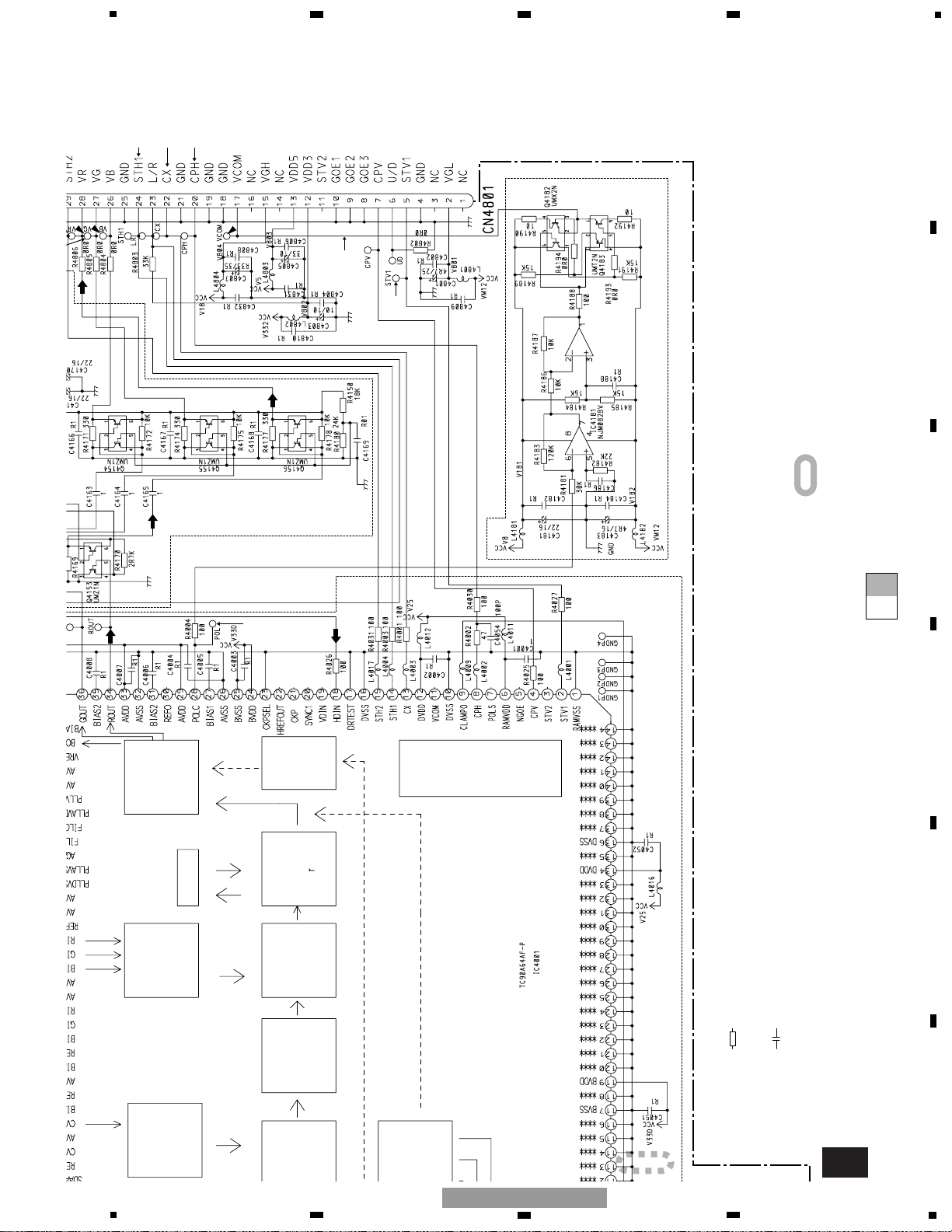
4. PCB CONNECTION DIAGRAM
4.1 MONITOR PCB
Capacitor
Connector
P.C.Board
Chip Part
A
A
MONITOR PCB
SIDE B
SIDE A
NOTE FOR PCB DIAGRAMS
1.The parts mounted on this PCB
include all necessary parts for
several destination.
For further information for
respective destinations, be sure
to check with the schematic dia gram.
2.Viewpoint of PCB diagrams
B
C
TOUCH PANEL
LCD PANEL
Page 43

43
5
6
7
8
F
E
D
C
B
A
5
6
7
8
AVD-W6210/UC
A
SIDE A
D
CN2001
B
CN4471
C
CN1841
SPEAKER
(AVD-W6210/EW)
(AVD-W6210
/UC)
LCD PANEL
Page 44

44
1
234
12
34
F
E
D
C
B
A
AVD-W6210/UC
A
A
MONITOR PCB
Page 45

45
5
6
7
8
F
E
D
C
B
A
5
6
7
8
AVD-W6210/UC
A
SIDE B
Page 46

46
1
234
12
34
F
E
D
C
B
A
AVD-W6210/UC
C
C
MOTHER UNIT
FRO
A
CN4201 (AVD-W6210/UC)
NAVIGATION
D
CN2003, 2002 (AVD-W6210/EW)
VTR OUT
REMOTE OUT
5
6
4
3
4.2 MOTHER UNIT
Page 47

47
5
6
7
8
F
E
D
C
B
A
5
6
7
8
AVD-W6210/UC
C
SIDE A
FRONT
CORD ASSY
RESET
VTR IN
4
3
2
1
612
11
5
39
10
4
17
8
2
Page 48

48
1
234
12
34
F
E
D
C
B
A
AVD-W6210/UC
C
C
MOTHER UNIT
TP1823
TP1827
1
1
Page 49

49
5
6
7
8
F
E
D
C
B
A
5
6
7
8
AVD-W6210/UC
C
SIDE B
SPVOL
MONVBS
Page 50

50
1
234
12
34
F
E
D
C
B
A
AVD-W6210/UC
B
B
KEYBOARD PCB
B
KEYBOARD PCB
SIDE A
SIDE B
A
CN4004
SOURCE/POWER WIDE VOLUME- VOLUME+
NAVI/AV NAVI NAVI MENU ADJUST
4.3 KEYBOARD PCB
Page 51

51
5
6
7
8
F
E
D
C
B
A
5
6
7
8
AVD-W6210/UC
D
D
DETACH UNIT
D
DETACH UNIT
SIDE A
SIDE B
A
CN4002
C
CN1841
C
CN1841
4.4 DETACH UNIT(AVD-W6210/EW)
Page 52

52
1
234
12
34
F
E
D
C
B
A
AVD-W6210/UC
Unit Number : CWM8853
Unit Name : Mother Unit
MISCELLANEOUS
IC 1121 IC TC4S66F
IC 1131 IC NJM4558E
IC 1141 IC TDA7052BT
IC 1151 IC BA7660FS
IC 1171 IC TK15405BMI
IC 1221 IC TK15405BMI
IC 1231 IC TK15405BMI
IC 1271 IC CXA2069Q
IC 1301 IC TA2050F
IC 1311 IC TA2050F
IC 1321 IC TA2050F
IC 1331 IC NJM4558E
IC 1601 IC PE5375A
IC 1602 IC TC7S08FU
IC 1603 IC TC7S08FU
IC 1801 IC TA78L05F
IC 1861 IC PAJ001A
Q 1111 Transistor 2SC4081
Q 1112 Transistor 2SC4081
Q 1113 Transistor FMG12
Q 1121 Transistor FMG12
Q 1122 Transistor FMG12
Q 1123 Transistor DTC144EU
Q 1141 Transistor DTC114EU
Q 1201 Transistor 2SA1576
Q 1202 Transistor 2SC4081
Q 1203 Transistor DTC144EU
Q 1204 Transistor 2SC4081
Q 1205 Transistor 2SC4081
Q 1261 Transistor 2SC4081
Q 1262 Transistor 2SC4081
Q 1263 Transistor 2SA1576
Q 1264 Transistor 2SA1576
Q 1601 Transistor DTA144EU
Q 1602 Transistor DTA144EU
Q 1604 Transistor DTA144EU
Q 1605 Transistor DTA144EU
Q 1606 Transistor DTA144EU
Q 1801 Transistor 2SA1036K
Q 1802 Transistor 2SC4081
Q 1821 Transistor 2SA1615-Z
Q 1822 Transistor DTC114EU
Q 1823 Transistor 2SD2375
Q 1827 Transistor 2SD1664
Q 1831 Transistor 2SD2375
Q 1832 Transistor 2SC4081
Q 1841 Transistor 2SA1615-Z
Q 1842 Transistor DTC114EU
Q 1843 Transistor 2SA1615-Z
Q 1844 Transistor DTC114EU
Q 1862 Transistor DTC114EU
Q 1881 Transistor 2SC4081
Q 1891 Transistor 2SA1576
Q 1892 Transistor 2SC4081
Q 1893 Transistor 2SC4081
Q 1901 Transistor 2SC4081
D 1111 Diode MA152WA
D 1121 Diode MA152WA
D 1122 Diode MA152WA
D 1141 Diode UDZS10(B)
D 1142 Diode UDZS10(B)
D 1151 Diode MA153
D 1152 Diode MA153
D 1153 Diode MA153
D 1171 Diode MA153
D 1181 Diode UDZS8R2(B)
D 1201 Diode 1SS355
D 1202 Diode 1SS355
D 1203 Diode 1SS355
D 1204 Diode 1SS355
D 1221 Diode MA153
D 1231 Diode MA153
D 1251 Diode UDZS5R6(B)
D 1252 Diode UDZS5R6(B)
D 1253 Diode UDZS5R6(B)
D 1254 Diode UDZS5R6(B)
D 1255 Diode UDZS5R6(B)
D 1256 Diode UDZS5R6(B)
D 1257 Diode HZU2R0(B)
D 1258 Diode HZU2R0(B)
D 1271 Diode HZU2R0(B)
D 1272 Diode HZU2R0(B)
D 1275 Diode HZU2R0(B)
D 1276 Diode HZU2R0(B)
D 1277 Diode HZU2R0(B)
D 1278 Diode HZU2R0(B)
D 1301 Diode UDZS5R6(B)
D 1302 Diode UDZS5R6(B)
D 1303 Diode UDZS5R6(B)
D 1304 Diode UDZS5R6(B)
D 1311 Diode UDZS5R6(B)
D 1312 Diode UDZS5R6(B)
D 1313 Diode UDZS5R6(B)
D 1314 Diode UDZS5R6(B)
D 1321 Diode UDZS5R6(B)
D 1322 Diode UDZS5R6(B)
D 1323 Diode UDZS5R6(B)
D 1324 Diode UDZS5R6(B)
D 1601 Diode MA153
D 1602 Diode MA153
D 1604 Diode MA153
D 1605 Diode MA153
D 1802 Diode 1SS355
D 1803 Diode 5KP24A
D 1823 Diode UDZS9R1(B)
5. ELECTRICAL PARTS LIST
NOTES:
- Parts whose parts numbers are omitted are subject to being not supplied.
- The part numbers shown below indicate chip components.
Chip Resistor
RS1/_S___J,RS1/__S___J
Chip Capacitor (except for CQS.....)
CKS....., CCS....., CSZS.....
=====Circuit Symbol and No.===Part Name Part No.
--- ------ ------------------------------------------ -------------------------
=====Circuit Symbol and No.===Part Name Part No.
--- ------ ------------------------------------------ -------------------------
C
Page 53

53
5
6
7
8
F
E
D
C
B
A
5
6
7
8
AVD-W6210/UC
D 1827 Diode UDZS5R6(B)
D 1831 Diode UDZS10(B)
D 1842 Diode SC016-2
D 1861 Diode SC016-2
D 1862 Diode UDZS18(B)
D 1863 Diode 1SS355
D 1881 Diode UDZS6R8(B)
D 1891 Diode MA152WK
D 1892 Diode 1SS355
L 1141 Inductor LCKB4R7M2520
L 1151 Inductor LCKA150J2520
L 1171 Inductor LCTC120K2125
L 1221 Inductor LCTC120K2125
L 1231 Inductor LCTC120K2125
L 1261 Inductor LCTC4R7K1608
L 1262 Inductor LCTC4R7K1608
L 1271 Inductor LCKA100J2520
L 1601 Inductor LCKA150J2520
L 1602 Inductor LCKA150J2520
L 1801 Choke Coil 2.4mH CTH1101
L 1823 Inductor LCKB150K2520
L 1824 Inductor LCKB150K2520
L 1841 Choke Coil 100µH CTH1140
L 1842 Inductor CTH1256
L 1881 Inductor CTF1295
L 1891 Inductor CTF1295
X 1601 Radiator 12.58MHz CSS1601
S 1861 Switch(RESET) CSG1020
VR 1261 Semi-fixed 4.7kΩ(B) CCP1446
FU 1101 Fuse 2A CEK1257
FU 1102 Fuse 2A CEK1257
FU 1201 Fuse 2A CEK1257
FU 1301 Fuse 2A CEK1257
FU 1311 Fuse 2A CEK1257
FU 1321 Fuse 2A CEK1257
FU 1841 Fuse 1.6A CEK1256
FU 1842 Fuse 2A CEK1257
RESISTORS
R 1101 RS1/16S182J
R 1102 RS1/16S182J
R 1111 RS1/16S471J
R 1112 RS1/16S471J
R 1113 RS1/16S821J
R 1114 RS1/16S821J
R 1115 RS1/16S104J
R 1116 RS1/16S104J
R 1117 RS1/16S821J
R 1118 RS1/16S821J
R 1121 RS1/16S153J
R 1122 RS1/16S153J
R 1123 RS1/16S223J
R 1124 RS1/16S223J
R 1125 RS1/16S104J
R 1126 RS1/16S104J
R 1127 RS1/16S392J
R 1128 RS1/16S392J
R 1129 RS1/16S473J
R 1130 RS1/16S822J
R 1131 RS1/16S223J
R 1132 RS1/16S223J
R 1133 RS1/16S0R0J
R 1134 RS1/16S103J
R 1135 RS1/16S102J
R 1141 RS1/16S562J
R 1142 RS1/16S223J
R 1144 RS1/16S103J
R 1152 RS1/16S684J
R 1153 RS1/16S104J
R 1154 RS1/16S684J
R 1155 RS1/16S104J
R 1156 RS1/16S684J
R 1157 RS1/16S104J
R 1158 RS1/16S750J
R 1159 RS1/16S750J
R 1160 RS1/16S750J
R 1172 RS1/16S750J
R 1201 RS1/16S223J
R 1202 RS1/16S473J
R 1203 RS1/16S473J
R 1204 RS1/16S473J
R 1205 RS1/16S472J
R 1207 RS1/16S473J
R 1208 RS1/16S102J
R 1209 RS1/16S473J
R 1210 RS1/16S103J
R 1211 RS1/16S102J
R 1212 RS1/16S472J
R 1213 RS1/16S471J
R 1222 RS1/16S750J
R 1232 RS1/16S750J
R 1251 RS1/16S750J
R 1252 RS1/16S750J
R 1253 RS1/16S750J
R 1254 RS1/16S750J
R 1261 RS1/16S223J
R 1262 RS1/16S471J
R 1263 RS1/16S103J
R 1264 RS1/16S471J
R 1265 RS1/16S103J
R 1266 RS1/16S183J
R 1267 RS1/16S102J
R 1268 RS1/16S102J
R 1273 RS1/16S562J
R 1274 RS1/16S562J
R 1277 RS1/16S562J
R 1278 RS1/16S562J
R 1279 RS1/16S562J
R 1280 RS1/16S562J
R 1281 RS1/16S101J
R 1282 RS1/16S101J
R 1283 RS1/16S470J
R 1284 RS1/16S470J
R 1285 RS1/16S750J
R 1286 RS1/16S750J
R 1287 RS1/16S0R0J
R 1288 RS1/16S750J
R 1289 RS1/16S473J
R 1301 RS1/16S101J
R 1302 RS1/16S101J
R 1303 RS1/16S223J
R 1304 RS1/16S223J
R 1305 RS1/16S102J
R 1306 RS1/16S102J
R 1311 RS1/16S101J
R 1312 RS1/16S101J
R 1313 RS1/16S223J
R 1314 RS1/16S223J
R 1315 RS1/16S102J
=====Circuit Symbol and No.===Part Name Part No.
--- ------ ------------------------------------------ -------------------------
=====Circuit Symbol and No.===Part Name Part No.
--- ------ ------------------------------------------ -------------------------
Page 54

R 1316 RS1/16S102J
R 1321 RS1/16S101J
R 1322 RS1/16S101J
R 1323 RS1/16S223J
R 1324 RS1/16S223J
R 1325 RS1/16S102J
R 1326 RS1/16S102J
R 1331 RS1/16S473J
R 1332 RS1/16S473J
R 1333 RS1/16S102J
R 1334 RS1/16S103J
R 1335 RS1/16S103J
R 1336 RS1/16S473J
R 1337 RS1/16S473J
R 1602 RS1/16S681J
R 1603 RS1/16S681J
R 1611 RS1/16S103J
R 1616 RS1/16S681J
R 1617 RS1/16S681J
R 1618 RS1/16S681J
R 1619 RS1/16S681J
R 1621 RS1/16S681J
R 1628 RAB4CQ681J
R 1629 RAB4CQ681J
R 1630 RAB4CQ681J
R 1641 RS1/16S681J
R 1642 RS1/16S681J
R 1643 RS1/16S681J
R 1644 RS1/16S681J
R 1645 RS1/16S103J
R 1646 RS1/16S470J
R 1647 RS1/16S103J
R 1648 RS1/16S470J
R 1651 RS1/16S681J
R 1652 RS1/16S681J
R 1653 RS1/16S681J
R 1654 RS1/16S681J
R 1655 RS1/16S473J
R 1656 RS1/16S473J
R 1657 RS1/16S473J
R 1659 RS1/16S473J
R 1660 RS1/16S473J
R 1661 RS1/16S473J
R 1662 RS1/16S473J
R 1691 RS1/16S473J
R 1801 RS1/16S0R0J
R 1802 RS1/16S562J
R 1803 RS1/16S153J
R 1804 RS1/16S473J
R 1805 RS1/16S473J
R 1806 RS1/10S0R0J
R 1821 RS1/16S153J
R 1822 RS1/4S301J
R 1823 RS1/4S301J
R 1824 RS1/16S681J
R 1827 RS1/16S681J
R 1831 RS1/10S681J
R 1832 RS1/16S684J
R 1841 RS1/16S153J
R 1842 RS1/4S301J
R 1843 RS1/4S301J
R 1844 RS1/16S153J
R 1845 RS1/4S152J
R 1864 RS1/16S223J
R 1865 RS1/16S103J
R 1866 RS1/16S104J
R 1867 RS1/16S104J
R 1868 RS1/16S104J
R 1869 RN1/16SE1001D
R 1870 RS1/16S101J
R 1871 RS1/16S104J
R 1872 RS1/16S563J
R 1873 RS1/16S393J
R 1874 RS1/16S623J
R 1875 RS1/16S134J
R 1881 RS1/10S103J
R 1882 RS1/16S103J
R 1883 RS1/16S103J
R 1884 RS1/16S473J
R 1890 RS1/16S473J
R 1891 RS1/16S473J
R 1892 RS1/16S223J
R 1893 RS1/16S473J
R 1894 RS1/16S473J
R 1895 RS1/16S473J
R 1896 RS1/16S473J
R 1897 RS1/16S473J
R 1898 RS1/16S473J
R 1899 RS1/16S473J
R 1900 RS1/16S473J
R 1901 RS1/16S473J
R 1902 RS1/16S473J
R 1903 RS1/16S473J
CAPACITORS
C 1101 CKSRYB222K50
C 1102 CKSRYB222K50
C 1103 CKSRYB104K16
C 1111 CEV100M16
C 1112 CEV100M16
C 1113 CKSRYB222K50
C 1114 CKSRYB222K50
C 1121 CKSRYB105K10
C 1122 CKSRYB105K10
C 1123 CEV101M16
C 1124 CKSRYB104K16
C 1125 CKSRYB105K10
C 1126 CKSRYB105K10
C 1131 CKSRYB105K10
C 1132 CCSRCH821J50
C 1133 CKSRYB105K10
C 1134 CKSRYB104K16
C 1141 CKSRYB104K16
C 1142 CKSRYB474K10
C 1143 CKSRYB104K16
C 1145 100µF/16V CCH1228
C 1147 CCSRCH101J50
C 1148 CCSRCH101J50
C 1151 CKSRYB105K10
C 1152 CKSRYB105K10
C 1153 CKSRYB105K10
C 1154 CEV101M16
C 1155 CKSRYB103K50
C 1156 CEV101M16
C 1157 CEV220M16
C 1158 CEV101M16
C 1159 CEV220M16
C 1160 CEV101M16
C 1161 CEV220M16
C 1171 CKSQYB225K10
54
1
234
12
34
F
E
D
C
B
A
AVD-W6210/UC
=====Circuit Symbol and No.===Part Name Part No.
--- ------ ------------------------------------------ -------------------------
=====Circuit Symbol and No.===Part Name Part No.
--- ------ ------------------------------------------ ------------------------C 1172 CKSYB106K6R3
Page 55

C 1173 CKSRYB103K50
C 1175 CEV101M16
C 1176 CEV220M16
C 1201 CKSRYB103K50
C 1221 CKSYB475K16
C 1222 CEV330M10
C 1223 CEV330M10
C 1225 CEV330M10
C 1226 CKSRYB103K50
C 1231 CKSYB475K16
C 1232 CEV330M10
C 1233 CEV330M10
C 1235 CEV330M10
C 1236 CKSRYB103K50
C 1261 CCSRCH5R0D50
C 1262 CCSRCH5R0D50
C 1263 CKSRYB103K50
C 1264 CKSRYB103K50
C 1274 CKSRYB474K10
C 1275 CKSRYB105K10
C 1276 CKSRYB105K10
C 1280 CKSRYB474K10
C 1281 CKSRYB105K10
C 1282 CKSRYB105K10
C 1283 CKSRYB105K10
C 1284 CKSRYB474K10
C 1285 CKSRYB105K10
C 1286 CKSRYB103K50
C 1287 CEV220M16
C 1288 CEV100M16
C 1301 CKSRYB105K10
C 1302 CKSRYB105K10
C 1303 CKSRYB105K10
C 1304 CKSRYB105K10
C 1305 CEV220M16
C 1306 CEV100M16
C 1307 CCSRCH471J50
C 1308 CCSRCH471J50
C 1311 CKSRYB105K10
C 1312 CKSRYB105K10
C 1313 CKSRYB105K10
C 1314 CKSRYB105K10
C 1315 CEV220M16
C 1316 CEV100M16
C 1317 CCSRCH471J50
C 1318 CCSRCH471J50
C 1321 CKSRYB105K10
C 1322 CKSRYB105K10
C 1323 CKSRYB105K10
C 1324 CKSRYB105K10
C 1325 CEV220M16
C 1326 CEV100M16
C 1327 CCSRCH471J50
C 1328 CCSRCH471J50
C 1331 CKSRYB105K10
C 1332 CKSRYB105K10
C 1333 CKSRYB104K16
C 1334 CKSRYB105K10
C 1601 CKSRYB104K16
C 1602 CEV101M16
C 1603 CKSRYB104K16
C 1604 CKSRYB104K16
C 1605 CKSRYB105K10
C 1607 CKSRYB104K16
C 1608 CKSRYB104K16
C 1665 CKSRYB103K50
C 1801
CEHAT102M16(P35)
C 1802 CKSRYF104Z25
C 1803 CKSRYF104Z25
C 1804 CKSRYF104Z25
C 1805 100µF/16V CCH1228
C 1806 CKSRYB103K50
C 1821 100µF/16V CCH1228
C 1822 CKSRYB103K50
C 1823 100µF/16V CCH1228
C 1824 CKSRYB103K50
C 1825 CKSRYB103K50
C 1826 100µF/16V CCH1228
C 1827 100µF/16V CCH1228
C 1828 CKSRYB103K50
C 1829 CKSRYB103K50
C 1830 100µF/16V CCH1228
C 1831 CEV101M16
C 1832 CKSRYB103K50
C 1833 100µF/16V CCH1228
C 1834 CKSRYB103K50
C 1835 CEV101M16
C 1836 CKSRYB103K50
C 1837 CEV101M16
C 1838 CKSRYB103K50
C 1839 CKSRYB473K50
C 1840 CEV101M16
C 1841 CEV101M16
C 1842 CKSRYF104Z25
C 1843
CEHAT102M16(P35)
C 1844 CKSRYF104Z25
C 1845 CEV101M16
C 1846 CKSRYF104Z25
C 1847 100µF/16V CCH1228
C 1848 CKSRYF104Z25
C 1849 CKSRYB473K50
C 1861 CKSRYB103K50
C 1863 CEV100M16
C 1864 CEV101M16
C 1869 CKSRYF104Z25
C 1871 CKSRYB104K16
C 1872 CEHAT222M16
C 1873 CKSRYB103K50
C 1874 CKSRYB103K50
C 1882 CKSRYF104Z25
C 1891 CKSRYF103Z50
C 1892 CKSRYF103Z50
Unit Number : CWM8887(AVD-W6210/UC)
CWM8852(AVD-W6210/EW)
Unit Name : Monitor Unit
MISCELLANEOUS
IC 4001 IC TC90A64AF-P
IC 4081 IC PD5703A
IC 4082 IC TC7WH34FU
IC 4092 IC TC7S08FU
IC 4141 IC TC7SH08FU
IC 4142 IC TK15404MI
IC 4151 IC NJM2138V
IC 4181 IC NJM082BV
IC 4212 IC TC7SH08FU
IC 4401 IC SBX3050-01
55
5
6
7
8
F
E
D
C
B
A
5
6
7
8
AVD-W6210/UC
=====Circuit Symbol and No.===Part Name Part No.
--- ------ ------------------------------------------ -------------------------
=====Circuit Symbol and No.===Part Name Part No.
--- ------ ------------------------------------------ -------------------------
A
B
Monitor Unit
Consists of
Monitor PCB
Keyboard PCB
Page 56

IC 4411 IC NJM062V
IC 4441 IC OZ961IS
IC 4442 IC TA78L05F
IC 4601 IC PE5376A
IC 4602 IC
S-80835CNNB-B8U
IC 4651 IC S-29131AFJ
IC 4901 IC NJM2903V
IC 4951 IC FA7700V
IC 4981 IC R1130H251B
Q 4002 Transistor 2SC4617
Q 4101 Transistor 2SC4617
Q 4102 Transistor 2SA1774
Q 4103 Transistor 2SC4617
Q 4111 Transistor 2SC4617
Q 4112 Transistor 2SA1774
Q 4113 Transistor 2SC4617
Q 4121 Transistor 2SC4617
Q 4122 Transistor 2SA1774
Q 4123 Transistor 2SC4617
Q 4131 Transistor 2SC4617
Q 4132 Transistor 2SA1774
Q 4133 Transistor 2SC4617
Q 4151 Transistor UMZ1N
Q 4152 Transistor UMZ1N
Q 4153 Transistor UMZ1N
Q 4154 Transistor UMZ1N
Q 4155 Transistor UMZ1N
Q 4156 Transistor UMZ1N
Q 4182 Transistor UMX2N
Q 4183 Transistor UMT2N
Q 4201 Transistor DTC144EU
Q 4202 Transistor 2SA1615-Z
Q 4401 Transistor DTC144TE
Q 4431 Transistor 2SC4617
Q 4432 Transistor 2SC4617
Q 4433 Transistor DTA144EU
Q 4434 Transistor 2SC4081
Q 4443 FET SI6544DQ
Q 4444 FET SI6544DQ
Q 4445 FET 2SK1062
Q 4603 Transistor 2SC4617
Q 4681 Transistor IMD2A
Q 4682 Transistor IMD2A
Q 4683 Transistor FMG12
Q 4951 Transistor 2SA1797
Q 4952 Transistor DTC144EE
Q 4953 Transistor 2SK2018-01S
Q 4991 Transistor 2SD1664
D 4081 Diode 1SS355
D 4201 Diode (AVD-W6210/UC) MA153
D 4202 Diode (AVD-W6210/UC) MA153
D 4203 Diode (AVD-W6210/UC) MA153
D 4204 Diode (AVD-W6210/UC) UDZS5R6(B)
D 4205 Diode (AVD-W6210/UC) UDZS5R6(B)
D 4206 Diode (AVD-W6210/UC) UDZS5R6(B)
D 4207 Diode (AVD-W6210/UC) UDZS5R6(B)
D 4208 Diode (AVD-W6210/UC) UDZS5R6(B)
D 4209 Diode (AVD-W6210/UC) UDZS5R6(B)
D 4210 Diode (AVD-W6210/UC) UDZS5R6(B)
D 4211 Diode (AVD-W6210/UC) UDZS5R6(B)
D 4212 Diode (AVD-W6210/UC) UDZS5R6(B)
D 4213 Diode (AVD-W6210/UC) UDZS5R6(B)
D 4214 Diode (AVD-W6210/UC) UDZS5R6(B)
D 4215 Diode (AVD-W6210/UC) UDZS5R6(B)
D 4351 Diode (AVD-W6210/EW) UDZS5R6(B)
D 4352 Diode (AVD-W6210/EW) UDZS5R6(B)
D 4353 Diode (AVD-W6210/EW) UDZS5R6(B)
D 4354 Diode (AVD-W6210/EW) UDZS5R6(B)
D 4355 Diode (AVD-W6210/EW) UDZS5R6(B)
D 4356 Diode (AVD-W6210/EW) UDZS5R6(B)
D 4357 Diode (AVD-W6210/EW) UDZS5R6(B)
D 4358 Diode (AVD-W6210/EW) UDZS5R6(B)
D 4359 Diode (AVD-W6210/EW) UDZS5R6(B)
D 4360 Diode (AVD-W6210/EW) UDZS5R6(B)
D 4361 Diode (AVD-W6210/EW) MA153
D 4362 Diode (AVD-W6210/EW) MA153
D 4363 Diode (AVD-W6210/EW) UDZS5R6(B)
D 4364 Diode (AVD-W6210/EW) UDZS5R6(B)
D 4411 Photodiode AM-30-21
D 4412 Diode RB500V-40
D 4431 Diode UDZS6R2(B)
D 4440 Diode HZU6R2(B3)
D 4441 Diode HZU6R2(B3)
D 4442 Diode HZU6R2(B3)
D 4443 Diode MA143
D 4444 Diode MA143
D 4473 LED CL-195PG-CD
D 4474 LED CL-195PG-CD
D 4475 LED CL-195PG-CD
D 4476 LED CL-195PG-CD
D 4477 LED CL-195PG-CD
D 4481 Diode UDZS5R6(B)
D 4482 Diode UDZS5R6(B)
D 4483 Diode UDZS5R6(B)
D 4484 Diode UDZS5R6(B)
D 4485 Diode UDZS5R6(B)
D 4486 Diode UDZS5R6(B)
D 4487 Diode UDZS5R6(B)
D 4488 Diode UDZS5R6(B)
D 4601 Diode RB500V-40
D 4602 Diode HZU3R9(B2)
D 4681 Diode MA111
D 4682 Diode MA111
D 4683 Diode UDZS5R6(B)
D 4684 Diode UDZS5R6(B)
D 4952 Diode 1SS250
D 4953 Diode SFPB-54V
D 4954 Diode SFPB-54V
D 4955 Diode 1SS250
D 4956 Diode UDZS18(B)
D 4957 Diode UDZS12(B)
D 4991 Diode HZU5R6(B2)
L 4001 Inductor CTF1306
L 4002 Inductor CTF1306
L 4003 Inductor CTF1306
L 4004 Inductor CTF1306
L 4005 Inductor-Array CTF1421
L 4006 Inductor-Array CTF1421
L 4008 Inductor CTF1306
L 4009 Ferrite Beed CTF1528
L 4011 Inductor CTF1306
L 4012 Ferrite Beed CTF1528
L 4013 Ferrite Beed CTF1528
L 4014 Ferrite Beed CTF1528
L 4015 Inductor CTF1306
L 4016 Ferrite Beed CTF1528
L 4017 Inductor CTF1306
L 4071 Inductor LCTA100J2520
L 4074 Inductor LCTA100J2520
L 4075 Inductor LCTA100J2520
56
1
234
12
34
F
E
D
C
B
A
AVD-W6210/UC
=====Circuit Symbol and No.===Part Name Part No.
--- ------ ------------------------------------------ -------------------------
=====Circuit Symbol and No.===Part Name Part No.
--- ------ ------------------------------------------ -------------------------
Page 57

L 4078 Inductor LCTA100J2520
L 4079 Inductor CTF1306
L 4081 Inductor LCTA101J2520
L 4091 Inductor CTF1306
L 4101 Inductor LCTA100J2520
L 4141 Inductor LCTA100J2520
L 4151 Inductor LCTA100J2520
L 4152 Inductor LCTA100J2520
L 4181 Inductor LCTA101J2520
L 4182 Inductor LCTA101J2520
L 4201 Inductor CTH1256
L 4212 Inductor CTF1388
L 4411 Inductor LCTA150J2520
L 4441 Inductor CTH1262
L 4601 Inductor LCTA100J2520
L 4801 Inductor LCTA100J2520
L 4802 Inductor LCTA100J2520
L 4803 Inductor LCTA100J2520
L 4804 Inductor LCTA100J2520
L 4901 Inductor LCTA2R2J2520
L 4951 Inductor LCTA100J2520
L 4952 Coil CTH1195
L 4953 Inductor LCTA100J2520
L 4954 Choke Coil 100µH CTH1302
L 4955 Choke Coil 100µH CTH1302
L 4956 Inductor LCTA100J2520
L 4981 Choke Coil 10µH CTH1249
T 4441 Transformer CTT1103
T 4951 Transformer CTT1110
X 4001 Crystal Resonator 42.000MHz CSS1604
X 4601 Radiator 12.58MHz CSS1601
S 4471 Push Switch CSG1112
S 4472 Push Switch CSG1112
S 4473 Push Switch CSG1111
S 4474 Push Switch CSG1111
S 4475 Push Switch CSG1111
S 4476 Push Switch CSG1112
S 4477 Push Switch CSG1112
S 4478 Switch CSX1047
VR 4951 Semi-fixed 2.2Ω(B) CCP1444
FU 4441 Fuse 1.25A CEK1255
FU 4951 Fuse 1.25A CEK1255
BZ 4601 Buzzer CPV1062
RESISTORS
R 4001 RS1/16S101J
R 4002 RS1/16S470J
R 4003 RS1/16S101J
R 4004 RS1/16S101J
R 4005 RS1/16S473J
R 4006 RS1/16S392J
R 4009 RS1/16S152J
R 4010 RS1/16S331J
R 4012 RS1/16SS105J
R 4013 RS1/16S391J
R 4014 RAB4C101J
R 4015 RS1/16S473J
R 4018 RS1/16S101J
R 4022 RS1/16S101J
R 4023 RS1/16S0R0J
R 4024 RS1/16S333J
R 4025 RS1/16S101J
R 4026 RS1/16S101J
R 4027 RS1/16S101J
R 4030 RS1/16S101J
R 4031 RS1/16S101J
R 4065 RS1/16S0R0J
R 4081 RS1/16S102J
R 4083 RS1/16S684J
R 4093 RS1/16S0R0J
R 4101 RS1/16S1502F
R 4102 RS1/16S1003F
R 4103 RS1/16S681J
R 4104 RS1/16S331J
R 4107 RS1/16S0R0J
R 4108 RS1/16S331J
R 4109 RS1/16S391J
R 4110 RS1/16S391J
R 4111 RS1/16S153J
R 4112 RS1/16S104J
R 4113 RS1/16S681J
R 4114 RS1/16S331J
R 4118 RS1/16S331J
R 4119 RS1/16S391J
R 4120 RS1/16S391J
R 4121 RS1/16S153J
R 4122 RS1/16S104J
R 4123 RS1/16S681J
R 4124 RS1/16S331J
R 4128 RS1/16S331J
R 4129 RS1/16S391J
R 4130 RS1/16S391J
R 4131 RS1/16S153J
R 4132 RS1/16S104J
R 4133 RS1/16S681J
R 4134 RS1/16S331J
R 4138 RS1/16S331J
R 4139 RS1/16S391J
R 4140 RS1/16S391J
R 4141 RS1/16S105J
R 4142 RS1/16S224J
R 4145 RS1/16S2701F
R 4146 RS1/16S4702F
R 4147 RS1/16S3302F
R 4148 RS1/16S1002F
R 4150 RS1/16S183J
R 4152 RS1/16S3901F
R 4153 RS1/16S1501F
R 4154 RS1/16S102J
R 4155 RS1/16S102J
R 4156 RS1/16S1501F
R 4157 RS1/16S3901F
R 4160 RS1/16S1002F
R 4161 RS1/16S1802F
R 4162 RS1/16S102J
R 4163 RS1/16S3901F
R 4164 RS1/16S1501F
R 4165 RS1/16S102J
R 4166 RS1/16S272J
R 4167 RS1/16S102J
R 4168 RS1/16S272J
R 4169 RS1/16S102J
R 4170 RS1/16S272J
R 4171 RS1/16S331J
R 4172 RS1/16S103J
R 4174 RS1/16S331J
R 4175 RS1/16S103J
R 4177 RS1/16S331J
R 4178 RS1/16S103J
R 4180 RS1/16S243J
57
5
6
7
8
F
E
D
C
B
A
5
6
7
8
AVD-W6210/UC
=====Circuit Symbol and No.===Part Name Part No.
--- ------ ------------------------------------------ -------------------------
=====Circuit Symbol and No.===Part Name Part No.
--- ------ ------------------------------------------ -------------------------
Page 58

R 4181 RS1/16S3002F
R 4182 RS1/16S223J
R 4183 RS1/16S1203F
R 4184 RS1/16S1602F
R 4185 RS1/16S1502F
R 4186 RS1/16S1002F
R 4187 RS1/16S1002F
R 4188 RS1/16S101J
R 4189 RS1/16S153J
R 4190 RS1/16S100J
R 4191 RS1/16S153J
R 4192 RS1/16S100J
R 4193 RS1/16S0R0J
R 4194 RS1/16S0R0J
R 4201 (AVD-W6210/UC) RS1/16S750J
R 4202 (AVD-W6210/UC) RS1/16S750J
R 4203 (AVD-W6210/UC) RS1/16S75R0D
R 4204 (AVD-W6210/UC) RS1/16S75R0D
R 4205 (AVD-W6210/UC) RS1/16S75R0D
R 4211 RS1/16S102J
R 4212 RS1/16S0R0J
R 4213 RS1/16S0R0J
R 4214 RS1/16S0R0J
R 4215 RS1/16S102J
R 4216 RS1/16S0R0J
R 4217 RS1/16S0R0J
R 4218 RS1/16S0R0J
R 4231 RS1/4S331J
R 4232 RS1/4S331J
R 4233 RS1/16S153J
R 4317 RS1/16S0R0J
R 4351 (AVD-W6210/EW) RS1/8S0R0J
R 4352 (AVD-W6210/EW) RS1/8S0R0J
R 4353 (AVD-W6210/EW) RS1/8S0R0J
R 4354 (AVD-W6210/EW) RS1/8S0R0J
R 4355 (AVD-W6210/EW) RS1/16S750J
R 4356 (AVD-W6210/EW) RS1/16S75R0D
R 4357 (AVD-W6210/EW) RS1/16S75R0D
R 4358 (AVD-W6210/EW) RS1/16S75R0D
R 4359 (AVD-W6210/EW) RS1/16S750J
R 4360 (AVD-W6210/EW) RS1/16S102J
R 4361 (AVD-W6210/EW) RS1/8S0R0J
R 4362 (AVD-W6210/EW) RS1/8S0R0J
R 4401 RS1/16S470J
R 4402 RS1/16S470J
R 4403 RS1/16S472J
R 4411 RS1/16S685J
R 4412 RS1/16S105J
R 4413 RS1/16S393J
R 4414 RS1/16S103J
R 4431 RS1/16S473J
R 4432 RS1/16S104J
R 4433 RS1/16S473J
R 4434 RS1/16S105J
R 4435 RS1/16S363J
R 4436 RS1/16S102J
R 4437 RS1/16S473J
R 4446 RS1/16S513J
R 4447 RS1/16S105J
R 4448 RS1/16S6202D
R 4449 RS1/16S103J
R 4451 RS1/16S103J
R 4453 RS1/16S471J
R 4455 RS1/16S3303D
R 4471 RS1/16S153J
R 4472 RS1/16S333J
R 4473 RS1/16S104J
R 4475 RS1/16S153J
R 4476 RS1/16S333J
R 4477 RS1/16S104J
R 4478 RS1/16S153J
R 4479 RS1/16S333J
R 4480 RS1/16S104J
R 4481 RS1/16S153J
R 4482 RS1/16S333J
R 4483 RS1/16S104J
R 4484 RS1/4S821J
R 4485 RS1/4S821J
R 4486 RS1/4S102J
R 4487 RS1/4S102J
R 4489 RS1/4S122J
R 4490 RS1/4S122J
R 4603 RS1/16S473J
R 4604 RS1/16S471J
R 4605 RS1/16S473J
R 4606 RAB4C471J
R 4607 RAB4C471J
R 4609 RS1/16S471J
R 4610 RS1/16S471J
R 4611 RS1/16S470J
R 4612 RS1/16S470J
R 4613 RS1/16S272J
R 4614 RS1/16S272J
R 4619 RS1/16S473J
R 4620 RS1/16S102J
R 4621 RS1/16S223J
R 4622 RS1/16S473J
R 4623 RS1/16S102J
R 4624 RAB4C473J
R 4625 RS1/16S103J
R 4626 RS1/16S473J
R 4627 RAB4C473J
R 4628 RS1/16S0R0J
R 4629 RS1/16S473J
R 4630 RS1/16S0R0J
R 4637 RS1/16S101J
R 4641 RS1/16S473J
R 4643 RS1/16S473J
R 4645 RS1/16S473J
R 4651 RAB4C102J
R 4652 RS1/16S102J
R 4655 RS1/16S102J
R 4681 RS1/16S104J
R 4682 RS1/16S104J
R 4683 RS1/16S102J
R 4684 RS1/16S102J
R 4802 RS1/16S0R0J
R 4803 RS1/16S333J
R 4804 RS1/16S0R0J
R 4805 RS1/16S0R0J
R 4806 RS1/16S0R0J
R 4901 RS1/16S103J
R 4902 RS1/16S103J
R 4903 RS1/16S392J
R 4904 RS1/16S912J
R 4905 RS1/16S2003F
R 4906 RS1/16S153J
R 4907 RS1/16S153J
R 4951 RS1/16S223J
R 4952 RS1/16S103J
58
1
234
12
34
F
E
D
C
B
A
AVD-W6210/UC
=====Circuit Symbol and No.===Part Name Part No.
--- ------ ------------------------------------------ -------------------------
=====Circuit Symbol and No.===Part Name Part No.
--- ------ ------------------------------------------ -------------------------
Page 59

59
5
6
7
8
F
E
D
C
B
A
5
6
7
8
AVD-W6210/UC
R 4953 RS1/16S105J
R 4954 RS1/16S912J
R 4955 RS1/16S243J
R 4956 RS1/16S124J
R 4957 RS1/16S183J
R 4959 RS1/16S682J
R 4960 RS1/16S223J
R 4962 RS1/16S0R0J
R 4963 RS1/10S751J
R 4964 RS1/10S331J
R 4965 RS1/16S123J
R 4966 RS1/16S123J
R 4991 RS1/16S121J
CAPACITORS
C 4001 CKSRYB105K10
C 4002 CKSSYF104Z16
C 4003 CKSSYF104Z16
C 4004 CKSSYF104Z16
C 4005 CKSSYF104Z16
C 4006 CKSSYF104Z16
C 4007 CKSSYF104Z16
C 4008 CKSSYF104Z16
C 4009 CKSSYF104Z16
C 4010 CKSSYF104Z16
C 4011 CKSSYF104Z16
C 4012 CKSSYF104Z16
C 4013 CKSRYB392K50
C 4015 CKSRYB105K10
C 4016 CKSSYF104Z16
C 4017 CKSSYF104Z16
C 4018 CKSRYB104K25
C 4019 CKSRYB104K25
C 4020 CKSRYB104K25
C 4021 CKSSYF104Z16
C 4022 CKSSYF104Z16
C 4023 CKSSYF104Z16
C 4024 CKSSYF104Z16
C 4025 CKSSYF104Z16
C 4026 CKSSYF104Z16
C 4027 CKSSYF104Z16
C 4028 CKSSYF104Z16
C 4029 CKSSYF104Z16
C 4030 CKSRYB104K25
C 4031 CKSSYF104Z16
C 4032 CKSSYF104Z16
C 4033 CKSSYF104Z16
C 4034 CKSSYF104Z16
C 4035 CKSRYB103K50
C 4036 CCSRCH4R0C50
C 4037 CKSSYF104Z16
C 4040 CKSSYF104Z16
C 4042 CCSRCH181J50
C 4045 CCSRCH9R0D50
C 4046 CCSRCH9R0D50
C 4047 CKSSYF104Z16
C 4048 CKSSYF104Z16
C 4049 CKSSYF104Z16
C 4050 CKSRYB105K10
C 4051 CKSSYF104Z16
C 4052 CKSSYF104Z16
C 4054 CCSRCH101J50
C 4055 CKSRYF104Z25
C 4071 CSZS100M10
C 4074 CKSRYB105K10
C 4075 CKSRYB105K10
C 4076 68µF/6.3V CCH1440
C 4081 CSZS100M10
C 4082 CKSRYB104K25
C 4083 CKSRYB474K10
C 4085 CKSRYB104K25
C 4094 CKSRYB104K25
C 4101 CKSYF106Z10
C 4102 CCSRCH470J50
C 4103 CCSRCH470J50
C 4104 CKSRYF104Z25
C 4105 CSZS100M10
C 4111 CKSYF106Z10
C 4112 CCSRCH470J50
C 4113 CCSRCH470J50
C 4114 CKSRYF104Z25
C 4121 CKSYF106Z10
C 4122 CCSRCH470J50
C 4123 CCSRCH470J50
C 4124 CKSRYF104Z25
C 4131 CKSYF106Z10
C 4132 CCSRCH470J50
C 4133 CCSRCH470J50
C 4134 CKSRYF104Z25
C 4140 CKSQYB225K10
C 4141 CKSRYB105K10
C 4142 CKSRYF104Z25
C 4143 CSZS100M10
C 4144 CKSRYF104Z25
C 4145 CKSRYF104Z25
C 4151 CSZSR220M16
C 4152 CKSRYB103K50
C 4153 CCSRCH4R0C50
C 4154 CCSRCH4R0C50
C 4155 CCSRCH4R0C50
C 4156 CKSRYF104Z25
C 4160 CKSRYF104Z25
C 4161 CKSRYF104Z25
C 4162 CKSRYF104Z25
C 4163 CKSRYB105K10
C 4164 CKSRYB105K10
C 4165 CKSRYB105K10
C 4166 CKSRYF104Z25
C 4167 CKSRYF104Z25
C 4168 CKSRYF104Z25
C 4169 CKSRYB103K50
C 4170 CSZSR220M16
C 4171 CSZSR220M16
C 4181 CSZSR220M16
C 4182 CKSRYF104Z25
C 4183 CSZSR4R7M16
C 4184 CKSRYF104Z25
C 4186 CKSRYF104Z25
C 4188 CKSRYF104Z25
C 4201 10µF CCG1138
C 4202 10µF CCG1138
C 4203 330µF/16V CCH1348
C 4204 100µF/16V CCH1228
C 4205 10µF CCG1170
C 4206 10µF CCG1170
C 4223 10µF CCG1138
C 4224 CKSRYF104Z25
C 4225 CKSRYF104Z25
C 4401 CKSRYB103K50
C 4402 CKSQYF105Z16
=====Circuit Symbol and No.===Part Name Part No.
--- ------ ------------------------------------------ -------------------------
=====Circuit Symbol and No.===Part Name Part No.
--- ------ ------------------------------------------ -------------------------
Page 60

60
1
234
12
34
F
E
D
C
B
A
AVD-W6210/UC
C 4403 CKSRYB103K50
C 4411 CKSRYB473K50
C 4412 CKSRYF104Z25
C 4413 CKSRYF104Z25
C 4414 CKSRYF104Z25
C 4415 CKSRYF104Z25
C 4441 CKSRYB104K25
C 4442 CKSQYB105K16
C 4443 CKSQYB105K16
C 4444 CKSQYB105K16
C 4445 CKSQYB225K10
C 4446 CKSQYB105K16
C 4447 CKSRYB104K25
C 4448 CKSRYB332K50
C 4449 CKSRYB152K50
C 4452 CKSRYB103K50
C 4453 CKSRYB473K50
C 4454 CCSRCH221J50
C 4455 CKSRYB473K50
C 4456 10µF CCG1138
C 4457 10µF CCG1138
C 4458 CKSQYB105K16
C 4459 22pF CCG1140
C 4461 CKSRYB223K50
C 4462 CKSQYB105K16
C 4463 CKSRYB104K25
C 4464 CKSRYB104K25
C 4465 10µF CCG1138
C 4466 10µF CCG1138
C 4467 100µF/16V CCH1228
C 4468 CSZSR470M10
C 4601 CSZSR330M10
C 4602 CKSRYF104Z25
C 4603 CKSRYF104Z25
C 4605 CKSRYF104Z25
C 4621 CKSRYB103K50
C 4651 CKSRYF104Z25
C 4681 CKSRYB102K50
C 4682 CKSRYB102K50
C 4683 CKSRYB102K50
C 4684 CKSRYB102K50
C 4685 CKSRYB102K50
C 4686 CKSRYB102K50
C 4687 CKSRYF104Z25
C 4801 CSZSR4R7M25
C 4802 CKSRYF104Z25
C 4803 CSZS100M10
C 4804 CKSRYF104Z25
C 4805 CSZSR330M10
C 4806 CKSRYF104Z25
C 4807 CSZSR33M35
C 4808 CKSRYF104Z25
C 4809 CKSSYF104Z16
C 4810 CKSSYF104Z16
C 4831 CKSSYF104Z16
C 4832 CKSRYF104Z25
C 4901 CKSRYF104Z25
C 4902 CSZSR330M10
C 4903 CFHSQ562J16
C 4904 CSZSR330M10
C 4905 CKSRYB102K50
C 4951 CKSRYB104K25
C 4952 CEHV220M35
C 4953 CKSRYB104K25
C 4954 CKSRYB105K10
C 4955 CKSRYB104K25
C 4956 CKSRYB392K25
C 4959 10µF CCG1138
C 4960 10µF CCG1138
C 4962 CKSRYB104K25
C 4963 CKSRYB104K25
C 4964 CKSRYB104K25
C 4965 CKSRYB104K25
C 4966 CEHV220M35
C 4967 22µF/12V CCH1359
C 4968 68µF/6.3V CCH1440
C 4969 CEHV220M35
C 4970 CKSRYB104K25
C 4971 CKSRYB104K25
C 4972 CKSRYB104K25
C 4973 100µF/16V CCH1228
C 4974 100µF/16V CCH1228
C 4975 CKSRYB104K25
C 4976 CEHV100M25
C 4977 CEHV100M25
C 4981 CKSRYB105K10
C 4982 CKSRYF104Z25
C 4983 CSZS100M10
C 4991 CKSRYF104Z25
C 4992 CKSRYF104Z25
Miscellaneous Parts List
Speaker CPV1061
=====Circuit Symbol and No.===Part Name Part No.
--- ------ ------------------------------------------ -------------------------
=====Circuit Symbol and No.===Part Name Part No.
--- ------ ------------------------------------------ -------------------------
Page 61

61
5
6
7
8
F
E
D
C
B
A
5
6
7
8
AVD-W6210/UC
6. ADJUSTMENT
6.1 POWER SUPPLY ASSY SECTION ADJUSTMENT
- Adjustment point
MOTHER UNIT (SIDE A)
MOTHER UNIT (SIDE B)
VR1261
IC1271
IC1601
CN1301
S1861
RESET
CN1841
CN1201
CN1321
CN1101
CN1801
TP1823
TP1827
SPVOL
MONVBS
Page 62

62
1
234
12
34
F
E
D
C
B
A
AVD-W6210/UC
Step
1
2
Mother Unit
adjustment
preparation
SYS9V
verification
BU, ACC, 14.4V
Adjustment item
Mode
VTR
Measuring
instruments
Specs
Adjusting
point
Input
(input test pin,specs,
other conditions)
Output
(measuring point,
waveform)
Measuring point :TP1823
Multi Meter 8.6V ± 0.5V
3
SYS5V
verification
VTR
Measuring point : TP1827
Multi Meter 5.0 ± 0.5V
5
Main video level
Input test pin:
AUX1VO
100 IRE
(white 100%),
1.0Vp-p,
(input via 75ohms)
VTR
Measuring point: MONVBS
Oscilloscope
0.75V ± 0.03Vp-p
Measure between the
sync tip and 100 IRE
(top level).
VR1261
4
SP VOL
control voltage
verification
VTR
Measuring point : SPVOL
DC V Meter 0.86V ± 0.03V DC
Page 63

63
5
6
7
8
F
E
D
C
B
A
5
6
7
8
AVD-W6210/UC
6.2 MONITOR ASSY SECTION ADJUSTMENT
IC4601
VR4951
CN4202
CN4201
CN4442
CN4443
CN4002
CN4004
CN4801
CN4003
CN4681
IC4001
CN4001
- Adjustment point
MONITOR PCB (SIDE A)
MONITOR PCB (SIDE B)
Page 64

64
1
234
12
34
F
E
D
C
B
A
AVD-W6210/UC
Notes:
1) When the power supply for TC90A64AF-P (IC4001) is OFF, be careful not to apply any voltage to its terminals except for IIC lines(SDA and SCL).
The IIC lines can accept a maximum of 5V.
2) In the following table, SA**h is a sub-address of TC90A64AF-P.
No
Adjustment item
Measuring
point
2
3
4
5
6
7
3.3V power supply
verification
2.5V power supply
verification
(V33)
(V25)
(V5)
(V8)
(V18)
(VM12)
V33 = 3.3V ± 0.1V
V25 = 2.5V ± 0.2V
V5 = 5.0V ± 0.3V
V8 = 8.0V ± 0.6V
V18 = 18.5V ± 0.8V
VM12 = -12.0V ± 0.6V
Input
Apply 14.4V
to TP VVI.
5V power supply
verification
Apply 14.4V
to TP VVI.
8V power supply
verification
Apply 14.4V
to TP VVI.
18.5V power supply
verification
Apply 14.4V
to TP VVI.
-12V power supply
verification
Apply 14.4V
to TP VVI.
Adjusting
point
Measuring method
and specs.
Remarks
Apply 14.4V
to TP VVI.
3.3V power supply
adjustment
Apply 14.4V
to TP VVI.
1
(V33)
V33 = 3.3V ± 0.05V
VR4951
-
-
-
-
-
-
Page 65

65
5
6
7
8
F
E
D
C
B
A
5
6
7
8
AVD-W6210/UC
No
Adjustment item
Input
Vcom amp output
Voltage waveform
Verification
Any input
signal
8
Adjusting
point
Measuring method
and specs.
Remarks
Measuring
point
(VCOM)
Input waveform
verification
(composite)
Apply a white
100% signal
toTP CVBS.
10
(CVBS)
The signal generator should
be used via75 ohms.
RGB amp output
voltage waveform
verification
Apply a black
signal to TP
ANR,ANG,ANB.
(Video level:0%)
11
12
(VG)
The input signal has no setup.
(Apply a black signal to TP CVBS)
Gamma 0
Verification
Apply a
10-step
signal to TP
ANR,ANG,ANB.
(VG)
The input 10-step signal
has no setup.
0.75 ± 0.04V
Input waveform
verification
(RGB)
Apply a white
100% signal
toTP AVR,ANG.
ANB.
9
(ANR,ANG,
ANB)
The signal generator should be
used via 75 ohms. (specs in
desinging : 75.0 ± 0.2ohms)
0.7V ± 0.02V
3.9 ± 0.2V
The first-step A = 0.50V ± 0.1V
A1
A=
(A1+A2)/2
A2
13
Gamma 2
verification
Apply a
10-step
signal to TP
ANR,ANG,ANB.
(VG)
The input 10-step signal has no setup.
If the measured value is out of specs,
change the setting of SA24h
D11 - 8 (γ 2 inflection point:
GAMMA2 in the line adjustment 1 mode)
(Register setting specs: 4 + 1)
The 10-step A = 3.10 ± 0.15V
A1
A=
(A1+A2)/2
A2
4.50 ± 0.20V
-
-
-
-
-
-
Page 66

66
1
234
12
34
F
E
D
C
B
A
AVD-W6210/UC
No
Adjustment item
Input
B SUB BRIGHT
R SUB BRIGHT
Apply a
10-step
signal to
TP ANR,ANG,
ANB.
14
Adjust the first step levels
of the G waveform and the B waveform.
Adjusting
point
Measuring method
and specs.
Remarks
Measuring
point
(VG and VB)
Register
setting of
SA39h
D11 - 8
Register
setting of
SA26h
D7 - 1
Register
setting of
SA39h
D15 - 12
Register
setting of
SA26h
D15 - 9
Register
setting of
SA22h
D15 - 8
B SUB
CONTRAST
R SUB
CONTRAST
Apply a
10-step
signal to
TP ANR,ANG,
ANB.
15
(VG and VB)
Register setting specs : 8 ± 2
(specs in designing: 8 ± 1)
In the Line adjustment
2 mode, SUB BRI B can be
used as the adjusting point.
Register setting specs: 64 ± 3
(specs in designing: 64 ± 2)
In the Line adjustment
2 mode, SUB CON B can be
used as the adjusting point.
Apply a
10-step
signal to
TP ANR,ANG,
ANB.
16
17
(VG and VR)
Register setting specs: 8 ± 2
(specs in designing: 8 ± 1)
In the Line adjustment
2 mode, SUB BRI R can be
used as the adjusting point.
Register setting specs: 64 ± 3
(specs in designing: 64 ± 2)
In the Line adjustment
2 mode, SUB CON R can be
used as the adjusting point.
Adjust the first step levels
of the G wave form and the
R waveform.
Adjust the 10th step levels
of the G waveform and the
R waveform.
Keep the unit in the
operation mode for
30 minutes or longer.
Adjust so that the flickers
become minimum in all
Apply a
10-step
signal to
TP ANR,ANG,
ANB.
(VG and VR)
Register
setting of
SA2Ah
D3 - 0
Horizon dot
position
18
After being written in,the setting
value of EEP-ROM is checked.
2 mode,DOT CLK can be used
as the adjusting point.
9(1001)
Any input
signal
Adjust the 10th step levels of the
G waveform and the B waveform.
19
Aging
Any input
signal
20
Flicker
Input a signal for
alternate white
and black lines
to TP ANR,
TP ANG and
TP ANB.
(Screen)
If it input a signal for alternate
white into TP CVBS, it is possible.
(However, adjustment by RGB has
priority.) The luminance level of the
input signal: 50%. In the flicker
adjustment mode, COM DC can be
used as the adjusting point.
-
--
Page 67

67
5
6
7
8
F
E
D
C
B
A
5
6
7
8
AVD-W6210/UC
-EEPROM setting mode
[Operations]
To enter the setting mode, while keeping the EPRTEST terminal(probe land EPRTEST) at "Low",
turn reset the monitor micro computer. To switch between the adjustment modes, click the joystick.
Flicker adjustment mode
Line adjustment 1 mode
Line adjustment 2 mode
Dimmer parameter setting mode
[ ↑ ↓ ] button: Used to select a desired adjustment item in each mode
[ ←→ ] button: Used to adjust the selected item
Notes:
1) The setting values are written in the EEPROM,and then the read-out data is displayed on the screen.
WRITE and READ operations are processed by the block data of 16 bits.
The total bits for the settings depend on adjusting items.
2) For CS (Check Sum) items, when the settings are changed, the CS value is written in 8 bits by applying
the exclusive OR (XOR). The CS value is first written in the EEPROM, and then the read-out data is displayed.
If the written data is different from the read-out data, the letter color for the read-out data is changed.
Common reverse output center(Reference)
Clock phase adjustment initial value
Memory items and addresses on the EEPROM(IC4651 : S-29131AFJ)
Memory
array
EEPROM
address
00H
01H
Backlight output (upper limit, lower limit)
Common reverse output center (COM DC)
γ 1-3 inflection point (GAMMA 1-3)
Output sub contrast R (SUB CON R)
Output clamp DC (RGB BIAS)
Dimmer external light threshold (high, low)
02H
Common reserve output amplitude (COM AMP)
γ 0 inflection point (GAMMA 0)
Output sub contrast B (SUB CON B)
03H
04H
05H
06H
07H
08H
Bank 1
09H
0AH
0BH
0CH
0DH
0EH
0FH
10H
11H
12H
13H
14H
15H
16H
17H
18H
19H
1AH
1BH
1CH
1DH
1EH
1FH
Clock phase adjustment (DOT CLK)
Sharpness (SHARPNESS)
Sub brightness R after γ circuit (SUB BRI R)
Sub brightness B after g circuit (SUB BRI B)
Check sum address (00H-1BH)
Touch panel X coordinates 1 Touch panel Y coordinates 1
Touch panel X coordinates 2 Touch panel Y coordinates 2
Touch panel X coordinates 3 Touch panel Y coordinates 3
Touch panel X coordinates 4 Touch panel Y coordinates 4
Touch panel X coordinates 5 Touch panel Y coordinates 5
Touch panel X coordinates 6 Touch panel Y coordinates 6
Touch panel X coordinates 7 Touch panel Y coordinates 7
Touch panel X coordinates 8 Touch panel Y coordinates 8
Touch panel X coordinates 9 Touch panel Y coordinates 9
Touch panel X coordinates 10 Touch panel Y coordinates 10
Touch panel X coordinates 11 Touch panel Y coordinates 11
Touch panel X coordinates 12 Touch panel Y coordinates 12
Touch panel X coordinates 13 Touch panel Y coordinates 13
Touch panel X coordinates 14 Touch panel Y coordinates 14
Touch panel X coordinates 15 Touch panel Y coordinates 15
Touch panel X coordinates 16 Touch panel Y coordinates 16
Touch panel caliblation adjustment result
Touch panel outermost circumference inspection adjustment result
Outermost Xmin Outermost Ymin
Outermost Xmax Outermost Ymax
Memory contents
Don't care
Page 68

68
1
234
12
34
F
E
D
C
B
A
AVD-W6210/UC
Bank 2
External light of dimmer adjustment(H) Back light of dimmer adjustment(H)
External light of dimmer adjustment(M) Back light of dimmer adjustment(M)
External light of dimmer adjustment(L) Back light of dimmer adjustment(L)
Memory
array
EEPROM
address
20H
21H
22H
23H-3FH
Don't care
Memory contents
(1) Flicker adjustment mode
(2) Line adjustment 1 mode
[0 - 255] 255COM DC
Adjustment item
Common reverse output center
Adjustable name
Adjustment
range
Settings or
written data
(DEC)
Adjustment item
Bright (SA22: B7-2)
Contrast (SA25: B7-1)
Common reverse output center
Common reverse output amplitude
Output clamp DC
γ
0 inflection point
γ
3 inflection point
γ
2 inflection point
γ
1 inflection point
Adjustable name
Adjustment
range
Settings or
written data
(DEC)
[0 - 63]
[0 - 127]
[0-255]
[0-63]
[0-63]
[0-15]
[0-15]
[0-15]
[0-31]
63
127
255
63
63
15
15
15
31
BRIGHT
CONTRAST
COM DC
COM AMP
RGB BIAS
GAMMA0
GAMMA3
GAMMA2
GAMMA1
LINE1
FFFFCS
[Displays in each mode]
In the following figures, the letters and numbers surrounded by a large square are for OSD examples.
On the screen, the adjustment names and the settings (or written data) are listed.
The settings (or written data) will change when some adjustments are made in each mode.
* The following examples show the maximum values.
Notes:
1) CONTRAST data
The CONTRAST data is adjustable, and used as reference data for other adjustment items, which is not
memorized in the EEPROM.
2) BRIGHT and COM AMP data
The BRIGHT and COM AMP adjustments are made by using the same 2-screen IC register(SA22h B7-2: common
reverse output amplitude).
Therefore, adjusting one of the data will change the other one.
Page 69

69
5
6
7
8
F
E
D
C
B
A
5
6
7
8
AVD-W6210/UC
(3) Line adjustment 2 mode
(4) Dimmer parameter setting mode
[0 - 63]
[0 - 127]
[0 - 127]
[0 - 127]
[0 - 15]
[0 - 15]
[0 - 15]
[0 - 3]
Adjustment item
Bright (SA22: B7-2)
Contrast (SA25: B7-1)
Output sub contrast R
Output sub contrast B
Sub brightness R after γ circuit
Sub brightness B after γ circuit
Clock phase adjustment
Sharpness
Adjustable name
Adjustment
range
Settings or
written data
(DEC)
Adjustment item
Backlight output (MAX)
Backlight output(MIN)
Dimmer threshold (high)
Dimmer threshold (low)
External light point (high)
External light point (middle)
External light point (low)
Backlight point (high)
Backlight point (middle)
Backlight point (low)
Adjustable name
Adjustment
range
Settings or
written data
(DEC)
[0 - 255]
[0 - 255]
[0 - 255]
[0 - 255]
[0 - 255]
[0 - 255]
[0 - 255]
[0 - 255]
[0 - 255]
[0 - 255]
FF
FF
FF
FF
FF
FF
FF
FF
FF
FF
BL MAX
BL MIN
REF H
REF L
LUM H
LUM M
LUM L
BL H
BL M
BL L
DIMMER
FFFFCS
Notes:
1) CONTRAST data
The CONTRAST data is adjustable, and used as reference data for other adjustment items, which is not
memorized in the EEPROM.
2) SUB BRI R and SUB BRI B data
The displayed value or EEPROM written data is different from the setting value for the 2-screen IC register
(IC4001 : TC90A64AF-P).
(Before displayed on the screen, the setting value is converted via some software.)
Note:
The dimmer point data is memorized in the EEPROM, but not treated as a CS item.
It's because the settings are adjustable by the user.
(MAX)
(TIP)
(MIN)
Displayed value
(adjusting value) (DEC)
15
14
9
8
7
1
0
15
14
9
8
7
1
0
0111
0110
0001
0000
1111
1001
1000
E2PROM written value.
(DEC)
2-screen IC register
setting (BIN)
BRIGHT
CONTRAST
SUB CON R
SUB CON B
SUB BRI R
SUB BRI B
DOT CLK
SHARPNESS
63
127
127
127
15
15
15
3
CS
LINE2
FFFF
Page 70

70
1
234
12
34
F
E
D
C
B
A
AVD-W6210/UC
- Dot Clock Adjustment Mode
[Operations]
.
[Dot Clock adjustment mode] starting procedure
Reset start while pressing the [NAVI MENU] and [VOL+] Keys together.
.
[Dot Clock adjustment mode] cancellation Monitor's microcomputer OFF.
.
The operation after this should use Navigation's remote controller.
.
[ u i ] button : Used to select a desired adjustment item in each mode.
.
[ r ty ] button : Used to adjust the selected item.
[EEPROM : S-29131AFJ]
The setting values are written in the EEPROM and then the read-out data is displayed on the screen.
WRITE and READ operations are processed by the block data of 16 bits.
[Display]
In the following figures,a large square are for OSD examples.
* CS(Check Sum)display is not performed.
Dot Clock adjustment mode
Adjustment item
Clock phase adjustment
Clock phase adjustment (initial)
Common reverse output center
Common reverse output center adjustment (initial)
Adjustment
range
Settings or
written data
(DEC)
[0 - 15]
[0 - 15]
[0-255]
[0-255]
15
8
255
140
DOT CLK
[FACTORY
COM DC
[FACTORY
]
]
Adjustable name
Page 71

71
5
6
7
8
F
E
D
C
B
A
5
6
7
8
AVD-W6210/UC
Reset start while pressing the [NAVI/MENU] and [VOL(-)] Keys together.
[
↑ ↓ ] button : Used to select a desired test mode item in each mode.
[ A.MENU ] button : Select the test mode item.
[Operations]
[To enter the test mode]
* * T O U C H - P A N E L T E S T * *
1 . T P E F F E C T I V E R A N G E
2 . C A L I B R A T I O N
3 . T O U C H T E S T
[ E N T E R ] M E N U S E L E C T I O N
[
↑ ↓ ] C U R S O R M O V E M E N T
[ A C C O F F ] E N D O F T E S T
1. TP EFFECTIVE RANCE
T P E F F E C T I V E R A N G E
[ C A U T I O N ]
P L E A S E T O U C H A R O U N D
[ B E F O R E . A F T E R ]
[ 9 9 9 . 9 9 9 ]
[ 9 9 9 . 9 9 9 ]
[ 9 9 9 . 9 9 9 ]
[ 9 9 9 . 9 9 9 ]
M I N
M A X
M I N
M A X
X :
X :
Y :
Y :
P A N E L
Check the edge of the TP screen and memorize the checking data to EEPROM.
1) Trace the edge of the screen along the monitor resin frame with a round-headed thing to obtain
the coordinates.
2) Press the [BACK] key.
3) If the checking result is within the allowable range, "OK" will be displayed in the center of the screen.
If not, "NG" will be displayed.
[Adjustment steps]
X
Y
90
90
180
180
MIN MAX
X
Y
43
50
247
238
MIN MAX
X
Y
25-65
30-70
225-265
220-260
MIN MAX
AFTER initial value
AFTER tolerance value
BEFORE initial value (EEPROM setting initial value)
-
Reference value
When finishing the above checks, exit from the test mode by turning off the ACC.
6.3 TOUCH PANEL TEST MODE
Page 72

72
1
234
12
34
F
E
D
C
B
A
AVD-W6210/UC
2. CALIBRATION
1) Push the 16 (+) marks one by one by following the cursor's movement. (The plus marks appear in turn on
the screen. When you push one properly, the next mark will be displayed.)
2) Lastly, push the 17th (+) mark. "FINISHED" will be displayed in the center of the screen.
[Adjustment steps]
+13
+14
+15
+16
+12
+11
+10
+9
+5
+6
+7
+8
+4
+3
+2
+1+17
By touching the (+) marks on the screen one by one, their calibration results are memorized in the EEPROM.
* In the above figure, the numbers after (+) (from 1 to 17) shows the order where the cursor moves.
* When the 17th (+) mark is pressed, "FINISHED" will be displayed.
T O U C H T E S T
[ B E F O R E . A F T E R ]
[ 9 9 9 . 9 9 9 ]
[ 9 9 9 . 9 9 9 ]
X :
X :
3. TOUCH TEST
Pressing the [BACK] key will return the display to the menu screen.
When the touch panel is pushed, coordinates before and after correction are displayed.
1) Push the touch panel, then coordinates before and after correction are displayed.
[Adjustment steps]
When pressing the [BACK] key before the 17 places, "NG" is displayed on the screen, then return the display
to the menu screen after 2 second.
Page 73

73
5
6
7
8
F
E
D
C
B
A
5
6
7
8
AVD-W6210/UC
- To operate the Power Supply Assy only
1. Setting of the pin 41 (ST1) and 42 (ST2) of the IC1601 in single operation mode is as follows.
ST2
H
H
L
L
ST1
H
L
H
L
Contents
Normal operation mode
Normal operation mode
Single operation mode (Turns on with VTR2 source)
Single operation mode (Turns on with VTR1 source)
HL::Not connect
Connect to the ground
2. Press the RESET button
*Operates by the Monitor Assy un-connecting.
*The composite video signal output (FRONT, REAR) outputs the composite video signal of each source.
- To operate the Monitor Assy only
Setting of the TP1, TP2 and TP3 in single operation mode is as follows.
TP2
L
L
L
TP3
H
-
L
Contents
For aging (See p.66.)
EEPROM setting mode (See p.67.)
Touch panel test mode (See p.71.)
TP1
H
L
H
HL::Not connect
Connect to the ground
MVIPW
MFLPW
DIMMER
BRIGHT
CONTRAST
WIDE MODE
:
:
:
:
:
:
ON
ON
5V (FFH)
± 0
± 0
Full size
MVIPW
MFLPW
DIMMER
BRIGHT
CONTRAST
WIDE MODE
:
:
:
:
:
:
ON
ON
The calculated value from coordinates of EEPROM data
± 0
± 0
Full size
MVIPW
MFLPW
DIMMER
BRIGHT
CONTRAST
WIDE MODE
:
:
:
:
:
:
ON
ON
The calculated value from coordinates of EEPROM data
± 0
± 0
Full size
[For aging]
[EEPROM setting mode]
[Touch panel test mode]
Contents of single operation mode
6.4 SINGLE OPERATION MODE
Page 74

74
1
234
12
34
F
E
D
C
B
A
AVD-W6210/UC
7. GENERAL INFORMATION
7.1 DIAGNOSIS
7.1.1 DISASSEMBLY
1
Fig.1
Remove the four screws.
- Removing the Case (Fig.1)
Case
Fig.2
1
Remove the five screws.
-
Removing the Monitor PCB (Fig.2)
1
1
11
Monitor PCB
1
1
1
1
1
Disconnect the connector and then remove the
Case.
Disconnect the connector and then remove the
Monitor Unit.
-
Monitor Assy
*) AVD-W6210/EW is different partially from the following photos, but disassembly method is the same.
Page 75

75
5
6
7
8
F
E
D
C
B
A
5
6
7
8
AVD-W6210/UC
1
Fig.1
Remove the six screws and then remove
the Case.
- Removing the Case (Fig.1)
Case
Fig.2
1
Straighten the tabs at four locations
indicated.
Remove the Mother Unit.
-
Removing the Mother Unit (Fig.2)
Mother Unit
1
1
1
1
- Power Supply Assy
1
1
1
1
1
1
Page 76

76
1
234
12
34
F
E
D
C
B
A
AVD-W6210/UC
7mmMAX
1357911131517192123
24681012141618202224
252729
262830
1 : ANR
2 : ANG
3 : ANB
4 : GNDSIG
5 : CSYNC
6 : HTXD
7 : HRXD
8 : MOREM
9 : NC
10 : YS
11 : GND
12 : SWAC56
13 : DSENS
14 : MONVBS
15 : GNDV
16 : NC
17 : NC
18 : NC
19 : NC
20 : NC
21 : NC
22 : NC
23 : SPP
24 : SPM
25 : PWRVI
26 : PWRFL
27 : GNDVI
28 : GNDFL
29 : NC
30 : NC
RGB CONNECTOR
- MONITOR ASS'Y (AVD-W6210/UC)
- MONITOR ASS'Y (AVD-W6210/EW)
191715131197531
2018161412108642
RGB CONNECTOR
1 : GNDVI
2 : GNDFL
3 : PWRFL
4 : GNDE
5 : PWRVI
6 : CSYNC
7 : SWACC5
8 : ANR
9 : ANG
10 : ANB
11 : GNDV
12 : YS
13 : DSEN
14 : SP+
15 : SP16 : MOREM
17 : HRXD
18 : HTXD
19 : GNDSIG
20 : MONVBS
7.1.2 CONNECTOR FUNCTION DESCRIPTION
Page 77

77
5
6
7
8
F
E
D
C
B
A
5
6
7
8
AVD-W6210/UC
1 3 5 7 9 111315 171921 23
2 4 6 8 10 121416 182022 24
252729
262830
1 : ANR
2 : ANG
3 : ANB
4 : GNDSIG
5 : CSYNC
6 : HTXD
7 : HRXD
8 : MOREM
9 : NC
10 : YS
11 : GND
12 : SWAC56
13 : DSENS
14 : MONVBS
15 : GNDV
16 : NC
17 : NC
18 : NC
19 : NC
20 : NC
21 : NC
22 : NC
23 : SPP
24 : SPM
25 : PWRVI
26 : PWRFL
27 : GNDVI
28 : GNDFL
29 : NC
30 : NC
RGB CONNECTOR
1 2 3 4 5 6 7
POWER SUPPLY
1 : GND
2 : BUP
3 : ACC
4 : NC
5 : PARK
6 : NC
7 : BACK
1 3 5 7 9 111315 171921 23
2 4 6 8 10 121416 182022 242526
1 : CCR
2 : CCG
3 : CCB
4 : CCSYNC
5 : GNDSIG
6 : DVDVBS
7 : GNDDVD
8 : YS
9 : NC
10 : CCAUL
11 : CCAUR
12 : GNDAU
13 : ONSEI+
14 : ONSEI15 : NC
16 : NC
17 : GNDRAU
18 : CCREM
19 : DSEN
20 : TVON
21 : NC
22 : MONON
23 : NC
24 : HRXN
25 : HTXN
26 : GNDD
RGB CONNECTOR
- POWER SUPPLY ASS'Y
VIDEO OUT
AUDIO OUT L
AUDIO OUT R
REMOTE OUT
VIDEO IN
AUDIO IN L
AUDIO IN R
VIDEO IN
AUDIO IN L
AUDIO IN R
Page 78

78
1
234
12
34
F
E
D
C
B
A
AVD-W6210/UC
7.2 IC
- Pin Functions(PE5375A)
Pin No. Pin Name I/O Format Function and Operation
1-3 NC Not used
4 AVSS GND potential for A/D converter
5 EVOL Monitor speaker volume output
6 NC Not used
7 AVREF1 Reference voltage input for D/A converter
8 RXN I Data input from navigation microcomputer (UART)
9 TXN O C Data output to navigation microcomputer (UART)
10 NC Not used
11
12
13,14 NC Not used
15 TESTIN I Chip test input
16 TSI I Test mode data input
17 TSO O C Test mode data output
18 TSCK I Test mode clock input
19 MUTEV Not used
20-24 NC Not used
25 MUTEAU Stereophonie voice output overall muting output
26 MIXSP O C Monitor speaker voice output mixing SW output
32 BKCASEL Not used
30 SCL O C I2C-bus clock output
31 SDA I I2C-bus data output/ACC input
33 VSS GND
35 ROMDATA Not used
38 STEST1 I Hideaway single operation test mode input 1
39 STEST2 I Hideaway single operation test mode input 2
28 MUTEPS O C Monitor speaker voice output mixing front stage muting
29 MUTESP O C Monitor speaker voice output overall muting
27 ATTSP Monitor speaker voice output ATT
OC
RXD I Data input from monitor microcomputer (UART)
TXD O C Data output to monitor microcomputer (UART)
OC
OC
34 NC Not used
36 ROMCLK Not used
37 ROMCS Not used
38,39 NC Not used
40 MONPW Monitor power supply control output
40-53 NC Not used
OC
58 pbsen I Parking brake sense input
57 bksens I Reverse sense input (Back camera)
56 NC Not used
59 ilmsen Not used
60 reset I Reset input
61 NC Not used
62 bsens I Backup sense input
63 asens I ACC sense input
64 SWACPW Power supply control output (ACC 5V)
OC
65 SYSPW Power supply control output (SYSTEM)
OC
66 NC Not used
67 VSS0 GND
68 VDD Power supply
69 X2 Connection of crystal for oscillating main system clock
70 X1 Connection of crystal for oscillating main system clock
71 IC Connect to GND
73 XT1 Connect to GND
72 XT2 Not used
54 REMUTE Remote control mute output
OC
55 DREM Dummy remote control data output
OC
74 AVDD A/D converter power supply
75 AVREF A/D converter reference voltage
Page 79

79
5
6
7
8
F
E
D
C
B
A
5
6
7
8
AVD-W6210/UC
Pin No. Pin Name I/O Format Function and Operation
76,77 TVSL Not used
78 DSENS I Detach sense input
79 RGBARI I RGB navigation ON detect input
*PE5375A
20
21
40
41
60
61
80
1
Format Meaning
C C MOS
80
MONON
I Navigation ON detect input
IC's marked by * are MOS type.
Be careful in handling them because they are
very liable to be damaged by electrostatic induction.
132
A OUTPUT
A -INPUT
A +INPUT
V- B +INPUT
B -INPUT
B OUTPUT
V+
4
5678
+
+
STANDBY
1
VOUT
2
VSAG
3
Clamp
75Ω
DRIVER
6
5
4
VCC
GND
VIN
NJM4558E
TK15405BMI
Page 80

80
1
234
12
34
F
E
D
C
B
A
AVD-W6210/UC
*TC90A64AF-P
REFL1
RIN1
GIN1
AVSS-41
AVDD-40
AVSS-49
AVDD-50
BIAS2-37
BOUT
VREFO
PLLVDDI
PLLAVDDI
FILOUT
FILIN1
AGS1
PLLAVSS1
PLLDVSS1
99
98
97
96
95
94
92
93
91
90
89
88
87
86
85
84
83
82
81
80
79
78
77
76
75
74
73
72
71706968676665
64
6362616059585756555453525137 38 39 40 41 42 43 44 45 46 47 48 49 50
10
11
12
13
14
15
16
17
18
19
20
30
1
2
3
4
5
6
7
8
9
ROUT
BIAS2-35
BIAS2-31
AVSS-32
GOUT
BIN1
REFH1
BIASS
REFL2
CVI2
REFH2
RIN2
GIN2
BIN2
RESET
IICDA
IICCK
FNAVI
DVDD-85
BLNK
OSDR
XI
XO
OSDG
OSDB
DVSS-94
CVI1
BVSS-117
A/D A/D A/D
A/D 8bit
XO
Digtal
PLL
Sub Timing
Pulse Gene
H/V Sep
NTSC:2line
Y/C Sep
PAL:LPF/BPF
Color
Decode
2M
Memory
PIP
ProcessMatrix
Control
NGOE
CPV
CX
CPH
POLS
STV1
STV2
STH1
STH2
POLC
FNAVI
CLMPO
γ Process
Signal
Polarity
D/A
OSD
NDSH
NDSV
SCKE
Bus
Inter
Face
Inter
Face
Color
Palette
Output
Switch
YU V
C
R
G
B
C.Sync1
C.Sync2
VD2
HD2
x 4
HD2
VD2
C.Video
RGB
Side
OSD
Side
Side
D/A
8bit
10bit
VCO
48M
PD1/PD2
Analog
1/ 5
1/ 2
1/ 6
Ped.Clamp(63.5LSB)
1/ 2
Analog
PLL
31
32
33
34
35
36
21
22
23
24
25
26
27
28
29
100
101
102
103
104
105
106
107
108
109
11 011111211311411511611711811912012112212312412512612712812913013113213313 413513613713813914 014114 214 3144
AVDD-33
BVSS-81
BVDD-84
DVDD-98
BIASC
VREFC
DVDD-134
D/A
42 M
13. 5 M
27M
Vss
Vss
Vss
Vss
Vs s
Vs sVss
VDD
VDD
VDDVDD
VDD
RGB
AVDD-56
AVSS-55
DVSS-136
RAMVSS-1
RAMVDD-6
17
MUTE
106
107
DVSS-16
DVDD-12
DVSS-10
BVDD-24
BVSS-25
BIAS1
POLC
AVDD-29
REFO
AVDD-62
BIAS6
AVSS-66
73
FILIN2
PLLAVDD2
PLLDVDD2
CKIN
AGS2
PLLAVSS2
PLLDVSS2
SYNC2
RAMVSS
RAMVDD-103
BVDD-119
NGOE
CPV
STH1
STH2
POLS
CLMPO
STV1
STV2
CX
CPH
AVSS-26
VCOM
HDIN
VDIN
SYNC1
CKP
HREFOUT
CKPSEL
SCKE
NDSV
NDSH
121
122
123
124
125
126
127
129
130
131
132
133
135
137
138
140
141
142
143
144
128
139
Vs s
VCOM
VDD
Vs s
VDD
VDD
Vs s
VDD
VDD
AGS
VCO
54M
PC1,CP1
1/ 4
1/ 2
Li m
VssVDDVssAGS1
1 / 3048
CP1/CP2
H/V Sep
PLL
8. 0 M
9. 6 M
4. 8 M
VDD
HD1
VD1
CKP
HREF
CKPSEL
1 / 3050
REFO
Red
Green
Blue
Vs s
Vs s
Vs s
VDD
VDD
VDD
VCO Monitor
Vss
VDD
109
ACK
CDAO
69
97
95
CLMP1
CLMP2
Vs s
Ped.Clamp(8LSB)
Ped.Clamp(8LSB)
Cont./Bright
RGB
OSD
Cont./Bright
C.Video
VDD
Mute
VDDVDDVDD Vss
120
116
115
114
113
112
111
110
118
D/A
D/A
D/A
Main Timing
Pulse Gene
1 2
4
1
OUT
VDD
VSS
VREF
3
NC
*S-80835CNNB-B8U
Page 81

81
5
6
7
8
F
E
D
C
B
A
5
6
7
8
AVD-W6210/UC
Pin Functions(PE5376A)
Pin No. Pin Name I/O Function and Operation
1 PNLADX X directions analog input
2 LSEN I Lens sense input
3 PNLADY Y directions analog input
4 AVSS A/D converter GND
5 DIMMER O Dimmer analog output
6 NC Not used
7 AVREF1 D/A converter reference voltage
8 RXD I Data input from system microcomputer (UART)
9 TXD O Data output to system microcomputer (UART)
10 MFLPW O Back light control output
11 MVIPW O Picture control output
12 OSDDT O OSD data output
13 OSDCK O OSD clock output
14 OSDCS O OSD chip select output
15 NC Not used
16 TSI I Test program data input
17 TSO O Test program data output
18 TSCK I Test program clock input
19 OVICHK I Back light power supply overcurrent detect input
20 EPRRST I EEPROM reset input
21 EPRTEST I EEPROM data setup mode input
22 STEST I Monitor operation mode input
26 NC Not used
27 IICDA I/O I2C-bus data outout / ACC input
28 IICCK O I2C-bus clock output
29 ICRES O I2C-bus reset output
30-32 NC Not used
33 VSS1 GND
34-37 NC Not used
38 DI Not used
39 CLK Not used
40 CS Not used
41 ACK2 Not used
42-44 NC Not used
45 BEEP O BEEP
46 EPRCS O EEPROM chip select output
47 EPRCK O EEPROM serial clock output
48 EPRDO O EEPROM serial data output
49 EPRDI I EEPROM serial data input
50 EPRPROT O EEPROM memory protect output
51 TESTIN I Chip test input
57 LCDTYPE LCD panel type detect input 1
58 ES3ES4 Not used
59 LCDTYPE I LCD panel type detect input 2
60 RESET I Reset input
61 REMIN I Remote control data input
62 VDDSENS I Power supply sense input
63,64 NC Not used
66 TVIND Not used
67 VSS0 GND
68 VDD1 Power supply
69 X2 Crystal oscillator connection pin
70 X1 Crystal oscillator connection pin
71 VPP Not used
72 XT2 Not used
I
I
23 NC Not used
24 PNLXV O Hi output is carried out when X directions is detected
25 PNLYV O Hi output is carried out when Y directions is detected
-
52-56 NC Not used
I
65 LCDLR O LCD panel L / R output
Page 82

82
1
234
12
34
F
E
D
C
B
A
AVD-W6210/UC
I/O
76 KDT0 I Analog key data input 0
77 KDT1 I Analog key data input 1
78 KDT2 I Analog key data input 2
79 KDT3 I Analog key data input 3
80 KDT4 I Analog key data input 4
1
20
21 40
41
60
6180
*PE5376A
VREF
CURRENT LIMIT
1
2
3
4
5
VOUT
VDD
GND VDET
CE
R1130H251B
73 XT2 GND
74 VDD0 Power supply
75 AVDD A/D converter power supply
Pin No. Pin Name Function and Operation
*FA7700V
-
+
-
+
-
+
-
+
VREF
UVLO
0.3V ON/OFF
S. C. P
2.2V
OFF
ON/OFF
PWM
ER. AMP
0.88V
Power Good Signal
BIAS
OSC
VREF
2.2V
5.5V
1.5V
S. C. DET
1.5V
1
2
3
4
5
6
7
8
RT
REF
IN-
FB
GND
OUT
VCC
CS
Page 83

83
5
6
7
8
F
E
D
C
B
A
5
6
7
8
AVD-W6210/UC
- Pin Functions(PD5703A)
Pin No. Pin Name I/O Function and Operation
1 OSC1 I External terminal of oscillator circuit for display
2 OSC2 O External terminal of oscillator circuit for display
3 cs I Chip select input
4 SCK I Serial clock input
5 SI I Serial data input
6 ac I Auto clear input
7-10 P6-P9 O Port output
11 VSS GND
12 P0 O Port output
13 P1/R O Port output or R output
14 P2 O Port output
15 P3/G O Port output or G output
16 P4 O Port output
17 P5/B O Port output or B output
18 HOR I Horizontal synchronous signal input
19 VERT I Vertical synchronous signal input
20 VDD Positive power supply terminal
1
10
11
20
*PD5703A
N
Page 84

84
1
234
12
34
F
E
D
C
B
A
AVD-W6210/UC
7.3 OPERATIONAL FLOW CHART
500ms
200ms200ms
800ms
(Minimum value)
125ms 125ms
112ms
8ms
200ms
825ms
200ms
400ms
100ms
100ms
Less than
200ms
48ms
SWACCPW
(MOTHER UNIT)
MVIPWR
DACK, DACS, DACD0
MFLPWR
Backlight power supply
OSDCK, OSDCS, OSDDT
ICRES
PIP data
DIMMER
Illumination decision
Touch panel
UART transmission [RXD]
UART reception [TXD]
(The initial communications
department.)
(The initial communications
department.)
Monitor power on
Request to connect
Response to
connection
Detect timing of backlight
overcurrent
Key data reception
Command the
Monitor ON
Command the Backlight ON
Command the Backlight OFF
Command the Backlight ON
Command the Backlight OFF
Monitor power off
Command the Monitor OFF
ACC OFF
generating
Page 85

85
5
6
7
8
F
E
D
C
B
A
5
6
7
8
AVD-W6210/UC
8. OPERATIONS
7 Display Unit
1 Signal receptor
This receiver receives signals from the
remote control supplied with the
Pioneer Navigation unit and other AV
equipment.
2 Ambient light sensor
Senses ambient light. This system automatically adjusts the brightness of the
display to compensate for ambient
light
3 SOURCE/POWER button
Switches between sources and switches
power ON/OFF.
4 WIDE button
Changes the method of enlarging 4:3
video to 16:9 video.
5 Volume control (–/+) buttons
Adjust the volume of the built-in
speaker 0.
Note:
•Never set the volume so high that you
cannot hear outside traffic and emergency
vehicles.
6 NAVI/AV button
Switches the display to the desired
indications. Use to switch between
navigation images and the images of
each source.
7 NAVI button
You press this button to view
Navigation Map or return to guidance.
Also, when the map is scrolled, pressing this button returns to the display of
the map of your surroundings.
8 NAVI MENU button
Pressing this button displays
Navigation Menu.
9 MENU-ENTER button
( 5/∞/2/3 buttons)
Use to switch to operate the setup
menu for various settings.
0 Built-in speaker
Outputs sound from audio equipment
connected to this product.
Page 86

86
1
234
12
34
F
E
D
C
B
A
AVD-W6210/UC
7 Hide-away Unit
1 Display output (brown)
Connects to the display unit.
2 AV IN1 RCA audio input (white,
red)
Receives stereo audio, as from a VCR,
DVD player or other AV equipment.
3 AV IN1 RCA video input (yellow)
Receives video, as from a VCR, DVD
player or other AV equipment.
4 REMOTE OUT
Outputs remote control signals. (This part is
for future use.)
5 AV IN2 RCA audio input (white,
red)
Receives stereo audio, as from a VCR,
DVD player or other AV equipment.
6 AV IN2 RCA video input (yellow)
Receives video, as from a VCR, DVD
player, back-up camera or other AV equipment.
7 RESET button
Resets the display microprocessor. Press
with the tip of a ballpoint pen or similar
object.
8 Power Supply
Receives the power cable supplied.
9 RCA video output (yellow)
Connects to other AV equipment. Video
selected with this display is directed to this
terminal.
0 RCA audio output (white, red)
Connects to other AV equipment. Audio
selected with this display is directed to
these terminals.
! 26-pin input (yellow)
Use to connect a navigation unit or other
Pioneer AV equipment.
Page 87

87
5
6
7
8
F
E
D
C
B
A
5
6
7
8
AVD-W6210/UC
Connecting the Power Cable
Power cable
Fuse resistor
Light green
Used to detect the ON/OFF status of the parking
brake. This lead must be connected to the power
supply side of the parking brake switch.
Parking brake switch
Power supply side
Ground side
Fuse holder (4 A)
Hide-away Unit
Violet/White (reverse gear)
Yellow
To the terminal always supplied with power regardless of ignition switch position.
Connecting method
Clamp the parking
brake switch power
supply side lead.
Clamp firmly
with needle-nosed
pliers.
Red
To the electric terminal controlled by the ignition
switch (12 V DC) ON/OFF.
Do not connect this lead to power source terminals
to which power is continuously supplied. If the lead
is connected to such terminals, the battery may be
drained.
Black (ground)
To vehicle (metal) body.
Fuse resistor
Note:
• The position of the parking brake switch
depends on the vehicle model.
Page 88

88
1
234
12
34
F
E
D
C
B
A
AVD-W6210/UC
Connection Diagram (VIDEO input)
Display Unit
Note:
• When other AV equipment is connected to the AV IN2 input, setting may be required.
To audio output
To video output
AV IN1 INPUT
AV IN2 INPUT
Hide-away Unit
AV IN1 RCA audio input (white, red)
AV IN1 RCA video input (yellow)
Commercially
available portable
video component or
back-up camera
with RCA output
Commercial RCA cable
(sold separately)
3 m (9ft. 10in.)
Brown
 Loading...