


PICOTEST®
M3500A
6.5 Digit Digital Multimeter
Service Manual
Printed date: 01/2009

2
Table of Contents
1 GENERAL INFORMATION ......................................................................................... 4
1.1 WARRANTY INFORMATION.................................................................................. 4
1.2 LIMITATION OF WARRANTY ................................................................................ 5
1.3 PRECAUTION OF OPERATION.............................................................................. 5
1.4 MAINTENANCE OF M3500A .............................................................................. 6
1.5 SAFETY INFORMATION ........................................................................................ 6
1.6 SYMBOLS AND TERMS......................................................................................... 7
2 GENERAL MAINTENANCE ......................................................................................... 8
2.1 SETTING LINE VOLTAGE AND REPLACING FUSE............................................... 8
2.1.1 Voltage Selector................................................................................... 8
2.1.2 Transformer......................................................................................... 11
2.1.3 Power Line Fuse................................................................................. 13
2.2 CURRENT INPUT FUSE REPLACEMENT (3.15A ON THE FRONT & REAR PANELS)
15
2.2.1 Current Input Fuse Replacement (7A on the rear Panel)....... 18
2.3 PASS/FAIL OUTPUT FROM USB CONNECTOR ................................................ 21
2.4 MCUS & DSP FIRMWARE UPGRADE .............................................................. 22
3 TROUBLESHOOTING ................................................................................................. 26
3.1 INTRODUCTION ................................................................................................. 26
3.2 SYSTEM FUNCTION BLOCKS............................................................................. 28
3.3 PANEL MODULE ................................................................................................. 29
3.4 MAIN BOARD MODULE ..................................................................................... 30
3.4.1 Power Supply Circuitry.................................................................... 31
3.4.2 Analog Front-end Circuitry............................................................. 32
3.4.3 ADC & MCU .......................................................................................... 33
3.4.4 Main Control Circuitry...................................................................... 34
3.5 SELF-TEST ......................................................................................................... 35
4 DISASSEMBLY & RE-ASSEMBLY......................................................................... 39
4.1 INTRODUCTION ................................................................................................. 39
4.2 CASE COVER REMOVAL .................................................................................... 39
4.3 MAIN BOARD REMOVAL.................................................................................... 42
4.4 FRONT PANEL DISASSEMBLY ........................................................................... 48
4.5 ASSEMBLY DRAWINGS...................................................................................... 51
4.5.1 Front Panel Assembly....................................................................... 52

4.5.2 Chassis and Transformer Assembly............................................ 53
4.5.3 Main Board Assembly....................................................................... 54
4.5.4 Chassis Assembly .............................................................................. 56
4.5.5 GPIB Assembly ................................................................................... 58
5 REPLACEABLE PARTS ............................................................................................... 61
5.1 INTRODUCTION ................................................................................................. 61
5.2 PARTS LIST........................................................................................................ 61
5.3 LAYOUT DRAWINGS .......................................................................................... 82
6 SIMPL E CALIBRATION PROCEDURES...................................................................... 85
6.1 THE CALIBRATION SECURITY CODE ................................................................ 85
6.2 THE ZERO ADJUSTMENT................................................................................... 85
6.3 THE GAIN ADJUSTMENT FOR DCV, ACV, DCI, 4W & FREQ ....................................... 86
6.4 CALIBRATION COUNT .............................................................................................. 88
6.5 CALIBRATION DATE................................................................................................. 88
6.6 THE CALIBRATION ERROR MESSAGES ............................................................ 88
APPENDIX ................................................................................................................................89
A. SPECIFICATION LIST......................................................................................... 89
B. GENERAL SPECIFICATIONS .............................................................................. 92
C. POWER-ON AND RESET STATE ....................................................................... 93
3

4
1 General Information
1.1 Warranty Information
z Warranty: PICOTEST CORP. guarantees that this product meets its
published specifications at the time of shipment from the factory. Under
proper installation it should work as expected.
z Warranty Period: This equipment is warranted against defects in
material and manufacturing for a period of one year from the date of
shipment. During the warranty period, PICOTEST is responsible for
necessary repairs as long as the product can be proved to be defective.
For warranty service or repair this product must be returned to a service
facility designated by PICOTEST. Please contact your local service
representative.
z Excluded Items: This warranty does not include consumptive parts
such as fuses, buttons and relays. Neither does this warranty cover
defects caused by improper installation, improper or insufficient
maintenance, unauthorized modification, and improper operation,
ignorance of environmental specifications or improper software or
interfacing.
z Remarks:
1. No other warranty is expressed or implied, except for the above
mentioned.
2. The remedies provided herein are the buyer’s sole and exclusive
remedies. PICOTEST shall not be liable for any direct, indirect,
special, incidental or consequential damages.

5
1.2 Limitation of Warranty
z Our warranties do not cover any damage resulting from unauthorized
modification or misuse.
z Unless mentioned elsewhere in this document, our warranty does not
apply to fuses, probes, and problems arising from normal wear or user’s
failure to follow instructions.
z Our warranties do not apply on any direct, incidental, special, or
consequential damages.
z The above warranties are exclusive and no other warranty is
expressed or implied. PICOTEST disclaims any implied warranties of
MERCHANTABILITY, SATISFACTORY QUALITY, and FITNESS for any
particular reasons.
1.3 Precaution of Operation
z Please carefully read the manual before operating this device.
z This manual is for reference only. Please consult your local service
representative for further assistance.
z The contents of this manual may be amended by the manufacturer
without notice.
z Never dismantle the equipment by any unauthorized personnel, or
equipment may be damaged.
z The equipment has been strictly tested for quality before delivery from
our factory. However, this equipment must not be used in dangerous
situations or damage may result.
z This product should be placed in a safe area in case of unpredictable
personnel use.
z The rear protective conduct terminal needs to be connected to the actual
earth ground or electric shock may occur.
z The patent and related documents for the equipment belong to
PICOTEST CORP. and they aren’t allowed to be used by others without
permission.

6
1.4 Maintenance of M3500A
z Although M3500A multimeter is very durable and weather resistant, care
should be taken not to expose it to severe impact or pressure.
z Keep M3500A far from water and damp environment.
z Calibration should be taken every year. Please contact with your local
service representative for more information.
z If the incorrect display or abnormal beeps occurred you should stop using
the equipment at once.
z Do not use the Meter around explosive gas or inflammable vapor.
z Wipe the surface of M3500A multimeter with a piece of dry and clean
cloth.
1.5 Safety Information
Warning! Please read through the following safety information before
using the product.
To avoid possible electric shock or personal injury, please read and follow
these guidelines carefully:
z Follow the guidelines in this manual and DO NOT use the Meter if the case
is damaged. Check the Meter case and terminals, and make sure all the
devices are in the proper positions.
z Do not apply excessive voltage to the Multimeter. Apply voltage within
the rated range only.
z Use caution when measuring voltages above 30 V RMS, 42 V peak, or 60
V DC. These voltages pose an electric shock hazard.
z When using the probes, always keep your fingers behind the finger
guards.
z Always connect the common test leads (black) before connecting the live
test leads (red), and disconnect the live test leads (red) before
disconnecting the common test leads (black). This will reduce the chance
of an electric shock.
7
z Disconnect circuit power and discharge all high-voltage capacitors before
testing resistance, continuity, diodes or capacitance.
z If you need to open the Meter case or replace any parts, read the
instruction in this manual first. Do not perform these actions unless you
are qualified to do so.
z When replacing fuses, use only the same type and same rating as
specified.
z Do not try to operate the Meter if it is damaged. Disconnect the power
from the equipment and consult the local service representative. Return
the product to PICOTEST service department if necessary.
1.6 Symbols and Terms
This symbol indicates hazards that may cause damages to the
instrument or even result in personal injury.
This symbol indicates high voltage may be present. Use extra caution
before taking any action.
This symbol indicates the frame or chassis terminal presented need
to be connected to the actual earth ground.
This symbol indicates “Protective Conductor Terminal”.
This symbol indicates earth (ground) terminal.
This symbol indicates this product complies with the essential
requirements or the applicable European laws or directives with
respect to safety, health, environment and consumer protections.

8
2 General Maintenance
2.1 Setting Line Voltage and Replacing Fuse
Before turning on the multimeter, you should check the Line voltage setting
and the power-line fuse. If the line voltage setting is not properly, correct it.
If the power–line fuse is not good, replace a new one in the same type. The
following sections will show you how to do.
Warning! Before changing the line voltage setting or replacing the
power line fuse, make sure the multimeter is disconnected from the AC
power and remove all the test leads connected to it. An incorrect voltage
setting may cause severe damage to your instrument.
2.1.1 Voltage Selector
Normally, the line voltage is selected for your country properly when the
multimeter is shipped from the factory. Refer to your local power utility
voltage to see if the setting is correct. Follow the steps below to select a
properly line voltage for your instrument if the setting is not fit your
requirement.
NOTE: In some areas, the power utility voltage is 240V or 120V; in others,
it is 220 V or 100 V. The equipments are set properly according to users’
requirements when they are shipped from the factory. For more information,
please refer to section 2.1.2.
[Step 1]
Verify current line voltage setting from the window. If it is incorrect, you
must change it to a properly value. The position of the window is shown in
Figure 2-1.

[Step2]
Turn off the power and disconnect the line cord from your multimeter as
shown in Figure 2-1. Also, you should remove all the leads connected to it.
Window
Figure 2-1
[Step 3]
Open the cap and remove the voltage setting selector from the right middle
seam as shown in Figure 2-2. (You might need a flat-blade screwdriver to
do so.)
Figure 2-2
9

[Step 4]
Turn the voltage selector over, the value you want to set must in the right
side.
Figure 2-3
[Step 5]
Insert the voltage setting selector back into the socket and close the cap as
shown in Figure 2-4. Check the setting from the window again.
Figure 2-4
NOTE: Before re-connecting the power line cord to your multimeter, make
sure that power switch is in the “POWER OFF” state.
10

2.1.2 Transformer
Usually you can change the line voltage setting by voltage selector as the
shown in section 2.1.1. If the voltages shown in the selector do not fit your
requirement, you may change the transformer connections to change the
line voltage setting selections. The voltages can be set for M3500A are 100,
120, 220, 240 Vac.
Warning! Do not perform this action unless you are qualified to do so.
For more information, please contact your local service representative.
[Step 1]
Turn off the power and disconnect the line cord from your multimeter as
shown in Figure 2-5. Also, you should remove all the leads connected to it.
Figure 2-5
[Step 2]
Remove the handle and then the metal cover. Please refer to section 4.2 for
more detail.
Warning! Do not open the case unless disconnecting the AC line cord
and all test leads. Do not perform this action unless you are qualified to do
so.
11

[Step 3]
There are four wires in different colors on the transformer. Two of them
connect to the power entry according to the regular line voltage selections
for your country as shown in Figure 2-8.
Power Entry
Transformer
Figure 2-8
[Step 4]
Please refer to the Table 2-1 to connect the wires for your need.
Figure 2-9
Power Line Voltage Wire color
100 Vac Brown
120 Vac Red
220 Vac Orange
240 Vac Yellow
Table 2-1
12

[Step 5]
Recover the case of the multimeter and then follow the steps in section
2.1.1 to set the desired line voltage.
NOTE: After transformer wiring modification, you should change the sticker
on voltage setting selector also. PICOTEST will provide the stickers for free.
Please contract your local service representative for the stickers for your
requirement.
2.1.3 Power Line Fuse
A power-line fuse located next to the AC receptacle (in the line voltage
selector) protects the power line input of the instrument. Verify that the
power-line fuse is good and replace a new one if it is damaged. The
multimeter is shipped from the factory with a fuse 0.25 A / 250 V, slow-blow,
5
× 20 mm (Picotest part number: 024-001-000004, the reference number:
FS102) installed. This is the correct fuse type for all line voltage settings.
Please follow the steps below to change the fuse.
[Step 1]
Turn off the multimeter and disconnect the line cord as shown in Figure 2-9.
Also, you should remove all the test leads that connected to your
instrument.
Figure 2-9
13

[Step 2]
Open the cap and remove the voltage setting selector from the right middle
seam as shown in Figure 2-10. (You might need a flat-blade screwdriver to
do so.)
Figure 2-10
Warning! For continued protection against fire or instrument damage,
only replace fuse with the same type and rating. If the instrument
repeatedly blows fuses, locate and correct the cause of the trouble before
replacing the fuse.
[Step 3]
Remove the broken fuse from the selector and replace a new one as shown
in Figure 2-11. You must replace the fuse with the same type or same
rating.
Figure 2-11
14

[Step 4]
Insert the voltage setting selector back into the socket and close the cap as
shown in Figure 2-12.
Figure 2-12
Warning! Before re-connecting the power line cord to your multimeter,
make sure that power switch is in the “POWER OFF” state. Verify if the line
voltage setting is correct before you turn on your instrument.
2.2 Current Input Fuse Replacement (3.15A on
the Front & Rear Panels)
There are two fuses located in the front and rear current input terminals to
protect your multimeter against damage of strong current pulse. The front
current input fuses used in M3500A is the type 3.15A, 250 V, 5
fast acting, HBC and Ceramic Tube with high breaking character (Picotest
part number: 024-001-000008, the reference number: FS101). If you need
to replace them, please follow the steps shown below.
Warning! For continued protection against fire or instrument damage,
only replace fuse with the same type and rating. If the instrument
repeatedly blows fuses, locate and correct the cause of the trouble before
15
× 20 mm,

replacing the fuse.
[Step 1]
Turn off the multimeter and disconnect the power line cord as shown in
Figure 2-13. Also, you should remove all the test leads that connected to
your instrument.
Figure 2-13
[Step 2]
Push the current input terminal and turn it right as shown in Figure 2-14 .
Figure 2-14
16

[Step 3]
Pull out the terminal (fuse holder) gently and you will find the current input
fuse as shown in Figure 2-15.
Current input Fuse
Figure 2-15
[Step 4]
Remove the broken fuse and replace a new one with the same type or same
rating as shown in Figure 2-16.
Fuse
Current Fuse Holder
Figure 2-16
17

[Step 5]
Insert the fuse holder back and turn it left as shown in Figure 2-17. Make
sure the fuse holder is properly seated and secured.
Figure 2-17
Warning! Before re-connecting the power line cord to your multimeter,
make sure that power switch is in the “POWER OFF” state.
NOTE: The rear current input fuse can be replaced by the same method as
the front one.
2.2.1 Current Input Fuse Replacement (7A on the
rear Panel)
The current input Fuse provides an additional level of current protection
(The diagram in the below Figure 2-18 would get you know the function
more clearly). It used in M3500A is the type 7A, 5 x 20 mm, fast acting and
Ceramic Tube (Picotest part number: 024-001-000006, the reference
number: FS103). To replace the fuse, you have to release a holder by a
flat-blade screwdriver as shown in the following.
18

Figure 2-18
[Step 1]
Turn off the multimeter and disconnect the power line cord as shown in
Figure 2-19. Also, you should remove all the test leads that connected to
your instrument.
Figure 2-19
[Step 2]
Please use a flat-blade screwdriver with a suitable pushing strength to turn
it left for releasing the holder.
19

Figure2-20
[Step 3]
Pull out the terminal (fuse holder) gently and you will find the current input
fuse as shown in Figure 2-21.
[Step 4]
Remove the broken fuse and replace a new one with the same type or same
rating as shown in Figure 2-22.
Figure 2-21
Current input Fuse
20

±
Fuse
Current Fuse Holder
Figure 2-22
[Step 5]
Insert the fuse holder back and turn it right as shown in Figure 2-23. Make
sure the fuse holder is properly seated and secured.
Figure 2-23
2.3 Pass/Fail Output From USB Connector
The USB connector on the rear panel of M3500A is a series “B” connector.
When the USB interface is disabled (IEEE-488 interface is selected), the
internal pass and fail TTL output signals (limit testing) will be connected to
the USB connector.
The pass and fail signals are low true and indicate the Math Pass/Fail Limit
Test result for the next reading to be output to the GPIB interface. The
signals are active low for approximately 2ms (
taken. Figure 2-24 shows the USB connector (series “B”).
100 μsec) for each reading
21

Figure 2-24
Contact
Number
1 VBUS Red Floating
2 D- White Limit Test Pass
3 D+ Green Limit Test Fail
4 GND Black GND
If you disable the USB interface, the Pass/Fail output function will enable
automatically. Please follow the procedure below to enable/disable this
function.
Procedure: MENU
Or you can do this by the other way:
Signal Name
Table 2-2
→
INTERFACE→USB→ENABLE/DISABLE
Typical Wiring
Description
Assignment
Procedure: CONFIG+SHIFT+RATIO
Warning! You can’t use the USB interface if you want to enable the
Pass/Fail signal output. You must use the GPIB interface for remote control.
Please disconnect the USB cable from you multimeter. The signal from the
USB cable may make the Pass/Fail signal output abnormal.
→
OUTPUT→ENALBLE/DISABLE
2.4 MCUs & DSP Firmware Upgrade
M3500A has three microprocessors, DSP processor, Panel processor, and
Front-end processor, for various internal systems. PICOTEST allows users to
22

3
upgrade their multimeter by update firmware of these microprocessors.
Firmware updating will support more stability or functions for your
multimeter. To upgrade your M3500A, please follow the steps below.
[Step 1]
Link to PICOTEST homepage: http://www.picotest.com.tw/
by your browser.
Click the banner “Support” and login to enter the support page. If you are
visit the site first time, please register for more service. Download the latest
firmware file for your instrument.
[Step 2]
Unzip the downloaded file, you will find the files as shown in Figure 2-25.
Please read the document include in the downloaded zip file for detail.
Figure 2-25
NOTE: You can select the firmware file for the MCU that you want to
upgrade only. Please refer to Table 2-3 to choose the firmware file you need.
The code “x” at last of the file name indicates the version. For more
information, please contract your local service representative.
Microprocessor File name
DSP DATA_X1_xxx.bin
Panel Processor DATA_X3_x.bin
Front-end Processor DATA_X4_x.bin
Table 2-3
2

4
[Step 3]
Connect your M3500A to PC via USB cable. Execute DmmUpdate.exe, and
a window as Figure 2-26a will show. Click the “Update” button and choose
the firmware file that you want to update, for example DATA_X1_10A.bin,
as shown in Figure 2-26b and open it.
Figure 2-26a
[Step 4]
Figure 2-26b
Restart your multimeter when the window as Figure 2-27 shows up. Please
ignore the “ERR” annunciator on the panel if it is lit after you restart your
instrument. It will disappear after you complete whole installation.
2

5
Figure 2-27
[Step 5]
Click “Update” bottom again after you restart your multimeter for installing
the other firmware, or click “Exit” to exit the program and complete whole
installation.
[Step 6]
To confirm the updating is successful, follow the procedure below to check
the system version.
Procedure: MENU
→
SYSTEM→SYSTEM VER.
The system version will show in the format of “xx.xx-xx-xx”. The first code
“xx.xx” is the firmware version of the DSP (Digital Signal Processor); the
second code “xx” is for the panel microprocessor and the last one indicates
the front-end MCU’s firmware version. If the result is incorrect, update it
again.
Also, you can check the firmware version of DSP by pressing
“DISPLAY-NEXT/PREV” button. The DSP’s firmware version will show on the
lower-raw display panel by the form “DSP VER.: xx.xx”. It will be the same
as the version shown in the MENU.
NOTE: If you have any trouble when you upgrading the firmware, please
contact your local service representative.
2

6
3 Troubleshooting
3.1 Introduction
The information provide in this section will assist you in troubleshooting the
M3500A. This section is arranged as follows:
z Introduction – Introduce what is provided in this section includes some
considerations that should be noted before making any repairs to the
M3500A.
z System function block – Provides brief descriptions about the principles
of operation in M3500A.
z Front panel module – Provides the procedure to test the functionality of
the front panel module.
z Main board module – Provides the test procedures and brief operation
theories of the main board module, includes power supply circuitry,
analog front-end circuitry, DSP & MCU, and main control circuitry.
z Self-Test – Explain to the self-test procedures built in M3500A.
Warning! Some procedures in this section may expose you to
hazardous voltage or damage your instrument. Do not perform these
procedures unless you are qualified to do so.
Be sure to read the following considerations before making any repairs to
the M3500A.
z Repairs will require various degrees of disassembly. Please refer to the
section 4 of this manual for detail disassembly instructions of M3500A.
It is recommended performing self-test procedure prior to any
disassembly.
z Do not make repairs to the PC-board unless you are equipped and/or
qualified to do so. Without proper equipment and training, you could
damage a surface mount PC-board before repair. It is recommended
2

7
that sending your unit back to the factory for repairs or only replace the
PC-board if you are not equipped or qualified.
z There are many CMOS devices installed in M3500A. CMOS devices are
static sensitive and can be destroyed by electrostatic discharge during
handling. Handle these devices with following precautions to avoid
damaging them:
1. Transport and handle ICs only in containers designed to prevent
static charge.
2. Disassemble instruments only in a static-free area.
3. Ground yourself with a suitable wrist strap.
4. Handle the devices only at a properly grounded work station.
5. Minimize handling and do not touch the pins during handling the
devices.
6. Remove all plastic, styrofoam, vinyl, paper and other materials that
may generate static from your work station.
7. Only use grounded tip solder irons and anti-static type solder
suckers.
z If a circuit board is removed during repair or a component is replaced,
the M3500A must be recalibrated for accuracy.
2

8
3.2 System Function Blocks
Figure 3-1 shows the main system function blocks of M3500A multimeter.
Front /
Front
Terminal
Rear
Terminal
Front/Rear Selector
Rear
Switch
Analog
Front-End
Circuit
Main Board Module
ADC
&
MCU
Linear
Regulator
B
Power Supply
Linear
Regulator
A
AC-IN
Main
Control
Circuit
Panel
Module
System Function Blocks of M3500A
Figure 3-1
As shown in Figure 3-1, the system consists of Front/Rear Selector, Main
Board Module, and Panel Module. In this section, the discussion of the
front/rear selector is provided. The detail of the panel module is provided in
section 3.3, and the main board module is discussed in section 3.4.
The front/rear selector is used to select either the front terminals or the rear
terminals. The front terminals and the rear terminals have the same
functions and users can choose one of them for their convenience. Both front
and rear terminal have a fused current input terminal (Input-I) to protect
against potential catastrophic damage caused by accidental input
connection. The current input fuses used in M3500A is the type 3.15A, 250
V, 5
× 20 mm, fast acting, ceramic tube with a high breaking character
(Picotest part number: 024-001-000008, the reference number: FS101).
For more detail about current input fuses, please refer to section 2.2.
2

9
3.3 Panel Module
The panel module consists of VFD control, keypad scanning, and beeper
control. Figure 3-2 shows the block diagram of the panel module of
M3500A.
Beeper
VFD
(Vacuum Fluorescent Display)
Keypad
50Hz/60Hz
Detect
Circuit
Data Lines
Scan Lines
Panel
MCU
To
Main board
Module
Panel Module
Figure 3-2
Panel MCU U3 controls the functions of panel module. Communication
between the panel module and the main board module is accomplished
through a 4-wire bidirectional serial interface. The panel MCU sends a key
scanning signal sequentially to the keypad via scan lines to detect the status
of keys. In a similar manner, the key data are sent back sequentially through
data lines.
If any key is pressed, a key down parameter will be sent to panel MCU. Panel
MCU U3 interprets the key down data and sends the data to the main
controller on the main board module. Main controller U1601 will operate
according to the received data, and then return the result to U3. According
to the result from U1601, U3 sends control signals to the VFD (vacuum
fluorescent display) for correct display and to beeper to generate a beep.
Filament voltage for the VFD is derived from the power supply transformer.
A 50Hz/60Hz detecting circuit consists of comparator U4 detects the
2

0
frequency of supply voltage AC2 from the transformer and then informs
main controller to set PLC (Power Line Cycle) parameters. Panel MCU will
response automatically according to the detecting result to make the VFD
operating properly.
3.4 Main Board Module
The main board module of M3500A consists of power supply circuit, analog
front-end circuit, ADC and MCU, and main control circuit. The block diagram
is shown in Figure 3-3.
Analog
Front-End
Circuit
ADC
&
MCU
Linear
Regulator
B
Power Supply Circuit
Linear
Regulator
A
AC-IN
Main
Control
Circuit
To
Panel
Module
Main Board Module
Figure 3-3
As shown in Figure 3-3, input signals routed through analog front-end
circuit and then convert to digital signal by the ADC. Digital signals are sent
to main control circuit via opto-couplers. The calculated data will send to
panel module and display the result on VFD. The powers needed in these
circuits are supplied by the power supply circuit.
The discussion about power supply circuit is provided in section 3.4.1; the
circuitry theories of the analog front-end circuit and ADC & front-end
processor are shown in section 3.4.2 and 3.4.3 respectively, and section
3.4.4 provides the discussion about the main control circuit of M3500A.
3

3.4.1 Power Supply Circuitry
→
In this section, a basic circuit theory that can help you to troubleshoot the
power supply circuit of M3500A is provided. The power supply circuit
transforms the AC line voltage to required voltage (AC or DC) for various
internal circuits. The block diagram of power supply circuit is shown in
Figure 3-4.
240V
220V
120V
100V
Regulator
Circuit
Regulator
Circuit
Regulator
Circuit
Regulator
Circuit
37V
AC1
AC2
5VD
3.3VD
+18VA
-18VA
5VA
3.3VA
For VFD driver Supply Voltage
⇒ For VFD Filament Voltage
→ For Panel MCU and Peripherals
→ For Main Board DSP and Peripherals
⇒ For Analog Front-End Circuit
→
For Relay Power Supply Voltage
→
For Slope ADC Digital Circuit
Power Supply Circuit
Figure 3-4
As shown in Figure 3-4, AC power is applied through the line voltage
selector to power transformer. There are four selections of line voltage (240,
220, 120, and 100 Vac) can be applied to M3500A. You must choose a
correct line voltage for your multimeter according to your local power utility
voltage or damage may occur.
The power transformer has a total five secondary windings to produce AC
and DC voltages for M3500A. AC voltage is used to provide the VFD filament
voltage, and each DC supply uses a regulator circuit for various purposes.
Please refer to Figure 3-4 to check the purpose of each supplied voltage.
31

2
3.4.2 Analog Front-end Circuitry
A
The purpose of the analog front-end circuit is to converter the input signals
from the front or rear terminal to ADC (analog-to-digital converter) input.
The block diagram of the analog front-end circuit of M3500A is shown in
Figure 3-5.
Front
Terminal
Rear
Terminal
Front /
Rear
Switch
Input-HI
Input-LO
Sense-LO
Sense-HI
AMP
Protection
Circuit
DCV
Divider
Buffer
Current
Shunts
ACV
DCV & OHMS
OHMS Current
Source
RMS to DC
Converter
Function
Switching
nalog Front-End Circuit
Buffer
Voltage
Reference
PGA
To A/D
Converter
Figure 3-5
The purpose of the function switching circuit is to connect the input terminal
to the various functions. All measurement signals are changed to a DC
voltage and then sent to the function switching circuit. The amplifier in the
function switching circuit converts the voltage to a properly value according
to the function which is selected and then send it to the A-to-D converter
through the PGA circuit.
The PGA circuit switches the various signals for measurement. In addition to
the input signal, it also switches among reference and zero signals at various
phases of the measurement cycle.
DC input signals from Input-HI terminal are routed via a protection circuit to
the function switching circuit. If an overload condition occurs, the protection
circuit will disconnect the analog input signal from the rest of the analog
circuit. For the 100 VDC and 1000 VDC ranges, the protection circuit is open
and input DC voltage is through a DCV divider R204 to the function switching
3

3
circuit.
Ω
A
Tx Rx
The ACI or DCI input signal is applied to the current shunt circuit from the
Input-I terminal and a relay is used to select shunts. For 10mA DC and
100mA DC ranges, a 5.1
other DCI and all ACI ranges, a 0.1
Ω resistance is shunted across the input. For the
shunt is used. Since the shunt
resistance is known, a voltage proportional to the input current is generated
and measured by the function switching circuit.
Resistance measurements are made by applying a known current through
an unknown resistance. The current from OHMS current source makes a
voltage drop across the unknown resistance. The resulting voltage drop is
then routed through the protection circuit and measured by the function
switching circuit. For 4-wire ohms measurements, Sense-HI and Sense-LO
are connected to the function switching circuit, too.
AC input voltage from the Input-HI terminal is sent to a RMS to DC converter
via protection circuit. RMS to DC converter changes the input AC voltage to
a DC voltage and then sends it to the function switching circuit. All voltage
ranging is performed in the converter circuit so that the input of the function
switching circuit is nominally 2 VDC for a full scale AC input.
3.4.3 ADC & MCU
Figure 3-6 shows the block diagram of the A-to-D convert circuit of
M3500A.
Voltage
Reference
To
Analog
Front-End
Circuit
A/D
Converter
ADC
&
Analog
Circuits
Control
Unit
Figure 3-6
To
Main
Control
Circuit
DC & MCU
3

4
The analog-to-digital converter (ADC) is used to change dc voltage into
digital information. The digital signals are then sent to the main controller on
the main board module through opto-couplers to calculate readings. The
voltage reference circuit is used to provide precision voltage reference for
the multimeter.
A microprocessor (front-end processor), U2001, controls the functions of
ADC and the analog front-end circuit to make sure the analog-to-digital
conversions are performed properly. The output data of the ADC circuit are
then sent to the main controller on the main board module through the Tx
lines via opto-couplers.
When the multimeter is triggered, an analog-to-digital conversion is
performed. The ADC starts by clearing the integrator slope count in the
front-end MCU, and the slope count is latched at the end of the integration
period. The slope count provides the most significant bits of the input
voltage conversion.
3.4.4 Main Control Circuitry
The main control circuit controls operations of the entire instrument. Figure
3-7 shows the block diagram of the main control circuit.
To
Panel
Module
USB
COMM
VM COMP
&
EXT TRG
To
Analog
Circuit
XTAL
Main Controller
RAM
Flash
Memory
Main Control Circuit
Figure 3-7
3

5
All measurement control and bus command interpretation is performed in
the main controller (DSP) U1601, and the panel processor U3 and front-end
processor U2001 operate as slaves to the DSP. The main controller (DSP) is
a 16-bit fixed-point Digital Signal Processor. It has parallel and serial ports
to control various circuits, such as USB and COMM interface.
A conventional address/data bus is used to transfer data between the DSP
and the external RAM U1701 and flash memory. The flash memory is used to
store the firmware for M3500A operation and calibration data, and the
external RAM provides temporary operating storage.
The clock frequency of the DSP is controlled by an oscillating circuit consists
of a 10 MHz crystal.
3.5 Self-test
Self-test procedures are built in M3500A for checking that the logic and
measurement hardware are functioning properly. Every time when the
multimeter is powered on, a set of test procedures is performed to make
sure the basic function of the multimeter works properly. If any error occurs
during self-test procedures, it indicates that parts of the multimeter are not
operating properly and need to be serviced.
Warning! Erroneous self-test failures may occur if the setting of
power line voltage is incorrect. Errors may also occur because of signals
present on the input terminal (front and rear) during self-test procedure.
Long test leads can act as an antenna causing pick-up of ac signals.
Or users may execute a complete self-test by front panel operation. This test
procedure provides more tests for the hardware of M3500A than the
power-on tests. Please follow the procedure below to perform the complete
self-test.
Procedure: MENU
→
SYSTEM→SELF TEST
3

6
After self-test procedure, the result, PASS or FAIL, will be shown. If the
±
±
±
result is FAIL, the “ERR” annunciator on the display panel will be lit, and
error codes will be stored. You can check the error codes by the following
procedure.
Procedure: MENU
The descriptions of self-test procedures are listed below including test
number, purpose, test setup, and failure criteria.
601 Front panel does not respond The main CPU U1601 attempts to
establish serial communications with the front panel processor U3.
Communication must function in both directions for this test to pass.
602 RAM read/write failed This test writes and reads a 55h and AAh
checker board pattern to each address of ram U1701. Any incorrect read
back will cause a test failure. This error is only readable from the remote
interface.
603 Front-End MCU does not respond The main CPU U1601 attempts to
establish serial communications with the front-end processor U2001.
Communication must function in both directions for this test to pass.
→
SYSTEM→ERROR
604 A/D noisy test failed This test configures to the 10V dc range with the
internal 0V. A 20ms ADC measurement is performed and the result is
checked against a limit of 0V
605 N2 calibration parameter failed This error message indicates that
N2 calibration parameter is out of range.
606 N3 calibration parameter failed This error message indicates that
N3 calibration parameter is out of range.
607 Buffer1 offset out of range This procedure is to test the offset of
buffer U507. The result is checked against a limit of 0
608 Buffer2 offset out of range This procedure is to test the offset of
buffer U508. The result is checked against a limit of 0
20uV
0.1mV
0.1mV
3

7
609 DC gain x1 failed This procedure is to test the tolerance of DC gain×1
±
±
±
μ
±
±
μ
±
amplifier. The limit of gain tolerance is
610 DC gain x10 failed This procedure is to test the tolerance of DC
gain
×10 amplifier. The limit of gain tolerance is
611 DC gain x100 failed This procedure is to test the tolerance of DC
gain
×100 amplifier. The limit of gain tolerance is
612 Ohms 500 nA source failed This test configures to the 10V dc range
with the internal 10M 100:1 divider R204 connected across the input. The
500nA ohms current source is connected to produce a nominal 5V signal. A
20ms ADC measurement is performed and the result is checked against a
limit of 5V
613 Ohms 5 uA source failed This test configures to the 1000V dc range
with the internal 10M 100:1 divider R204 connected across the input. The
5
A ohms current source is connected. The compliance limit of the current
± 1V.
0.005.
0.05.
0.5.
source is measured. A 20ms ADC measurement is performed and the result
is checked against a limit of 0.12V
614 DC 1000V zero failed This test configures to the 1000V dc range with
no input applied. A 20ms ADC measurement is performed and the result is
checked against a limit of 0V
615 Ohms 10 uA source failed This test configures to the 1000V dc range
with the internal 10M 100:1 divider R204 connected across the input. The
10
A ohms current source is connected. The compliance limit of the current
source is measured. A 20ms ADC measurement is performed and the result
is checked against a limit of 0.12V
616 DC current sense failed This test configures to the 3A dc range. A
20ms ADC measurement is performed and the result is checked against a
limit of 0A
functional. The test limit is set wide because K303 does not open the current
± 5A. This test confirms that the dc current sense path is
5 mV.
0.01V.
0.01V.
input during self-test. This test should catch a dc current sense failure
without causing false failures when current inputs are applied during
self-test.
3

8
617 Ohms 100 uA source failed This test configures to the 1000V dc
μ
±
±
range with the internal 10M 100:1 divider R204 connected across the input.
The 100
current source is measured. A 20ms ADC measurement is performed and
A ohms current source is connected. The compliance limit of the
the result is checked against a limit of 0.12V
618 DC high voltage attenuator failed This test configures to the 1000 V
dc range. The 500nA ohms current source is connected to produce a nominal
5V signal. A 20ms ADC measurement is performed and the result is checked
against a limit of 5V
619 Ohms 1 mA source failed his test configures to the 1000V dc range
with the internal 10M 100:1 divider R204 connected across the input. The
1mA ohms current source is connected. The compliance limit of the current
source is measured. A 20ms ADC measurement is performed and the result
is checked against a limit of 0.12V
620 AC rms zero failed This test configures for the 100mV ac range with
the ac input grounded. The internal residual noise of the ac section is
measured and checked against a limit of -10mV to 70mV at the output of the
rms-to-dc converter.
± 1V.
0.01V.
0.01V.
621 AC rms full scale failed This test configures for the 100mV ac range.
The 1mA ohms current source is switched on to charge the ac input capacitor
C614. This produces a pulse on the output of the rms-to-dc converter which
is sampled 100ms after the current is applied. A 20ms A/D measurement is
performed and checked against a limit of 2V to 13V into the ADC.
624 Unable to sense line frequency The supplied voltage AC2 is routed
through a comparator U4 to generate a logic input signal. This test checks
that the logic input from U4 to panel MCU U3 is toggling. If no logic input is
detected, the instrument will assume 50Hz line operation for all future
measurements.
3

9
4 Disassembly & Re-assembly
4.1 Introduction
This section explains how to disassemble and reassemble the M3500A
multimeter. This section provides the procedure to assist in case cover
removal, main board removal, and front panel disassembly. Also, there are
mechanical drawings in this section to assist in the disassembly and
re-assembly of the M3500A.
Warning! Do not disassemble the M3500A multimeter unless you are
qualified to do so.
4.2 Case Cover Removal
If you need to remove the case cover when you are troubleshooting your
multimeter or you want to replace a component, this section will show you
how to do.
Warning! Do not remove the case cover before you disconnect the
line cord and all the test leads connecting to the multimeter, or electric
shock may occur.
NOTE: When you want to re-install the case cover, please reverse the steps
shown below. Make sure all the parts are properly seated and secured.
3

0
[Step 1]
Turn the handle up to 90° with the multimeter, and pull it out as shown in
Figure 4-1.
Figure 4-1
[Step 2]
Pull the front mounting ear out as shown in Figure 4-2.
Figure 4-2
NOTE: When re-installing the front mounting ear, make sure the ear is in
the correct direction.
4

[Step 3]
Remove the six fastening screws securing the rear bezel on the chassis as
Figure 4-3 shown. Pull the bezel and the rear mounting ear out together.
Figure 4-3
[Step 4]
Remove one screw that secures the metal cover on the chassis. The screw is
on the bottom as shown in Figure 4-4.
Figure 4-4
41

2
[Step 5]
Slide the metal cover out of the chassis as shown in Figure 4-5 and
complete the cover removal.
Figure 4-5
4.3 Main Board Removal
Follow the steps below to remove the main board. Of course, you must
complete the metal cover removal first.
[Step 1]
Remove the scanner card and GPIB card. If there are no scanner card and
GPIB card installed in your instrument, please skip this step.
z Remove two fasteners of GPIB card and two captive screws that secure
the scanner card on the rear panel as shown in Figure 4-6. Pull out the
scanner card gently.
4

3
Figure 4-6
z Loose the screw that secures the GPIB card on the plastic cylinder, and
remove the GPIB card carefully.
Figure 4-7
z Disconnect the cable from GPIB card to the connector J1605 on the
main board.
4

4
[Step 2]
Remove the rear panel module.
z Disconnect the three connectors from the transformer to power entry as
shown in Figure 4-8.
Figure 4-8
Warning! Make sure the connection is correct when you re-connect
the connectors between the transformer and power entry. An incorrect
connection will make the power supplied to the multimeter improperly and
cause damage to your instrument. For more information about the power
transformer, please refer to section 2.1.2.
z To remove the power switch rod from power entry, turn the multimeter
to the bottom. Place the edge of a flat-blade screwdriver in the notch on
the pushrod, and twist the driver gently while pulling the rod from the
shaft as shown in Figure 4-9.
4

5
Figure 4-9
z Remove the six screws as shown in Figure 4-10.
Grounding cord
fastening screw
Grounding cord
fastening screw
Figure 4-10
Warning! Two grounding cords that connect between the rear panel
and the left and right chassis are fastened by the screws pointed by blue
arrows in Figure 4-10. Make sure the connections are correct when you
re-install the rear panel.
4

6
z Remove the fastener of the rear terminal set as shown in Figure 4-11,
and pull the rear panel out from the chassis. Remove the fastener of the
front terminal set by the same way.
Terminal set fastener
Figure 4-11
[Step 3]
Remove the transformer.
z Loose the tow fastening screws as shown in Figure 4-12.
Figure 4-12
z Unplug the three cables to the connectors J2201, J2202, and J2203, and
then remove the transformer.
4

7
[Step 4]
To remove the front/rear switch rod, place the edge of a flat-blade
screwdriver in the notch on the pushrod, and twist the driver gently while
pulling the rod from the shaft as shown in Figure 4-13.
Figure 4-13
[Step 5]
Unplug the ribbon cable from the display panel to the connector J1604, and
then remove the screw that secure the main board on the chassis as shown
in Figure4-14.
Figure 4-14
4

8
[Step 6]
Pull the main board gently to make the fixed points leaving their positions.
Raise the board a little bit and then pull it out carefully as Figure 4-15.
Fixed point
Fixed point
Figure 4-15
NOTE: When you want to re-install the main board, please reverse the steps
shown above. Make sure all the parts are properly seated and secured.
4.4 Front Panel Disassembly
Follow the steps below to remove the front panel. This procedure assumes
that you removed the metal cover and main board already.
[Step 1]
Unscrew the input terminal heat conducting header and remove it as shown
in Figure 4-16.
4

9
Heat conducting header
Figure 4-16
[Step 2]
Remove the fasteners of the right/left chassis as shown in Figure 4-17, and
then remove the chassis.
Figure 4-17
4

0
[Step 3]
Remove the two fastening screws that secure the front panel PCB board as
Figure 4-18. Slide the front panel board to the right carefully to leave the
fixed points, and then remove the front panel board
Fix Points
Fix Points
Figure 4-18
[Step 4]
Now you can remove the conductive keypad module easily as shown in
Figure4-19.
Figure 4-19
5

NOTE: When you want to re-install the front panel, please reverse the steps
shown above. Make sure all the parts are properly seated and secured.
4.5 Assembly Drawings
The mechanical drawings provided in this section will help you to
disassemble and re-assemble the M3500A multimeter quickly. Section
4.5.1 shows the front panel assembly, section 4.5.2 shows the chassis and
transformer assembly, section 4.5.3 is the main board assembly, and
section 4.5.4 provides the chassis assembly drawings.
51

4.5.1 Front Panel Assembly
52

4.5.2 Chassis and Transformer Assembly
53

4
4.5.3 Main Board Assembly
5

5
5

6
4.5.4 Chassis Assembly
5

7
5

8
4.5.5 GPIB Assembly
Before assembling the GPIB, operators have to disassemble the M3500A’s case cover. For more information about case cover
removal, please refer to the Section 4.2 Case Cover Removal. Then the GPIB assembly in the following just can proceed.
[Step 1]
Remove the screws by available tools.
[Step 2]
Remove the screws on the other side by available tools.
5

[Step 3]
Remove the GPIB OPTION cover.
[Step 5]
Adjust the card to a proper position.
[Step 4]
Connect the GPIB cord to the socket of the main board.
[Step 6]
Fasten the card with a screw by a screwdriver.
59

[Step 7]
Fasten the terminal by hand’s assistance.
[Step 9]
Fasten the terminal by tool’s assistance.
[Step 8]
Do it again on the other side.
[Step 10]
Do it again on the other side. And finished!
60

5 Replaceable Parts
5.1 Introduction
This section contains replacement parts information and components layout
drawings for the M3500A. Section 5.2 shows the parts lists for the main
board and panel board of M3500A, and the components layout drawings of
the main board PCB and panel PCB are shown in section 5.3. Table 5-1 lists
the components of M3500A main board, and the components used in panel
board of M3500A are listed in Table 5-2. Figure 5-1 and Figure 5-2 show
the components layout of main board of M3500A. Figure 5-1 shows the top
layer, and Figure 5-2 is bottom layer. The panel board components layouts
are shown in Figure 5-3 and Figure 5-4. Figure 5-3 shows the top layer,
and Figure 5-4 shows the bottom layer.
5.2 Parts List
Parts list of M3500A main board
Picotest Part NO. Description Part Reference
056-001-000001 220pF-1206 NPO,200V,5% C101
056-001-000001 220pF-1206 NPO,200V,5% C103
056-001-000001 220pF-1206 NPO,200V,5% C511
056-001-000003 100nF-0603 X7R,50V,10% C1003
056-001-000003 100nF-0603 X7R,50V,10% C1004
056-001-000003 100nF-0603 X7R,50V,10% C1005
056-001-000003 100nF-0603 X7R,50V,10% C1006
056-001-000003 100nF-0603 X7R,50V,10% C1101
056-001-000003 100nF-0603 X7R,50V,10% C1102
056-001-000003 100nF-0603 X7R,50V,10% C1103
056-001-000003 100nF-0603 X7R,50V,10% C1104
056-001-000003 100nF-0603 X7R,50V,10% C1201
056-001-000003 100nF-0603 X7R,50V,10% C1202
056-001-000003 100nF-0603 X7R,50V,10% C1204
056-001-000003 100nF-0603 X7R,50V,10% C1205
056-001-000003 100nF-0603 X7R,50V,10% C1207
056-001-000003 100nF-0603 X7R,50V,10% C1208
056-001-000003 100nF-0603 X7R,50V,10% C1210
056-001-000003 100nF-0603 X7R,50V,10% C1211
61

056-001-000003 100nF-0603 X7R,50V,10% C1301
056-001-000003 100nF-0603 X7R,50V,10% C1302
056-001-000003 100nF-0603 X7R,50V,10% C1303
056-001-000003 100nF-0603 X7R,50V,10% C1304
056-001-000003 100nF-0603 X7R,50V,10% C1305
056-001-000003 100nF-0603 X7R,50V,10% C1306
056-001-000003 100nF-0603 X7R,50V,10% C1307
056-001-000003 100nF-0603 X7R,50V,10% C1308
056-001-000003 100nF-0603 X7R,50V,10% C1313
056-001-000003 100nF-0603 X7R,50V,10% C1401
056-001-000003 100nF-0603 X7R,50V,10% C1402
056-001-000003 100nF-0603 X7R,50V,10% C1403
056-001-000003 100nF-0603 X7R,50V,10% C1501
056-001-000003 100nF-0603 X7R,50V,10% C1502
056-001-000003 100nF-0603 X7R,50V,10% C1504
056-001-000003 100nF-0603 X7R,50V,10% C1506
056-001-000003 100nF-0603 X7R,50V,10% C1508
056-001-000003 100nF-0603 X7R,50V,10% C1510
056-001-000003 100nF-0603 X7R,50V,10% C1515
056-001-000003 100nF-0603 X7R,50V,10% C1601
056-001-000003 100nF-0603 X7R,50V,10% C1607
056-001-000003 100nF-0603 X7R,50V,10% C1608
056-001-000003 100nF-0603 X7R,50V,10% C1609
056-001-000003 100nF-0603 X7R,50V,10% C1610
056-001-000003 100nF-0603 X7R,50V,10% C1611
056-001-000003 100nF-0603 X7R,50V,10% C1612
056-001-000003 100nF-0603 X7R,50V,10% C1613
056-001-000003 100nF-0603 X7R,50V,10% C1614
056-001-000003 100nF-0603 X7R,50V,10% C1615
056-001-000003 100nF-0603 X7R,50V,10% C1616
056-001-000003 100nF-0603 X7R,50V,10% C1617
056-001-000003 100nF-0603 X7R,50V,10% C1618
056-001-000003 100nF-0603 X7R,50V,10% C1622
056-001-000003 100nF-0603 X7R,50V,10% C1701
056-001-000003 100nF-0603 X7R,50V,10% C1702
056-001-000003 100nF-0603 X7R,50V,10% C1703
056-001-000003 100nF-0603 X7R,50V,10% C1801
056-001-000003 100nF-0603 X7R,50V,10% C1802
056-001-000003 100nF-0603 X7R,50V,10% C1803
056-001-000003 100nF-0603 X7R,50V,10% C1902
62

056-001-000003 100nF-0603 X7R,50V,10% C1905
056-001-000003 100nF-0603 X7R,50V,10% C2001
056-001-000003 100nF-0603 X7R,50V,10% C201
056-001-000003 100nF-0603 X7R,50V,10% C202
056-001-000003 100nF-0603 X7R,50V,10% C2101
056-001-000003 100nF-0603 X7R,50V,10% C2207
056-001-000003 100nF-0603 X7R,50V,10% C2208
056-001-000003 100nF-0603 X7R,50V,10% C2219
056-001-000003 100nF-0603 X7R,50V,10% C2220
056-001-000003 100nF-0603 X7R,50V,10% C2226
056-001-000003 100nF-0603 X7R,50V,10% C2229
056-001-000003 100nF-0603 X7R,50V,10% C2230
056-001-000003 100nF-0603 X7R,50V,10% C2231
056-001-000003 100nF-0603 X7R,50V,10% C2232
056-001-000003 100nF-0603 X7R,50V,10% C2233
056-001-000003 100nF-0603 X7R,50V,10% C2252
056-001-000003 100nF-0603 X7R,50V,10% C2253
056-001-000003 100nF-0603 X7R,50V,10% C301
056-001-000003 100nF-0603 X7R,50V,10% C303
056-001-000003 100nF-0603 X7R,50V,10% C402
056-001-000003 100nF-0603 X7R,50V,10% C403
056-001-000003 100nF-0603 X7R,50V,10% C404
056-001-000003 100nF-0603 X7R,50V,10% C405
056-001-000003 100nF-0603 X7R,50V,10% C501
056-001-000003 100nF-0603 X7R,50V,10% C502
056-001-000003 100nF-0603 X7R,50V,10% C503
056-001-000003 100nF-0603 X7R,50V,10% C504
056-001-000003 100nF-0603 X7R,50V,10% C505
056-001-000003 100nF-0603 X7R,50V,10% C506
056-001-000003 100nF-0603 X7R,50V,10% C507
056-001-000003 100nF-0603 X7R,50V,10% C508
056-001-000003 100nF-0603 X7R,50V,10% C509
056-001-000003 100nF-0603 X7R,50V,10% C510
056-001-000003 100nF-0603 X7R,50V,10% C513
056-001-000003 100nF-0603 X7R,50V,10% C515
056-001-000003 100nF-0603 X7R,50V,10% C516
056-001-000003 100nF-0603 X7R,50V,10% C517
056-001-000003 100nF-0603 X7R,50V,10% C518
056-001-000003 100nF-0603 X7R,50V,10% C519
056-001-000003 100nF-0603 X7R,50V,10% C602
63

056-001-000003 100nF-0603 X7R,50V,10% C603
056-001-000003 100nF-0603 X7R,50V,10% C604
056-001-000003 100nF-0603 X7R,50V,10% C605
056-001-000003 100nF-0603 X7R,50V,10% C606
056-001-000003 100nF-0603 X7R,50V,10% C607
056-001-000003 100nF-0603 X7R,50V,10% C608
056-001-000003 100nF-0603 X7R,50V,10% C609
056-001-000003 100nF-0603 X7R,50V,10% C610
056-001-000003 100nF-0603 X7R,50V,10% C611
056-001-000003 100nF-0603 X7R,50V,10% C620
056-001-000003 100nF-0603 X7R,50V,10% C621
056-001-000003 100nF-0603 X7R,50V,10% C622
056-001-000003 100nF-0603 X7R,50V,10% C623
056-001-000003 100nF-0603 X7R,50V,10% C803
056-001-000003 100nF-0603 X7R,50V,10% C805
056-001-000003 100nF-0603 X7R,50V,10% C808
056-001-000003 100nF-0603 X7R,50V,10% C810
056-001-000003 100nF-0603 X7R,50V,10% C901
056-001-000003 100nF-0603 X7R,50V,10% C902
056-001-000003 100nF-0603 X7R,50V,10% C906
056-001-000003 100nF-0603 X7R,50V,10% C907
056-001-000004 1nF-0805 X7R,200V,10% C302
056-001-000005 220pF-0603 NPO,5%,50V C401
056-001-000006 47pF-0603 NPO,5%,50V C1311
056-001-000006 47pF-0603 NPO,5%,50V C512
056-001-000006 47pF-0603 NPO,5%,50V C806
056-001-000006 47pF-0603 NPO,5%,50V C807
056-001-000007 470pF-0603 NPO,50v,5% C1621
056-001-000007 470pF-0603 NPO,50v,5% C1706
056-001-000007 470pF-0603 NPO,50v,5% C1904
056-001-000009 680pF-0603 NPO,50V,1% C613
056-001-00000B 10nF-0603 X7R,50V,10% C1007
056-001-00000B 10nF-0603 X7R,50V,10% C1008
056-001-00000B 10nF-0603 X7R,50V,10% C1514
056-001-00000B 10nF-0603 X7R,50V,10% C2002
056-001-00000B 10nF-0603 X7R,50V,10% C804
056-001-00000B 10nF-0603 X7R,50V,10% C812
056-001-00000D 3.3nF-0603 X7R,50V,10% C1903
056-001-00000D 3.3nF-0603 X7R,50V,10% C617
056-001-00000E 68pF-0603 NPO,50V,5% C2250
64

056-001-00000F 1.8nF-0603 X7R,50V,10% C624
056-001-00000H 100pF-0603 NPO,50V,5% C1310
056-001-00000H 100pF-0603 NPO,50V,5% C1623
056-001-00000H 100pF-0603 NPO,50V,5% C1624
056-001-00000H 100pF-0603 NPO,50V,5% C1625
056-001-00000H 100pF-0603 NPO,50V,5% C1626
056-001-00000H 100pF-0603 NPO,50V,5% C1627
056-001-00000H 100pF-0603 NPO,50V,5% C1628
056-001-00000H 100pF-0603 NPO,50V,5% C1629
056-001-00000H 100pF-0603 NPO,50V,5% C1630
056-001-00000H 100pF-0603 NPO,50V,5% C1631
056-001-00000H 100pF-0603 NPO,50V,5% C1632
056-001-00000H 100pF-0603 NPO,50V,5% C1633
056-001-00000H 100pF-0603 NPO,50V,5% C1634
056-001-00000H 100pF-0603 NPO,50V,5% C1635
056-001-00000H 100pF-0603 NPO,50V,5% C1636
056-001-00000H 100pF-0603 NPO,50V,5% C1637
056-001-00000H 100pF-0603 NPO,50V,5% C1638
056-001-00000H 100pF-0603 NPO,50V,5% C1639
056-001-00000H 100pF-0603 NPO,50V,5% C1640
056-001-00000H 100pF-0603 NPO,50V,5% C1641
056-001-00000H 100pF-0603 NPO,50V,5% C1642
056-001-00000H 100pF-0603 NPO,50V,5% C1643
056-001-00000H 100pF-0603 NPO,50V,5% C1644
056-001-00000H 100pF-0603 NPO,50V,5% C1906
056-001-00000H 100pF-0603 NPO,50V,5% C1907
056-001-00000H 100pF-0603 NPO,50V,5% C1908
056-001-00000H 100pF-0603 NPO,50V,5% C1909
056-001-00000H 100pF-0603 NPO,50V,5% C2104
056-001-00000H 100pF-0603 NPO,50V,5% C2105
056-001-00000H 100pF-0603 NPO,50V,5% C2244
056-001-00000H 100pF-0603 NPO,50V,5% C2245
056-001-00000H 100pF-0603 NPO,50V,5% C2246
056-001-00000H 100pF-0603 NPO,50V,5% C2247
056-001-00000H 100pF-0603 NPO,50V,5% C2248
056-001-00000H 100pF-0603 NPO,50V,5% C903
056-001-00000H 100pF-0603 NPO,50V,5% C904
056-001-00000H 100pF-0603 NPO,50V,5% C905
056-001-00000I 2.2uF-0805 Y5V,16V,Z% C1212
056-001-00000j 2.2nF-0603 X7R,50V,10% C1312
65

056-001-00000K 10pF-0603 NPO,50V,5% C1503
056-001-00000K 10pF-0603 NPO,50V,5% C1505
056-001-00000K 10pF-0603 NPO,50V,5% C1507
056-001-00000K 10pF-0603 NPO,50V,5% C1509
056-001-00000K 10pF-0603 NPO,50V,5% C1511
056-001-00000K 10pF-0603 NPO,50V,5% C638
056-001-00000M 33pF-0603 NPO,50V,5% C1105
056-001-00000M 33pF-0603 NPO,50V,5% C1619
056-001-00000M 33pF-0603 NPO,50V,5% C1620
056-001-00000M 33pF-0603 NPO,50V,5% C627
056-001-00000N 10uF-0805 X5R,10V,10% C1512
056-001-00000N 10uF-0805 X5R,10V,10% C1513
056-001-00000N 10uF-0805 X5R,10V,10% C1704
056-001-00000N 10uF-0805 X5R,10V,10% C1705
056-001-00000O 4.7nF-0603 X7R,50V,10% C1901
056-001-00000P 56pF-0603 NPO,50V,5% C2102
056-001-00000P 56pF-0603 NPO,50V,5% C2103
056-001-00000q 100nF-0805 X7R,50V,10% C2201
056-001-00000q 100nF-0805 X7R,50V,10% C2209
056-001-00000q 100nF-0805 X7R,50V,10% C2237
056-001-00000S 33nF-0603 X7R,16V,10% C1009
056-001-00000S 33nF-0603 X7R,16V,10% C1011
056-001-00000U 10nF-1812 X7R,1kV,10% C2238
056-001-00000U 10nF-1812 X7R,1kV,10% C2239
056-001-00000U 10nF-1812 X7R,1kV,10% C2240
056-001-00000U 10nF-1812 X7R,1kV,10% C2241
056-001-00000U 10nF-1812 X7R,1kV,10% C2242
056-001-00000U 10nF-1812 X7R,1kV,10% C2243
056-001-00000W 3.9pF-0603 NPO,50V,tolerance:0.1P C625
056-001-00000X 4.7pF-0603 NPO,50V,tolerance:0.1P C612
056-001-00000X 4.7pF-0603 NPO,50V,tolerance:0.1P C616
056-001-00000Z 68pF-0603 NPO,50V,1% C619
056-001-000010 220pF-0603 NPO,50V,1% C629
056-001-000011 470pF-0603 NPO,50V,1% C601
056-001-000012 24pF-0603 NPO,50V,1% C628
056-001-000013 68nF-0603 X7R,25V,10% C1010
056-001-000014 1uF-0805 Y5V,50V,Z% C2236
056-001-000016 1uF-0603 25V/X5R/10% C1203
056-001-000016 1uF-0603 25V/X5R/10% C1206
056-001-000016 1uF-0603 25V/X5R/10% C1209
66

056-001-000016 1uF-0603 25V/X5R/10% C1309
056-001-000016 1uF-0603 25V/X5R/10% C801
056-001-000016 1uF-0603 25V/X5R/10% C802
056-003-000001 1.8pF-1206 1000V C615
056-019-000001 TF811 U701
056-019-000002 TF812 U403
056-032-000002 10uF 10V,A-CASE C2204
056-032-000002 10uF 10V,A-CASE C2225
056-032-000002 10uF 10V,A-CASE C2228
056-032-000002 10uF 10V,A-CASE C2234
057-001-000001 GSNL453232-102K L301
057-001-000001 GSNL453232-102K L302
057-001-000004 BLM31PG391SN1L 1206 L2201
057-001-000004 BLM31PG391SN1L 1206 L2202
057-001-000004 BLM31PG391SN1L 1206 L2203
057-001-000004 BLM31PG391SN1L 1206 L2204
057-001-000005 GSNL453232-220K L303
057-003-000001 985BH-1007 L2101
057-009-000001 BLM18AG102SN1D 0603 L1301
057-009-000001 BLM18AG102SN1D 0603 L801
057-009-000001 BLM18AG102SN1D 0603 L802
057-009-000002 BLM18BD601SN1D 0603 L1201
057-009-000002 BLM18BD601SN1D 0603 L1202
057-009-000002 BLM18BD601SN1D 0603 L1203
057-009-000002 BLM18BD601SN1D 0603 L1204
057-009-000002 BLM18BD601SN1D 0603 L1205
057-009-000002 BLM18BD601SN1D 0603 L1206
057-009-000002 BLM18BD601SN1D 0603 L1207
057-009-000002 BLM18BD601SN1D 0603 L1208
057-009-000002 BLM18BD601SN1D 0603 L1401
057-009-000002 BLM18BD601SN1D 0603 L1402
057-009-000002 BLM18BD601SN1D 0603 L1403
057-009-000002 BLM18BD601SN1D 0603 L2104
057-009-000003 BLM21BD601SN1D 0805 L1901
057-009-000003 BLM21BD601SN1D 0805 L1902
057-009-000003 BLM21BD601SN1D 0805 L2102
057-009-000003 BLM21BD601SN1D 0805 L2103
057-018-000001 PESD5V0S1BA D1904
057-018-000001 PESD5V0S1BA D1905
057-018-000001 PESD5V0S1BA D2103
67

057-018-000001 PESD5V0S1BA D2104
057-018-000001 PESD5V0S1BA D2105
057-018-000001 PESD5V0S1BA D2214
057-018-000001 PESD5V0S1BA D2215
060-002-000001 24K-2512 tolerance:1%,1W R101
060-002-000001 24K-2512 tolerance:1%,1W R102
060-002-000001 24K-2512 tolerance:1%,1W R103
060-002-000001 24K-2512 tolerance:1%,1W R104
060-002-000001 24K-2512 tolerance:1%,1W R105
060-002-000001 24K-2512 tolerance:1%,1W R106
060-002-000001 24K-2512 tolerance:1%,1W R107
060-002-000001 24K-2512 tolerance:1%,1W R110
060-002-000001 24K-2512 tolerance:1%,1W R111
060-002-000001 24K-2512 tolerance:1%,1W R112
060-002-000001 24K-2512 tolerance:1%,1W R113
060-002-000001 24K-2512 tolerance:1%,1W R114
060-002-000001 24K-2512 tolerance:1%,1W R115
060-002-000001 24K-2512 tolerance:1%,1W R116
060-002-000002 1M-1206 tolerance:1%,1/4W R108
060-002-000002 1M-1206 tolerance:1%,1/4W R109
060-002-000003 10K-0603 tolerance:1%,1/10W R1106
060-002-000003 10K-0603 tolerance:1%,1/10W R119
060-002-000003 10K-0603 tolerance:1%,1/10W R1306
060-002-000003 10K-0603 tolerance:1%,1/10W R1614
060-002-000003 10K-0603 tolerance:1%,1/10W R1615
060-002-000003 10K-0603 tolerance:1%,1/10W R1616
060-002-000003 10K-0603 tolerance:1%,1/10W R1617
060-002-000003 10K-0603 tolerance:1%,1/10W R1618
060-002-000003 10K-0603 tolerance:1%,1/10W R1620
060-002-000003 10K-0603 tolerance:1%,1/10W R1901
060-002-000003 10K-0603 tolerance:1%,1/10W R2107
060-002-000003 10K-0603 tolerance:1%,1/10W R2108
060-002-000003 10K-0603 tolerance:1%,1/10W R2204
060-002-000003 10K-0603 tolerance:1%,1/10W R2218
060-002-000003 10K-0603 tolerance:1%,1/10W R515
060-002-000003 10K-0603 tolerance:1%,1/10W R516
060-002-000003 10K-0603 tolerance:1%,1/10W R901
060-002-000003 10K-0603 tolerance:1%,1/10W R908
060-002-000005 470R-1206 tolerance:1%,1/4W R120
060-002-000005 470R-1206 tolerance:1%,1/4W R121
68

060-002-000006 1K-0603 tolerance:1%,1/10W R1502
060-002-000006 1K-0603 tolerance:1%,1/10W R1503
060-002-000006 1K-0603 tolerance:1%,1/10W R1504
060-002-000006 1K-0603 tolerance:1%,1/10W R1505
060-002-000006 1K-0603 tolerance:1%,1/10W R1506
060-002-000006 1K-0603 tolerance:1%,1/10W R1619
060-002-000006 1K-0603 tolerance:1%,1/10W R1905
060-002-000006 1K-0603 tolerance:1%,1/10W R201
060-002-000006 1K-0603 tolerance:1%,1/10W R2011
060-002-000006 1K-0603 tolerance:1%,1/10W R2216
060-002-000006 1K-0603 tolerance:1%,1/10W R305
060-002-000006 1K-0603 tolerance:1%,1/10W R306
060-002-000006 1K-0603 tolerance:1%,1/10W R308
060-002-000006 1K-0603 tolerance:1%,1/10W R309
060-002-000006 1K-0603 tolerance:1%,1/10W R310
060-002-000006 1K-0603 tolerance:1%,1/10W R320
060-002-000006 1K-0603 tolerance:1%,1/10W R507
060-002-000006 1K-0603 tolerance:1%,1/10W R509
060-002-000006 1K-0603 tolerance:1%,1/10W R531
060-002-000006 1K-0603 tolerance:1%,1/10W R804
060-002-000006 1K-0603 tolerance:1%,1/10W R818
060-002-000006 1K-0603 tolerance:1%,1/10W R903
060-002-000007 100K-0603 tolerance:1%,1/10W R2009
060-002-000007 100K-0603 tolerance:1%,1/10W R203
060-002-000007 100K-0603 tolerance:1%,1/10W R205
060-002-000007 100K-0603 tolerance:1%,1/10W R2213
060-002-000007 100K-0603 tolerance:1%,1/10W R501
060-002-000007 100K-0603 tolerance:1%,1/10W R504
060-002-000007 100K-0603 tolerance:1%,1/10W R505
060-002-000007 100K-0603 tolerance:1%,1/10W R506
060-002-000007 100K-0603 tolerance:1%,1/10W R511
060-002-000007 100K-0603 tolerance:1%,1/10W R514
060-002-000007 100K-0603 tolerance:1%,1/10W R517
060-002-000009 3.24K-1206 tolerance:1%,1/4W R311
060-002-000009 3.24K-1206 tolerance:1%,1/4W R312
060-002-00000A 200K-2010 tolerance:1%,2W R313
060-002-00000A 200K-2010 tolerance:1%,2W R314
060-002-00000A 200K-2010 tolerance:1%,2W R315
060-002-00000A 200K-2010 tolerance:1%,2W R316
060-002-00000D 10K-0603(01%) TCR:25ppm R1312
69

060-002-00000G 4.75K-0603 tolerance:1%,1/10W R1203
060-002-00000G 4.75K-0603 tolerance:1%,1/10W R1204
060-002-00000G 4.75K-0603 tolerance:1%,1/10W R1205
060-002-00000G 4.75K-0603 tolerance:1%,1/10W R1303
060-002-00000G 4.75K-0603 tolerance:1%,1/10W R1601
060-002-00000G 4.75K-0603 tolerance:1%,1/10W R1604
060-002-00000G 4.75K-0603 tolerance:1%,1/10W R1606
060-002-00000G 4.75K-0603 tolerance:1%,1/10W R1607
060-002-00000G 4.75K-0603 tolerance:1%,1/10W R1608
060-002-00000G 4.75K-0603 tolerance:1%,1/10W R1609
060-002-00000G 4.75K-0603 tolerance:1%,1/10W R1611
060-002-00000G 4.75K-0603 tolerance:1%,1/10W R1612
060-002-00000G 4.75K-0603 tolerance:1%,1/10W R1621
060-002-00000G 4.75K-0603 tolerance:1%,1/10W R1622
060-002-00000G 4.75K-0603 tolerance:1%,1/10W R1623
060-002-00000G 4.75K-0603 tolerance:1%,1/10W R1702
060-002-00000G 4.75K-0603 tolerance:1%,1/10W R1703
060-002-00000G 4.75K-0603 tolerance:1%,1/10W R1704
060-002-00000G 4.75K-0603 tolerance:1%,1/10W R1705
060-002-00000G 4.75K-0603 tolerance:1%,1/10W R1706
060-002-00000G 4.75K-0603 tolerance:1%,1/10W R1707
060-002-00000G 4.75K-0603 tolerance:1%,1/10W R1708
060-002-00000G 4.75K-0603 tolerance:1%,1/10W R1709
060-002-00000G 4.75K-0603 tolerance:1%,1/10W R1710
060-002-00000G 4.75K-0603 tolerance:1%,1/10W R1711
060-002-00000G 4.75K-0603 tolerance:1%,1/10W R2101
060-002-00000G 4.75K-0603 tolerance:1%,1/10W R2104
060-002-00000G 4.75K-0603 tolerance:1%,1/10W R2105
060-002-00000G 4.75K-0603 tolerance:1%,1/10W R2106
060-002-00000G 4.75K-0603 tolerance:1%,1/10W R319
060-002-00000G 4.75K-0603 tolerance:1%,1/10W R326
060-002-00000G 4.75K-0603 tolerance:1%,1/10W R406
060-002-00000H 3.32K-0603 tolerance:1%,1/10W R503
060-002-00000L 100R-0603 tolerance:1%,1/10W R1201
060-002-00000L 100R-0603 tolerance:1%,1/10W R1202
060-002-00000L 100R-0603 tolerance:1%,1/10W R1307
060-002-00000L 100R-0603 tolerance:1%,1/10W R1401
060-002-00000L 100R-0603 tolerance:1%,1/10W R1602
060-002-00000L 100R-0603 tolerance:1%,1/10W R2201
060-002-00000L 100R-0603 tolerance:1%,1/10W R525
70

060-002-00000L 100R-0603 tolerance:1%,1/10W R530
060-002-00000L 100R-0603 tolerance:1%,1/10W R902
060-002-00000L 100R-0603 tolerance:1%,1/10W R905
060-002-00000M 4.87K-0603 tolerance:1%,1/10W R1107
060-002-00000M 4.87K-0603 tolerance:1%,1/10W R518
060-002-00000M 4.87K-0603 tolerance:1%,1/10W R519
060-002-00000O 75K-0603 tolerance:1%,1/10W R1003
060-002-00000O 75K-0603 tolerance:1%,1/10W R604
060-002-00000P 21.5K-0603 tolerance:1%,1/10W R1001
060-002-00000P 21.5K-0603 tolerance:1%,1/10W R1904
060-002-00000P 21.5K-0603 tolerance:1%,1/10W R607
060-002-00000Q 215R-0603 tolerance:1%,1/10W R608
060-002-00000Q 215R-0603 tolerance:1%,1/10W R613
060-002-00000S 1.78K-0603 tolerance:1%,1/10W R612
060-002-00000S 1.78K-0603 tolerance:1%,1/10W R614
060-002-00000U 15K-0603 tolerance:1%,1/10W R1101
060-002-00000U 15K-0603 tolerance:1%,1/10W R616
060-002-00000V 80.6K-0603 tolerance:1%,1/10W R621
060-002-00000W 240K-0603 tolerance:1%,1/10W R618
060-002-00000X 68.1K-0603 tolerance:1%,1/10W R619
060-002-00000Y 56.2K-0603 tolerance:1%,1/10W R620
060-002-00000Z 422R-0603 tolerance:1%,1/10W R801
060-002-00000Z 422R-0603 tolerance:1%,1/10W R815
060-002-000010 4.99K-0603 tolerance:1%,1/10W R1008
060-002-000010 4.99K-0603 tolerance:1%,1/10W R802
060-002-000010 4.99K-0603 tolerance:1%,1/10W R813
060-002-000011 3.57K-0603 tolerance:1%,1/10W R803
060-002-000011 3.57K-0603 tolerance:1%,1/10W R817
060-002-00001A 392R-0603 tolerance:1%,1/10W R906
060-002-00001B 3.83K-0603 tolerance:1%,1/10W R1002
060-002-00001D 200R-0603 tolerance:1%,1/10W R2005
060-002-00001D 200R-0603 tolerance:1%,1/10W R2006
060-002-00001F 49.9K-0603 tolerance:1%,1/10W R1310
060-002-00001F 49.9K-0603 tolerance:1%,1/10W R2211
060-002-00001G 34K-0603 tolerance:1%,1/10W R1302
060-002-00001H 2.21K-0603 tolerance:1%,1/10W R1103
060-002-00001H 2.21K-0603 tolerance:1%,1/10W R1304
060-002-00001H 2.21K-0603 tolerance:1%,1/10W R1305
060-002-00001J 221R-0603 tolerance:1%,1/10W R1309
060-002-00001J 221R-0603 tolerance:1%,1/10W R1903
71

060-002-00001L 47.5K-0603 tolerance:1%,1/10W R2001
060-002-00001L 47.5K-0603 tolerance:1%,1/10W R2002
060-002-00001M 100R-1206 tolerance:1%,1/4W R1902
060-002-00001M 100R-1206 tolerance:1%,1/4W R2109
060-002-00001M 100R-1206 tolerance:1%,1/4W R2110
060-002-00001O 1K-1206 tolerance:1%,1/4W R1906
060-002-00001P 22.1K-0603 tolerance:1%,1/10W R2003
060-002-00001P 22.1K-0603 tolerance:1%,1/10W R2004
060-002-00001Q 165R-0603 tolerance:1%,1/10W R2007
060-002-00001Q 165R-0603 tolerance:1%,1/10W R2008
060-002-00001R 18R-0603 tolerance:1%,1/10W R2102
060-002-00001R 18R-0603 tolerance:1%,1/10W R2103
060-002-00001S 340R-0603 tolerance:1%,1/10W R2203
060-002-00001T 453R-0603 tolerance:1%,1/10W R1308
060-002-00001T 453R-0603 tolerance:1%,1/10W R1314
060-002-00001U 33.2K-0603 tolerance:1%,1/10W R2207
060-002-000029 73.2K-0603 tolerance:1%,1/10W R1004
060-002-000029 73.2K-0603 tolerance:1%,1/10W R1005
060-002-00002B 348R-0603 tolerance:1%,1/10W R1104
060-002-00002D 56R-0603 tolerance:1%,1/10W R1109
060-002-00002E 75R-0603 tolerance:1%,1/10W R1301
060-002-00002G 5.1K-0603 tolerance:1%,1/10W R1313
060-002-00002I 1R-1206 tolerance:1%,1/4W R2205
060-002-00002I 1R-1206 tolerance:1%,1/4W R2206
060-002-00002J 47K-0603 tolerance:1%,1/10W R2214
060-002-00002J 47K-0603 tolerance:1%,1/10W R2215
060-002-00002Q 1M-0603 tolerance:1%,1/10W R1613
060-002-00002Q 1M-0603 tolerance:1%,1/10W R609
060-002-00003E 301R-0603 tolerance:1%,1/10W R307
060-002-00003E 301R-0603 tolerance:1%,1/10W R325
060-002-00003W 150R-0603 tolerance:1%,1/10W R526
060-002-00003W 150R-0603 tolerance:1%,1/10W R527
060-002-00003W 150R-0603 tolerance:1%,1/10W R528
060-002-00003W 150R-0603 tolerance:1%,1/10W R529
060-002-00004B 475R-0603 tolerance:1%,1/10W R520
060-002-00004B 475R-0603 tolerance:1%,1/10W R521
060-002-00004B 475R-0603 tolerance:1%,1/10W R522
060-002-00004B 475R-0603 tolerance:1%,1/10W R523
060-002-00004B 475R-0603 tolerance:1%,1/10W R524
060-002-00004V 806R-0603 tolerance:1%,1/10W R615
72

060-002-00006Q 4.64K-0603 tolerance:1%,1/10W R622
060-002-00006W 5.62K-0603 tolerance:1%,1/10W R1102
060-002-000070 6.65K-0603 tolerance:1%,1/10W R2209
060-002-000076 7.87K-0603 tolerance:1%,1/10W R603
060-002-00007C 9.53K-0603 tolerance:1%,1/10W R1006
060-002-00007C 9.53K-0603 tolerance:1%,1/10W R1007
060-002-000088 24.3K-0603 tolerance:1%,1/10W R617
060-002-00008D 27.4K-0603 tolerance:1%,1/10W R2217
060-002-00008G 29.4K-0603 tolerance:1%,1/10W R2210
060-002-00008G 29.4K-0603 tolerance:1%,1/10W R2212
060-002-00008H 30.1K-0603 tolerance:1%,1/10W R2010
060-002-00008S 43.2K-0603 tolerance:1%,1/10W R1105
060-002-00009L 2K-1206 tolerance:1%,1/4W R321
060-002-00009M 3K-1206 tolerance:1%,1/4W R322
060-002-00009N 4.7R-121 tolerance:1%,1/2W R1624
060-002-00009Q 560K-0603 tolerance:1%,1/10W R1108
060-002-0000A6 10R-0603 1/10W/1% R1625
060-002-0000A6 10R-0603 1/10W/1% R1626
060-002-0000A6 10R-0603 1/10W/1% R1627
060-002-0000A6 10R-0603 1/10W/1% R1628
060-002-0000A6 10R-0603 1/10W/1% R1629
060-002-0000A6 10R-0603 1/10W/1% R1630
060-002-0000A6 10R-0603 1/10W/1% R1631
060-002-0000A6 10R-0603 1/10W/1% R1632
060-002-0000A6 10R-0603 1/10W/1% R1801
060-002-0000A6 10R-0603 1/10W/1% R1802
060-002-0000A6 10R-0603 1/10W/1% R1803
060-004-000001 1K/9K tolerance:1%,SOT23 R610
060-004-000001 1K/9K tolerance:1%,SOT23 R611
060-005-000006 9.09K-0603(0.1%) TCR:25ppm R508
060-005-000008 100R-0603(0.1%) TCR:25ppm R513
060-005-000009 909R-0603(0.1%) TCR:25ppm R512
061-001-000001 GF10Y D301
061-001-000003 MMSZ3V9T1 D401
061-001-000004 MMSZ5V1T1 D402
061-001-000005 MMSZ6V8T1 D501
061-001-000005 MMSZ6V8T1 D502
061-001-000005 MMSZ6V8T1 D503
061-001-000005 MMSZ6V8T1 D504
061-001-000005 MMSZ6V8T1 D801
73

061-001-000005 MMSZ6V8T1 D802
061-001-000006 HSMS-2822 D1301
061-001-000007 MMSZ5226BT1 D601
061-001-000007 MMSZ5226BT1 D602
061-001-000007 MMSZ5226BT1 D603
061-001-000007 MMSZ5226BT1 D604
061-001-000007 MMSZ5226BT1 VR306
061-001-000007 MMSZ5226BT1 VR307
061-001-000008 CMPD7000 D1901
061-001-000008 CMPD7000 D1902
061-001-000008 CMPD7000 D1903
061-001-000008 CMPD7000 D2101
061-001-000008 CMPD7000 D2102
061-001-000009 SMAJ36CA D2203
061-001-000009 SMAJ36CA D2212
061-001-00000A SMAJ14CA D2202
061-001-00000A SMAJ14CA D2206
061-001-00000B SMBJ70CA D2201
061-001-00000B SMBJ70CA D2204
061-001-00000C 1SMB5920BT3 D2208
061-001-00000D MMSZ11T1 VR301
061-001-00000D MMSZ11T1 VR302
061-001-00000D MMSZ11T1 VR303
061-001-00000D MMSZ11T1 VR305
061-001-00000E BZX84C6V2LT1 VR304
061-001-00000G 1SMA5917BT3 D2205
061-001-00000G 1SMA5917BT3 D2207
061-001-00000H MMSZ5243BT1 D403
061-003-000001 MMBF4393LT1 Q202
061-003-000001 MMBF4393LT1 Q203
061-003-000001 MMBF4393LT1 Q204
061-003-000001 MMBF4393LT1 Q402
061-003-000001 MMBF4393LT1 Q501
061-003-000001 MMBF4393LT1 Q503
061-003-000001 MMBF4393LT1 Q504
061-003-000001 MMBF4393LT1 Q505
061-003-000001 MMBF4393LT1 Q506
061-003-000001 MMBF4393LT1 Q507
061-003-000001 MMBF4393LT1 Q508
061-003-000001 MMBF4393LT1 Q509
74

061-003-000001 MMBF4393LT1 Q510
061-003-000001 MMBF4393LT1 Q511
061-003-000001 MMBF4393LT1 Q512
061-003-000001 MMBF4393LT1 Q513
061-003-000001 MMBF4393LT1 Q514
061-003-000001 MMBF4393LT1 Q515
061-003-000003 SST4117-T1 Q311
061-004-000002 SI2301BDS-T1 Q2201
061-004-000002 SI2301BDS-T1 Q2202
061-004-000003 2N7002E-T1 Q1001
061-004-000003 2N7002E-T1 Q1301
061-004-000003 2N7002E-T1 Q1302
061-004-000003 2N7002E-T1 Q1303
061-004-000003 2N7002E-T1 Q1304
061-004-000003 2N7002E-T1 Q403
061-004-000003 2N7002E-T1 Q404
061-006-000001 DB104S CR2201
061-006-000001 DB104S CR2202
061-006-000001 DB104S CR2203
061-006-000001 DB104S CR2204
061-007-000001 MMBT3904LT1 Q312
061-007-000002 MMBT5089LT1 Q801
061-007-000003 MMBT5087LT1 Q802
061-007-000004 MMBT3906LT1 Q2001
061-007-000004 MMBT3906LT1 Q2002
061-007-000004 MMBT3906LT1 Q313
061-007-000005 MMBFJ177LT1 Q401
061-007-000007 MMBT6520LT1 Q303
061-007-000007 MMBT6520LT1 Q304
061-007-000007 MMBT6520LT1 Q305
061-007-000007 MMBT6520LT1 Q306
061-007-000007 MMBT6520LT1 Q307
061-007-000007 MMBT6520LT1 Q308
061-007-000007 MMBT6520LT1 Q309
061-007-000007 MMBT6520LT1 Q310
063-001-000001 LF356MX U603
063-001-000001 LF356MX U606
063-001-000002 OP282GS U201
063-001-000002 OP282GS U504
063-001-000003 AD706JR U402
75

063-001-000003 AD706JR U801
063-001-000004 LM339MX U501
063-001-000004 LM339MX U503
063-001-000004 LM339MX U506
063-001-000005 BA4558 U505
063-001-000006 OP37GS U604
063-001-000007 AD825AR U605
063-001-000008 TLE2081ACD U607
063-001-000009 OPA2277UA U608
063-001-00000A AD711JR U1302
063-001-00000A AD711JR U901
063-001-00000D OP177 U1301
063-001-00000E OP27GS U1303
063-001-00000F LM311MX U1304
063-001-00000G LM393MX U1101
063-001-00000H OP97FS U903
063-001-00000I LTC1050CS8 U507
063-001-00000I LTC1050CS8 U508
063-001-00000J AD637JR U1001
063-002-000001 ULN2003ADR U1505
063-002-000001 ULN2003ADR U2102
063-003-000001 PDIUSBD12PW TSSOP U2101
063-004-000002 LM317LMX U2209
063-004-00000A TK71733SCL-G U1507
063-004-00000F TPS70102PWP U2208
063-004-00000G LP3964EMP-ADJ U2202
063-006-000001 CY7C1021CV33-10ZC U1701
063-006-000002 MX29LV400TTC-70 512KB,70ns,Boot Top U1702
063-007-000001 XC95144XL-10TQ100C U1201
063-007-000002 SN74HC175DR U1401
063-007-000003 SN74HC02DR U1402
063-007-000003 SN74HC02DR U1403
063-007-000006 XC9572XL-10VQ44C U1801
063-007-000007 SN74HC244DBR U1901
063-007-000008 SN74LVC14ADBR U1902
063-007-00000D MC14094BDR2 U1501
063-007-00000D MC14094BDR2 U1502
063-007-00000D MC14094BDR2 U1503
063-007-00000D MC14094BDR2 U1504
063-007-00000D MC14094BDR2 U1506
76

063-007-00000G SN74LVC07ADBR U1603
063-008-000001 MAX4605CSE U601
063-008-000002 DG408CY U502
063-008-000003 DG212CSE U602
063-008-000004 SD5400CY U803
063-008-000005 DG211CSE U902
063-009-000001 MSP430F1232IPW U2001
063-010-000002 TMS320VC5407PGE U1601
063-011-000001 12MHz SOL52 12.0M 3.3V +/-100PPM Y1201
063-016-000001 MAX4662EAE-T Analog Switch U401
012-001-000006
012-001-000009
012-001-00000A
012-003-000001
012-003-000002
012-003-000003
014-001-000001 BNC 50 OHM J1602
014-001-000001 BNC 50 OHM J1603
015-002-000001 USBBR-F104SB025SW USB receptacle J2103
016-001-000001 G20006A HEADER1(TEST PIN) J103
017-001-000002 FP2D3063 K2101
017-001-000002 FP2D3063 K301
017-001-000002 FP2D3063 K302
017-001-000002 FP2D3063 K303
024-002-000001 Fuse Holder F103
024-002-000004
024-002-000006
024-002-000008
049-001-000002 E-Switch(T-S8FLN4-2) S101
CON20P/2.0-black 180°,male plug,10*2
CON10P/2.0,male plug,180°
CON7P/2.0 180°,male plug
CON3P/3.96(male plug) 180°
CON2P/3.96(male plug) 180°
CON8P/3.96(male plug) 180°
Fuse (0.25A, 250V, 5 x 20 mm, Slow Blow)
in the voltage setting selector of the rear panel
Fuse (7A, 250V, 5 x 20 mm, Fast Acting)
the rear panel
Fuse (3.15A, 250V, 5 x 20 mm, Fast Acting, HBC)
located on the front panel
located
located on
J1605
J1606
J1604
J2201
J2202
J2203
056-002-000003 22uF/63V size:6.3*11 C2235
056-002-000004 100uF/25V(MIN) size:6.3*7 C634
056-002-000004 100uF/25V(MIN) size:6.3*7 C635
056-002-000004 100uF/25V(MIN) size:6.3*7 C636
056-002-000004 100uF/25V(MIN) size:6.3*7 C637
056-003-000004 220nF/63V tolerance:10% C1002
056-003-000004 220nF/63V tolerance:10% C618
056-003-000005 1uF/63V tolerance:10% C1001
056-003-000009 0.22uF/400V tolerance:5% C614
056-005-000001 10nF/1kV C102
77

056-006-000001 2.2nF/50V tolerance:5% C1314
056-011-000002 470uF/35V size:10*17 C2202
056-011-000002 470uF/35V size:10*17 C2210
056-011-000003 10uF/25V C1106
056-011-000003 10uF/25V C1107
056-011-000003 10uF/25V C2205
056-011-000003 10uF/25V C2218
056-011-000003 10uF/25V C2251
056-011-000003 10uF/25V C2254
056-011-000003 10uF/25V C630
056-011-000003 10uF/25V C631
056-011-000003 10uF/25V C632
056-011-000003 10uF/25V C633
056-011-000005 1000uF/16V size:10*17 C2217
056-011-000005 1000uF/16V size:10*17 C2227
056-011-000005 1000uF/16V size:10*17 C2249
056-011-000005 1000uF/16V size:10*17 C2255
057-002-000001 CG3-1.5L D101
057-002-000001 CG3-1.5L D103
057-017-000001 BK-101KD07(ENC101D-07A) RV2201
057-017-000001 BK-101KD07(ENC101D-07A) RV2204
057-017-000002 BK-470KD07(ENC470D-07B) RV2202
057-017-000002 BK-470KD07(ENC470D-07B) RV2203
057-017-000002 BK-470KD07(ENC470D-07B) RV2205
057-017-000003 ERZV14D112 RV101
057-017-000003 ERZV14D112 RV102
057-017-000003 ERZV14D112 RV103
058-001-000001 6N137 ISO1101
058-001-000001 6N137 ISO2001
058-001-000001 6N137 ISO2002
058-001-000002 PS2505-1L U303
058-001-000002 PS2505-1L U304
058-001-000003 TLP591B U301
058-001-000004 PC817C ISO2201
058-001-000005 PS2506-1L U302
060-002-00001W 20K tolerance:0.1%,10PPM R408
060-002-00001X 200K tolerance:0.1%,5PPM R407
060-002-00001X 200K tolerance:0.1%,5PPM R602
060-002-00001Y 1.87K tolerance:0.1%,5PPM R601
060-002-00001Z 500K tolerance:0.1%,5PPM R605
78

060-002-00001Z 500K tolerance:0.1%,5PPM R606
RN6008 TCK10-.1-1%-10PPM-LOWEMF
060-002-00009K
060-006-000001 MAX10R000B R317
060-006-000001 MAX10R000B R324
060-008-000001 USVD2-B10M-025-02 R204
061-003-000004 MPF4392 Q601
061-004-000001 2SK1412LS Q301
061-004-000001 2SK1412LS Q302
061-006-000002 KBL04 Bridge rectifier D102
062-001-000001 317-037 U type heat sinker with pin U2201
062-001-000001 317-037 U type heat sinker with pin U2203
062-001-000001 317-037 U type heat sinker with pin U2205
062-001-000001 317-037 U type heat sinker with pin U2207
063-004-000003 VRE310JD U802
063-004-000007 MC7818CT U2201
063-004-000009 MC7918CT U2203
Thermal EMF <= +-0.5uV/k
TCR <= +-10ppm/k
R323
063-004-00000B LM1117T-5V U2207
063-004-00000C LM1117T-3.3V U2205
063-011-000002 10MHz Y1601
063-011-000003 6MHz Y2101
Table 5-1
Parts list of M3500A panel board
Picotest Part NO. Description Circuit Design
056-001-000003 100nF-0603 X7R,50V,10% C1
056-001-000003 100nF-0603 X7R,50V,10% C11
056-001-000003 100nF-0603 X7R,50V,10% C15
056-001-000003 100nF-0603 X7R,50V,10% C22
056-001-000003 100nF-0603 X7R,50V,10% C3
056-001-000003 100nF-0603 X7R,50V,10% C4
056-001-000003 100nF-0603 X7R,50V,10% C5
056-001-000003 100nF-0603 X7R,50V,10% C7
056-001-000003 100nF-0603 X7R,50V,10% C8
056-001-00000B 10nF-0603 X7R,50V,10% C14
056-001-00000B 10nF-0603 X7R,50V,10% C18
056-001-00000B 10nF-0603 X7R,50V,10% C19
056-001-00000H 100pF-0603 NPO,50V,5% C17
056-001-00000L 1nF-0603 X7R,50V,tolerance:10% C16
79

056-001-00000L 1nF-0603 X7R,50V,tolerance:10% C6
056-001-00000Q 100nF-0805 X7R,50V,10% C2
056-001-00000S 33nF-0603 X7R,16V,10% C13
056-001-00000T 20pF-0603 NPO,50V,5% C10
056-001-00000T 20pF-0603 NPO,50V,5% C9
057-009-000002 BLM18BD601SN1D 0603 L1
057-009-000002 BLM18BD601SN1D 0603 L2
060-002-000003 10K-0603 tolerance:1%,1/10W R10
060-002-000003 10K-0603 tolerance:1%,1/10W R11
060-002-000003 10K-0603 tolerance:1%,1/10W R16
060-002-000003 10K-0603 tolerance:1%,1/10W R2
060-002-000003 10K-0603 tolerance:1%,1/10W R27
060-002-000003 10K-0603 tolerance:1%,1/10W R30
060-002-000003 10K-0603 tolerance:1%,1/10W R31
060-002-000003 10K-0603 tolerance:1%,1/10W R32
060-002-000003 10K-0603 tolerance:1%,1/10W R39
060-002-000003 10K-0603 tolerance:1%,1/10W R4
060-002-000003 10K-0603 tolerance:1%,1/10W R40
060-002-000003 10K-0603 tolerance:1%,1/10W R6
060-002-000006 1K-0603 tolerance:1%,1/10W R28
060-002-000007 100K-0603 tolerance:1%,1/10W R21
060-002-000007 100K-0603 tolerance:1%,1/10W R22
060-002-000007 100K-0603 tolerance:1%,1/10W R23
060-002-000007 100K-0603 tolerance:1%,1/10W R24
060-002-000007 100K-0603 tolerance:1%,1/10W R25
060-002-000007 100K-0603 tolerance:1%,1/10W R26
060-002-000007 100K-0603 tolerance:1%,1/10W R35
060-002-000007 100K-0603 tolerance:1%,1/10W R36
060-002-000007 100K-0603 tolerance:1%,1/10W R37
060-002-000007 100K-0603 tolerance:1%,1/10W R38
060-002-00000H 3.32K-0603 tolerance:1%,1/10W R17
060-002-00000H 3.32K-0603 tolerance:1%,1/10W R34
060-002-00000L 100R-0603 tolerance:1%,1/10W R3
060-002-000017 20K-0603 tolerance:1%,1/10W R15
060-002-00002A 2.2K-0603 tolerance:1%,1/10W R8
060-002-00002J 47K-0603 tolerance:1%,1/10W R5
060-002-00002L 39K-0603 tolerance:1%,1/10W R12
060-002-00002M 8.2K-0603 tolerance:1%,1/10W R13
060-002-00002N 9.1K-0603 tolerance:1%,1/10W R14
060-002-00002O 10M-0603 tolerance:1%,1/10W R18
80

060-002-00002P 220K-0603 tolerance:1%,1/10W R19
060-002-00002Q 1M-0603 tolerance:1%,1/10W R20
060-002-00002S 22R-0603 tolerance:1%,1/10W R1
060-002-00006B 3.01K-0603 tolerance:1%,1/10W R33
060-002-00006B 3.01K-0603 tolerance:1%,1/10W R41
060-002-00006B 3.01K-0603 tolerance:1%,1/10W R42
060-002-00006B 3.01K-0603 tolerance:1%,1/10W R43
060-002-00006B 3.01K-0603 tolerance:1%,1/10W R44
060-002-00006B 3.01K-0603 tolerance:1%,1/10W R45
060-002-00006B 3.01K-0603 tolerance:1%,1/10W R46
060-002-00006B 3.01K-0603 tolerance:1%,1/10W R9
061-001-00000A SMAJ14CA D3
061-001-00000A SMAJ14CA D4
061-001-00000B SMBJ70CA D2
061-001-00000F MMSZ39T1 D1
061-007-000008 BC856ALT1 Q1
061-007-000009 2SC2412K Q2
061-007-000009 2SC2412K Q3
063-001-00000G LM393MX U4
063-007-00000B MC74HC165ADR2 U5
063-009-000002 MC68HC908GR4CFA U3
012-001-000009
044-001-000001 HCM1206EN LS1
056-011-000001 47uF/25V size:5*11 C12
058-002-000001 17BT18GIN(VFD-CIG) U1
063-011-000004 32.768KHz Y1
CON10P/2.0 male plug,180°
J1
Table 5-2
81

5.3 Layout Drawings
Main board PCB components layout (top layer)
Figure 5-1
82

Main board PCB components layout (bottom layer)
Figure 5-2
83

Panel PCB components layout (top layer)
Figure 5-3
Panel PCB components layout (bottom layer)
Figure 5-4
84

5
6 Simple Calibration Procedures
If users’ multimeters need detailed calibration service, contact Picotest Corp
for more information. If users only want to do the basic calibration for Zero
& Gain adjustments, please follow the procedures below.
6.1 The Calibration Security Code
To prevent from unauthorized or abusive calibrations, generally, the
M3500A is secured by a specific code. As an M3500A needs calibration,
operators have to input a security code. Then, the M3500A would just enter
the calibration mode. The decoding procedures are in the following.
MENU > PREV > CAL MENU > ENTER > SECURED > ENTER > CODE > ENTER
> input 123456 (by using the UP button in the Range area & NEXT button) >
ENTER
Users can execute the calibration/adjustment procedures by entering
UNSECURED > NEXT > CALIBRATE > ENTER.
z Note 1: After decoding, operators don’t have to decode again under
other conditions except they re-power it on.
z Note 2: The factory default is “123456”, which is burned in the
permanent memory of the M3500A. If the default needs to be defined
for purposes, please use PT-SET software.
6.2 The Zero Adjustment
Please follow the procedures A, B and C to do the Zero adjustment.
A. Use the CALIBRATE SHORT PIN as shown below to plug into the front
panel terminals of the M3500A. Then, warm it up in 3 minutes as the
M3500A is given power.
B. After lifting the security, please do the Zero adjustment by the operation
procedures, such as UNSECURED > NEXT > CALIBRATE > ENTER > input
8

6
+0.000000E-1 (by using the UP button in the Range area & NEXT
button)> ENTER. At the moment, the DISPLAY will show “calibrating”.
Please note that if the operation procedures are failed, the Calibrate
Short isn’t inserted or the input setting value is not +0.000000E-1, an
Error message will appear (refer to Table-2).
C. When it’s done for the Zero Test, the Display of the M3500A will show Cali
OK. Users can press ESC to exit.
6.3 The Gain Adjustment for DCV, ACV, DCI, 4W &
FREQ
Please follow the procedures A, B, C, D and E to do the adjustment.
A. Connect a standard source and select a specific function and range for
adjustment, and set the Resolution into SLOW 6 1/2 by pressing CONFIG
> ENTER > RESOLUTION > NEXT > SLOW 6 1/2. The standard source
value has to correspond to the specific function and range with full scale
on the M3500A, i.e. multiply 0.9 to 1.1 with full scale. For instance, the
DC full scale’s value is 100 mV, the standard output value should be from
90 to 110 mV (refer to Table-1).
B. After lifting the security by pressing UNSECURED > NEXT > CALIBRATE
> ENTER > By using the UP button in the Range area & NEXT button to
input a value which should be the one multiplying 0.9 to 1.1 with full
scale, such as the range value of the DC 100 mV should be between
+0.900000E-01 and +1.100000E-01 (refer to table-1) > ENTER to do
the adjustment. Please note that if the operation procedures are failed or
the output source value and the setting value overflow the range, an
Error message will appear (refer to Table-2).
C. When it’s done, the Display of the M3500A will show Cali OK. Users can
press ESC to exit. In addition, users have to note that…
z When the resistance function is under adjustment, it’s available
that users only execute the 4W adjustment because the value on
4W is the same as the value on 2W. In addition, the adjustment for
the range 100MΩ is not supported.
z When the DCI function is under adjustment, the adjustment for the
range 3A is not supported.
z When the FREQ function is under adjustment, the input voltage has
to be greater than 100 mV.
z When the DCV range 1000V is selected, the full scale value after
multiplying 0.9 to 1.1 only can tolerate the voltage from 900 to
1050V at most.
D. To do ACV adjustment, the standard source with a required setting 1 KHz
needs to be connected, and the BAND WIDTH 20 Hz has to be selected by
pressing SHIFT > ACV > BAND WIDTH > NEXT > 20 Hz > ENTER. Then,
choose a specific range. And follow the next procedures to operate.
z Set the standard input voltage at source side in 10 % relative to a
8

7
range with full scale on the M3500A, and the 10% value of the full
scale must be between the value multiplying 0.9 and 1.1. (For
instance, when users adjust the M3500A’s AC range to 100 mV, the
output voltage of the standard source must be between 9 to 11 mV.
And the frequency must be 1 KHz.) Then lift the security by
pressing UNSECURED > NEXT > CALIBRATE > ENTER > And by
using the UP button in the Range area & NEXT button to input a
value which must be between the value multiplying 0.9 to 1.1 with
full scale. After that the M3500A will show a 10% value with full
scale. (For instance, the setting must be between +0.900000E-02
and +1.100000E-02 at the AC range 100 mV.) > ENTER to do the
adjustment.
z After executing the adjustment of the 10% with full scale on the
M3500A, the display will show 100% of full scale. Please set the
standard input voltage at source side in 100 % relative to a range
with full scale on the M3500A, and the 100% value of the full scale
must be between the value multiplying 0.9 and 1.1. (For instance,
when users adjust the M3500A’s AC range to 100 mV, the output
voltage of the standard source must be between 90 and 110 mV.
And the frequency must be 1 KHz.) Then by using the UP button in
the Range area & NEXT button to input a demand value which must
be 100% with full scale, and its value must be between multiplying
0.9 and 1.1. (For instance, the setting must be between
+0.900000E-01 and +1.100000E-01 at the AC range 100 mV.) >
ENTER to do the adjustment.
E. When it’s done, the Display of the M3500A will show Cali OK. Users can
press ESC to exit. In addition, users have to note that…
z When the ACV range 750V is selected, the 10% value of the full
scale multiplying 0.9 to 1.1 is between 67.5V and 82.5V. But the
100% value of the full scale multiplying 0.9 to 1.1 is only between
675V and 770V at most.
z The ACI function adjustment is not supported.
Function Range Input Value from Source Setting Value on M3500A
100mV to 100V
0.9 to 1.1 * full scale 0.9 to 1.1 * full scale
VDC
1000V
DCI 10mA to 1A
900V to 1050V 900V to 1050V
0.9 to 1.1 * full scale 0.9 to 1.1 * full scale
4WΩ 100Ω to 100MΩ 0.9 to 1.1 * full scale 0.9 to 1.1 * full scale
0.9 to 1.1 * 10% * full scale
0.9 to 1.1 * 100% * full
scale
0.9 to 1.1 * 10% * full scale
675V to 770V
Any input > 100 mV
1K to 300K
ACV
FREQ
100mV to 100V
750V
0.9 to 1.1 * 10% * full scale
0.9 to 1.1 * 100% * full
scale
0.9 to 1.1 * 10% * full scale
675V to 770V
Any Any input > 100 mV
1K to 300K
Table-1
8
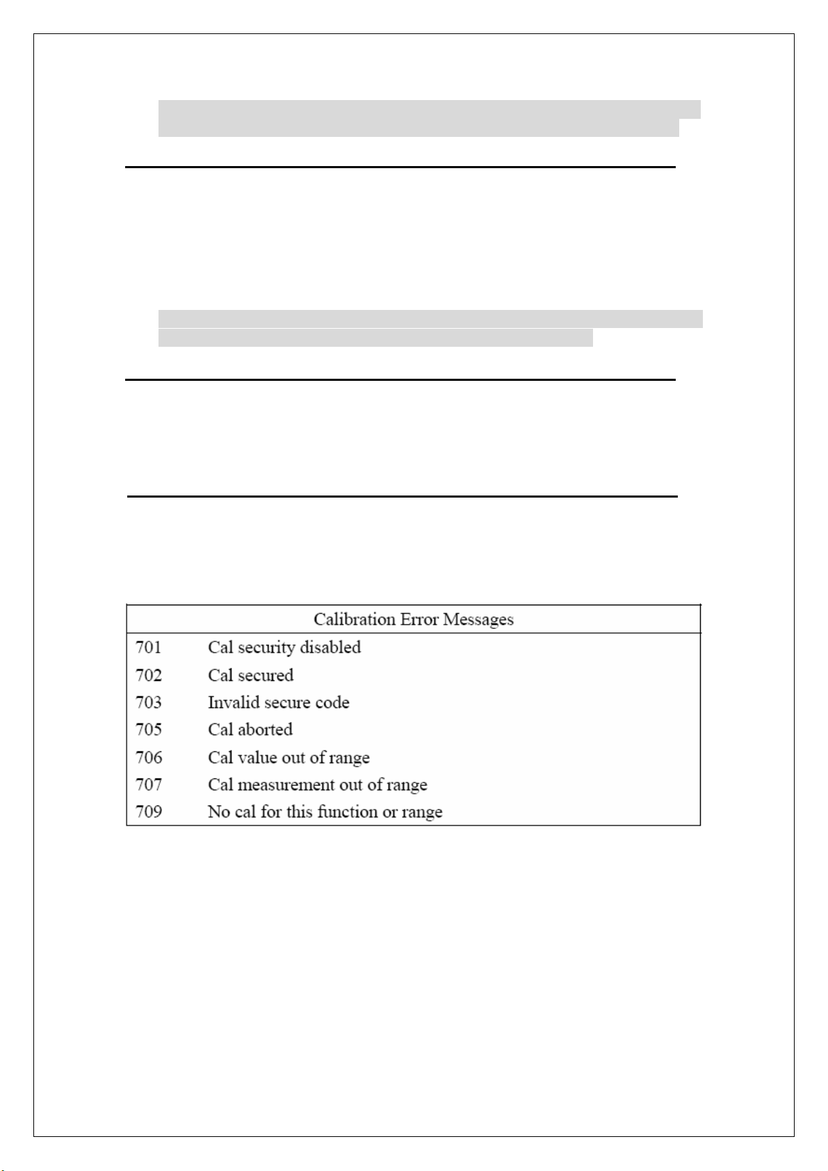
z Note 3: The Unit, which hasn’t been calibrated manually yet, must be
finished by zero adjustment, or the Error Code +720 will be shown.
6.4 Calibration Count
The calibration count will be increased from finishing calibration each time.
According to the calibration procedures on various points, a full calibration
will generate the count number more than one, and it will be recorded in the
permanent memory of the M3500A.
z Note 4: The factory default for each M3500A is 0. If the count number
exceeds 32767. The number will turn into 0.
6.5 Calibration Date
The M3500A will record a calibrated and a future calibration dates as the
factory default. Please note that the dates are not allowed to be revised.
6.6 The Calibration Error Messages
Please take a look at the following messages (Table-2) as calibration errors
occur.
Table-2
88

Appendix
±
±
Ω
Ω
±
±
Ω
Ω
Ω
A. Specification List
DC Characteristics
Function Range
Input
Resistance
24 hours accuracy
(% of reading+% of
range)(23
o
C±1oC)
1 year accuracy
(% of reading+% of
range)(23
o
C ± 5oC)
100.0000
mV
1.000000 V >10 GΩ 0.0020+0.0006 0.0040+0.0007
DCV
(DC
10.00000 V >10 GΩ 0.0015+0.0004 0.0035+0.0005
Voltage)
100.0000 V 10 MΩ 0.0020+0.0006 0.0045+0.0006
1000.000 V 10 M
Function Range
10.00000
mA
>10 G
0.0020+0.0006 0.0045+0.0010
Shunt
Resistance
10.1
0.0030+0.0030 0.0050+0.0035
1 year accuracy
24 hours accuracy
(% of reading+% of
range)(23
o
C±1oC)
(% of reading+% of
range)(23
o
C ± 5oC)
0.005+0.010 0.050+0.020
DCI
(DC
Current)
100.0000
mA
10.1
0.01+0.004 0.050+0.005
1.000000 A 0.1 Ω 0.05+0.006 0.100+0.010
3.00000 A 0.1
0.10+0.020 0.120+0.020
89

DC Characteristics (continued)
±
±
μ
μ
μ
±
±
Function Range
Test
Current
24 hours accuracy
(% of reading+% of
range)(23
o
C±1oC)
1 year accuracy
(% of reading+% of
range)(23
o
C ± 5oC)
Resistance
(Specifications
are for both 2W
and 4W when a
NULL operation
is used)
100.0000
Ω
1.000000
Ω
K
10.00000
K
Ω
100.0000
Ω
K
1.000000
Ω
M
10.00000
Ω
M
100.0000
Ω
M
1 mA 0.0030+0.0030
1 mA 0.0020+0.0005
100
10
5
A
A
A
0.0020+0.0005
0.0020+0.0005
0.002+0.001 0.010+0.001
500 nA 0.015+0.001 0.040+0.001
500 nA//10
MΩ
0.300+0.010 0.800+0.010
0.010+0.004
0.010+0.001
0.010+0.001
0.010+0.001
Diode Test 1.0000 V 1 mA 0.002+0.010 0.010+0.020
Continuity
1000.00
Ω
K
1 mA 0.002+0.010 0.010+0.020
Period (Frequency) Characteristics
Function Range
Frequency
(Hz)
3 – 5 0.10 0.10
5 – 10 0.05 0.05
10 – 40 0.03 0.03
Period
100 mV
to
750 V
40 – 300K 0.006 0.01
24 hours accuracy
(% of reading+% of
range)(23
o
C±1oC)
1 year accuracy
(% of reading+% of
range)(23
o
C ± 5oC)
90

AC Characteristics
Function Range
100.0000
mV
50K – 100K
ACV
100K–300K
(AC RMS
Voltage)
Frequency
(Hz)
24 hours accuracy ±
(% of reading+% of
range)(23
o
C±1oC)
1 year accuracy ±
(% of reading+% of
range)(23
o
C ± 5oC)
3 – 5 1.00+0.03 1.00+0.04
5 – 10 0.35+0.03 0.35+0.04
10 – 20K 0.04+0.03 0.06+0.04
20K – 50K 0.10+0.05 0.12+0.05
0.55+0.08 0.60+0.08
4.00+0.50 4.00+0.50
3 – 5 1.00+0.02 1.00+0.03
5 – 10 0.35+0.02 0.35+0.03
ACI
(AC RMS
Current)
1.000000 V
to
750.000 V
1.000000 A
3.00000 A
10 – 20K 0.04+0.02 0.06+0.03
20K – 50K 0.10+0.04 0.12+0.05
50K – 100K
100K–300K
0.55+0.08 0.60+0.08
4.00+0.50 4.00+0.50
3 – 5 1.00+0.04 1.00+0.04
5 – 10 0.30+0.04 0.30+0.04
10 – 5K 0.10+0.04 0.10+0.04
3 – 5 1.10+0.06 1.10+0.06
5 – 10 0.35+0.06 0.35+0.06
10 – 5K 0.15+0.06 0.15+0.06
(※Note 1: Specifications are for 2-hour warm-up at 6.5 Digits, slow ac filter
with Bandwidth 3Hz, sine wave input.)
(※Note 2: 750Vac range limited to 100 KHz)
91

2
B. General Specifications
item Limitation & description
Power Supply
Power Line Frequency
Power Consumption 25 VA peak (16 W average)
Operating Environment
Operating Humidity
Storage Temperature
Operating Altitude Up to 2000m
Bench Dimensions
(WxHxD)
Weight 4.36 kg
Safety
EMC
100V/120V/220V/240V ± 10%
50~60 Hz ± 10%
5 ℃ to 40 ℃
Maximum relative humidity 80% for temperature
up to 31 ℃ decreasing linearly to 50% relative
humidity at 40℃
- 40 ℃ to 70 ℃
85mm x 210mm x 350mm
IEC61010-1:2001/EN61010-1:2001 (2
UL61010-1:2004
Measurement CAT II 600V, CAT I 1000V
Pollution Degree 2
EN61326:1997+A1:1998+A2:2001+A3:2003
EMI:
CISPR 11:1997+A1:1999+A2:2002 Class B
IEC61000-3-2:2000
IEC61000-3-3:1994+A1:2001
EMS:
IEC61000-4-2:1995+A1:1998+A2:2000
IEC61000-4-3:2002
IEC61000-4-4:2004
IEC61000-4-5:1995+A1:2000
IEC61000-4-6:1996+A1:2000
IEC61000-4-8:1993+A1:2000
IEC61000-4-11:1994+A1:2000
nd
Edition)
9

3
C. Power-ON and Reset State
Function Default
Function DCV
Autozero On
Frequency and Period Source AC Voltage
Output Format ASCII
Ratio Off
AC Bandwidth Input Frequency 20Hz
AC Digits 5 ½
Voltage
Current
Frequency and
Period
Diode Test
Resistance
(2-wire)
DC digits Slow 5 ½ (1 PLC)
Range Auto
AC Digits 5 ½
DC Digits Slow 5 ½ (1 PLC)
Range Auto
Digits 5 ½
Range AUTO
Rate Medium (100ms)
Digits 5 ½
Range 1mA
Rate 0.1 PLC
Digits Slow 5 ½ (1 PLC)
Range Auto
Digits Slow 6 ½ (10 PLC)
Temperature
Thermocouple Universal Type
Source Immediate
Triggers
Delay Auto
Input Resistance 10MΩ
9

4
Conformity with the following European Directives:
The product herein conforms with the requirements of the Low Voltage Directive
73/23/EEC and the EMC Directive 89/336/EEC (including 93/68/EEC) and goes with
the CE Marking accordingly.
Conformity with the following product standards:
22 Aug. 2005
Date Hawk Shang
General Manager
For more information, please contact your local supplier, sales office or distributor.
9

5
*
a. Using continuous integrating A/D converter.
b. Input bias current: less than 30 pA at 25º C.
c. Input protection: 100 V, all range.
*
a. Specifications are for 4-wire ohms. For 2-wire ohms, use Math Null function or add 0.2
ohms for additional uncertainty.
b. Max. Lead Resistance: 10% of range per lead for 100Ω and 1KΩ ranges; 1kΩ per lead for
all other ranges.
c. Input protection: 1000 V, all ranges.
※Note: 24-hour measurement is relative to calibration accuracy.
9
 Loading...