


phyCORE-ADuC812
Hardware Manual
Edition February 2003
A product of a PHYTEC Technology Holding company

phyCORE-AduC812
In this manual are descriptions for copyrighted products that are not explicitly
indicated as such. The absence of the trademark () and copyright () symbols
does not imply that a product is not protected. Additionally, registered patents and
trademarks are similarly not expressly indicated in this manual.
The information in this document has been carefully checked and is believed to be
entirely reliable. However, PHYTEC Meßtechnik GmbH assumes no
responsibility for any inaccuracies. PHYTEC Meßtechnik GmbH neither gives any
guarantee nor accepts any liability whatsoever for consequential damages resulting
from the use of this manual or its associated product. PHYTEC Meßtechnik
GmbH reserves the right to alter the information contained herein without prior
notification and accepts no responsibility for any damages which might result.
Additionally, PHYTEC Meßtechnik GmbH offers no guarantee nor accepts any
liability for damages arising from the improper usage or improper installation of
the hardware or software. PHYTEC Meßtechnik GmbH further reserves the right
to alter the layout and/or design of the hardware without prior notification and
accepts no liability for doing so.
Copyright 2003 PHYTEC Meßtechnik GmbH, D-55129 Mainz.
Rights - including those of translation, reprint, broadcast, photomechanical or
similar reproduction and storage or processing in computer systems, in whole or in
part - are reserved. No reproduction may occur without the express written consent
from PHYTEC Meßtechnik GmbH.
EUROPE NORTH AMERICA
Address: PHYTEC Technologie Holding AG
Robert-Koch-Str. 39
D-55129 Mainz
GERMANY
Ordering
Information:
Technical
Support:
Fax: +49 (6131) 9221-33 1 (206) 780-9135
Web Site: http://www.phytec.de http://www.phytec.com
+49 (800) 0749832
order@phytec.de
+49 (6131) 9221-31
support@phytec.de
PHYTEC America LLC
203 Parfitt Way SW, Suite G100
Bainbridge Island, WA 98110
USA
1 (800) 278-9913
info@phytec.com
1 (800) 278-9913
support@phytec.com
3rd Edition: February 2003
PHYTEC Meßtechnik GmbH 2003 L-461e_3

Table of Contents
Preface ......................................................................................................1
1 Introduction .........................................................................................3
1.1 Block Diagram..............................................................................6
1.2 View of the phyCORE-ADuC812................................................7
2 Pin Description.....................................................................................9
3 Jumpers..............................................................................................17
3.1 J2 Supply Voltage SRAMs........................................................20
3.2 J1, J9, J11 SRAM Memory Capacity.........................................20
3.3 J3, J4, J12 Serial Interface.........................................................21
3.4 J5 Interrupt Output of the CAN Controller ...............................22
3.5 J6 Internal or External Program Memory..................................22
3.6 J7 Interrupt Output of the RTC..................................................23
3.7 J8 CAN Interface.......................................................................23
3.8 J13, J14 I²C Bus Signals SDATA/MOSI and SCLOCK............24
4 Memory Model...................................................................................25
4.1 Memory Model Following Reset................................................26
4.2 Runtime Model...........................................................................27
4.3 Von Neumann Model .................................................................29
4.4 Programming Model...................................................................31
4.5 Control Register 1.......................................................................33
4.6 Address Register.........................................................................38
4.7 Mask Register.............................................................................39
4.8 Control Register 2.......................................................................42
4.9 Input Register 1...........................................................................42
4.10 Output Register 1........................................................................43
5 Serial Interfaces.................................................................................45
5.1 RS-232 Interface.........................................................................45
5.2 RS-485 Interface.........................................................................45
5.3 CAN Interface.............................................................................46
6 Flash Memory....................................................................................49
6.1 On-Board Flash Memory (U4) ...................................................49
6.2 On-Chip Flash Memory..............................................................51
7 Serial EEPROM (U11)......................................................................52
PHYTEC Meßtechnik GmbH 2003 L-461e_3

phyCORE-AduC812
8 Real-Time Clock RTC-8563 (U12)...................................................53
9 Reset Controller (U6)........................................................................54
10 Remote Supervisor Chip (U7)..........................................................55
11 Battery Buffer....................................................................................56
12 A/D Converter and D/A Converter .................................................57
13 Technical Specifications....................................................................59
14 Hints for Handling the Module........................................................61
15 The phyCORE-ADuC812 on the phyCORE Development
Board LD 5V......................................................................................63
15.1 Concept of the phyCORE Development Board LD 5V .............63
15.2 Development Board LD 5V Connectors and Jumpers...............65
15.2.1 Connectors.....................................................................65
15.2.2 Jumpers on the phyCORE Development
Board LD 5V.................................................................66
15.2.3 Unsupported Features and Improper Jumper Settings ..68
15.3 Functional Components on the phyCORE Development
Board LD 5V..............................................................................69
15.3.1 Power Supply at X1.......................................................69
15.3.2 Starting FlashTools .......................................................71
15.3.3 First Serial Interface at Socket P1A..............................73
15.3.4 Socket P1B....................................................................74
15.3.5 CAN Interface at Plug P2A...........................................76
15.3.6 RS-485 Interface at Plug P2B .......................................82
15.3.7 Programmable LED D3.................................................84
15.3.8 Pin Assignment Summary of the phyCORE, the
Expansion Bus and the Patch Field...............................85
15.3.9 Battery Connector BAT1...............................................92
15.3.10 DS2401 Silicon Serial Number.....................................92
15.3.11 Pin Header Connector X4 .............................................93
16 Revision History................................................................................94
Index ....................................................................................................95
PHYTEC Meßtechnik GmbH 2003 L-461e_3

Index of Figures and Tables
Figure 1: Block Diagram phyCORE-ADuC812 ..........................................6
Figure 2: View of the phyCORE-ADuC812 (Top View) ............................7
Figure 3: View of the phyCORE-ADuC812 (Bottom View).......................8
Figure 4: Pinout of the phyCORE-Connector (Component Side)................9
Figure 5: Numbered Matrix Overview of the phyCORE-Connector
(Viewed from Above).................................................................11
Figure 6: Numbering of the Jumper Pads...................................................17
Figure 7: Location of the Jumpers (Top View)..........................................17
Figure 8: Location of the Jumpers (Bottom View)....................................18
Figure 9: Memory Model Following Hardware Reset...............................26
Figure 10: Runtime Model ...........................................................................28
Table of Contents
Figure 11: Von Neumann Model .................................................................30
Figure 12: Programming Model...................................................................32
Figure 13: Flash Programming Model .........................................................34
Figure 14: Configuration of the I/O Area ....................................................35
Figure 15: Example of a Memory Model.....................................................41
Figure 16: Flash Memory Banks..................................................................50
Figure 17: Physical Dimensions (Not Shown at Scale) ...............................59
Figure 18: Modular Development and Expansion Board Concept
with the phyCORE-ADuC812....................................................64
Figure 19: Location of Connectors on the phyCORE Development
Board LD 5V ..............................................................................65
Figure 20: Numbering of Jumper Pads ........................................................66
Figure 21: Location of the Jumpers (View of the Component Side)...........67
Figure 22: Default Jumper Settings of the phyCORE Development
Board LD 5V with phyCORE-ADuC812...................................67
Figure 23: Connecting the Supply Voltage at X1 ........................................70
PHYTEC Meßtechnik GmbH 2003 L-461e_3

phyCORE-AduC812
Figure 24: Pin Assignment of the DB-9 Socket P1A as RS-232
(Front View)...............................................................................73
Figure 25: Pin Assignment of the DB-9 Socket P1B (Front View).............74
Figure 26: Pin Assignment of the DB-9 Plug P2A (CAN Transceiver on
phyCORE-ADuC812, Front View)............................................ 76
Figure 27: Pin Assignment of the DB-9 Plug P2A
(CAN Transceiver on Development Board)............................... 78
Figure 28: Pin Assignment of the DB-9 Plug P2A
(CAN Transceiver on Development Board with Galvanic
Separation)..................................................................................81
Figure 29: Pin Assignment of the DB-9 Plug P2B as RS-485 Interface .....82
Figure 30: Pin Assignment Scheme of the Expansion Bus..........................86
Figure 31: Pin Assignment Scheme of the Patch Field................................86
Figure 32: Connecting the DS2401 Silicon Serial Number.........................93
Figure 33: Pin Assignment of the DS2401 Silicon Serial Number..............93
Table 1: Pinout phyCORE-Connector A/B (ADuC812, ADuC824)........ 12
Table 2: Pinout phyCORE-Connector C/D (ADuC812, ADuC824)........ 13
Table 3: Pinout phyCORE-Connector E/F (ADuC812, ADuC824).........14
Table 4: Pinout phyCORE-Connector G/H (ADuC812).......................... 15
Table 5: Pinout phyCORE-Connector G/H (ADuC824).......................... 15
Table 6: Jumper Description.....................................................................19
Table 7: J2 Supply Voltage Configuration for SRAMs U5/U13.............20
Table 8: J1, J9, J11 SRAM Capacity Configuration ...............................20
Table 9: J3, J4 and J12 Serial Interface Configuration............................21
Table 10: J5 CAN Controller Interrupt Output Configuration..................22
Table 11: J6 Access to External or Internal Program Memory................. 22
Table 12: J7 RTC Interrupt Output Configuration.................................... 23
Table 13: J8 CAN Interface Configuration ...............................................24
Table 14: J13 und J14 I²C Interface Configuration...................................24
Table 15: Control Register 1 of the Address Decoder................................33
PHYTEC Meßtechnik GmbH 2003 L-461e_3

Table of Contents
Table 16: Address Register of the Address Decoder..................................38
Table 17: Mask Register of the Address Decoder......................................39
Table 18: Example of Address Decoder Functions ....................................40
Table 19: Control Register 2 of the Address Decoder................................42
Table 20: Input Register 1 of the Address Decoder....................................42
Table 21: Output Register 1 of the Address Decoder.................................43
Table 22: Memory Device Options at U11.................................................52
Table 23: Improper Jumper Settings for the Development Board..............68
Table 24: JP9, JP36 Configuration of the Supply Voltages VCCI
and AVCC ..................................................................................69
Table 25: JP9, JP36 Improper Jumper Settings for the
Supply Voltages..........................................................................70
Table 26: JP28 Configuration of the Boot Button......................................71
Table 27: JP28 Configuration of a Permanent FlashTools
Start Condition............................................................................72
Table 28: JP22, JP23, JP10 Configuration of Boot via RS-232 .................72
Table 29: Improper Jumper Settings for Boot via RS-232.........................72
Table 30: Jumper Configuration for the RS-232 Interface.........................73
Table 31: Jumper Configuration of the DB-9 Socket P1B.........................74
Table 32: Improper Jumper Settings for Configuration of P1B .................75
Table 33: Jumper Configuration for CAN Plug P2A using the CAN
Transceiver on the phyCORE-ADuC812...................................76
Table 34: Improper Jumper Settings for the CAN Plug P2A
(CAN Transceiver on phyCORE-ADuC812).............................77
Table 35: Jumper Configuration for CAN Plug P2A using the CAN
Transceiver on the Development Board.....................................78
Table 36: Improper Jumper Settings for the CAN Plug P2A
(CAN Transceiver on the Development Board).........................79
Table 37: Jumper Configuration for CAN Plug P2A using the CAN
Transceiver on the Development Board with
Galvanic Separation....................................................................80
PHYTEC Meßtechnik GmbH 2003 L-461e_3

phyCORE-AduC812
Table 38: Improper Jumper Settings for the CAN Plug P2A
(CAN Transceiver on Development Board with Galvanic
Separation)..................................................................................81
Table 39: Jumper Configuration for DB-9 Plug P2B as
RS-485 Interface.........................................................................82
Table 40: Improper Jumper Settings for the RS-485 Interface at
Plug P2B.....................................................................................83
Table 41: JP17 Configuration of the Programmable LED D3 ...................84
Table 42: Pin Assignment Data/Address Bus for the
phyCORE-ADuC812 / Development Board /
Expansion Board ........................................................................87
Table 43: Pin Assignment Control Signals for the
phyCORE-ADuC812 / Development Board /
Expansion Board ........................................................................88
Table 44: Pin Assignment Interface Signals for the
phyCORE-ADuC812 / Development Board /
Expansion Board ........................................................................88
Table 45: Pin Assignment Input and Output Port for the
phyCORE-ADuC812 / Development Board /
Expansion Board ........................................................................89
Table 46: Pin Assignment Analog Signal Row on the
phyCORE-ADuC812 / Development Board /
Expansion Board ........................................................................89
Table 47: Pin Assignment Analog Signal Row on the
phyCORE-ADuC824 / Development Board /
Expansion Board ........................................................................90
Table 48: Unused Pins on the phyCORE-ADuC812 /
Development Board / Expansion Board..................................... 90
Table 49: Pin Assignment Power Supply for the
phyCORE-ADuC812 / Development Board /
Expansion Board ........................................................................91
Table 50: JP19 Jumper Configuration for Silicon Serial Number Chip.....92
PHYTEC Meßtechnik GmbH 2003 L-461e_3

Preface
This phyCORE-ADuC812 Hardware Manual describes the board’s
design and functions. Precise specifications for the Analog Devices
ADuC812 or ADuC824 microcontroller can be found in the enclosed
microcontroller Data Sheet/User’s Manual. If software is included
please also refer to additional documentation for this software.
In this hardware manual and in the attached schematics, low active
signals are denoted by a "/" in front of the signal name (i.e.: /RD). A
"0" indicates a logic-zero or low-level signal, while a "1" represents a
logic-one or high-level signal.
Declaration of Electro Magnetic Conformity for the
PHYTEC phyCORE-ADuC812
Preface
PHYTEC Single Board Computers (henceforth products) are designed
for installation in electrical appliances or as dedicated Evaluation
Boards (i.e.: for use as a test and prototype platform for
hardware/software development) in laboratory environments.
Note:
PHYTEC products lacking protective enclosures are subject to damage by Electro Static Discharge (ESD) and, hence, may only be
unpacked, handled or operated in environments in which sufficient
precautionary measures have been taken in respect to ESD dangers. It
is also necessary that only appropriately trained personnel (such as
electricians, technicians and engineers) handle and/or operate these
products. Moreover, PHYTEC products should not be operated
without protection circuitry if connections to the product’s pin header
rows are longer than 3 m.
PHYTEC Meßtechnik GmbH 2003 L-461e_3 1

phyCORE-AduC812
PHYTEC products fulfill the norms of the European Union’s
Directive for Electro Magnetic Conformity only in accordance to the
descriptions and rules of usage indicated in this hardware manual
(particularly in respect to the pin header row connectors, power
connector and serial interface to a host-PC).
Implementation of PHYTEC products into target devices, as well as
user modifications and extensions of PHYTEC products, is subject to
renewed establishment of conformity to, and certification of, Electro
Magnetic Directives. Only after doing so the devices are allowed to
be put into circulation.
The phyCORE-ADuC812 is one of a series of PHYTEC Single Board
Computers (SBCs) that can be fitted with different controllers and,
hence, offers various functions and configurations. PHYTEC supports
all common 8- and 16-bit controllers in two ways:
(1) as the basis for Rapid Development Kits which serve as a
reference and evaluation platform
(2) as insert-ready, fully functional micro- / mini- and phyCORE
OEM modules which can be embedded directly into the user's
peripheral hardware design.
PHYTEC's microcontroller modules allow engineers to shorten development horizons, reduce design costs and speed project concepts from
design to market.
2 PHYTEC Meßtechnik GmbH 2003 L-461e_3

1 Introduction
The phyCORE-ADuC812 belongs to PHYTEC’s phyCORE Single
Board Computer (SBC) module family. The phyCORE SBCs
represent the continuous development of PHYTEC Single Board
Computer technology. Like its mini-, micro- and nanoMODUL
predecessors, the phyCORE boards integrate all core elements of a
microcontroller system on a subminiature board and are designed in a
manner that ensures their easy expansion and embedding in peripheral
hardware developments.
As independent research indicates that approximately 70 % of all
Electro Magnetic Interference (EMI) problems stem from insufficient
supply voltage grounding of electronic components in high frequency
environments the phyCORE board design features an increased pin
package. The increased pin package allows dedication of
approximately 20 % of all pin header connectors on the phyCORE
boards to ground. This improves EMI and EMC characteristics and
makes it easier to design complex applications meeting EMI and
EMC guidelines using phyCORE boards even in high noise
environments.
Introduction
phyCORE boards achieve their small size through advanced SMD
technology and multi-layer design. In accordance with the complexity
of the module, 0402-packaged SMD and laser-drilled Microvias
components are used on the boards, providing phyCORE users with
access to this cutting edge miniaturization technology for integration
into their own design.
The phyCORE-ADuC812 is a universal microcontroller board in
subminiature dimensions (55 mm x 60 mm). It can be populated with
ADuC812 and ADuC824 microcontrollers from Analog Device. The
ADuC812 has an integrated reference voltage source, a temperature
sensor, two 12-bit D/A-converters and a 12-bit, 8-channel
A/D-converter.
PHYTEC Meßtechnik GmbH 2003 L-461e_3 3

phyCORE-AduC812
The ADuC824 has an integrated reference voltage source, a
temperature sensor, a 24-bit and a 16-bit A/D-converter with a total of
5 channels and a 12-bit D/A-converter.
The universal design enables easy integration of the
phyCORE-ADuC812 into many applications. Since all controlers
signals and in- and outputs extend to 2.54 mm pin header rows on the
edge of the board, the phyCORE-ADuC812 can be inserted like a big
chip into your target application.
Precise specifications for the controller populating the board can be
found in the applicable controller User’s Manual or Data Sheet. The
descriptions in this manual are based on the ADuC812 controller. No
description of compatible microcontroller derivative functions is
included, as such functions are not relevant for the basic functioning
of the phyCORE-ADuC812.
4 PHYTEC Meßtechnik GmbH 2003 L-461e_3

The phyCORE-ADuC812 offers the following features:
• subminiature Single Board Computer (55 mm x 60 mm) achieved
through advanced SMD technology
• Analog Device microcontrollers with 8 kByte of on-chip Flash for
Code and 640 Bytes of EEPROM Flash for data
• integrated reference voltage and temperature sensor
• the ADuC812 microcontroller features two 12-bit D/A-converters
and a 12-bit, 8-channel AD converter
• the ADuC824 microcontroller features one 12-bit D/A-converter, a
24-bit and a 16-bit A/D-converter with 5 channels.
• improved interference protection through multi-layer technology
as well as reduced radiation interference resulting from improved
ground connections
• all digital ports as well as data and address lines extend to pin
header rows available at the edge of the board
Introduction
• the analog inputs and outputs can be accessed over their specific
pin header connector
• can be inserted into target circuitry like a big chip
• 128 kByte to 1 MB SRAM on-board (SMD)
• 128 kByte to 512 kByte external Flash on-board(SMD)
1
1
• on-board Flash programming with FlashTools
• no separate programming voltage necessary because of 5 V Flash
devices
• flexible address decoding, configurable with software via complex
logic devices
• Bank latches for the Flash are integrated into the address decoder
• linear access to 16 MB data via an additional pointer in the
microcontroller
• selectable RS-232 or RS-485 interface
• optional CAN interface with SJA1000 and CAN transceiver
82C251
• I²C-Real-Time Clock
• optional 2 to 8 kByte I²C-EEPROM
1
: North America: Support Hotline: + 1-800-278-9913 http://www.phytec.com
Europe: Support Hotline: 0 800-0-749-832
PHYTEC Meßtechnik GmbH 2003 L-461e_3 5
http://www.ph ytec.de

phyCORE-AduC812
s
p
• Reset logic and battery monitoring
• Remote Supervisory Circuit
2
• free Chip Select signals for connection of external peripheries
• I/O port expansion with 8 TTL-inputs and 8 TTL-outputs
• requires a single 5 V /typ. <120 mA supply voltage
• the /EA pin can be accessed from the outside to enable easy
connection of emulators from Accutron Limited
1.1 Block Di agram
SRAM
(U5/U13)
128 kB..1 MB
1
Microcontroller
Analog Device
ADuC812
(ADuC824)
(U1)
RESET
Voltage
Supervisor
FLASH
(U4)
128
1
kB..512 kB
CAN
RxD, TxD
Remote
Supervisor
(U7)(U6)
I/O Port
(U14 Input)
(U15 Output)
RxD
Address/Data Bus
CANRx, CANTx
Digital Ports
Analog Ports
I2C Interface
RTC
(U12)
Addres
Decoder
(U2)
CAN
Transceiver
(U8)(U3)
RS-232
Transceiver
(U9)
RS-485
Transceiver
(U10)
EEPROM
(U11)
/CS[3..1]
/CS_Ext
h
CAN
y
C
O
R
RS-232
E
C
RS-485
o
n
n
e
c
t
o
r
42
1 phyCORE specific
2 This feature is under development and is not available yet.
Figure 1: Block Diagram phyCORE-ADuC812
2
: This feature is under development and not available yet.
6 PHYTEC Meßtechnik GmbH 2003 L-461e_3

1.2 View of the phyCORE-ADuC812
Introduction
PIN 1 A
1
2
3
4
5
6
7
8
9
10
11
12
13
14
15
16
17
18
19
R8
D3
BFEDC
D2
R2
Q3
345
G
H
C20
CB57
TP1
CB53
R18
J9 J10 J2
R19
CB10
U1
U4
U5
CB59
6
789101112
C8
CB7
CB8
C13
C5
C15
D1
XT2
C12
C9
C10
C11
CB9
C19
CB58
C16
XT1
J7 J5 J8
R13
R12
C23
R
24
R23
R22
Q5
J12
J4
J3
J6
R9 R10
U9
U15
U12
CB56
R25
CB60
R20
J13
1
2
3
4
5
6
7
8
9
10
11
12
13
14
15
16
17
18
19
J14
U11
Figure 2: View of the phyCORE-ADuC812 (Top View)
PHYTEC Meßtechnik GmbH 2003 L-461e_3 7

phyCORE-AduC812
1
2
3
4
5
6
7
8
9
10
11
12
13
14
15
16
17
18
19
CB1
CB4
Q6
RN2
R16
R27
U6
R26
U10
U8
CB52
R17
U3
C2
R11
R5
U14
R6
Q2
CB51
C
24
Q4
R7
R21
C21
R1
C18
C17
R7
CB5
R35
R29
R30
CB2
R36
R37
CB6
789101112
C40
Q1
CB3
R3
C14
J11 J1
C41
6
C3
RN1
U13
C7
U2
R31
R28
345
R34
CB54
U7
C4
C1
CB55
R32
R33
PIN 1
1
2
3
4
5
6
7
8
9
10
11
12
13
14
15
16
17
18
19
Figure 3: View of the phyCORE-ADuC812 (Bottom View)
8 PHYTEC Meßtechnik GmbH 2003 L-461e_3

2 Pin Description
Please note that all module connections are not to exceed their
expressed maximum voltage or current. Maximum signal input values
are indicated in the corresponding controller User’s Manual/Data
Sheets. As damage from improper connections varies according to use
and application, it is the user's responsibility to take appropriate safety
measures to ensure that the module connections are protected from
overloading through connected peripherals.
As the Figure 4 indicates, all controller signals extend to standardwidth (2.54 mm) pin rows lining two sides the board (referred to as
phyCORE-connector). This allows the board to be plugged into any
target application like a "big chip".
Pin Description
CLKOUT
CLKIN
/INT1 GND
NC
/CS2
/RD
A0
A3
A5
A7
A16A8
A18A10
A20A12
A21A13
A23A15
AD1
AD3
AD6
A16
A19 GND
A21
A23
/INT0
NC
GND /CS1
ALE
/CS3
GND
/WR
A1
A2
GND
A4
GND
A6
A17A9
GND
A19A11
A22A14
GND
AD0
GND AD2
AD4
AD5
GND
AD7
A17
A18
A20
GND
A22
/EA
NC
PIN 1 A
1
2
3
4
5
6
7
8
9
10
11
12
13
14
15
16
17
18
19
ADC1 IEXC1
T2 AGND
AGND VREF T2EXT IEXC2 VREF- ADC4 /SSAGND
DAC0 ADC2
ADC0 AGND
AGND VREF ADC1 ADC3 CREF ADC5 ADC6AGND
BFEDC
345
AVCC ADC3 AGND /MISO ADC2
VREF+
AVCC ADC4 AGND ADC7 DAC1
VREF
6
789101112
G
H
AGND
AGND
ADuC824
ADuC812
1
2
3
4
5
6
7
8
9
10
11
12
13
14
15
16
17
18
19
VCC
VCC
NC
NC
NC
NC
VBAT
VPD PFI
WDI
GND
BOOT
/RES /RES
GND
T0
GND
T1
IN2
IN1
GND
IN4
RxD
TxD
CANTxD GND
GND
CANRxD
A
CANL
GND
CANH
SCL
SDA
GND
OUT1
GND OUT4
OUT3
OUT6
OUT5
GND
GND
GND
PFO
NC
IN0
IN3
IN5
IN6
IN7
B
TxD0
RxD0
OUT0
OUT2
OUT7
NC
NC
Figure 4: Pinout of the phyCORE-Connector (Component Side)
PHYTEC Meßtechnik GmbH 2003 L-461e_3 9

phyCORE-AduC812
A new numbering scheme for the pins on the phyCORE-connector
has been introduced with the phyCORE specifications. This enables
quick and easy identification of desired pins and minimizes errors
when matching pins on the phyCORE module with the receptacle
socket on the appropriate PHYTEC phyCORE Development
Board LD 5V or your OEM application.
The numbering scheme for the phyCORE-connector is based on a two
dimensional matrix in which column positions are identified by a
letter and row position by a number. Pin 1A, for example, is always
located in the upper left hand corner of the matrix. The pin numbering
values increase moving down on the board. Lettering of the pin
connector rows progresses alphabetically from left to right
(refer to Figure 5).
The numbered matrix can be aligned with the phyCORE-ADuC812
(viewed from above; phyCORE-connector header pins pointing
down) or with the socket of the phyCORE Development
Board LD 5V / target circuitry. The upper left hand corner of the
numbered matrix (Pin 1A) is thus covered with the corner of the
phyCORE-ADuC812 marked with a white triangle. The numbering
scheme is always in relation to the PCB as view e d from above, even if
all contacts extend to the bottom of the board.
The numbering scheme is thus consistent for both the module’s
phyCORE-connector as well as mating connectors on the phyCORE
Development Board LD 5V or target hardware, thereby considerably
reducing the risk of pin identification errors.
Since the pins are exactly defined according to the numbered matrix
previously described, the phyCORE-connector’s receptacle socket is
usually assigned a single designator for its position (X1 for example).
In this manner the phyCORE-connector comprises a single, logical
unit regardless of the fact that it could consist of more than one
physical connector. The location of row 1 on the board is marked by a
white triangle on the PCB to allow easy identification.
10 PHYTEC Meßtechnik GmbH 2003 L-461e_3

The following figure (see Figure 5) illustrates the numbered matrix
system. It shows a phyCORE-ADuC812 mounted on a phyCORE
Development Board LD 5V. The shaded area of the phyCOREconnectors shown below indicates the remaining pins not used in
conjunction with the phyCORE-ADuC812 which, when plugged onto
the Development Board, does not span the entire length of the
receptacle socket. The phyCORE Development Board LD 5V can
house all phyCORE modules with standard-width (2.54 mm / 0.10 in.)
pin header rows and a maximum of 32 pins per pin header row, A, B,
C, D, E and F.
Pin Description
A B C
1
1
14
G
H
D E F
1
Figure 5: Numbered Matrix Overview of the phyCORE-Connector
(Viewed from Above)
Many of the controller port pins accessible at header pins along the
edges of the board have been assigned alternate functions that can be
activated via software.
PHYTEC Meßtechnik GmbH 2003 L-461e_3 11
phyCORE-AduC812
The following tables provide an overview of the pinout of the
phyCORE-connector and shows possible alternative functions of the
pins. Please refer to the microcontroller User’s Manual/Data Sheet
for details on the functions and features of controller signals and port
pins.
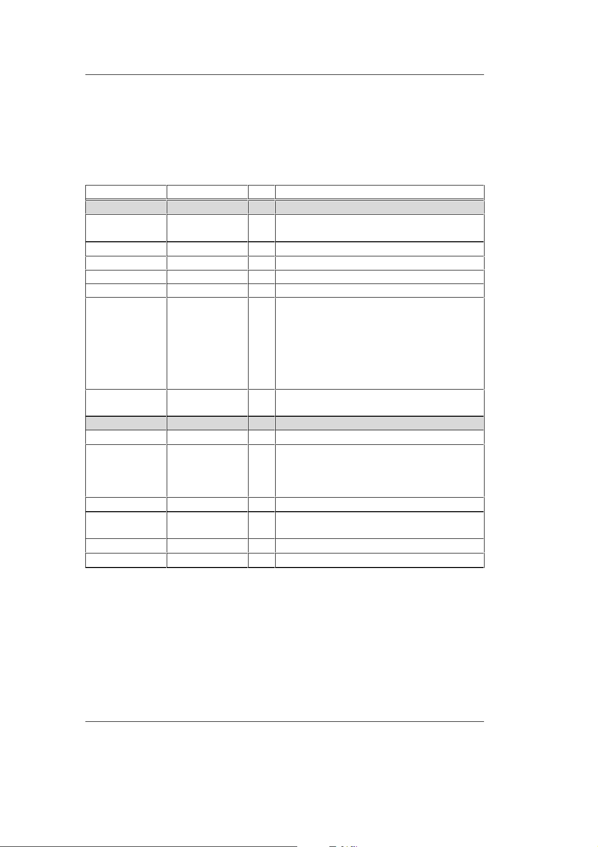
Pin Number Signal I/O Comments
Pin Row X1A
1A ClkIn I Optional external clock generator,
connected directly to XTAL1 of the µC
2A P3.3 (/INT1) I/O
3A NC Not used
4A /CS2 O Pre-decoded Chip Select signal #2
5A /RD O /RD signal
6A, 7A,
8A, 9A,
10A,
11A,
12A,
16A, 17A,
A18A, 19A
13A, 14A,
15A
Pin Row X1B
1B ClkOut -
2B, 3B, 5B, 7B,
8B, 10B, 12B,
13B, 15B,
17B, 18B
4B ALE O
6B, 9B,
11B,16B
14B AD4 I/O
19B /EA I
A0, A3,
A5, A7,
A18A10,
A20A12,
A23A15,
A16, A19,
A21, A23
AD1, AD3,
AD6
GND - Ground 0 V
A1, A16A8,
A21A13, A17
Port pin µC
O
Address line of µC or of the address latch
O
Address/data line of µC
Connected directly to XTAL2 of the µC
Address latch enable output of µC
O
Address line of µC or of the address latch
Address/data line of µC
/EA pin of µC
Table 1: Pinout phyCORE-Connector A/B (ADuC812, ADuC824)
12 PHYTEC Meßtechnik GmbH 2003 L-461e_3

Pin Description
Pin Number Signal I/O Comments
Pin Row X1C
1C P3.2 (/INT0) I/O
2C NC Not used
3C, 4C /CS1, /CS3 O Pre-decoded Chip Select signals #1, #3
5C P3.6 (/WR) I/O
6C, 7C, 8C,
9C,
10C,
11C,
16C, 17C, 18C
12C, 13C,
14C, 15C
19C NC Not used
Pin Row X1D
1D VCC - Supply voltage +5 VDC
2D, 3D NC - Not used
4D VBAT I Connector for external battery (+)
5D WDI
6D BOOT I If Boot=1 during a low to high transition of
7D,
8D
9D,10D IN1, IN4 I Digital input port
11D RxD (P3.0) I
12D CANTxD O CANTxD output of the SJA1000
13D CANRxD I CANRxD input of the SJA1000
14D CANL I/O CANL signal of the CAN transceiver
15D CANH I/O CANH signal of the CAN transceiver
16D SCL O Clock output I2C bus
17D, 18D,
19D
A2, A4, A6,
A17A9,
A19A11,
A22A14,
A18, A20, A22
AD0, AD2,
AD5, AD7
P3.4 (T0),
P3.5 (T1)
OUT1, OUT3,
OUT5
Port pin µC
/WR signal of µC
O
Address line of µC or of the address latch
I/O
Address/data line of µC
WDI input of the Reset controllers
I
the Reset signal, the Boot procedure will
start.
I/O
Port pins µC
RxD input of the µC
O Digital output port
Table 2: Pinout phyCORE-Connector C/D (ADuC812, ADuC824)
PHYTEC Meßtechnik GmbH 2003 L-461e_3 13

phyCORE-AduC812
Pin Number Signal I/O Comments
Pin Row X1E
1E VCC - Supply voltage +5 VDC
2E, 3E NC - Not used
4E VPD O Voltage output for external buffer
5E, 7E, 8E, 10E,
12E, 13E, 15E,
17E,18E
6E /RES O Reset output of the module, connected
9E IN2 I Digital input port
11E TxD (P3.1) I/O
14E A I/O Differential A signal of the RS-485
16E SDA I/O Data line I²C bus
19E OUT6 O Digital output port
Pin Row X1F
1F, 2F, 3F GND - Ground 0 V
4F PFI I Power Fail Input of Reset IC
5F /PF0 I Power Fail Output of Reset IC
6F /RES I Reset input of the module
7F NC - Not used
8F, 9F, 10F,
11F, 12F
13F B I/O Differential B signal of the RS-485
14F TxD0 I Transmitter output of the RS-232 transceiver
15F RxD0 I Receiver input of the RS-232 transceiver
16F, 17F,
18F, 19F
GND - Ground 0 V
directly to reset input
TxD output of the µC
transceiver
IN0, IN3, IN5
IN6, IN7
OUT0, OUT2
OUT4, OUT7
I Digital input port
transceiver
O Digital output port
Table 3: Pinout phyCORE-Connector E/F (ADuC812, ADuC824)
14 PHYTEC Meßtechnik GmbH 2003 L-461e_3

Pin Description
Pin Number Signal I/O Comments
Pin Row X1G
3G, 12G DAC0, DAC1 O A/D converter outputs
4G, 6G,
9G, 11G
5G,10G AGND - Analog Ground 0 V
7G VREF - Reference voltage input
8G AVCC - Analog supply voltage +5 VDC
Pin Row X1H
4H VREF - Reference voltage output
5H, 6H,
9H, 10H
7H CREF Capacitor connection for reference voltage
3H, 8H, 12H AGND - Analog Ground 0 V
11H NC - Not used
Table 4: Pinout phyCORE-Connector G/H (ADuC812)
Pin Number Signal I/O Comments
Pin Row X1G
4G T2 I/O Timer T2
6G IEXC1 I Input capacitor C1
3G, 12G,
9G
5G, 10G AGND - Analog Ground 0 V
7G VREF+ I Reference voltage input (+)
8G AVCC - Analog supply voltage +5 VDC
11G /MISO I/O /MISO für SPI Interface des Controllers
Pin Row X1H
4H VREF+ - Reference voltage input (+)
5H T2EXT I/O Control input for Timer 2
6H IEXC2 I Input capacitor C2
7H VREF- I Reference voltage input (-)
9H ADC4 I A/D converter inputs
3H, 8H, 12H AGND - Analog Ground 0 V
11H NC - Not used
ADC0, ADC2,
ADC4, ADC7
ADC1, ADC3,
ADC5, ADC6
ADC1, ADC2,
ADC3
I A/D converter inputs
I A/D converter inputs
I A/D converter inputs
Table 5: Pinout phyCORE-Connector G/H (ADuC824)
PHYTEC Meßtechnik GmbH 2003 L-461e_3 15

phyCORE-AduC812
16 PHYTEC Meßtechnik GmbH 2003 L-461e_3

3 Jumpers
For configuration purposes, the phyCORE-ADuC812 has 14 solder
jumpers, some of which have been installed prior to delivery.
Figure 6 illustrates the numbering of the jumper pads, while Figure 7
and Figure 8 indicate the location of the jumpers on the board
Jumper
1
2
3
z.B.: J3, J4, ..
z.B.: J1, J5, ..
Figure 6: Numbering of the Jumper Pads
PIN 1 A
1
2
3
4
5
6
7
8
9
10
11
12
13
14
15
16
17
18
19
BFEDC
345
G
H
U1
6
789101112
U4
U5
1
2
4
1
2
3
z.B.: J2
1
2
3
4
5
6
7
8
9
10
11
12
XT2
J7 J5 J8
J12
J4
J3
J6
13
U9
14
15
16
17
U15
18
19
J13 J1 4
J9 J10 J2
XT1 U11
Figure 7: Location of the Jumpers (Top View)
PHYTEC Meßtechnik GmbH 2003 L-461e_3 17

phyCORE-AduC812
1
2
3
4
5
6
7
8
9
10
11
12
13
14
15
16
17
18
19
U6
U8
U10
U3
U14
789101112
6
345
PIN 1
1
2
3
4
5
6
7
8
9
10
U2
11
12
13
14
15
16
17
U13
18
19
J11 J1
U7
Figure 8: Location of the Jumpers (Bottom View)
18 PHYTEC Meßtechnik GmbH 2003 L-461e_3

The jumpers (J = solder jum per) have the following functions:
Default Setting Alternative Setting
Jumper
J1
J2
J3
J4
J5
J6
J7
J8
J9
J10
J11
J12
J13
J14
(1+2) 128 kB SRAM at U5
(RAM1)
(1+2) SRAMs supplied via
VPD
(1+2) RxD connected to
RS-232 transceiver
(1+2) TxD connected to
RS-232 transceiver
(closed) CAN interrupt
connected to /INT0
(1+2) with 1 kΩ; external
program memory
(closed) RTC interrupt
connected to /INT1
(closed) on-board CAN
transceiver connected
with CANRxD
(1+2) 128 kB SRAM at U5
(RAM1)
(1+2) external memory
enabled
(1+2) 128 kB SRAM at U13
(RAM2)
(1+2) RS-485 enable signal
controlled by OUT0
(closed) PSDA line of the I²C
bus connected with
controller pin 27
(closed) PSCL line of the I²C
bus connected with
controller pin 26
(2+3) 512 kB SRAM at U5
(RAM1)
(2+3) SRAMs supplied via
VCC
(2+3) RxD connected to
RS-485 transceiver
(2+3) TxD connected to
RS-485 transceiver
(open) CAN Interrupt not
connected (polling mode)
(2+3) with 1 kΩ; internal
program memory
(open) RTC interrupt not
connected
(open) on-board CAN
transceiver disconnected
from CANRxD
(2+3) 512 kB SRAM at U5
(RAM1)
(2+3) external memory
disabled
(2+3) 512 kB SRAM at U13
(RAM2)
(2+3) RS-485 enable signal
controlled by T1
(open) PSDA line of the I²C
bus disconnected from
controller
(open) PSCL line of the I²C
bus disconnected from
controller
Table 6: Jumper Description
PHYTEC Meßtechnik GmbH 2003 L-461e_3 19

phyCORE-AduC812
3.1 J2 Supply Voltage SRAMs
Mit dem Jumper J2 wird die Versorgungsspannung der SRAMs
eingestellt. Wenn die SRAMs über die Batterie (VPD) gepuffert
werden sollen, ist J2 auf Position 1+2 zu schliessen. Ist J2 auf
Position 2+3 geschlossen, werden die SRAM Bausteine mit VCC
verbunden.
The following configurations are possible:
SRAM Supply Voltage J2
SRAMs connected to VPD, supply voltage
via battery buffer
1 + 2
*
SRAMs connected to VCC, supply voltage
2 + 3
without battery buffer
*= Default setting
Table 7: J2 Supply Voltage Configuration for SRAMs U5/U13
3.2 J1, J9, J11 SRAM Memory Capacity
Mit dem Jumper J2 wird die Versorgungsspannung der SRAMs
eingestellt. Wenn die SRAMs über die Batterie (VPD) gepuffert
werden sollen, ist J2 auf Position 1+2 zu schliessen. Ist J2 auf
Position 2+3 geschlossen, werden die SRAM Bausteine mit VCC
verbunden.
The following configurations are possible:
Capacity SRAM Memory J1 J11 J9
U5 = 128 kByte 1 + 2* 1 + 2*
U5 = 512 kByte 2 + 3 2 + 3
U4 = 128 kByte 1 + 2*
U4 = 512 kByte 2 + 3
*= Default setting, standard phyCORE-AD uC812
Table 8: J1, J9, J11 SRAM Capacity Configuration
20 PHYTEC Meßtechnik GmbH 2003 L-461e_3

3.3 J3, J4, J12 Serial Interface
Jumpers J3 and J4 connect the controller’s internal serial interface to
the on-board RS-232 (U9) or RS-485 (U10) transceiver. If both
jumpers are closed at position 1+2 (default), then the serial port is
available as RS-232 interface. If Jumpers J3 and J4 are closed at
position 2+3, the RS-485 transceiver is connected to the serial port.
Jumper J12 configures the control signal for the RS-485 Enable input.
The transmission circuit of the RS-485 transceiver can be controlled
by either the T1 controller signal or the OUT0 signal from the
I/O port.
Use of FlashTools – PHYTEC’s proprietary firmware allowing
convenient on-board Flash programming – requires configuration of
an RS-232 interface fopr communication purposes. Jumpers J4 and J5
must be closed at position 1+2 in this case.
Jumper
The following configurations are possible:
Serial Interface Configuration J3/J4 J12
RS-232 interface 1 + 2*
RS-485 interface, OUT0 as RS-485
2 + 3 1 + 2*
transceiver enable signal
RS-485 interface, T1 as RS-485
2 + 3 2 + 3
transceiver enable signal
*= Default setting
Table 9: J3, J4 and J12 Serial Interface Configuration
PHYTEC Meßtechnik GmbH 2003 L-461e_3 21

phyCORE-AduC812
3.4 J5 Interrupt Output of the CAN Controller
Jumper J5 determines if the interrupt output of the CAN Controllers
SJA1000 (U3) extends to /INT0 (port 3.2). Opening Jumper J5 makes
the /INT0 signal (port 3.2) freely available at pin X1C1 of the
phyCORE-connector.
The following configurations are possible:
Interrupt Output CAN Controller J5
interrupt output is connected to /INT0
closed*
(port 3.2)
interrupt output open, /INT0 (port 3.2)
open
freely available
*= Default setting
Table 10: J5 CAN Controller Interrupt Output Configuration
3.5 J6 Internal or External Program Memory
At the time of delivery, Jumper J6 is closed at pads 1+2 with an
1 kOhm resistor. This default configuration means that the program
stored in the external program memory (Flash) is executed after a
hardware reset. In order to allow the execution of any code stored in
the controller’s on-chip memory, Jumper J6 must be closed at
pads 2+3 with an 1 kOhm resistor. This 1 kOhm resistor must not be
substituted by a 0R (Zero Ohm) resistor or a solder bridge to ensure
proper functioning of an optional Accutron Emulator.
The following configurations are possible:
Code Fetch
J6 (1 kΩ)
external code memory 1 + 2*
internal code memory 2 + 3
*= Default setting
Table 11: J6 Access to External or Internal Program Memory
22 PHYTEC Meßtechnik GmbH 2003 L-461e_3

3.6 J7 Interrupt Output of the RTC
Jumper J7 determines if the interrupt output of the RTC (U12)
extends to /INT1 (port 3.3). Opening Jumper J7 makes the /INT1
signal (port 3.3) freely available at pin X1A2 of the phyCOREconnector.
The following configurations are possible:
RTC Interrupt Output J7
Jumper
interrupt output is connected
closed*
with /INT1 (port 3.3)
/INT1 (port 3.3) is freely
open
available
*= Default setting
Table 12: J7 RTC Interrupt Output Configuration
3.7 J8 CAN Interface
An optional SJA1000 stand-alone CAN controller can populate the
phyCORE-ADuC812 at U3. The signals CANTx and CANRx
generated by the CAN controller are available at pins X1D12 and
X1D13 of the phyCORE-connector. If the optional CAN controller is
installed, a Philips PCA82C251 CAN transceiver populates the
phyCORE module at U8 as well. This CAN transceiver generates the
signals CANH (Pin X1D15) and CANL (Pin X1D14). These signals
can be directly connected to a CAN bus using a dual-wire cable. This
requires that Jumpers J11 and J12 are closed.
Direct access to the signals CANTx and CANRx is also available at
the module’s X1D13 and X1D12 pins if solder Jumper J8 is open.
This enables use of an external CAN transceiver.
For detailed descriptions of the CAN interface please refer to the ap-
propriate CAN controller User’s Manual from Philips, as well as to
the accompanying CAN transceiver Data Sheet.
PHYTEC Meßtechnik GmbH 2003 L-461e_3 23

phyCORE-AduC812
The following configurations are possible:
CAN Transceiver J8
on-board CAN transceiver closed*
external CAN transceiver
open
connected to CANRx and
CANTx signals
*= Default setting
Table 13: J8 CAN Interface Configuration
3.8 J13, J14 I²C Bus Signals SDATA/MOSI and SCLOCK
Two I²C interface devices - a Real-Time Clock (RTC) at U12 and an
EEPROM at U11 - are available on the phyCORE-ADuC812. These
devices are connected via Jumpers J13 and J14 to port pins
SDATA/MOSI and SCLOCK. Use of these pins as external SPI
interfaces requires opening the corresponding jumpers. Please note
that in the latter case the RTC and the EEPROM available on the
phyCORE module can no longer be used in user applications. Refer to
sections 7 and 8 for details on these I²C interface devices.
The following configurations are possible:
I²C Bus Signal Configuration J13 J14
SDATA/MOSI as I²C-SDA closed*
SDATA/MOSI available externaly as
open
MOSI signal
SCLOCK as I²C-SCLOCK closed*
SCLOCK available externaly as
open
SPI-SCLOCK signal
*= Default setting
Table 14: J13 und J14 I²C Interface Configuration
24 PHYTEC Meßtechnik GmbH 2003 L-461e_3

4 Memory Model
The phyCORE-ADuC812 allows for flexible address decoding which
can be configured by software to different memory models. A
hardware reset activates a default memory configuration that is
suitable for a variety of applications. However, this memory model
can be changed or adjusted at the beginning of a particular application.
Configuration of the memory is done within the address decoder by
means of 4 internal decoder registers: two Control Registers, one
Address Register and one Mask Register. All registers can be
accessed via read or write instructions within the controller’s XDATA
memory space. Reserved bits may not be changed during the writing
of the register; contents must remain at 0. A hardware reset erases all
registers while preserving the configuration of the default memory
model.
Memory Model
Note:
In the event that you use FlashTools – PHYTEC’s proprietary
firmware allowing convenient on-board Flash programming - the address FA16 is preset at the start of your application software (refer to
section 4.5, “Control Register 1”).
PHYTEC Meßtechnik GmbH 2003 L-461e_3 25

phyCORE-AduC812
4.1 Memory Model Following Reset
This memory model is active immediately following a hardware reset
and is required to start the FlashTools firmware resident in the Flash
device. This enables the lower 64 kByte segment of the Flash device
to be mapped within the CODE memory space of the microcontroller
(FA18..FA16 = 000b).
The following figure shows the memory model follow ing a reset:
MEMORY ADuC
FFFFFFH
100000H
512kB Flash
128kB Flash
3..8. 64k-B lock
PRO G RAM
FA 18..16
111b
010b
2. 64k-B lock
PRO G RAM
FA 18..16
001b
1. 64k-B lock
FLASH TO O LS
FA 18..16
000b
/C S -F L A S H
/C S 3
/C S 2
/C S 1
/CS_CAN
DECODER
CODE
FFFFH
FF00H
FE 00H
FD 00H
FC 80H
FC 00H
020000H
010000H
008000H
000000H
IO
DATA
/C S R A M 1
512KB
64KB
/C S R A M 2
Figure 9: Memory Model Following Hardware Reset
26 PHYTEC Meßtechnik GmbH 2003 L-461e_3

The FlashTools firmware detects the state of the Boot signal in order
to either switch into the programming model or the runtime model. If,
for example, the Boot button on the phyCORE Development
Board LD 5 V is pressed, the programming model is activated.
Otherwise the runtime model is configured which allows execution of
program code stored in the Flash memory
4.2 Runtime Model
The runtime model corresponds to the memory model on the
ADuC812 controller available to the user. This memory model maps
the second 64 kByte Flash bank in the CODE memory space of the
microcontroller. The application code is started at address 0000H
which sorresponds to the physical Flash address 10000H.
The phyCORE-ADuC812 is populated with 128 kByte of Flash in the
standard configuration. The FlashTools firmware is always located in
the lower 64 kByte bank, the second 64 kByte of Flash are available
to the user for downloading the application program. If the
phyCORE-ADuC812 is populated with 512 kByte of Flash, seven
64 kByte blocks can be used to store application code. Switching
between the individual Flash banks occurs by means of registers
FA16 through FA18 (see section 4.5, „Control Register 1“ for a
detailed description). It is important to note that whenever the
64 kByte blocks are switched, the entire program memory space of the
microcontroller is exchanged. Furthermore, the register bit FA15 may
not be changed.
Memory Model
The ADuC812 and ADuC824 microcontrollers can address up to
16 MB of DATA memory. The phyCORE-ADuC812 is populated
with 128 kByte of SRAM in the standard configuration. As an option,
the phyCORE-ADuC812 can house two SRAM devices with a
capacity of 512 kByte each. The microcontroller supports linear
access of the DATA memory space for both SRAM configurations. If
SRAM1 is populated by an 128 kByte device then the start address
for access to memory populated at SRAM2 is 20000H. If SRAM1 is
populated by an 512 kByte then SRAM2 is active at start
address 80000H.
PHYTEC Meßtechnik GmbH 2003 L-461e_3 27

phyCORE-AduC812
The I/O area, as an exception, is mapped to the address range
00FC00H to 00FFFFH in the default configuration. Using the I/O-SW
bit, the address range can be changed to 007C00H to 007FFFH
(see I/O-SW in the Control Register 1).
The following figure show the runtime model:
MEMORY ADuC
FFFFFFH
100000H
512kB Flash
128kB Flash
3..8. 64k-B lock
PRO G RAM
FA 18..16
111b
010b
2. 64k-B lock
PRO G RA M
FA 18..16
001b
1. 64k-B lock
FLASHTOOLS
FA 18..16
000b
/C S -F L A S H
/C S 3
/C S 2
/C S 1
/CS_CAN
DECODER
CODE
FFFFH
FF00H
FE 00H
FD 00H
FC 80H
FC 00H
020000H
010000H
008000H
000000H
IO
DATA
/C S R A M 1
512KB
64KB
/C S R A M 2
Figure 10: Runtime Model
28 PHYTEC Meßtechnik GmbH 2003 L-461e_3

4.3 Von Neum ann Model
The address decoder populating the phyCORE-AD uC812 supports the
von Neumann memory model. In the von Neumann memory model,
RAM is mapped in both CODE and DATA memory space of the
microcontroller. This enables modification of machine-readable
commands in the CODE memory space during program execution by
means of a DATA write access. This is useful, for instance, in setting
a breakpoint for code execution while using a Monitor program. As
CODE as well as DATA memory is mapped in RAM, linking of an
application requires use of separate memory spaces.
The phyCORE-ADuC812 supports 64 kByte von Neumann memory
for code and data. Data access above 64 kByte is possible in this
memory model. The von Neumann memory model is activated by
setting the VN_EN bit within Control Register 1. The von Neumann
memory model also allows configuration of individual memory
sectors with Harvard architecture within the 64 kByte von Neumann
range. See section 4.7, „Mask Register“ for details and examples.
Memory Model
PHYTEC Meßtechnik GmbH 2003 L-461e_3 29

phyCORE-AduC812
The following figure depicts the von Neumann memory model:
MEMORY ADuC
FFFFFFH
100000H
512kB Flash
128kB Flash
3..8. 64k-B lock
PRO G RAM
FA 18..16
111b
010b
2. 64k-B lock
PRO G RAM
FA 18..16
001b
1. 64k-B lock
FLASH TO O LS
FA 18..16
000b
/C S -F L A S H
/C S 3
/C S 2
/C S 1
/CS_CAN
DECODER
CODE
FFFFH
FF00H
FE 00H
FD 00H
FC 80H
FC 00H
020000H
010000H
008000H
000000H
IO
DATA
/C S R A M 1
512KB
64KB
/C S R A M 2
Figure 11: Von Neumann Model
30 PHYTEC Meßtechnik GmbH 2003 L-461e_3

4.4 Programming Model
This model is used by FlashTools1 for Flash programming purposes
and of limited use within user applications because of its special
restrictions.
Following a hardware reset with an active Boot, the FlashTools
firmware copies itself into the lower 32 kByte DATA memory space.
The firmware switches then into the programming model and the
FlashTools firmware continues to run out of the SRAM. With
modification of address bits FA15 to FA18 it is now possible to map
and, subsequently program, every 32 kByte Flash block into the
CODE and DATA memory range from 8000H to FFFFH. Please note
that the FlashTools firmware is located in the lower 64 kByte sector
of the Flash. In the event that a user wishes to download his or her
own programming algorithms or tools into the Flash, the user must
ensure that the FlashTools firmware is not erased.
Memory Model
1
Firmware portion of the utility program for on-board Flash programming and is pre-installed
in the Flash at time of delivery.
PHYTEC Meßtechnik GmbH 2003 L-461e_3 31

phyCORE-AduC812
The programming model is represented in the following figure:
MEMORY ADuC
FFFFFFH
100000H
512kB Flash
128kB Flash
5..16.
32k-B lock
PRO G RA M
FA 18..15
1111b
1100b
4. 32k-B lock
PRO G RA M
FA 18..15
0011b
3. 32k-B lock
PRO G RA M
FA 18..15
0010b
2. 32k-B lock
FLASHTOOLS
FA 18..15
0001b
1. 32k-B lock
FLASHTOOLS
FA 18..15
0000b
/C S -F L A S H
/C S 3
/C S 2
/C S 1
/CS_CAN
DECODER
CODE
7FFFH
7F00H
7E00H
7D 00H
7C 80H
7C 00H
010000H
008000H
000000H
NOT USED
IO
DATA
/C S R A M 1
512KB
64KB
/C S R A M 2
Figure 12: Programming Model
The following sections of the manual provide details on tailoring the
address decoder registers for various memory models. In the default
configuration, the registers can be accessed in the I/O area at
addresses 00FC00H to 00FC06H. If the I/O area has been switched to
addresses 007C00H to 007FFFH, access of the address decoder
registers is possible in the range from 007C00H to 007C06H.
32 PHYTEC Meßtechnik GmbH 2003 L-461e_3

4.5 Control Register 1
Control Register 1 (Address 7C00H / FC00H)
Bit 7 Bit 0
Memory Model
PRG-ENIO-SW Res. VN-EN FA18 FA17 FA16
Default Values:
Reset Value:
Runtime Model:
Table 15: Control Register 1 of the Address Decoder
0000 0000 b
0000 0010 b
Bit invalid in programming model (refer to PRG-EN)
Bit valid only in programming model (refer to PRG-EN)
PRG-EN: Can be used to activate the special Flash programming
memory model (PRG-EN = 1). This model is used
within FlashTools for Flash programming purposes
and is of limited use within user applications because
of its special restrictions.
1
FA15
In this model, 32 kByte RAM located within the
address space 0000H - 7FFFH is accessible, as well as
32 kByte Flash memory within the address space
8000H - FFFFH. The Flash memory can only be
written in the XDATA memory space and can only be
read from the CODE memory space. The RAM can be
read and written in the XDATA memory space. RAM
can also be read from the CODE memory space.
The address line A15 of the Flash is derived from the
Control Register 1 (Bit 0, FA15) only in the programming model. In the runtime configuration
(PRG-EN = 0), the address line A15 of the controller
leads directly to the Flash device.
1
: If using FlashTools - a firmware allowing convenient on-board Flash-programming -
it should be noted that the Bit FA16 will be preset at the start of user code. This is to
be noted upon installation of the software copy of the register contents.
PHYTEC Meßtechnik GmbH 2003 L-461e_3 33

phyCORE-AduC812
The bit IO-SW is also relevant to the programming
model; whereas the bit VN-EN is not relevant. The
following figure illustrates the programming model
(the I/O area is not represented):
CODE XDATA
FFFFH
Flash
8000H
7FFFH
RAM
0000H
PRG-EN = 1
Read-Only
Write-Only
Read-Write
Figure 13: Flash Programming Model
IO-SW: By means of this bit, the I/O area of the module can be
selectively mapped either to the upper or to the lower
32 kByte of the address space. With IO-SW = 0
following a hardware reset, the I/O area is accessible in
the range between FC00H - FFFFH. Setting bit
IO-SW = 1 maps the I/O area to 7C00H - 7FFFH. This
I/O area generally consists of 2 blocks of 128 Bytes
each and 3 blocks of 256 Bytes each. Within the three
256 Byte blocks the address decoder provides a predecoded Chip Select signal (/CS1.../CS3) that
simplifies the connection of peripheral hardware to the
module.
34 PHYTEC Meßtechnik GmbH 2003 L-461e_3

These Chip Select signals will be activated on
read/write access to the XDATA memory space within
the appropriate address range. The Chip Select
/CSCAN is used to control the optional on-board
CAN controller. The /CSREG block is reserved for
internal access to the decoder’s internal register
(write-only access). This block is not available for use
of connecting external devices.
The I/O area configuration is shown in the picture
below:
FFFFH / 7FFFH*
/CS3
FF00H / 7F00H*
Memory Model
/CS2
FE00H / 7E00H*
/CS1
FD00H / 7D00H*
/CSCAN
/CSREG
FC80H / 7C80H*
FC00H / 7C00H*
Figure 14: Configuration of the I/O Area
In this configuration, /CS1 through /CS3 are the three
freely available Chip Select signals, /CSCAN controls
the CAN controller on the module. The
signal /CS-REG is required to access the internal
registers. This signal is not available to the user. In
order to ensure proper functioning of FlashTools
firmware, enabling on-board programming of the Flash
memory, it is essential that the /CS-REG signal be
used as described herein.
(* IO_SW = 1 )
PHYTEC Meßtechnik GmbH 2003 L-461e_3 35

phyCORE-AduC812
These internal registers are located at
address 7C00H –7C04H (IO-SW = 1) or
FC00H – FC04H (IO-SW = 0). The rest of the
/CS-REG block remains unused and is reserved for
future expansion.
VN-EN: This bit enables free selection of
von Neumann memory
1
within the address space of the
controller. Following a hardware reset, the Harvard
architecture is configured as default. The von
Neumann memory is especially useful when program
code is to be downloaded and subsequently run during
runtime, as is the case with a Monitor program. The
location of the optional von Neumann memory areas is
defined by the Address and Mask Registers
(see sections 4.6 and 4.7).
2
Following a hardware reset (VN-EN = 0), the settings
in the Address and Mask Registers are not released.
The von Neumann memory is not available at this
time. Setting bit VN-EN = 1 activates the Address and
Mask Registers and incorporates their settings into
access control for von Neumann memory areas. This
bit is only relevant in the runtime model
(PRG-EN = 0). In the programming model
(PRG-EN = 1) bit VN-EN is unimportant and will be
ignored.
1
: Memory space in which no difference is made between CODE and XDATA access. This
means that both accesses use the same physical memory device, usually a RAM.
2
: Memory space in which CODE and XDATA accesses use physical different memory devices.
CODE access typically uses a ROM or Flash device, whereas XDATA access uses a RAM.
36 PHYTEC Meßtechnik GmbH 2003 L-461e_3

FA[18..15]: The phyCORE-ADuC812 can be optionally populated
with a Flash device of 512 kByte capacity. Because of
the limited 64 kByte address space of the ADuC
microcontroller, the remainder of the Flash memory
can only be accessed via bank switching.
In the runtime model (PRG-EN = 0), 64 kByte banks
can be switched by controlling the upper address lines
A[18..16] for the Flash through software. For this
purpose, register bits FA[18..16] of the address
decoder provide a latch to which the desired upper
addresses can be written.
Of particular note is the bit FA15, which is solely
relevant in the programming model (PRG-EN = 1). As
in this model only 32 kByte of Flash can be accessed,
it serves as address line A15 for the Flash memory. In
the runtime model (PRG-EN = 0) with a 64 kByte
Flash memory area, to contrast, the address line A15 of
the controller is attached directly to the Flash.
Memory Model
The function of the bits FA[18..16] depends on the
hardware configuration of the module and functions,
as described above, only if the phyCORE-ADuC812 is
populated with a Flash device of 512 kByte capacity.
PHYTEC Meßtechnik GmbH 2003 L-461e_3 37

phyCORE-AduC812
4.6 Address Register
The Address Register (7C02H / FC02H) functions in conjunction
with the Mask Register (see section 4.7) to define the von Neumann
and Harvard2 memory area in the controller’s memory space. By
setting the bit VN-EN in Control Register 1, the values of the Address
and the Mask Register become valid for the definition of von
Neumann and Harvard memory areas and will be incorporated in
address decoding (refer to section 4.5, “Control Register 1”).
The location of one or more Harvard memory areas can be configured
with both registers. The remaining areas of the memory space are configured as von Neumann memory in which RAM is accessible in both
XDATA and CODE memory space.
The mechanism for the memory space distinction is based on a
comparison of the current address with a pre-defined address pattern
of variable width. If the relevant bit positions of the address
matchs the pre-defined address pattern, memory access occurs
according to the Harvard architecture. If the current address is
different to the pre-defined address pattern, memory access occurs
according to the von Neumann architecture.
1
Address register (Address 7C02H / FC02H)
Bit 7 Bit 0
HA15 HA14 HA13 HA12 Res.
3
Res. Res. Res.
Reset Value: 0000 0000 b
Table 16: Address Register of the Address Decoder
1
: Memory space in which no difference exists between CODE and XDATA access.
This means that both accesses use the same physical memory device, usually a
RAM.
2
: Memory space in which CODE and XDATA accesses use different physical
memory devices, usually CODE access uses a ROM or Flash device, whereas
XDATA access uses a RAM.
3:
Reserved bits may not be changed, the reset value (0) must remain.
38 PHYTEC Meßtechnik GmbH 2003 L-461e_3

The Address Register holds the address pattern mentioned above.
Each bit of the pattern is compared with the corresponding address
line of the controller (HA15 with A15, ..., HA12 with A12). As
address lines A15 .. A12 are used to define Harvard memory space,
only Harvard areas of at least 4 kByte can be configured. Memory
areas smaller than 4 kByte can not be configured.
4.7 Mask Register
The Mask Register (7C03H / FC03H) can be used to mask single bits
in the Address Register (see above). Following a hardware reset, all
bits within the Address Register are relevant. By setting the individual
bits in the Mask Register, all corresponding bits in the
Address Register will no longer be incorporated to address
comparison.
Memory Model
Mask Register (Address 7C03H / FC03H)
Bit 7 Bit 0
MA15 MA14 MA13 MA12 Res
1
Res Res Res
Reset Value: 0000 0000 b
Table 17: Mask Register of the Address Decoder
1
: Reserved bits are not to be changed, the reset value (0) must remain.
PHYTEC Meßtechnik GmbH 2003 L-461e_3 39

phyCORE-AduC812
The following examples of different combinations of the Address and
Mask Registers illustrate these functions (only A15 to A8 are shown):
Address Reg. Mask Register Comments (only for VN-EN = 1)
1XXX0000 b 01110000 b Harvard 8000H-FFFFH,
von Neumann 0000H-7FFFH
0XXX0000 b 01110000 b Harvard 0000H-7FFFH,
von Neumann 8000H-FFFFH
11110000 b 00000000 b Harvard F000H-FFFFH,
von Neumann 0000H-EFFFH
01X00000 b 00100000 b Harvard 4000H-4FFFH
and 6000H-6FFFH,
von Neumann 0000H-3FFFH,
5000H-5FFFH
and 7000H-FFFFH
10000000 b 00000000 b Harvard 8000H-8FFFH,
von Neumann 0000H-7FFFH
and 9000H-FFFFH
101X0000 b 00010000 b Harvard A000H-BFFFH,
von Neumann 0000H-9FFFH
and C000H-FFFFH
Table 18: Example of Address Decoder Functions
Reserved bits without function for address decoding
(refer to description of the register)
X = irrelevant (on account of a bit set in the Mask Register)
40 PHYTEC Meßtechnik GmbH 2003 L-461e_3

A000H
g
The last example from the above table is further illustrated by the
following figure:
CODE XDATA
Memory Model
I/O
Flash
RAM
PRG-EN = 0
VN-EN = 1
IO-SW = 0
RAM-SW = 0
Addr. Reg. = 101X0000b
Mask Re
. = 00010000b
FFFFH
von Neumann
C000H
BFFFH
Harvard
9FFFH
von Neumann
0000H
Figure 15: Example of a Memory Model
Following a hardware reset, the memory space is configured as
Harvard memory. Only after setting the bit (VN-EN = 1), the settings
in the Address and Mask Registers are valid and regarded in the
address decoding.
PHYTEC Meßtechnik GmbH 2003 L-461e_3 41

phyCORE-AduC812
4.8 Control Register 2
Control Register 2 (Address 7C04H / FC04H)
Bit 7 Bit 0
OE1 N/A
Initial Values:
Reset Value:
Runtime Model:
Table 19: Control Register 2 of the Address Decoder
BOOT: The Boot input state of the phyCORE-ADuC812 can be
OE1: The phyCORE-ADuC812 is populated with a TTL output
1
N/A N/A N/A N/A N/A BOOT
0000 0001 b
0000 0001 b
read from bit 0 of Control Register 2.
latch (74AHC573 at U15). The outputs on the latch are
switched to active with bit OE1.
(OE1 = 0: latch active).
(OE1 = 1: latch inactive).
4.9 Input Register 1
Input Register 1 (Address 7C05H / FC05H)
Bit 7 Bit 0
IN7 IN6 IN5 IN4 IN3 IN2 IN1 IN0
Initial Values:
Reset Value: xxxx xxxx b
Table 20: Input Register 1 of the Address Decoder
IN0...7: The phyCORE-ADuC812 is populated with a TTL line
driver (74AHC245 at U15). The state of the input
signals IN0...7 can be read from the Input Register 1.
Please note that each input on the TTL line driver has a
pull-up resistor of 100 kOhm to VCC. If no signal is
connected to an input, the corresponding bit in Input
Register 1 is set to "1".
1
: N/A: Not Accessible
42 PHYTEC Meßtechnik GmbH 2003 L-461e_3

4.10 Output Register 1
Output Register 1 (Address 7C06 / FC06)
Bit 7 Bit 0
OUT7 OUT 6 OUT 5 OUT 4 OUT 3 OUT 2 OUT 1 OUT 0
Initial Value:
Reset Value: xxxx xxxx b
Table 21: Output Register 1 of the Address Decoder
OUT0..7: The phyCORE-ADuC812 is populated with a TTL
output latch (74AHC573 at U15). Following a
hardware reset, the outputs OUT0...7 are tristate and
the contents of the latch is indefinite. For this reason it
is recommeded to write a know bit pattern to the latch
(e.g. 00h) before switching the output of the latch to an
active state (refer to section 4.8, "Control Register 2“).
Memory Model
PHYTEC Meßtechnik GmbH 2003 L-461e_3 43

phyCORE-AduC812
44 PHYTEC Meßtechnik GmbH 2003 L-461e_3

5 Serial Interfaces
5.1 RS-232 Interface
An RS-232 transceiver is located on the phyCORE-ADuC812 at U9.
This device adjusts the signal levels of the P3.0/RxD0 and P3.1/TxD0
lines. The RS-232 interface enables connection of the module to a
COM port on a host-PC. In this instance, the RxD0 line (X1F15) of
the transceiver is connected to the TxD line of the COM port; while
the TxD0 line (X1F14) is connected to the RxD line of the COM port.
The Ground potential of the phyCORE-ADuC812 circuitry needs to
be connected to the applicable ground pin on the COM port as well.
The microcontroller’s on-chip UART does not support handshake
signal communication. However, depending on user needs, handshake
communication can be software emulated using port pins on the
microcontroller. Use of an RS-232 signal level in support of
handshake communication requires use of an external RS-232
transceiver not located on the module.
Serial Interfaces
5.2 RS-485 Interface
As an option to the RS-232 interface, a RS-485 interface can be
configured on the phyCORE-ADuC812 using the lines P3.0/RxD and
P3.1/TxD. Jumpers J3 and J4 enable selection between RS-232 and
RS-485 interfaces (see section 3.3).
The RS-485 transceiver (U10) supports up to 32 nodes in one bus
system. Data transmission occurs via differential signal levels
according to RS-485 interface standards.
Note:
To utilize the RS-485 interface, Jumper J12 must be closed. This
enables control of the transmit function on the RS-485 transceiver IC
via signal T1 or OUT0 (refer to section 3.3).
PHYTEC Meßtechnik GmbH 2003 L-461e_3 45

phyCORE-AduC812
5.3 CAN Interface
An optional SJA1000 stand-alone CAN controller can populate the
phyCORE-ADuC812 at U3. Access to the CAN controller is possible
in an 128 Byte memory range within the I/O area (refer to section 4
for detailled descriptions). Jumper J5 connects the CAN interrupt
with the /INT0 signal of the ADuC812 microcontroller. This allows
for interrupt-driven CAN applications. If the CAN controller is
operated in polling mode Jumper J5 can be opened. In the latter case,
the /INT0 interrupt input of the controller can be used for external
purposes.
If the optional CAN controller is installed, a CAN transceiver
populates the phyCORE-ADuC812 at U8 as well. This CAN
transceiver generates the signals CANH and CANL. Jumper J8 must
be closed (default) in order to utilize the on-board CAN transciever.
Refer to sections 3.4 and 3.7 for additional jumper settings
information.
The on-board CAN transceiver supports up to 110 nodes on a single
CAN bus. Data transmission occurs with differential signals between
CANH and CANL. A Ground connection between nodes on a CAN
bus is not required, yet is recommended to better protect the network
from electromagnetic interference (EMI). In order to ensure proper
message transmission via the CAN bus, a 120 Ohm terminating
resistor must be connected to each end of the CAN bus between the
pins delivering the CANH and CANL signals.
46 PHYTEC Meßtechnik GmbH 2003 L-461e_3

For larger CAN networks, an external opto-coupler should be
implemented to galvanically separate the CAN bus signals and the
phyCORE-ADuC812 circuitry. This requires that the CANRx line is
separated from the on-board CAN transceiver by opening Jumper J8
(refer to section 3.7). The Hewlett Packard HCPL06xx or
Toshiba TLP113 HCPL06xx fast opto-coupler is recommended.
Parameters for configuring a proper CAN bus system are found in the
Serial Interfaces
DS102 norms from the CiA
1
(CAN in Automation) User and
Manufacturer’s Interest Group.
_______________________
1:
PHYTEC Meßtechnik GmbH 2003 L-461e_3 47
CiA CAN in Automation – International User‘s and Manufacturer’s Union, founded in
March 1992. CiA offers technical, product- and market-related information on the topic of
Controller Area Network, with the goal of increasing gene ral knowledge about CAN and
furthering future development of the CAN protocol

phyCORE-AduC812
.
48 PHYTEC Meßtechnik GmbH 2003 L-461e_3

6 Flash Memory
Flash, as non-volatile memory on the phyCORE-ADuC812, provides
an easily reprogrammable means of code storage to the user. The
phyCORE-ADuC812 provides an external Flash memory device as
well as additional 8 kByte on-chip Flash me mory on the controller.
6.1 On-Board Flash Memory (U4)
The phyCORE-ADuC812 can be populated at U4 by a single Flash
device of type 29F010 with two banks of 64 kByte each or device
type 29F040 with 8 banks of 64 kByte each.
Flash memory devices offer up to 100.000 reprogramming cycles, and
enable on-board programming of user code. These Flash devices are
programmable with 5 V. No dedicated programming voltage is
required. All standard versions of the phyCORE-ADuC812 feature a
programming utility firmware – FlashTools (refer to applicable
QuickStart Instruction for more details) – resident in the Flash device.
Flash Memory
This firmware enables on-board download, as well as subsequent
erasure and reprogramming, of user code into the Flash with the help
of an intuitive PC-side software. The FlashTools firmware portion
resides in the initial 32 kByte of Flash memory, which is not available
for storage of user code. The total memory available for user
programs is 64 kByte (29F010) or 448 kByte (29F040) (refer to
Figure 16).
Note:
Should the FlashTools firmware portion be erased from the Flash
device without having a back-up or an equivalent replacement,
reprogramming is no longer possible!
PHYTEC Meßtechnik GmbH 2003 L-461e_3 49

phyCORE-AduC812
Please note that this firmware protects itself against any intentional or
accidental erasure or overwriting. As the Flash device’s hardware
protection mechanism is not utilized, protection is limited to the
software level. In the event that a user wishes to download his or her
own programming algorithms or tools into the Flash, the user must
ensure that a programming tool remains in the Flash memory. Refer to
the QuickStart Instructions manual for a detailed description of the
on-board programming procedure.
29F010
FFFFH
8000H
7FFFH
0000H
bank 0
bank 1
FlashTools firmware
(software protected)
Figure 16: Flash Memory Banks
FFFFH
8000H
7FFFH
0000H
29F040
bank 0
bank 1
bank 2
bank 3
bank 4
bank 5
bank 6
bank 7
Use of a Flash device as the only code memory results in limited
usability of the Flash as non-volatile memory for data. This is due to
the internal structure of the Flash device as, during the Flash’s
internal programming process, the reading of data from Flash is not
possible. For Flash programming, program execution must be
transferred out of Flash (such as into von Neumann RAM). This
usually equals the interruption of a "normal" program execution cycle.
50 PHYTEC Meßtechnik GmbH 2003 L-461e_3

6.2 On-Chip Flash Memory
The phyCORE-ADuC812 is populated with an Analog Devices
ADuC-812/824 microcontroller featuring 8 kByte on-chip Flash
memory supporting In-System-Programming (ISP). ISP enables
programming of on-chip memory while the phyCORE module is
implemented in a target hardware application. Removal of the module
or microcontroller is hence not necessary for programming of the
on-chip memory using a dedicated programming device. The on-chip
Flash memory offers ISP features in addition to standard Flash
program and erase capabilities. A supplemental loader program is not
needed for ISP programming.
An intuitive PC-side software tool is available for download from
Analog Devices under http://www.analog.com. The WSD tool
provides all necessary functions to erase and program the on-chip
Flash and communicates with the target controller by means of an
RS-232 interface. Communication with the WSD tool requires the
module to be in Flash programming mode (refer to applicable section
in the QuickStart Instructions for details). Starting the on-chip Boot
loader, in contrast to the FlashTools firmware, requires Jumper J6
closed at positions 2+3 with an 1 kOhm resistor. Refer to section 3.5
for details on Jumper J6 functions.
Flash Memory
Note:
Jumper J6 must be closed at positions 2+3 with an 1 kOhm resistor in
order to start the on-chip Boot loader on the ADuC-812/824
microcontroller.
The on-chip Flash memory is programmable with 5 V. Consequently,
no dedicated programming voltage is required.
As of the printing of this manual, the on-chip Flash memory generally
has a life expectancy of at least 10.000 erase/program cycles. The data
sheet for the ADuC-812/824 further guarantees data integrity of the
code stored in Flash for a minimum of 10 years.
PHYTEC Meßtechnik GmbH 2003 L-461e_3 51

phyCORE-AduC812
7 Serial EEPROM (U11)
As a product option, a non-volatile memory with a serial (I²C bus)
interface populates space U11 on the phyCORE-ADuC812. This
device is intended to store configuration parameters and user data.
This memory device can be in the form of an EEPROM device or an
FRAM device. The I²C bus is generated using port pins SCLOCK
(SCL) and SDATA/MOSI (SDA). By opening the two solder
Jumpers J13 and J14, the I²C bus can be disconnected from the
controller pins. In this case, these pins are available as external SPI
interface signals.
In the default configuration, an optional EEPROM populates space
U11. With approximately 10
6
write and erase cycles an EEPROM
memory device is a reliable solution for most requirements. For
applications that require frequent and fast storage of a large amount of
data, other memory devices can be populated on U11. Modern I²C
FRAMs with approximately 10
10
write and erase cycles can be used
for this purpose. These ferro-electrical memory devices can store data,
even if no power is supplied to the module.
Addressing Scheme:
The address lines A0 (IC pin 1) and A1 (IC pin 2) are connected to
GND. Address line A2 (IC pin 3) is connected to VCC. The address
configuration for the memory devices is shown in the table below:
Device type Capacity Manufacturer / Type Address
EEPROM 4 kByte Catalyst 24WC32 1010100 *
EEPROM 8 kByte Catalyst 24WC64 1010100
FRAM 512 Byte Ramtron FM24C04 101010x
FRAM 8 kByte Ramtron FM24C64 1010100
*= Prefered Type
Table 22: Memory Device Options at U11
52 PHYTEC Meßtechnik GmbH 2003 L-461e_3

8 Real-Time Clock RTC-8563 (U12)
For real-time or time-driven applications the phyCORE-ADuC812 is
equipped with an RTC-8563 Real-Time Clock (RTC) at U12. This
RTC device provides the following features:
Real-Time Clock RTC-8563
• serial input/output bus (I
2
C)
• power consumption
bus active: max. 50 mA
bus inactive, CLKOUT = 32 kHz : max. 1.7 µA
bus inactive, CLKOUT = 0 kHz : max. 0.75 µA
• clock function with four year calendar
• century bit for year 2000-compliance
• universal timer with alarm and overflow indication
• 24-hour format
• automatic word address incrementing
• programmable alarm, timer and interrupt functions
If the phyCORE-ADuC812 is equipped with a battery, the Real-Time
Clock runs independently of the module’s supply voltage.
2
Programming of the Real-Time Clock is accomplished via the I
C bus
(address 1010001), connected to ports SCLOCK (SCL) und
SDATA/MOSI (SDA) on the controller. The Real-Time Clock also
provides an interrupt output which is extended to /INT1 (port P3.3)
via Jumper J7. An interrupt occurs in the event of a clock alarm, timer
alarm, timer overflow and event counter alarm. All interrupts must
then be cleared by software. With the interrupt function, the
Real-Time Clock can be utilized in various applications. For more
information on the features of the RTC-8563, refer to the
corresponding datasheet.
Note:
Following attachment of a power supply to the board, the RTC
generates no interrupts, as the RTC is not yet initialized.
PHYTEC Meßtechnik GmbH 2003 L-461e_3 53

phyCORE-AduC812
9 Reset Controller (U6)
The Reset controller at U6 is used to generate a definite release of a
Reset signal if the supply voltage VCC drops below 4.65 V. This
ensures the proper start-up of the microcontroller. Furthermore, the
Reset controller can switch the voltage of a back-up battery as VPD to
several IC‘s in case the main supply voltage becomes interrupted. The
basic characteristics of this controller are described in the Data Sheet,
which is available on the Spectrum CD.
All pins of the Reset controller are routed to the phyCORE-connector.
The VPD voltage is available on the OUT pin of the Reset controller.
In normal operation mode this pin is supplied by VCC (via a diode).
Additionally, VBAT is routed via the voltage divider R22/R23 to
pin PFI. If VBAT = 3.3 V, a voltage of 1.65 V is available at PFI. If
the voltage at PFI drops below 1.25 V, the signal /PFO is released.
The signals WDI and /PFO are available at the phyCORE-connector
pins X1D5 and X1F5.
54 PHYTEC Meßtechnik GmbH 2003 L-461e_3

10 Remote Supervisor Chip (U7)
Space U7 is intended to be populated by an RSC1308 Remote
Supervisory Chip. This IC can initiate a boot sequence via a serial
interface, such as RS-232 or RS-485. The RSC can start PHYTEC
FlashTools without requiring a manual reset of the phyCORE module
via a Boot jumper or button. This enables a remote software update of
the on-board Flash device.
The Remote Supervisory Chip is under development and not available
at this time. This feature will be available on future phyCORE
modules.
Remote Supervisor Chip (U7)
PHYTEC Meßtechnik GmbH 2003 L-461e_3 55

phyCORE-AduC812
11 Battery Buffer
The battery that buffers the memory is not essential to the functioning
of the phyCORE-ADuC812. However, this battery buffer embodies
an economical and practical means of storing nonvolatile data in
SRAM and is necessary for data storage in the Real-Time Clock in
case of a power failure.
The VBAT input at pin X1D4 of the module is provided for
connecting the external battery. The negative polarity pin on the
battery must be connected to GND on the
phyCORE-ADuC812. As of the printing of this manual, a lithium
battery is recommended as it offers relatively high capacity at low
discharge. In the event of a power failure at VCC, the SRAM memory
(U5/U13) and the RTC (U12) will be buffered by a battery connected
to VBAT.
Power consumption depends on the installed components and memory
size. Refer to the corresponding Data Sheets for the SRAM devices
mounted on the phyCORE module (refer also to section 13,
“Technical Specifications”).
Note:
Be advised that despite the battery buffer, changes in the data content
within the RAM can occur. The battery buffer does not completely
remove the danger of data destruction.
56 PHYTEC Meßtechnik GmbH 2003 L-461e_3

12 A/D Converter and D/A Converter
The phyCORE-ADuC812 module can be populated with the
following Analog Devices microcontrollers:
• ADuC-812
• ADuC-824
• ADuC-816 (upon special request)
One of the special features of this controller family is their integrated
A/D converters and D/A converters. All analog signals extend to the
phyCORE-connector rows G and H. Please note that the analog
circuitry of the controller is supplied exclusively via these phyCORE
connector rows. Both analog Ground (AGND = 0V) and analog
supply voltage (AVCC = 5V) are not connected with digital
Ground (GND = 0V) and digital supply voltage (VCC = 5V),
respectively, on the phyCORE module.
A/D Converter and D/A Converter
Note:
Lack of the analog voltage supply (AVCC = 5V, AGND = 0V) can
cause major damage to the phyCORE-ADuC812. User should also
ensure that no difference between the GND and AGND potential is
present (refer to the appropriate microcontroller Data Sheet).
Analog signal connections on the controller directly extend to the
corresponding pins on the phyCORE-connector rows G and H. There
are no operational amplifiers or other devices mounted on the
phyCORE module. For this reason please pay special attention to the
design rules for analog inputs and outputs provided by Analog
Devices and add required components and circuitry in your
application design.
It is also recommended to calibrate the analog inputs after
implementing the phyCORE-ADuC812 in your application circuitry.
For this purpose, a special tool software is provided by Analog
Devices (refer to Analog Devices "TechNotes uC005“). When
utilizing analog outputs it is of advantage to implement circuitry that
allows for voltage offset adjustment etc. This enables calibration of
the D/A converter according to the user needs.
PHYTEC Meßtechnik GmbH 2003 L-461e_3 57

phyCORE-AduC812
58 PHYTEC Meßtechnik GmbH 2003 L-461e_3

13 Technical Specifications
The physical dimensionsof the phyCORE-ADuC812 are represented
in Figure 17. The module’s profile (not including the pin header
connectors) is approximately 11 mm thick, with a maximum
component height of 3.5 mm on the back side of the PCB and
approximately 6 mm on the front-side. The board itself is
approximately 1.5 mm thick.
55.00m m
a
12.7m m 22.86m m
a
Technical Specifications
b
a = 2.10m m
b = 2.54m m
60.00m m
Figure 17: Physical Dimensions (Not Shown at Scale)
45.72m m
b
b
PHYTEC Meßtechnik GmbH 2003 L-461e_3 59

phyCORE-AduC812
Additional Data:
• Dimensions: 55 mm x 60 mm
• Weight: approximately 25 g with all optional
components mounted on the module
• Storage temperature: -40°C to +90°C
• Operating temperature: standard 0°C to +70°C,
extended -40°C to +85°C
• Humidity: maximum 95 % r.F. not condensed
• Operating voltage: 5 V ±5 %
• VBAT: 3 V ±10 %
• Power consumption: maximum 220 mA, typically 110 mA
at 11.0592 MHz oscillator frequency
and 128 kByte RAM at +20°C
• Power consumption
with battery buffer: maximum 100 µA,
typically 1 µA for each RAM device
and 1 µA for Real-Time Clock
supply at +20°C
• Delay time when accessing
external periphery
address Å/CS1- /CS3: 10 ns
These specifications describe the standard configuration of the
phyCORE-ADuC812 as of the printing of this manual.
Please note that the module storage temperature is only 0°C to +70°C
if a battery buffer is used for the RAM devices.
60 PHYTEC Meßtechnik GmbH 2003 L-461e_3

14 Hints for Handling the Module
Removal of the standard quartz or oscillator is not advisable given the
compact nature of the module. Should this nonetheless be necessary,
please ensure that the board as well as surrounding components and
sockets, remain undamaged while desoldering. Overheating the board
can cause the solder pads to loosen, rendering the module inoperable.
Carefully heat neighboring connections in pairs. After a few alternations, components can be removed with the solder-iron tip. Alternatively, a hot air gun can be used to heat and loosen the bonds.
Hints for Handling the Module
PHYTEC Meßtechnik GmbH 2003 L-461e_3 61

phyCORE-AduC812
62 PHYTEC Meßtechnik GmbH 2003 L-461e_3

15 The phyCORE-ADuC812 on the
phyCORE Development Board LD 5V
PHYTEC Development Boards are fully equipped with all mechanical
and electrical components necessary for the speedy and secure
start-up and subsequent communication to and programming of
applicable PHYTEC Single Board Computer (SBC) modules.
Development Boards are designed for evaluation, testing and
prototyping of PHYTEC Single Board Computers in labratory
environments prior to their use in customer designed applications.
15.1 Concept of the phyCORE Development Board LD 5V
The phyCORE Development Board LD 5V provides a flexible
development platform enabling quick and easy start-up and
subsequent programming of the phyCORE-ADuC812 Single Board
Computer module. The Development Board design allows easy
connection of additional expansion boards featuring various functions
that support fast and convenient prototyping and software evaluation.
The phyCORE-AduC812 on the phyCORE Development Board
This modular development platform concept is depicted in Figure 18
and includes the following components:
• The actual Development Board (1), which offers all essential
components and connectors for start-up including: a power socket
enabling connection to an external power adapter (2) and serial
interfaces (3) of the SBC module at DB-9 connectors (depending
on the module, up to two RS-232 interfaces and up to two RS-485
or CAN interfaces).
• All of the signals from the SBC module mounted on the
Development Board extend to two mating receptacle connectors.
A strict 1:1 signal assignment is consequently maintained from the
phyCORE-connectors on the module to these expansion
connectors. Accordingly, the pin assignment of the expansion bus
(4) depends entirely on the pinout of the SBC module mounted on
the Development Board.
PHYTEC Meßtechnik GmbH 2003 L-461e_3 63

phyCORE-AduC812
• As the physical layout of the expansion bus is standardized across
all applicable PHYTEC Development Boards, PHYTEC is able to
offer various expansion boards (5) that attach to the Development
Board at the expansion bus connectors. These modular expansion
boards offer supplemental I/O functions (6) as well as peripheral
support devices for specific functions offered by the controller
populating the SBC module (9) mounted on the Development
Board.
• All controller and on-board signals provided by the SBC module
mounted on the Development Board are broken out 1:1 to the
expansion board by means of its patch field (7). The required
connections between SBC module / Development Board and the
expansion board are made using patch cables (8) included with
the expansion board.
The following figure illustrates the modular development platform
concept:
Figure 18: Modular Development and Expansion Board Concept with the
phyCORE-ADuC812
The following sections contain specific information relevant to the
operation of the phyCORE-ADuC812 mounted on the phyCORE
Development Board LD 5V. For a general description of the
Development Board, please refer to the corresponding Development
Board Hardware Manual.
64 PHYTEC Meßtechnik GmbH 2003 L-461e_3

15.2 Development Board LD 5V Connectors and Jumpers
15.2.1 Connectors
As shown in Figure 19, the following connectors are available on the
phyCORE Development Board LD 5V:
X1- low-voltage socket for power supply connectivity
X2- mating receptacle for expansion board connectivity
P1- dual DB-9 sockets for serial RS-232 interface connectivity
P2- dual DB-9 connectors for CAN or RS-485 interface
connectivity
X4- voltage supply for external devices and subassemblies
X5- GND connector (for connection of GND signal of measuring
devices such as an oscilliscope)
X6- phyCORE-connector enabling mounting of applicable
phyCORE modules
BAT1- receptacle for an optional battery
The phyCORE-AduC812 on the phyCORE Development Board
Figure 19: Location of Connectors on the phyCORE Development Board LD 5V
PHYTEC Meßtechnik GmbH 2003 L-461e_3 65

phyCORE-AduC812
Please note that all module connections are not to exceed their
expressed maximum voltage or current. Maximum signal input values
are indicated in the corresponding controller User’s Manual/Data
Sheets. As damage from improper connections varies according to use
and application, it is the user's responsibility to take appropriate safety
measures to ensure that the module connections are protected from
overloading through connected peripherals.
15.2.2 Jumpers on the phyCORE Development Board LD 5V
Peripheral components of the phyCORE Development Board LD 5V
can be connected to the signals of the phyCORE-ADuC812 by setting
the applicable jumpers.
The Development Board’s peripheral components are configured for
use with the phyCORE-ADuC812 by means of insertable jumpers. If
no jumpers are set, no signals connect to the DB-9 connectors, the
control and display units and the CAN transceivers. The Reset input
on the phyCORE-ADuC812 directly connects to the Reset
button (S2). Figure 20 illustrates the numbering of the jumper pads,
while
Figure 21 indicates the location of the jumpers on the Development
Board.
e.g.: JP28
Figure 20: Numbering of Jumper Pads
e.g.: JP23 e.g.: JP24
66 PHYTEC Meßtechnik GmbH 2003 L-461e_3

Figure 21: Location of the Jumpers (View of the Component Side)
Figure 22 shows the factory default jumper settings for operation of
the phyCORE Development Board LD 5V with the standard
phyCORE-ADuC812 (standard = ADuC812 controller, use of the
RS-232 interface, the optional RS-485 interface, the first CAN
interface, LED D3, the Boot button on the Development Board).
Jumper settings for other functional configurations of the
phyCORE-ADuC812 module mounted on the Development Board are
described in section 15.3.
The phyCORE-AduC812 on the phyCORE Development Board
Figure 22: Default Jumper Settings of the phyCORE Development Board LD 5V
with phyCORE-ADuC812
PHYTEC Meßtechnik GmbH 2003 L-461e_3 67

phyCORE-AduC812
15.2.3 Unsupported Features and Improper Jumper Settings
The following table contains improper jumper settings for operation
of the phyCORE-ADuC812 on a phyCORE Development
Board LD 5V. Functions configured by these settings are not
supported by the phyCORE module.
Supply Voltage:
The phyCORE Development Board LD 5V supports two main supply
voltages for the start-up of various phyCORE modules. When using
the phyCORE-ADuC812, only one main supply voltage is required,
VCC1 with 5V. The connector pins for a second supply voltage on the
phyCORE-ADuC812 are not defined.
Jumper Setting Description
JP16 closed VCC2 routed to phyCORE-ADuC812
Table 23: Improper Jumper Settings for the Development Board
68 PHYTEC Meßtechnik GmbH 2003 L-461e_3

15.3 Functional Components on the phyCORE
Development Board LD 5V
This section describes the functional components of the
phyCORE Development Board LD 5V supported by the
phyCORE-ADuC812 and appropriate jumper settings to activate these
components. Depending on the specific configuration of the
phyCORE-ADuC812 module, alternative jumper settings can be used.
These jumper settings are different from the factory default settings as
shown in section 15.2.2 and enable alternative or additional functions
on the phyCORE Development Board LD 5V depending on user
needs.
15.3.1 Power Supply at X1
Caution:
Do not use a laboratory adapter to supply power to the Development
Board! Power spikes during power-on could destroy the phyCORE
module mounted on the Development Board! Do not change modules
or jumper settings while the Development Board is supplied with
power!
The phyCORE-AduC812 on the phyCORE Development Board
Permissible input voltage: +5 VDC ±5 % regulated.
The required current load capacity of the power supply depends on
the specific configuration of the phyCORE-ADuC812 mounted on the
Development Board as well as whether an optional expansion board is
connected to the Development Board. An adapter with a minimum
supply of 500 mA is recommended
Jumper Setting Description
JP9 2 + 3 5 V main supply voltage
JP36 closed 5 V as analog supply voltage AVCC
Table 24: JP9, JP36 Configuration of the Supply Voltages VCCI and AVCC
1
.
to the phyCORE-ADuC812
to the phyCORE-ADuC812
1
: If the phyCORE-ADuC812 is purchased in a Rapid Development Kit, an appropriate 5 V
power adapter is included.
PHYTEC Meßtechnik GmbH 2003 L-461e_3 69

phyCORE-AduC812
+5 VDC
≥ 500 mA
GND
Figure 23: Connecting the Supply Voltage at X1
Polarity:
Center Hole
1.3 mm
-- +
3.5 mm
Caution:
When using the 5 V supply, the following jumper settings are not
allowed:
Jumper Setting Description
JP9
JP36 open phyCORE-ADuC812 not connected to
Table 25: JP9, JP36 Improper Jumper Settings for the Supply Voltages
1 + 2 3.3 V as main supply voltage
for the phyCORE-ADuC812
open phyCORE-ADuC812 not connected to
main supply voltage
analog supply voltage
Setting Jumper JP9 to position 1+2 configures a main power supply to
the phyCORE-ADuC812 of 3.3 V which could destroy the module. If
Jumper JP9 is open, no main power supply is connected to the
phyCORE-ADuC812. This jumper setting should therefore never be
used.
If Jumper JP36 is open, no analog supply voltage is connected to the
phyCORE-ADuC812. This jumper setting should therefore never be
used.
70 PHYTEC Meßtechnik GmbH 2003 L-461e_3

15.3.2 Starting FlashTools
The on-board Flash memory of the phyCORE-ADuC812 contains the
FlashTools firmware. The combination of this firmware and the
corresponding software installed on the PC allows for on-board Flash
programming with application programs via an RS-232 interface.
Caution!
Starting FlashTools requires Jumper J1 on the phyCORE-ADuC812
closed at positions 1+2! Refer to section 3.5 for details.
In order to start FlashTools on the phyCORE-ADuC812, the Boot
pin (X1D6) of the phyCORE module must be connected to a
high-level signal at the time the Reset signal changes from its active
to the inactive state.
The phyCORE-AduC812 on the phyCORE Development Board
The phyCORE Development Board LD 5V provides three different
options to enable the Flash programming mode:
1. The Boot button (S1) can be connected to VCC via Jumper JP28
which is located next the the Boot and Reset buttons at S1 and S2.
This configuration enables start-up of the FlashTools firmware if
the Boot button is pressed during a hardware reset or
power-on.
Jumper Setting Description
JP28 3 + 4 Boot button (in conjunction with Reset button or
connection of the power supply) starts the FlashTools
firmware on the phyCORE-ADuC812
Table 26: JP28 Configuration of the Boot Button
PHYTEC Meßtechnik GmbH 2003 L-461e_3 71

phyCORE-AduC812
2. The Boot input of the phyCORE-ADuC812 can also be perma-
nently connected to VCC. This spares pushing the Boot button
during a hardware reset or power-on.
Jumper Setting Description
JP28 2 + 4 Boot input connected permanently with VCC.
FlashTools are always started with Reset button or
with connection of the power supply
Table 27: JP28 Configuration of a Permanent FlashTools Start Condition
Caution:
In this configuration, a regular reset, hence normal start of your
application, is not possible. The FlashTools firmware is started every
time. This is useful when using an emulator.
3. It is also possible to start the FlashTools via external signals
applied to the DB-9 socket P1A. This requires control of the signal
transition on the Reset line (/RESIN) via pin 7 while a static
high-level is applied to pin 4 for the Boot signal.
Jumper Setting Description
JP22 1 + 2 Pin 7 (CTS) of the DB-9 socket P1A as Reset signal
for the phyCORE-ADuC812
JP23 1 + 2 Pin 4 (DSR) of the DB-9 socket P1A as Boot signal
for the phyCORE-ADuC812
JP10 2 + 3 High-level Boot signal connected with the Boot input
of the phyCORE-ADuC812
Table 28: JP22, JP23, JP10 Configuration of Boot via RS-232
Caution:
When using this function, the following jumper setting is not allowed:
Jumper Setting Description
JP10 1 + 2 Jumper setting generates low-level on Boot input
of the phyCORE-ADuC812
Table 29: Improper Jumper Settings for Boot via RS-232
72 PHYTEC Meßtechnik GmbH 2003 L-461e_3

15.3.3 First Serial Interface at Socket P1A
Socket P1A is the lower socket of the double DB-9 connector at P1.
P1A is connected via jumpers to the first serial interface of the
phyCORE-ADuC812. When connected to a host-PC, the
phyCORE-ADuC812 can be rendered in FlashTools mode via signals
applied to the socket P1A (refer to section 15.3.2).
The phyCORE-AduC812 on the phyCORE Development Board
Jumper Setting Description
JP20 closed
JP21 open Pin 9 of DB-9 socket P1A not connected
JP22 open Pin 7 of DB-9 socket P1A not connected
JP23 open Pin 4 of DB-9 socket P1A not connected
JP24 open Pin 6 of DB-9 socket P1A not connected
JP25 open Pin 8 of DB-9 socket P1A not connected
JP26 open Pin 1 of DB-9 socket P1A not connected
JP27 closed
1
= required for communication with FlashTools
Table 30: Jumper Configuration for the RS-232 Interface
1
open Pin 2 of DB-9 socket P1A not connected
1 + 2 Reset input of the module can be controlled via
1 + 2 Boot input of the module can be controlled via
1
open Pin 3 of DB-9 socket P1A not connected
Pin 2 of DB-9 socket P1A connected with RS-232
interface signal TxD0 of the phyCORE-ADuC812
RTS signal from a host-PC
DTR signal from a host-PC
Pin 3 of DB-9 socket P1A connected with RS-232
interface signal RxD0 from the phyCORE-ADuC812
1
6
2
Pin 2: TxD0
7
3
Pin 3: RxD0
8
4
9
5
Figure 24: Pin Assignment of the DB-9 Socket P1A as RS-232 (Front View)
PHYTEC Meßtechnik GmbH 2003 L-461e_3 73
Pin 5: GND

phyCORE-AduC812
15.3.4 Socket P1B
Socket P1B is the upper socket of the double DB-9 connector at P1.
The phyCORE-ADuC812 does not support a second RS-232
interface. Socket P1B remains unused.
Jumper Setting D escription
JP1 open Pin 2 of the DB-9 socket P1B not connected
JP2 open Pin 9 of the DB-9 socket P1B not connected
JP3 open Pin 7 of the DB-9 socket P1B not connected
JP4 open Pin 4 of the DB-9 socket P1B not connected
JP5 open Pin 6 of the DB-9 socket P1B not connected
JP6 open Pin 8 of the DB-9 socket P1B not connected
JP7 open Pin 1 of the DB-9 socket P1B not connected
JP8 open Pin 3 of the DB-9 socket P1B not connected
JP40 open Pin 2 of the DB-9 socket P1B not connected
JP41 open Pin 3 of the DB-9 socket P1B not connected
Table 31: Jumper Configuration of the DB-9 Socket P1B
1
6
2
7
3
8
4
9
5
Figure 25: Pin Assignment of the DB-9 Socket P1B (Front View)
74 PHYTEC Meßtechnik GmbH 2003 L-461e_3

Caution:
When using the phyCORE-ADuC812 mounted on a phyCORE
Development Board LD 5V the following jumper settings are not
functional and could damage the module:
Jumper Setting Description
JP1 closed Pin 2 of the DB-9 socket P1B is connected to
B (RS-485) of the phyCORE-ADuC812
JP3 closed Pin 2 of the DB-9 socket P1B is connected to
SCL of the phyCORE-ADuC812
JP4 closed Pin 2 of the DB-9 socket P1B is connected to
signal OUT1 of the phyCORE-ADuC812
JP5 closed Pin 2 of the DB-9 socket P1B is connected to
signal OUT6 of the phyCORE-ADuC812
JP6 closed Pin 2 of the DB-9 socket P1B is connected to
SDA of the phyCORE-ADuC812
JP7 closed Pin 2 of the DB-9 socket P1B is connected to
signal OUT5 of the phyCORE-ADuC812
JP8 closed Pin 3 of the DB-9 socket P1B is connected to
A (RS-485) of the phyCORE-ADuC812
JP40 closed Pin 2 of the DB-9 socket P1B is connected to
signal IN6 of the phyCORE-ADuC812
JP41 closed Pin 3 of the DB-9 socket P1B is connected to
signal IN7 of the phyCORE-ADuC812
The phyCORE-AduC812 on the phyCORE Development Board
Table 32: Improper Jumper Settings for Configuration of P1B
If an RS-232 cable is connected to P1B by mistake, the voltage level
on the RS-232 lines could destroy the phyCORE-ADuC812.
PHYTEC Meßtechnik GmbH 2003 L-461e_3 75

phyCORE-AduC812
15.3.5 CAN Interface at Plug P2A
Plug P2A is the lower plug of the double DB-9 connector at P2. P2A
is connected to the optional CAN interface of the
phyCORE-ADuC812 via jumpers. Depending on the configuration of
the CAN transceivers and their power supply, the following three
configurations are possible:
1. CAN transceiver populating the phyCORE-ADuC812 is enabled
and the CAN signals from the module extend directly to plug P2A.
Jumper Setting D escription
JP31 2 + 3 Pin 2 of the DB-9 plug P2A is connected to CAN-L0
from on-board transceiver on the phyCORE-ADuC812
JP32 2 + 3 Pin 7 of the DB-9 plug P2A is connected to CAN-H0
from on-board transceiver on the phyCORE-ADuC812
JP11 open Input at optocoupler U4 on the phyCORE
Development Board LD 5V open
JP12 open Output at optocoupler U5 on the phyCORE
Development Board LD 5V open
JP13 open No supply voltage to CAN transceiver and optocoupler
on the phyCORE Development Board LD 5V
JP18 open No GND potential at CAN transceiver and optocoupler
on the phyCORE Development Board LD 5V
JP29 open No power supply via CAN bus
JP42 open Input at optocoupler U4 on the phyCORE
Development Board LD 5V open
JP43 open Output at optocoupler U5 on the phyCORE
Development Board LD 5V open
Table 33: Jumper Configuration for CAN Plug P2A using the CAN Transceiver
on the phyCORE-ADuC812
5
9
4
8
3
7
2
6
1
Figure 26: Pin Assignment of the DB-9 Plug P2A (CAN Transceiver on
phyCORE-ADuC812, Front View)
Pin 3: GND (Development Board Ground)
Pin 7: CAN-H0 (not galvanically separated)
Pin 2: CAN-L0 (not galvanically separated)
Pin 6: GND (Development Board Ground)
76 PHYTEC Meßtechnik GmbH 2003 L-461e_3

Caution:
When using the DB-9 plug P2A as CAN interface and the CAN
transceiver on the phyCORE-ADuC812 the following jumper settings
are not functional and could damage the module:
Jumper Setting Description
JP31 1 + 2 Pin 2 of DB-9 plug P2A connected with CAN-L0 from
CAN transceiver on the Development Board
JP32 1 + 2 Pin 7 of DB-9 plug P2A connected with CAN-H0 from
CAN transceiver on the Development Board
JP11 1 + 2 Input at optocoupler U4 on the Development Board
connected with CAN-L0 from phyCORE-ADuC812
JP11 2 + 3 CANTxD from phyCORE-ADuC812 is connected to
CAN transceiver U2 via optocoupler U4
JP12 1 + 2 Output at optocoupler U5 on the Development Board
connected with T0 on phyCORE-ADuC812
JP12 2 + 3 CANRxD from phyCORE-ADuC812 is connected to
CAN transceiver U2 via optocoupler U5
JP13 1 + 2 Supply voltage for CAN transceivers and optocouplers
derived from external source (CAN bus) via
on-board voltage regulator
JP13 2 + 3 Supply voltage for CAN transceivers and optocouplers
derived from local supply circuitry on the Dev. Board
JP18 closed CAN transceiver and optocoupler on the Development
Board connected with local GND potential
JP29 closed Supply voltage for on-board voltage regulator
from pin 9 of DB-9 plug P2A or P2B
JP42 closed Input at optocoupler U4 on the Dev. Board is connected
with T1 (P3.5) of the phyCORE-ADuC812
JP43 closed Output at optocoupler U5 on the Dev. Board connected
with T0 (P3.4) of the phyCORE-ADuC812
The phyCORE-AduC812 on the phyCORE Development Board
Table 34: Improper Jumper Settings for the CAN Plug P2A (CAN Transceiver
on phyCORE-ADuC812)
PHYTEC Meßtechnik GmbH 2003 L-461e_3 77

phyCORE-AduC812
2. The CAN transceiver populating the phyCORE-ADuC812 is
disabled; CAN signals generated by the CAN transceiver (U2) on
the Development Board extending to connector P2A without
galvanic seperation:
Jumper Setting D escription
JP31 1 + 2 Pin 2 of DB-9 plug P2A connected with CAN-L0 from
CAN transceiver U2 on the Development Board
JP32 1 + 2 Pin 7 of DB-9 plug P2A connected with CAN-H0 from
CAN transceiver U2 on the Development Board
JP11 2 + 3 CANTxD from phyCORE-ADuC812 is connected to
CAN transceiver U2 via optocoupler U4
JP12 2 + 3 CANRxD from phyCORE-ADuC812 is connected to
CAN transceiver U2 via optocoupler U5
JP13 2 + 3 Supply voltage for CAN transceiver and optocoupler
derived from local supply circuitry on the
phyCORE Development Board LD 5V
JP18 closed CAN transceiver and optocoupler on the Development
Board connected with local GND potential
JP29 open No power supply via CAN bus
JP42 open Input at optocoupler U4 on the Development Board not
connected to T1 (P3.5) of the phyCORE-ADuC812
JP43 open Output at optocoupler U5 on the Development Board
not connected to T0 (P3.4) of the phyCORE-ADuC812
Table 35: Jumper Configuration for CAN Plug P2A using the CAN Transceiver
on the Development Board
5
9
4
8
3
7
2
6
Pin 3: GND (Development Board Ground)
Pin 7: CAN-H0 (not galvanically separated)
Pin 2: CAN-L0 (not galvanically separated)
Pin 6: GND (Development Board Ground
1
Figure 27: Pin Assignment of the DB-9 Plug P2A (CAN Transceiver on
Development Board)
78 PHYTEC Meßtechnik GmbH 2003 L-461e_3

Caution:
When using the DB-9 connector P2A as CAN interface and the CAN
transceiver on the Development Board, the following jumper settings
are not functional and could damage the module:
Jumper Setting Description
JP31 2 + 3 Pin 2 of DB-9 plug P2A connected with CANL from
on-board transceiver on the phyCORE-ADuC812
JP32 2 + 3 Pin 7 of DB-9 plug P2A connected with CANH from
on-board transceiver on the phyCORE-ADuC812
JP11 1 + 2 Input at optocoupler U4 on the Development Board
connected with CANL from phyCORE-ADuC812
JP11 open Input at optocoupler U4 on the phyCORE
Development Board LD 5V open
JP12 1 + 2 Output at optocoupler U5 on the Development Board
connected with CAN-H0 on phyCORE-ADuC812
JP12 open Output at optocoupler U5 on the phyCORE
Development Board LD 5V open
JP13 1 + 2 Supply voltage for CAN transceiver and optocoupler on
the Development Board derived from external source
(CAN bus) via on-board voltage regulator
JP29 closed Supply voltage for on-board voltage regulator
from pin 9 of DB-9 connector P2A or P2B
The phyCORE-AduC812 on the phyCORE Development Board
Table 36: Improper Jumper Settings for the CAN Plug P2A (CAN Transceiver
on the Development Board)
PHYTEC Meßtechnik GmbH 2003 L-461e_3 79

phyCORE-AduC812
3. The CAN transceiver populating the phyCORE-ADuC812 is
disabled; CAN signals generated by the CAN transceiver (U2) on
the Development Board extend to connector P2A with galvanic
separation. This configuration requires connection of an external
CAN supply voltage of 7 to 13 V, 14 to 20 V or 21 to 27 V. The
external power supply must be only connected to either P2A or
P2B.
Jumper Setting Description
JP31 1 + 2 Pin 2 of DB-9 plug P2A connected with CAN-L0 from
CAN transceiver U2 on the Development Board
JP32 1 + 2 Pin 7 of DB-9 plug P2A connected with CAN-H0 from
CAN transceiver U2 on the Development Board
JP11 2 + 3 CANTxD from phyCORE-ADuC812 is connected to
CAN transceiver U2 via optocoupler U4
JP12 2 + 3 CANRxD from phyCORE-ADuC812 is connected to
CAN transceiver U2 via optocoupler U5
JP13 1 + 2 Supply voltage for CAN transceiver and optocoupler
on the Development Board derived from external source
(CAN bus) via on-board voltage regulator
JP18 open CAN transceiver and optocoupler on the Development
Board disconnected from local GND potential
JP29 closed Supply voltage for on-board voltage regulator
from pin 9 of DB-9 plug P2A (or P2B)
JP39 1 + 2 external CAN supply of 7 to 13 V
2 + 3 external CAN supply of 14 to 20 V
open external CAN supply of 21 to 27 V
JP42 open Input at optocoupler U4 on the Development Board not
connected to T1 (P3.5) of the phyCORE-ADuC812
JP43 open Output at optocoupler U5 on the Development Board
not connected to T0 (P3.4) of the phyCORE-ADuC812
Table 37: Jumper Configuration for CAN Plug P2A using the CAN Transceiver
on the Development Board with Galvanic Separation
80 PHYTEC Meßtechnik GmbH 2003 L-461e_3

The phyCORE-AduC812 on the phyCORE Development Board
5
9
Pin 9: VCAN+
4
8
3
7
2
6
Pin 3: VCANPin 7: CAN-H0 (galvanically separated)
Pin 2: CAN-L0 (galvanically separated)
Pin 6: VCAN-
1
Figure 28: Pin Assignment of the DB-9 Plug P2A (CAN Transceiver on
Development Board with Galvanic Separation)
Caution:
When using the DB-9 plug P2A as CAN interface and the CAN
transceiver on the Development Board with galvanic separation the
following jumper settings are not functional and could damage the
module:
Jumper Setting Description
JP31 2 + 3 Pin 2 of DB-9 plug P2A connected with CAN-L0 from
on-board transceiver on the phyCORE-ADuC812
JP32 2 + 3 Pin 7 of DB-9 plug P2A connected with CAN-H0 from
on-board transceiver on the phyCORE-ADuC812
JP11 1 + 2 Input at optocoupler U4 on the Development Board
connected with CAN-L0 from phyCORE-ADuC812
JP11 open Input at optocoupler U4 on the phyCORE
Development Board LD 5V open
JP12 1 + 2 Output at optocoupler U5 on the Development Board
connected with CAN-H0 on phyCORE-ADuC812
JP12 open Output at optocoupler U5 on the phyCORE
Development Board LD 5V open
JP13 2 + 3 Supply voltage for CAN transceiver and optocoupler
derived from local supply circuitry on the
phyCORE Development Board LD 5V
JP18 closed CAN transceiver and optocoupler on the Development
Board connected with local GND potential
Table 38: Improper Jumper Settings for the CAN Plug P2A (CAN Transceiver
on Development Board with Galvanic Separation)
PHYTEC Meßtechnik GmbH 2003 L-461e_3 81

phyCORE-AduC812
15.3.6 RS-485 Interface at Plug P2B
Plug P2B is the upper plug of the double DB-9 connector at P2. P2B
is connected to the RS-485 interface signals of the
phyCORE-ADuC812 via jumpers. The RS-485 interface is an
alternative function of the serial interface signals on the ADuC812
controller. The default configuration of the phyCORE-ADuC812
activates the RS-232 interface. In order to enable the RS-485 signals,
different jumper settings on the phyCORE-ADuC812 are required
(refer to section 3.3 for details).
Jumper Setting D escription
JP33 1 + 2 Pin 2 of DB-9 plug P2B connected with
RS-485 A signal on the phyCORE-ADuC812
JP34 open Pin 7 of DB-9 plug P2B disconnected from
signals on the Development Board
JP14 open CAN optocoupler U6 on the Development Board
disconnected from module pins
JP15 open CAN optocoupler U7 on the Development Board
disconnected from module pins
JP13 open CAN transceiver and optocoupler on the Development
Board disconnected from supply voltage
JP18 closed Pin 3 and 6 of DB-9 plug P2B connected with local
GND potential on the Development Board
JP29 open Supply voltage via pin 9 of DB-9 plugs
P2A or P2B disabled
JP30 closed Pin 8 of DB-9 plug P2B connected with
RS-485 B signal on the phyCORE-ADuC812
Table 39: Jumper Configuration for DB-9 Plug P2B as RS-485 Interface
5
9
4
8
3
Pin 8: A Signal RS-485
Pin 3: GND (Development Board Ground)
7
2
6
Pin 2: B Signal RS-485
Pin 6: GND (Development Board Ground)
1
Figure 29: Pin Assignment of the DB-9 Plug P2B as RS-485 Interface
82 PHYTEC Meßtechnik GmbH 2003 L-461e_3

Caution:
When using the DB-9 plug P2B as RS-485 interface the following
jumper settings are not functional and could dama ge the module:
Jumper Setting Description
The phyCORE-AduC812 on the phyCORE Development Board
JP33
JP34
JP14
JP15
JP13
JP18 open Pin 3 and 6 of DB-9 connector P2B disconnected from
JP29 closed Supply voltage for on-board voltage regulator from
2 + 3 Pin 2 of DB-9 plug P2B connected with CAN-L1 signal
from U3 on the Development Board
2 + 4 Pin 2 of DB-9 plug P2B connected with CANTxD
signal on the phyCORE-ADuC812
1 + 2 Pin 7 of DB-9 plug P2B connected with CAN-H1
signal from U3 on the Development Board
2 + 3 Pin 7 of DB-9 plug P2B connected with CANRxD
signal on the phyCORE-ADuC812
1 + 2 CAN optocoupler U6 connected with CANL
of the phyCORE-ADuC812
2 + 3 CAN optocoupler U6 connected with CANTxD
on the phyCORE-ADuC812
1 + 2 CAN optocoupler U7 connected with CANH
on the phyCORE-ADuC812
2 + 3 CAN optocoupler U7 connected with CANRxD
on the phyCORE-ADuC812
1 + 2 Supply voltage for CAN transceiver and optocoupler on
the Development Board derived from external source
(CAN bus) via on-board voltage regulator
2 + 3 Supply voltage for CAN transceiver and optocoupler
derived from local supply circuitry on the
phyCORE Development Board LD 5V
local GND potential on the Development Board
pin 9 of DB-9 connector P2A or P2B
Table 40: Improper Jumper Settings for the RS-485 Interface at Plug P2B
PHYTEC Meßtechnik GmbH 2003 L-461e_3 83

phyCORE-AduC812
15.3.7 Programmable LED D3
The phyCORE Development Board LD 5V offers a programmable
LED at D3 for user implementations. This LED can be connected to a
port pin at GPIO0 (JP17 = 1+2) or the data bus via a latch
U14 (JP17 = 2+3). When using the phyCORE-ADuC812, the factory
default configuration enables control of LED D3 using port
pin P3.4 (GPIO0).
Control and illumination of the LED can also be enabled via user
code toggling data bit D0 at address FFDA0h. A low-level at latch
U14 causes the LED to illuminate, LED D3 remains off when writing
a high-level to latch U14.
Jumper Setting Description
JP17
1 + 2 Port pin P3.4 (GPIO0) of the ADuC812 controller
controls LED D3 on the Development Board
2 + 3 Data bit D0 from the ADuC812 controller controls
LED D3 via latch U14 on the Development Board
Table 41: JP17 Configuration of the Programmable LED D3
84 PHYTEC Meßtechnik GmbH 2003 L-461e_3

15.3.8 Pin Assignment Summary of the phyC ORE,
the Expansion Bus and the Patch Field
As described in section 15.1, all signals from the
phyCORE-ADuC812 extend in a strict 1:1 assignment to the
expansion bus connector X2 on the Development Board. These
signals, in turn, are routed in a similar manner to the patch field on an
optional expansion board that mounts to the Development Board at
X2.
Please note that, depending on the design and size of the expansion
board, only a portion of the entire patch field is utilized under certain
circumstances. When this is the case, certain signals described in the
following section will not be available on the expansion board.
However, the pin assignment scheme remains consistent.
The phyCORE-AduC812 on the phyCORE Development Board
A two dimensional numbering matrix similar to the one used for the
pin layout of the phyCORE-connector is provided to identify signals
on the expansion bus connector (X2 on the Development Board) as
well as the patch field.
PHYTEC Meßtechnik GmbH 2003 L-461e_3 85

phyCORE-AduC812
However, the numbering scheme for expansion bus connector and
patch field matrices differs from that of the phyCORE-connector, as
shown in the following two figures:
D C
1
80
B A
1
80
Figure 30: Pin Assignment Scheme of the Expansion Bus
A B C D E F
1
54
Figure 31: Pin Assignment Scheme of the Patch Field
86 PHYTEC Meßtechnik GmbH 2003 L-461e_3

The pin assignment on the phyCORE-ADuC812, in conjunction with
the expansion bus (X2) on the Development Board and the patch field
on an expansion board, is as follows:
Signal phyCORE-ADuC812 Expansion Bus Patch Field
P0.0/ AD0 12C 18B 33F
P0.1/ AD1 13A 19A 34A
P0.2/ AD2 13C 20A 34E
P0.3/ AD3 14A 20B 34B
P0.4/ AD4 14B 21A 34D
P0.5/ AD5 14C 21B 34F
P0.6/ AD6 15A 22B 35A
P0.7/ AD7 15C 23A 35E
A0 6A 8B 30B
A1 6B 9A 30D
A2 6C 10A 30F
A3 7A 10B 31A
A4 7C 11A 31E
A5 8A 11B 31B
A6 8C 12B 31F
A7 9A 13A 32A
P2.0/A16A8 9B 13B 32C
P2.1/A17A9 9C 14A 32E
P2.2/ A18A10 10A 15A 32B
P2.3/ A19A11 10C 15B 32F
P2.4/ A20A12 11A 16A 33A
P2.5/ A21A13 11B 16B 33C
P2.6/ A22A14 11C 17B 33E
P2.7/ A23A15 12A 18A 33B
A16 16A 23B 35B
A17 16B 24A 35D
A18 16C 25A 35F
A19 17A 25B 36A
A20 17C 26A 36E
A21 18A 26B 36B
A22 18C 27B 36F
A23 19A 28A 37A
The phyCORE-AduC812 on the phyCORE Development Board
Table 42: Pin Assignment Data/Address Bus for the phyCORE-ADuC812 /
Development Board / Expansion Board
PHYTEC Meßtechnik GmbH 2003 L-461e_3 87

phyCORE-AduC812
Signal phyCORE-ADuC812 Expansion Bus Patch Field
ClkIn 1A 1A 28A
ClKOut 1B 1B 28C
P3.2 / INT0 1C 2B 28E
P3.3/ /INT1 2A 3A 28B
/CS1 3C 5A 29E
/CS2 4A 5B 29B
/CS3 4C 6B 29F
ALE 4B 6A 29D
/RD 5A 7B 30A
/WR 5C 8A 30E
/EA 19B 28B 37C
Table 43: Pin Assignment Control Signals for the phyCORE-ADuC812 /
Development Board / Expansion Board
Signal phyCORE-ADuC812 Expansion Bus Patch Field
BOOT 6D 9C 3B
/RESET 6E 10C 3D
/RESIN 6F 10D 3F
/RESOUT 7F 11C 4E
T0 (P3.4) 7D 11D 4A
T1 (P3.5) 8D 12D 4B
RxD 11D 16D 6A
TxD 11E 17D 6C
RSTxD 14F 22D 7F
RSRxD 15F 23D 8E
CANRxD 13D 20C 7A
CANTxD 12D 18D 6B
CANL 14D 21C 7B
CANH 15D 23C 8A
A 14E 21D 7D
B 13F 20D 7E
SCL 16D 24C 8B
SDA 16E 25C 8D
Table 44: Pin Assignment Interface Signals for the phyCORE-ADuC812 /
Development Board / Expansion Board
88 PHYTEC Meßtechnik GmbH 2003 L-461e_3

The phyCORE-AduC812 on the phyCORE Development Board
Signal phyCORE-ADuC812 Expansion Bus Patch Field
IN0 8F 13C 4F
IN1 9D 13D 5A
IN2 9E 14C 5C
IN3 9F 15C 5E
IN4 10D 15D 5B
IN5 10F 16C 5F
IN6 11F 18C 6E
IN7 12F 19C 6F
OUT0 16F 25D 8F
OUT1 17D 26C 9A
OUT2 17F 26D 9E
OUT3 18D 27D 9B
OUT4 18F 28C 9F
OUT5 19D 28D 10A
OUT6 19E 29C 10C
OUT7 19F 30C 10E
Table 45: Pin Assignment Input and Output Port for the phyCORE-ADuC812 /
Development Board / Expansion Board
Signal phyCORE-ADuC812 Expansion Bus Patch Field
VREF 4H, 7G 52D, 55D 17F, 18D
CREF 7H 55D 18F
AVCC 8G 56C 19A
AGND 5G, 10G,
3H, 8H, 12H
connected
with GND
connected
with GND
DAC0 3G 51C 17B
DAC1 12G 60D 20B
ADC0 4G 51D 17D
ADC1 5H 53C 18A
ADC2 6G 53D 18E
ADC3 6H 54C 18B
ADC4 9G 56D 19E
ADC5 9H 57D 19B
ADC6 10H 58C 19F
ADC7 11G 58D 20A
Table 46: Pin Assignment Analog Signal Row on the phyCORE-ADuC812 /
Development Board / Expansion Board
PHYTEC Meßtechnik GmbH 2003 L-461e_3 89

phyCORE-AduC812
Signal phyCORE-ADuC824 Expansion Bus Patch Field
VREF 4H, 7G 52D, 55D 17F, 18D
VREF- 7H 55D 18F
AVCC 8G 56C 19A
AGND 5G, 10G,
3H, 8H, 12H
ADC1 3G 51C 17B
DAC 12G 60D 20B
T2 4G 51D 17D
T2EXT 5H 53C 18A
IEXC1 6G 53D 18E
IEXC2 6H 54C 18B
ADC3 9G 56D 19E
ADC4 9H 57D 19B
/SS 10H 58C 19F
/MISO 11G 58D 20A
Table 47: Pin Assignment Analog Signal Row on the phyCORE-ADuC824 /
Development Board / Expansion Board
connected
with GND
connected
with GND
Signal phyCORE-ADuC812 Expansion Bus Patch Field
NC 2C, 3A,2D,
3D, 2E, 3E,
19C, 11H
Pins on the
Development
Board not being
used by the
phyCOREADuC812
Table 48: Unused Pins on the phyCORE-ADuC812 / Development Board /
Expansion Board
20A to 32A
20B to 32B
20C to 32C
20D to 32C
20E to 32E
20F to 32F
3B, 4A, 59A,
4C, 5C, 59C,
4D, 5D,
28F, 29A, 2A,
1B, 2C, 20C;
1D, 20C,
90 PHYTEC Meßtechnik GmbH 2003 L-461e_3

The phyCORE-AduC812 on the phyCORE Development Board
Signal phyCORE-ADuC812 Expansion Bus Patch Field
PFI 4F 7D 2F
PFO 5F 8C 3E
VCC 1D, 2D 1C, 2C, 1D, 2D 1A, 1C
VPD 4E 6D 2D
VBAT 4D 6C 2B
GND 2b, 3B, 5B, 7B, 8B,
10B, 12B, 13B, 15B,
17B, 18B,
5E, 7E, 8E, 10E, 12E,
13E, 15E, 17E, 18E,
1F, 2F, 3F
2A, 7A, 12A,
17A, 22A, 27A,
32A, 37A, 42A
47A, 52A, 57A,
62A, 67A, 72A,
77A,
4B, 9B, 14B,
19B, 24B, 29B,
34B, 39B, 44B,
49B, 54B, 59B,
64B, 69B, 74B,
79B,
3C, 7C, 12C,
17C, 22C, 27C,
32C, 37C, 42C
47C, 52C, 57C,
62C, 67C, 72C,
77C,
3D, 9D, 14D,
19D, 24D, 29D,
34D, 39D, 44D,
49D, 54D, 59D,
64D, 69D, 74D,
79D
3C, 4C, 7C, 8C,
9C, 12C, 13C,
14C, 17C, 18C,
19C, 22C, 23C,
24C, 27C, 29C,
30C, 31C, 34C,
35C, 36C, 39C,
40C, 41C, 44C,
45C, 46C, 49C,
50C, 51C, 54C,
4D, 5D, 6D,
9D,10D; 11D,
14D, 15D, 16D,
19D, 20D, 21D,
24D, 25D, 26D,
28D, 31D, 32D
33D, 36D, 37D,
38D, 41D, 42D,
43D, 46D, 47D,
48D, 51D, 52D,
53D
Table 49: Pin Assignment Power Supply for the phyCORE-ADuC812 /
Development Board / Expansion Board
PHYTEC Meßtechnik GmbH 2003 L-461e_3 91

phyCORE-AduC812
15.3.9 Battery Connector BAT1
The mounting space BAT1 (see PCB stencil) is provided for
connection of a battery that buffers volatile memory devices (SRAM)
and the RTC on the phyCORE-ADuC812. The Reset controller on the
phyCORE-ADuC812 is responsible for switching from a normal
power supply to a back-up battery. This optional battery required for
this function (refer to section 11) is available through PHYTEC
(order code BL-003).
15.3.10 DS2401 Silicon Serial Number
Communication to a DS2401 Silicon Serial Number can be
implemented in various software applications for the definition of a
node address or as copy protection in networked applications. The
DS2401 can be soldered on space U10 or U9 on the Development
Board, depending on the type of device packaging being used.
The Silicon Serial Number Chip mounted on the
phyCORE Development Board LD 5V can be connected to a port pin
at GPIO1 (JP19 1+2) or the data bus via latch U14 and driver
U15 (JP19 = 2+3). When using the phyCORE-ADuC812, the factory
default configuration enables access to the Silicon Serial Number
using port pin P3.5 (GPIO1).
As an alternative, access to the DS2401 Silicon Serial Number can be
enabled via user code by means of data bit D1 at
address FDA0h (JP19 = 2+3).
Jumper Setting Description
JP19
Table 50: JP19 Jumper Configuration for Silicon Serial Number Chip
1 + 2 Port pin P3.5 (GPIO1) of the ADuC812
is used to access the Silicon Serial Number
2 + 3 Data bit D1 from the ADuC812 controls Silicon Serial
Number via latch U14 / driver U15
92 PHYTEC Meßtechnik GmbH 2003 L-461e_3
 Loading...