

Page 1

RED4 User’s Manuals
Page 2

31 March 2017
2 of 13
RED4 User’s Manuals - Preliminary Version
Contents
1 Pin Description .................................................................................................................................. 3
1.1 RED4 Pin Description.......................................................................................................................... 3
2 Operation Method .............................................................................................................................. 5
2.1 Power Supply ...................................................................................................................................... 5
2.2 UART ................................................................................................................................................... 5
2.3 RF In/Out ............................................................................................................................................. 5
2.4 GUI Control ......................................................................................................................................... 6
3 Specification .................................................................................................................................... 11
Page 3
31 March 2017
3 of 13
RED4 User’s Manuals - Preliminary Version
1
2
3
4
5
6
7
8
9
10
11
12
13
14
15
16
17
18
19
VCC36
GND
NC
P01_TXD0
P04_SPI_TXD
P05_SPI_RXD
P06_SPI_CLK
P07_SPI_CS
ISP_MODEb
CSE
NC
P15
P16
P17
P12_SCL
P11_SDA
GND
GND
P00_RXD0
NC
NC
RESETb
SWCLK
SWDIO
GND
GND
GND
GND
GND
GND
VCC36P
VCC36P
20
21
22
23
24
25
26
27
28
29
30
31
32
33
34
35
20
21
22
23
24
25
26
27
28
29
30
31
32
33
34
35
GND
RFIO
GND
1
2
3
4
5
6
7
8
9
10
11
12
13
14
15
16
17
18
19
VCC36
GND
NC
P01_TXD0
P04_SPI_TXD
P05_SPI_RXD
P06_SPI_CLK
P07_SPI_CS
ISP_MODEb
CSE
NC
P15
P16
P17
P12_SCL
P11_SDA
GND
GND
P00_RXD0
NC
NC
RESETb
SWCLK
SWDIO
GND
GND
GND
GND
GND
GND
VCC36P
VCC36P
20
21
22
23
24
25
26
27
28
29
30
31
32
33
34
35
GND
RFIO
GND
No.
Pin Name
Description
1
VCC36
DC Power for Reader SOC
2
GND
Ground
3
P04_SPI_TXD
Quasi-bi directional I/O port or SPI Output
4
P05_SPI_RXD
Quasi-bi directional I/O port or SPI Input
5
P06_SPI_CLK
Quasi-bi directional I/O port or SPI Clock
6
P07_SPI_CS
Quasi-bi directional I/O port or SPI Chip Select
7
ISP_MODEb
When ISP_MODEb is Logic ‘Low’, ISP mode is set as shown below table
Pin No.
7
12
11
10
MODE
ISP_MODEb
P17
P16
P15
Normal
1
GPIO/INT
GPIO/INT
GPIO/INT
UART ISP
0 0 0
0
SPI ISP
0 0 0
1
[CAUTION] Except ISP mode, ISP_MODEb should be set logic ‘High’ for
robust stability for FLASH memory
8
CSE
Chip Select enable / module power enable 0:Disable 1: Enable
9
NC
Not Connection
10
P15
Quasi-bi directional I/O port
[NOTE] This pin is already used internally. So this pin should be only for ISP mode
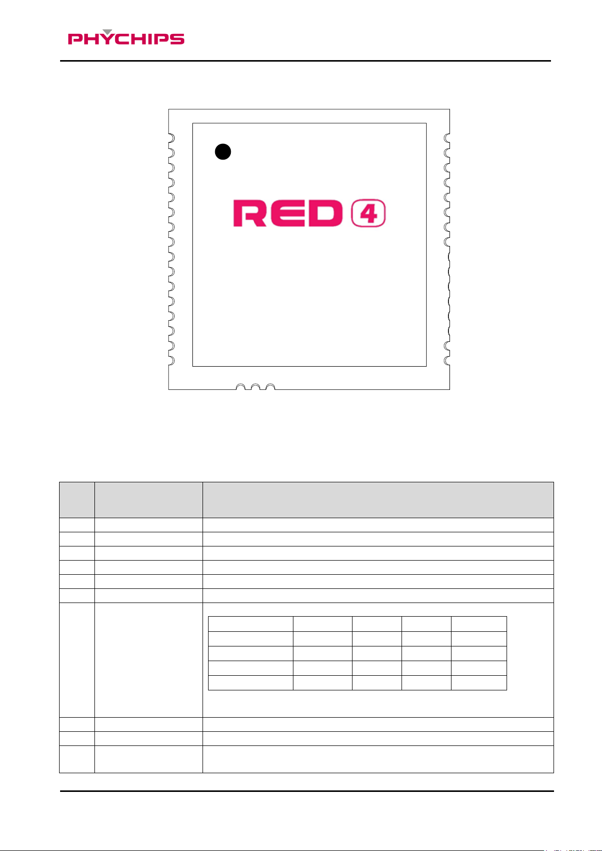
1 Pin Description
Figure 1 Pin Description
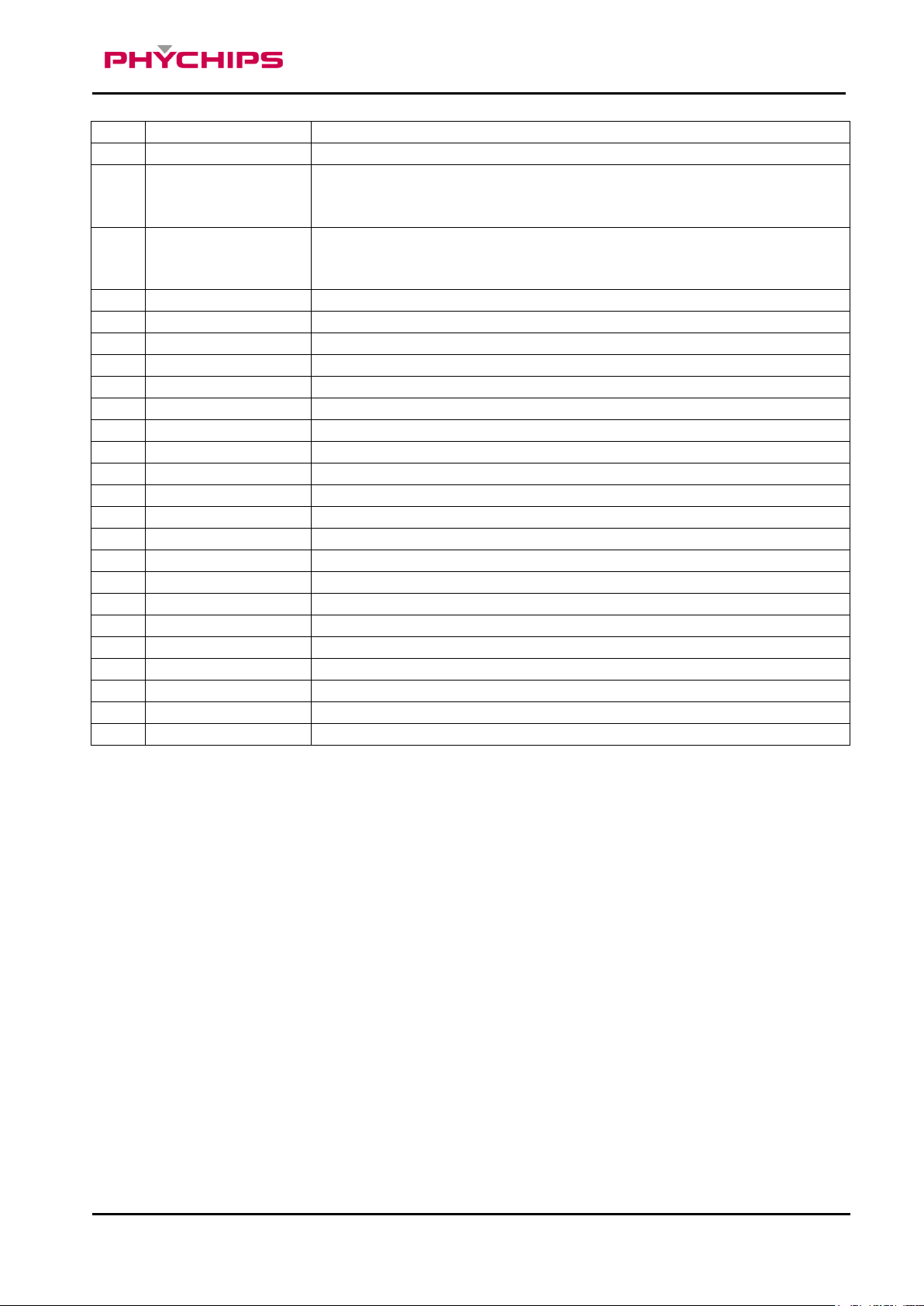
1.1 RED4 Pin Description
Page 4
31 March 2017
4 of 13
RED4 User’s Manuals - Preliminary Version
11
P16
Quasi-bi directional I/O port or External Interrupt 4
12
P17
Quasi-bi directional I/O port or External Interrupt 5
13
P12_SCL
Quasi-bi directional I/O port I2C Clock
The pull-up resistor is always switched on.
Reserved Address : 0x70, 0x71
14
P11_SDA
Quasi-bidirectional I/O port I2C Data In / Out
The pull-up resistor is always switched on.
Reserved Address : 0x70, 0x71
15
GND
Ground
16
GND
Ground
17
GND
Ground
18
RF IO
Rx Input / Tx Output
19
GND
Ground
20
VCC36P
DC Power for Power Amp
21
VCC36P
DC Power for Power Amp
22
GND
Ground
23
GND
Ground
24
GND
Ground
25
GND
Ground
26
GND
Ground
27
GND
Ground
28
SWDIO
Serial Wire Debug data in out
29
SWCLK
Serial Wire Debug Clock
30
RESETb
Reader SOC Reset signal 0: reset
31
NC
Not Connection
32
NC
Not Connection
33
NC
Not Connection
34
P01_TXD0
Quasi-bi directional I/O port or UART0 Output
35
P00_RXD0
Quasi-bi directional I/O port or UART0 Input
Page 5
31 March 2017
5 of 13
RED4 User’s Manuals - Preliminary Version
Host MCU
TXDx
RXDx
GND
TXD
RXD
GND
REDx
USB Tranceiver
TXDx
RXDx
GND
RXOUT
TXIN
GND
D+
VBUS
GND
USB
D-
D+
VBUS
GND
D-
REDx
2 Operation Method
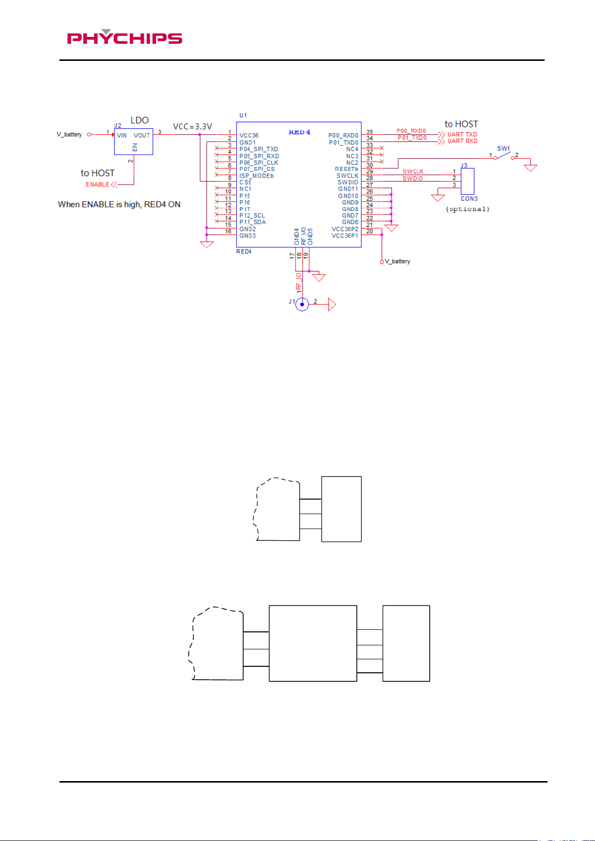
Figure 2 Application Circuit
2.1 Power Supply
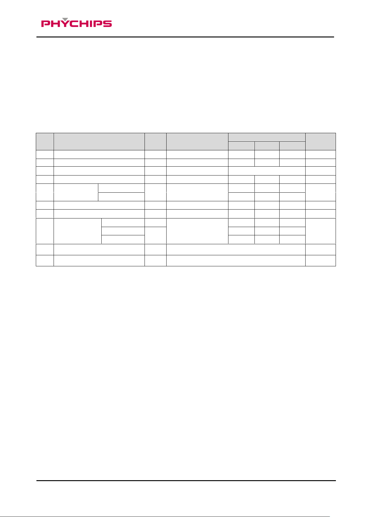
DC power to operate RED4 is separated by 2 kinds. VCC36 is to supply for PR9200 which power range is 3.3
to 3.6 volts, VCC36P is to supply for power amp which power range is 3.3 to 4.2 volts. Total current consumption
of RED4 is typically 450mA at 25dBm output power.
2.2 UART
The serial interface is assigned with two wires. RXD0, which pin is assigned to pin 35, is for receiving command
from host and TXD0, which pin is assigned to pin 34, is for transmitting response to host. Pin connection is
shown as below figure.
Following configuration is used for interfacing to USB transceiver.
2.3 RF In/Out
RF I/O which assigned to Pin 18 is optimized with 50ohm impedance.
Figure 3 Host MCU Connection
Figure 4 USB transceiver Connection
Page 6
31 March 2017
6 of 13
RED4 User’s Manuals - Preliminary Version
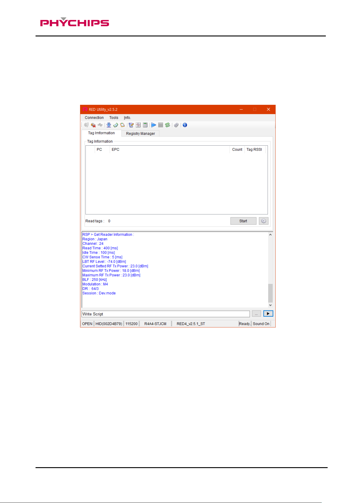
2.4 GUI Control
The RED Utility helps the user to start working with RED DK RFID reader quickly.
Follow below steps to run GUI.
Windows Start button Program Menu RED Utility_vX.X.X
Figure 5 RED Utility_vX.X.X
Page 7
31 March 2017
7 of 13
RED4 User’s Manuals - Preliminary Version
2.4.1 Mode Change
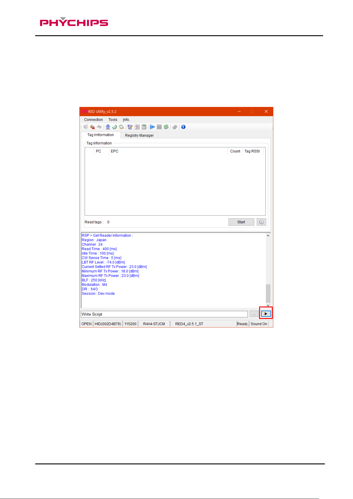
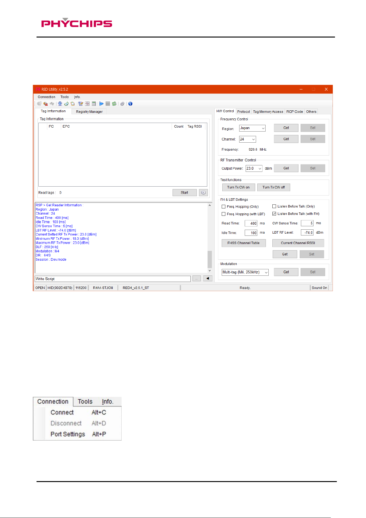
RED Utility provides two view modes. User can select view mode depending on purpose of use between
Basic View Mode and Extended View Mode.
To change View Mode, click the extension button marked red in Figure 6 above.
Figure 6 Basic View Mode
Page 8
31 March 2017
8 of 13
RED4 User’s Manuals - Preliminary Version
Figure 7 Extended View Mode
Always use Extended View Mode for measurement.
2.4.2 RED4 Connection
If hardware connection is valid, RED utility connect module REDx automatically.
If utility cannot connect hardware, please follow below step
Click “Connection->Connect” to connect to REDx-DK through USB-to-UART at main window
GUI will find the Device and synchronize parameters with REDx module automatically. If the GUI cannot find
the device automatically, Click “Connection->Port Setting” and select other Device. Default Baud rate is 115200
bit/s.
If the Device connected successfully, status bar will display “OPEN” state and device number and so on.
Page 9
31 March 2017
9 of 13
RED4 User’s Manuals - Preliminary Version
2.4.3 Hardware Control
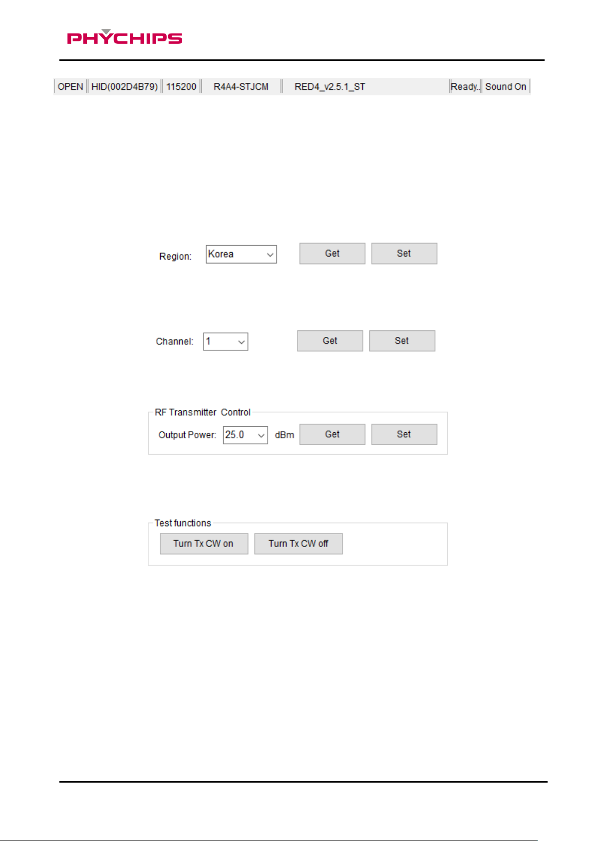
Click ‘H/W Control Tab.’ To control hardware.
2.4.3.1 Band(Region) Setting
To select operating band, band setting should be required. Select band in combo box and click Set button to
set operating band in group box ‘Frequency Control.’
2.4.3.2 Power Class Setting
Some countries classify channel number by power class. Click Get button and choose required power class.
And then click Set button to set finally.
.
2.4.3.3 Output Power setting
To set RED output power, select the Output Power combo box and click Set button.
2.4.3.4 CW (Continuous Wave) setting
It is only used for hardware debugging.
To set CW on, click Turn Tx CW on button. To set CW off, click Tx CW off button.
Page 10
31 March 2017
10 of 13
RED4 User’s Manuals - Preliminary Version
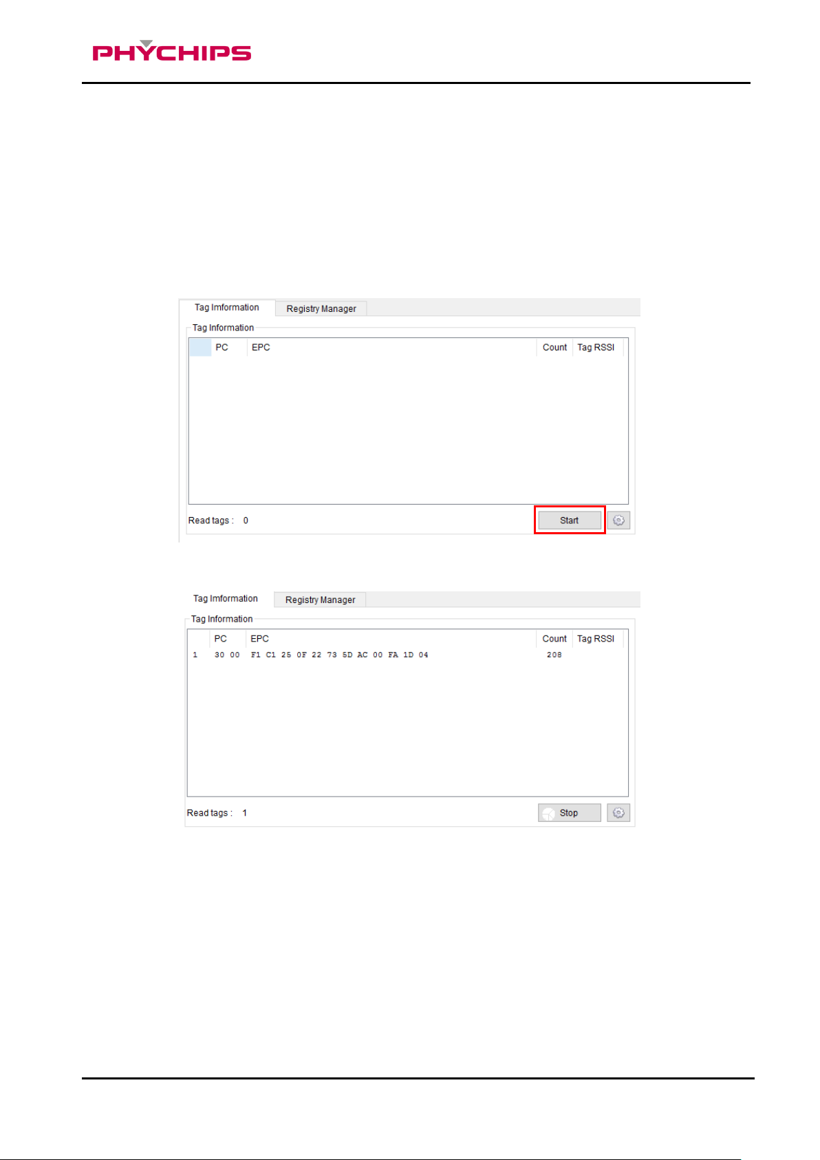
2.4.4 Tag Inventory Procedure
Click Start button in Tag Information Tab to read UHF RFID tag with RED Utility.
Click Start button and Tag’s EPC information is displayed.
Page 11
31 March 2017
11 of 13
RED4 User’s Manuals - Preliminary Version
No.
Item
Unit
Test Condition
Specification
Remark
min
Typ.
max
1
Frequency Range
MHz
917.1
926.9
2
Tx Power
dBm
25
3
Spurious
dBm
US (FCC 15C)
4
Impedance
Ω
50 RF I/O
5
DC Power
VCC36P
V
3.3
3.6
4.2
VCC36
3.3 3.6
6
Operating Temperature
°C -20 70 7
Operating Humidity
% 0 90
8
Current
Power Down
uA
Active current is
measured at 25dBm
with 50ohm load
20
Idle
mA
20
Active
450
9
Size
mm
24.0 * 24.0 * 3.0
10
Weight
g 3
•Device Name(Model Name) : RED4
•Certification No.:
•Name of Grantee: PHYCHIPS Inc.
•Production year, month, date:
•Manufacturer/Country:
3 Specification
Page 12

31 March 2017
12 of 13
RED4 User’s Manuals - Preliminary Version
FCC Information to User
This equipment has been tested and found to comply with the limits for a digital device, pursuant to part 15 of
the FCC Rules.
These limits are designed to provide reasonable protection against harmful interference when the equipment
is operated in a commercial environment.
This equipment generates, uses, and can radiate radio frequency energy and, if not installed and used in
accordance with the instruction manual, may cause harmful interference to radio communications.
Operation of this equipment in a residential area is likely to cause harmful interference in which case the user
will be required to correct the interference at his own expense.
This device complies with Part 15 of FCC Rules. Operation is subject to the following two conditions:
(1) the device may not cause interference, and
(2) the device must accept any interference, including interference that may cause undesired operation of this
device.
Caution : Any changes or modifications in construction of this device which are not expressly approved by the
party responsible for compliance could void the user's authority to operate the equipment
This device generates, uses and can radiate radio frequency energy and, if not installed and used in accordance
with the instructions, may cause harmful interference to radio communications. However, there is no guarantee
that interference will not occur in a particular installation. If this equipment does cause harmful interference to
radio or television reception, which can be determined by turning the equipment off and on, the user is
encouraged to try to correct the interference by one or more of the following measures:
– Reorient or relocate the receiving antenna.
– Increase the separation between the equipment and receiver.
– Connect the equipment into an outlet on a circuit different from that to which the receiver is connected.
– Consult the dealer or an experienced radio/TV technical for help.
End Product Labeling
The module is labeled with its own FCC. If the FCC ID is not visible when the module is installed inside
another device, then the outside of the device into which the module is installed must also display a label
referring to the enclosed module. In that case, the final end product must be labeled in a visible area with the
following:
“
Contains FCC ID: Y3D-RED4”
OEM Responsibilities to comply with FCC and Industry Canada Regulations
The module has been certified for integration into products only by OEM integrators under the following
condition:
- The antenna(s) must be installed such that a minimum separation distance of at least 20 cm
ismaintained between the radiator (antenna) and all persons at all times.
- The module is limited to installation in mobile or fixed applications.
- The transmitter module must not be co-located or operating in conjunction with any other antenna
ortransmitter except in accordance with FCC multi-transmitter product procedures.
- Separate approval will be required for all other operating configurations, including
portableconfigurations with respect to Part 2.1093 and different antenna configurations other than
suppliedantennas.
As long as the two condition above is met, further transmitter testing will not be required. However, the OEM
integrator is still responsible for testing their end-product for any additional compliance requirements required
with this module installed (for example, digital device emissions, PC peripheral requirements, etc.).
Page 13
31 March 2017
13 of 13
RED4 User’s Manuals - Preliminary Version
Peak Gain
Part Name
ANT1
2.79 dBi
KSA – 921A6010B100B
ANT2
0.99 dBi
KSA – 921A4010B100B
ANT3
-0.34 dBi
KSA –SP921MS25P20P4B
In the event that these conditions cannot be met, then the FCC authorizations are no longer considered valid
and the FCC ID cannot be used on the final product. In these circumstances, the OEM integrator will be
responsible for re-evaluating the end product including this module and obtaining separate FCC
authorizations.
- This device is intended only for OEM integrators
- For OEM integration only – device cannot be sold to general public.
- Manual Information to the End User
The OEM integrator has to be aware not to provide information to the end user regarding how
to install or remove this RF module in the user’s manual of the end product which integrates
this module.
This module has to install the input the 3.3V, cause there is no regulator in the device.
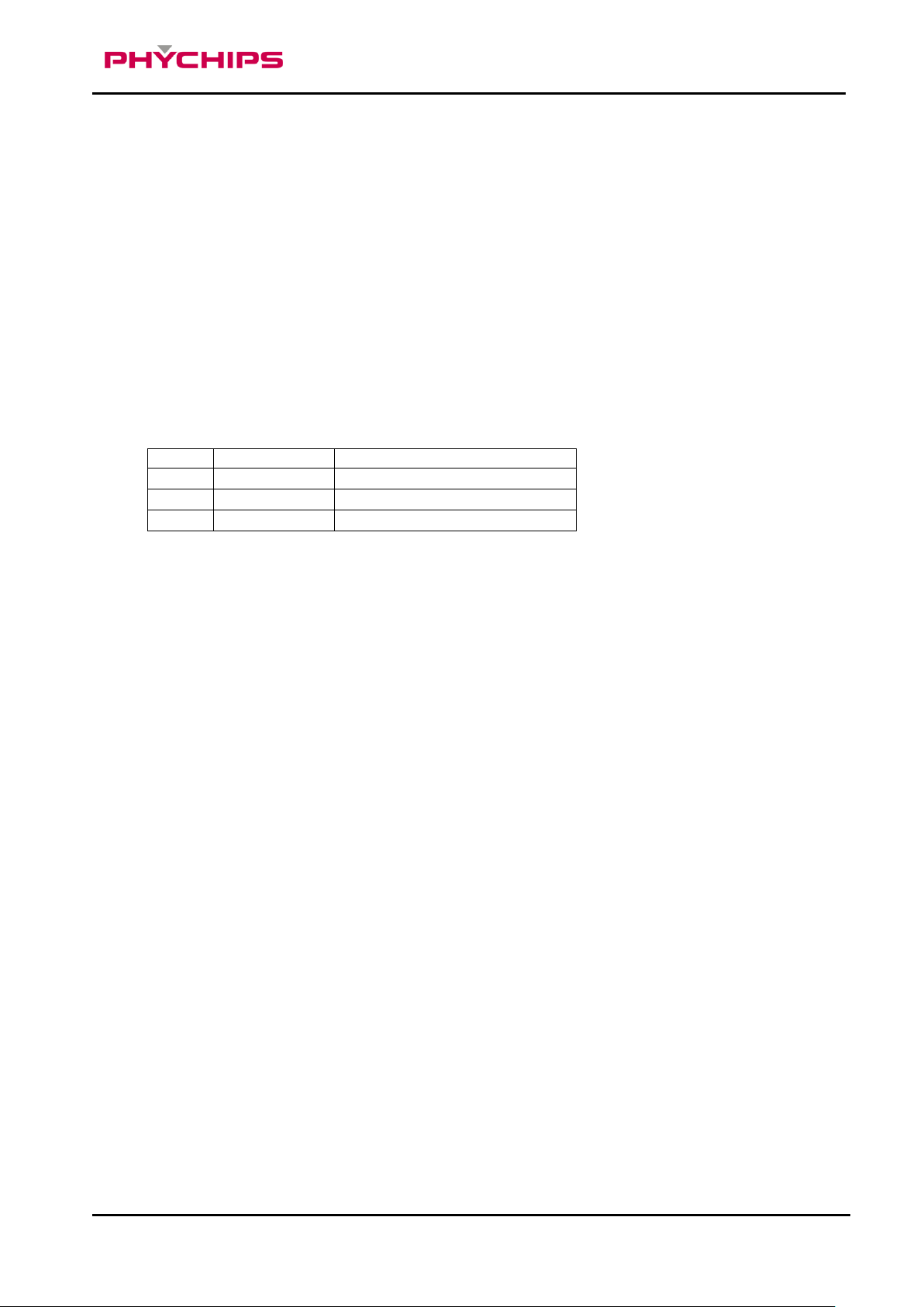
This device may only operate using an antenna of a type and maximum (or lesser) gain approved by
Phychips. Antenna types not included in the list, having a gain greater than the maximum gain indicated
for that type, are strictly prohibited for use with this transmitter.
Note
-
 Loading...