

Philips (Now NXP) BZX99-C10, BZX99-C11, BZX99-C12, BZX99-C13, BZX99-C15 Schematic [ru]
...
DISCRETE SEMICONDUCTORS
DATA SH EET
ook, halfpage
M3D088
BZX99 series
Voltage regulator diodes
Product specification
Supersedes data of 1999 May 31
1999 Oct 20
Philips Semiconductors Product specification
Voltage regulator diodes BZX99 series
FEATURES
• Total power dissipation: max. 300 mW
• Tolerance: ±5%
• Working voltage range: nom. 2.4 to 15 V (E24 range)
• Improved Iz/Vz characteristics at low currents
(Iz=50µA). This results in a noise free and sharp
breakdown knee.
APPLICATIONS
• General regulation functions, where low noise at low
currents is required
• Low-power consumption applications (e.g. hand-held
applications).
DESCRIPTION
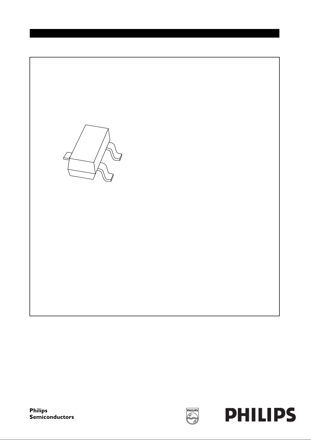
Low-power low noise voltage regulator diodes in small
SOT23 plastic SMD packages.
The diodes are available in the normalized E24 ±5%
tolerance range. The series consists of 20 types with
nominal working voltages from 2.4 to 15 V.
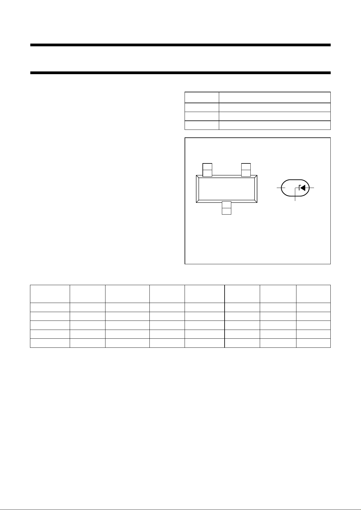
PINNING
PIN DESCRIPTION
1 anode
2 not connected
3 cathode
handbook, halfpage
21
2
n.c.
3
Top view
Fig.1 Simplified outline (SOT23) and symbol.
1
3
MAM243
MARKING
TYPE
NUMBER
MARKING
CODE
TYPE
NUMBER
MARKING
CODE
TYPE
NUMBER
MARKING
CODE
TYPE
NUMBER
MARKING
CODE
BZX99-C2V4 XL BZX99-C3V9 XS BZX99-C6V2 XD BZX99-C10 XX
BZX99-C2V7 XM BZX99-C4V3 XT BZX99-C6V8 XE BZX99-C11 XY
BZX99-C3V0 XN BZX99-C4V7 XA BZX99-C7V5 XU BZX99-C12 XZ
BZX99-C3V3 XP BZX99-C5V1 XB BZX99-C8V2 XV BZX99-C13 X2
BZX99-C3V6 XR BZX99-C5V6 XC BZX99-C9V1 XW BZX99-C15 X3
1999 Oct 20 2
Philips Semiconductors Product specification
Voltage regulator diodes BZX99 series
LIMITING VALUES
In accordance with the Absolute Maximum Rating System (IEC 134).
SYMBOL PARAMETER CONDITIONS MIN. MAX. UNIT
I
F
I
ZSM
P
tot
T
stg
T
j
Note
1. Device mounted on an FR4 printed-circuit board.
ELECTRICAL CHARACTERISTICS
Total BZX99-C series
Tj=25°C unless otherwise specified.
continuous forward current − 300 mA
non-repetitive peak reverse current tp= 100 µs; square wave;
T
=25°C prior to surge
amb
total power dissipation T
=25°C; note 1 − 300 mW
amb
see Table 1
storage temperature −65 +150 °C
junction temperature − 150 °C
SYMBOL PARAMETER CONDITIONS MAX. UNIT
V
F
I
R
forward voltage IF= 10 mA; see Fig.4 0.9 V
= 100 mA; see Fig.4 1 V
I
F
reverse current
BZX99-C2V4 V
BZX99-C2V7 V
BZX99-C3V0 V
BZX99-C3V3 V
BZX99-C3V6 V
BZX99-C3V9 V
BZX99-C4V3 V
BZX99-C4V7 V
BZX99-C5V1 V
BZX99-C5V6 V
BZX99-C6V2 V
BZX99-C6V8 V
BZX99-C7V5 V
BZX99-C8V2 V
BZX99-C9V1 V
BZX99-C10 V
BZX99-C11 V
BZX99-C12 V
BZX99-C13 V
BZX99-C15 V
=1V 0.2 µA
R
= 1 V 0.05 µA
R
= 1 V 0.02 µA
R
=2V 2 µA
R
=2V 1 µA
R
=2V 0.5 µA
R
=2V 0.1 µA
R
=3V 2 µA
R
=3V 1 µA
R
=4V 1 µA
R
=5V 0.1 µA
R
= 5 V 0.01 µA
R
=5V 0.1 µA
R
=6V 0.2 µA
R
=7V 0.1 µA
R
=7V 0.1 µA
R
= 8 V 0.05 µA
R
= 9 V 0.05 µA
R
= 10 V 0.05 µA
R
= 10.5 V 0.01 µA
R
1999 Oct 20 3
 Loading...