Philips (Now NXP) BSS123 Schematic [ru]

Philips Semiconductors Product specification
N-channel TrenchMOS transistor BSS123
Logic level FET
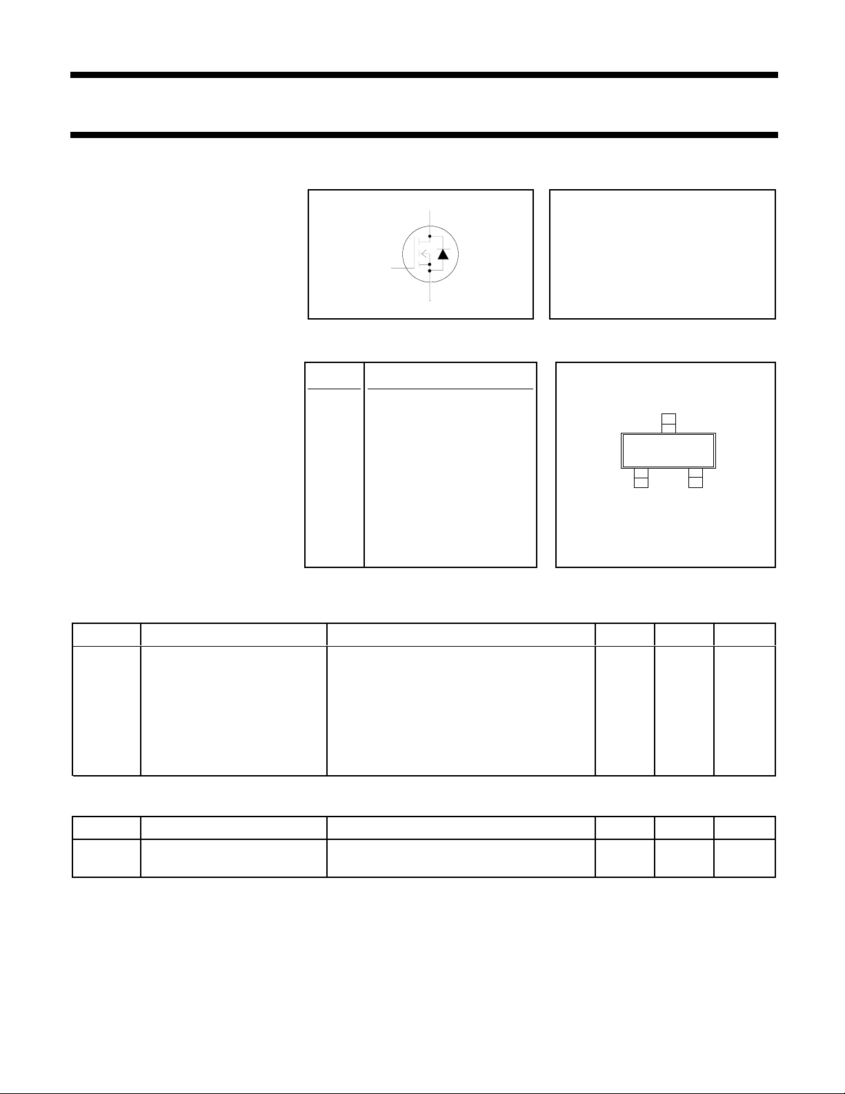
FEATURES SYMBOL QUICK REFERENCE DATA
• ’Trench’ technology
d
• Extremely fast switching V
• Logic level compatible
• Subminiature surface mounting I
package
g
R
DS(ON)
s
GENERAL DESCRIPTION PINNING SOT23
N-channel enhancement mode PIN DESCRIPTION
field-effect transistor in a plastic
envelope using ’trench’ 1 gate
technology.
2 source
Applications:-
• Relay driver 3 drain
• High-speed line driver
• Telephone ringer
The BSS123 is supplied in the
SOT23 subminiature surface mounting package.
LIMITING VALUES
Limiting values in accordance with the Absolute Maximum System (IEC 134)
= 100 V
DSS
= 150 mA
D
≤ 6 Ω (VGS = 10 V)
3
Top view
1
2
SYMBOL PARAMETER CONDITIONS MIN. MAX. UNIT
V
DSS
V
DGR
V
GS
I
D
I
DM
P
D
Tj, T
Drain-source voltage Tj = 25 ˚C to 150˚C - 100 V
Drain-gate voltage Tj = 25 ˚C to 150˚C; RGS = 20 kΩ - 100 V
Gate-source voltage - ± 20 V
Continuous drain current Ta = 25 ˚C - 150 mA
Pulsed drain current Ta = 25 ˚C - 600 mA
Total power dissipation Ta = 25 ˚C - 0.25 W
Operating junction and - 55 150 ˚C
stg
storage temperature
THERMAL RESISTANCES
SYMBOL PARAMETER CONDITIONS TYP. MAX. UNIT
R
th j-a
Thermal resistance junction surface mounted on FR4 board 500 - K/W
to ambient
August 2000 1 Rev 1.000

Philips Semiconductors Product specification
N-channel TrenchMOS transistor BSS123
Logic level FET
ELECTRICAL CHARACTERISTICS
Tj= 25˚C unless otherwise specified
SYMBOL PARAMETER CONDITIONS MIN. TYP. MAX. UNIT
V
(BR)DSS
V
GS(TO)
R
DS(ON)
g
fs
I
DSS
I
GSS
t
on
t
off
C
iss
C
oss
C
rss
Drain-source breakdown VGS = 0 V; ID = 10 µA 100 130 - V
voltage
Gate threshold voltage VDS = VGS; ID = 1 mA 1 2 2.8 V
Drain-source on-state VGS = 10 V; ID = 120 mA - 3.5 6 Ω
resistance
Forward transconductance VDS = 25 V; ID = 120 mA - 350 - mS
Zero gate voltage drain VDS = 60 V; VGS = 0 V - 10 100 nA
current
Gate source leakage current VGS = ±20 V; VDS = 0 V - 10 100 nA
Turn-on time VDD = 50 V; RD = 250 Ω; VGS = 10 V; - 3 10 ns
RG = 50 Ω; Resistive load
Turn-off time - 12 20 ns
Input capacitance VGS = 0 V; VDS = 25 V; f = 1 MHz - 23 40 pF
Output capacitance - 6 25 pF
Feedback capacitance - 4 10 pF
August 2000 2 Rev 1.000
 Loading...