

Philips (Now NXP) BSR17A Schematic [ru]
DISCRETE SEMICONDUCTORS
DATA SH EET
ook, halfpage
M3D088
BSR17A
NPN switching transistor
Product specification
Supersedes data of 1997 Jun 02
2004 Mar 24
Philips Semiconductors Product specification
NPN switching transistor BSR17A
FEATURES
• Low current (max. 100 mA)
• Low voltage (max. 40 V).
APPLICATIONS
• Switching and linear amplification.
DESCRIPTION
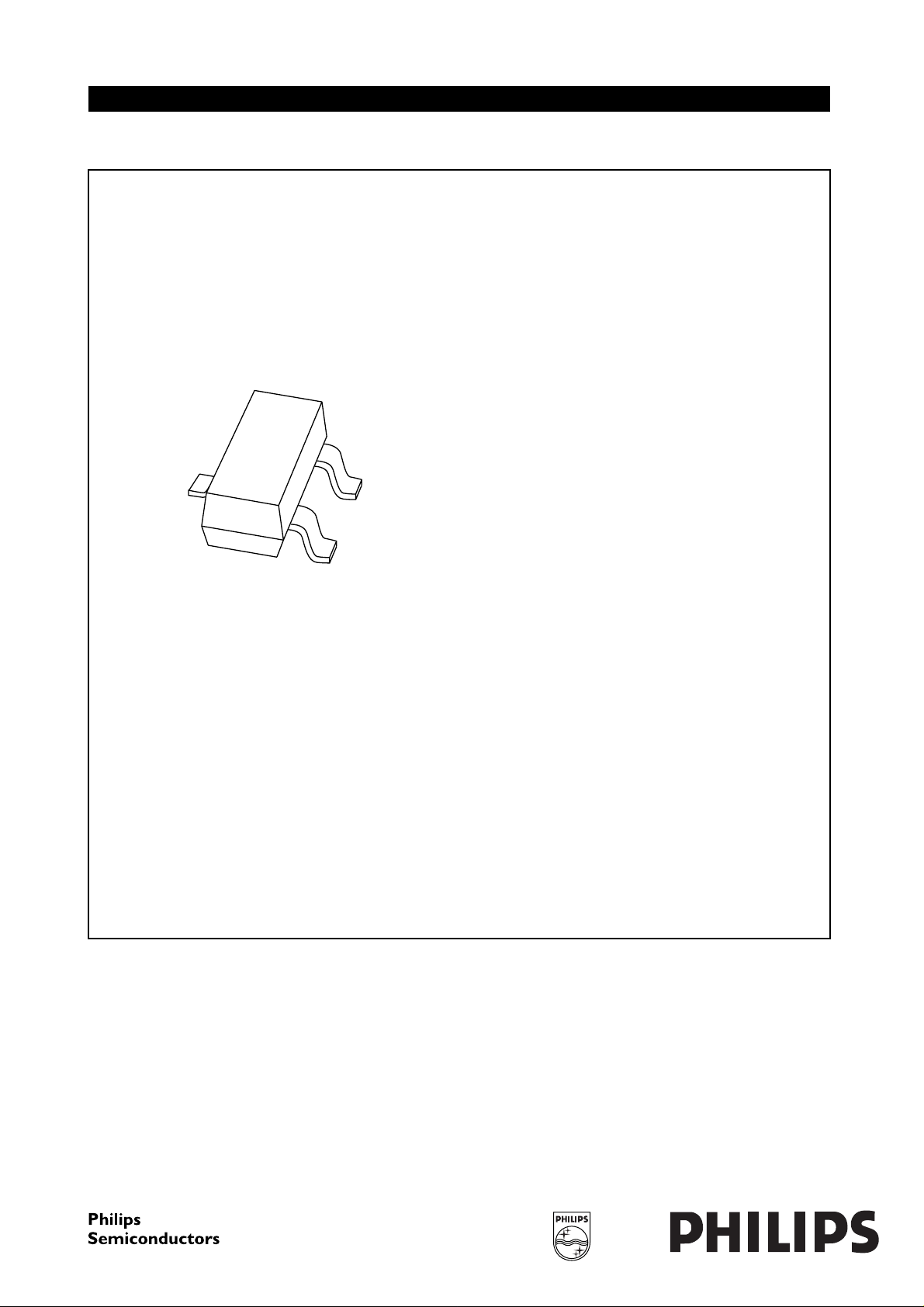
NPN switching transistor in a SOT23 plastic package.
PNP complement: BSR18A.
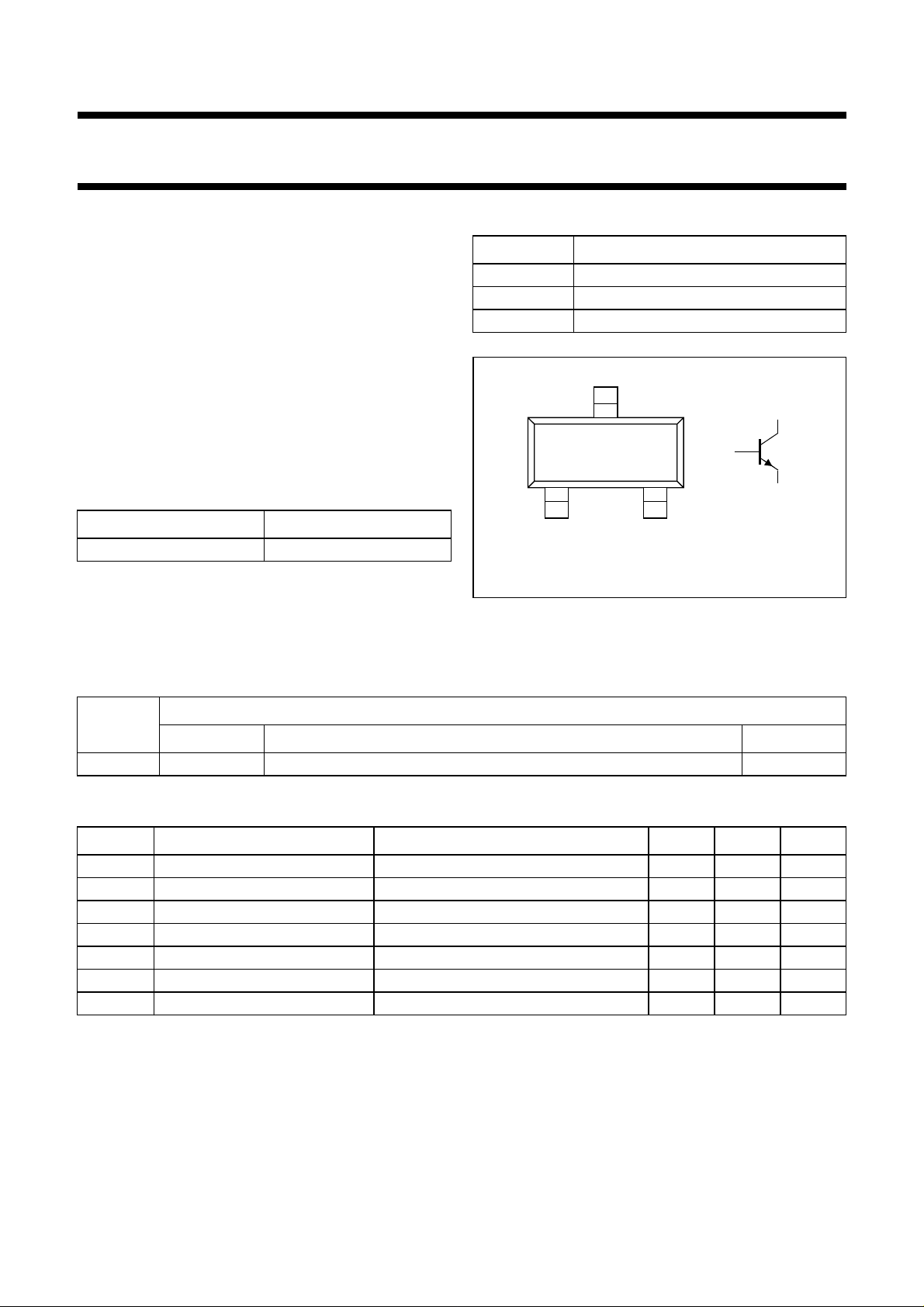
MARKING
TYPE NUMBER MARKING CODE
(1)
BSR17A 54* or U92
Note
1. * = p: Made in Hong Kong.
* = t: Made in Malaysia.
* = W: Made in China.
PINNING
PIN DESCRIPTION
1 base
2 emitter
3 collector
handbook, halfpage
Top view
3
21
MAM255
Fig.1 Simplified outline (SOT23) and symbol.
3
1
2
ORDERING INFORMATION
TYPE
NUMBER
NAME DESCRIPTION VERSION
PACKAGE
BSR17A − plastic surface mounted package; 3 leads SOT23
QUICK REFERENCE DATA
SYMBOL PARAMETER CONDITIONS MIN. MAX. UNIT
V
V
I
P
h
f
t
CBO
CEO
C
tot
FE
T
off
collector-base voltage open emitter − 60 V
collector-emitter voltage open base − 40 V
collector current (DC) − 100 mA
total power dissipation T
≤ 25 °C − 250 mW
amb
DC current gain IC= 10 mA; VCE= 1 V 100 300
transition frequency IC= 10 mA; VCE= 20 V; f = 100 MHz 300 − MHz
turn-off time I
= 10 mA; I
Con
Bon
= 1 mA; I
= −1mA − 240 ns
Boff
2004 Mar 24 2
Philips Semiconductors Product specification
NPN switching transistor BSR17A
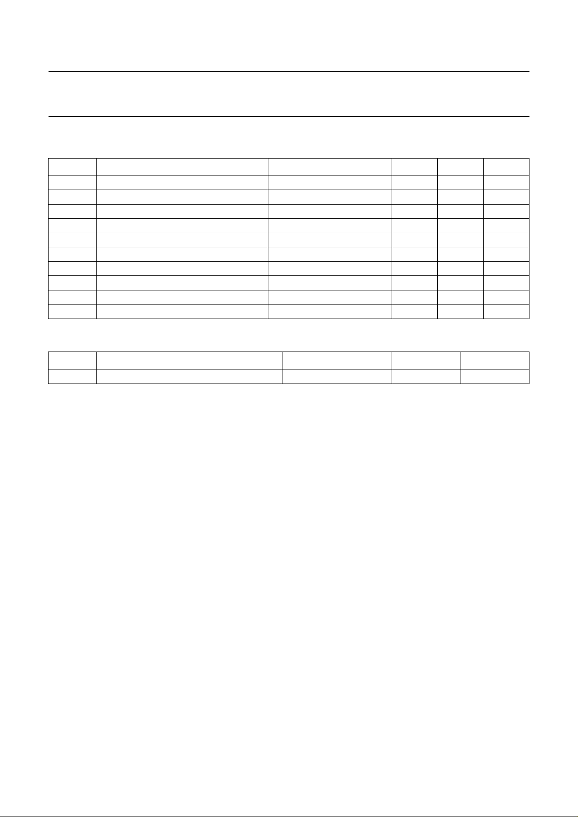
LIMITING VALUES
In accordance with the Absolute Maximum Rating System (IEC 60134).
SYMBOL PARAMETER CONDITIONS MIN. MAX. UNIT
V
CBO
V
CEO
V
EBO
I
C
I
CM
I
BM
P
tot
T
stg
T
j
T
amb
THERMAL CHARACTERISTICS
collector-base voltage open emitter − 60 V
collector-emitter voltage open base − 40 V
emitter-base voltage open collector − 6V
collector current (DC) − 100 mA
peak collector current − 200 mA
peak base current − 100 mA
total power dissipation T
≤ 25 °C − 250 mW
amb
storage temperature −65 +150 °C
junction temperature − 150 °C
operating ambient temperature −65 +150 °C
SYMBOL PARAMETER CONDITIONS VALUE UNIT
R
th(j-a)
thermal resistance from junction to ambient note 1 500 K/W
Note
1. Transistor mounted on an FR4 printed-circuit board.
2004 Mar 24 3
 Loading...