DISCRETE SEMICONDUCTORS
DATA SHEET
ook, halfpage
MBD128
BGM1011
MMIC wideband amplifier
Preliminary specification 2002 Jan 14

Philips Semiconductors Preliminary specification
MMIC wideband amplifier BGM1011
FEATURES
• Internally matched to 50 Ω
• Very high gain (up to 37 dB at 2 Ghz)
• Sloped gain curve for optimal performance
with output into lossy cable
• 14 dBm saturated output power at 1 GHz
• High linearity (23 dBm IP3
at 1 GHz)
(out)
• 40 dB isolation
APPLICATIONS
• LNB IF amplifiers
• Cable systems
• General purpose.
DESCRIPTION
Silicon Monolithic Microwave Integrated Circuit (MMIC)
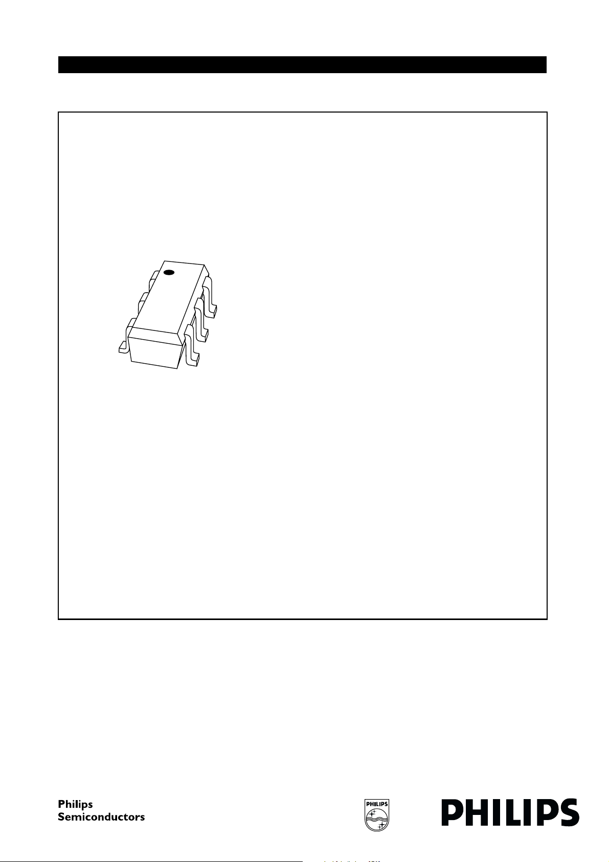
wideband amplifier with internal matching circuit in a 6-pin
SOT363 SMD plastic package.
PINNING
PIN DESCRIPTION
1V
S
2, 5 GND2
3 RF out
4GND1
6RF in
56
4
63
132
Top view
Marking code: C1-.
MAM455
Fig.1 Simplified outline (SOT363) and symbol.
1
2, 54
QUICK REFERENCE DATA
SYMBOL PARAMETER CONDITIONS TYP. MAX. UNIT
V
S
I
S
2
|s
|
21
DC supply voltage 5 6 V
DC supply current 25.5 − mA
insertion power gain f = 1 GHz 30 − dB
NF noise figure f = 1 GHz 4.7 − dB
P
L(sat)
saturated load power f = 1 GHz 13.8 − dBm
LIMITING VALUES
In accordance with the Absolute Maximum Rating System (IEC 60134)
SYMBOL PARAMETER CONDITIONS MIN. MAX. UNIT
V
S
I
S
P
tot
T
stg
T
j
P
D
DC supply voltage RF input AC coupled − 6V
supply current − 35 mA
total power dissipation Ts≤ 90 °C − 200 mW
storage temperature −65 +150 °C
operating junction temperature − 150 °C
maximum drive power − 0dBm
CAUTION
This product is supplied in anti-static packing to prevent damage caused by electrostatic discharge during transport
and handling. For further information, refer to Philips specs.: SNW-EQ-608, SNW-FQ-302A and SNW-FQ-302B.
2002 Jan 14 2

Philips Semiconductors Preliminary specification
MMIC wideband amplifier BGM1011
THERMAL RESISTANCE
SYMBOL PARAMETER CONDITIONS VALUE UNIT
R
th j-s
CHARACTERISTICS
V
=5V; IS=25.5mA; Tj=25°C unless otherwise specified.
S
SYMBOL PARAMETER CONDITIONS MIN. TYP. MAX. UNIT
I
S
2
|s
|
21
R
L IN
R
L OUT
NF noise figure f = 1 GHz − 4.7 − dB
BW bandwidth at |s
K stability factor f = 1 GHz − 1.8 −−
P
L(sat)
P
L 1 dB
IP3
(in)
IP3
(out)
thermal resistance from junction to solder point P
= 200 mW; Ts≤ 90 °C 300 K/W
tot
supply current 20 25.5 32 mA
insertion power gain f = 100 MHz − 25 − dB
f=1GHz − 30 − dB
f=1.8GHz − 35 − dB
f=2.2GHz − 37 − dB
f=2.6GHz − 32 − dB
f=3GHz − 28 − dB
return losses input f = 1 GHz − 11 − dB
f=2.2GHz − 8 − dB
return losses output f = 1 GHz − 18 − dB
f=2.2GHz − 12 − dB
f=2.2GHz − 4.6 − dB
|2−3 dB below flat gain at 1 GHz − 2.9 − GHz
21
f=2.2GHz − 0.9 −−
saturated load power f = 1 GHz − 13.8 − dBm
f=2.2GHz − 10.8 − dBm
load power at 1 dB gain compression; f = 1 GHz − 12.2 − dBm
at 1 dB gain compression; f = 2.2 GHz − 7.7 − dBm
input intercept point f = 1 GHz −−7 − dBm
f=2.2GHz −−20 − dBm
output intercept point f = 1 GHz − 23 − dBm
f=2.2GHz − 16 − dBm
2002 Jan 14 3

Philips Semiconductors Preliminary specification
MMIC wideband amplifier BGM1011
APPLICATION INFORMATION
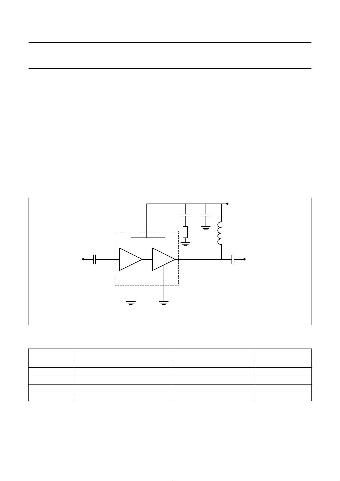
Figure 2 shows a typical application circuit for the BGM1011 MMIC. The device is internally matched to 50 Ω, and
therefore does not need any external matching. The value of the input and output DC blocking capacitors C1, C2 should
be not more than 100 pF for applications above 100 MHz. Their values can be used to fine tune the input and output
impedance. However, when the device is operated below 100 MHz, the capacitor value should be increased.
The nominal value of the RF choke, L1 is 100 nH. At frequencies below 100 MHz this value should be increased to
200 nH. At frequencies between 1 and 3 GHz a much lower value must be used (e.g. 18 nH) to improve return losses.
For optimal results, a good quality chip inductor such as the TDK MLG 1608 (0603), or a wire-wound SMD type should
be chosen.
Capacitor, C4 and resistor, R1 are added for optimal supply decoupling.
Both the RF choke, L1 and the 22 nF supply decoupling capacitor, C3 should be located as closely as possible to the
MMIC.
Separate paths must be used for the ground planes of the ground pins GND1, GND2, and these paths must be as short
as possible. When using vias, use multiple vias per pin in order to limit ground path inductance.
Vs
C
1
RF in
Fig.2 Typical application circuit
6 [In]
4 [GND1]
1 [Vs]
BGM1011
SOT363
3 [Out]
2,5 [GND2]
C
4
R
1
C
3
L
1
C
2
RF out
Fig.2 Typical application circuit
List of components used for the typical application; an amplifier for LNB IF output.
COMPONENT DESCRIPTION VALUE DIMENSIONS.
C1, C2 multilayer ceramic chip capacitor 100 pF 0603
C3 multilayer ceramic chip capacitor 22 nF 0603
C4 multilayer ceramic chip capacitor 5.6 pF 0603
R1 SMD resistor 10 Ω 0603
L1 SMD inductor 10 to 200 nH 0603
2002 Jan 14 4
 Loading...