

Philips (Now NXP) BFG403W Schematic [ru]
DISCRETE SEMICONDUCTORS
BFG403W
NPN 17 GHz wideband transistor
Product specification
Supersedes data of 1997 Oct 29
File under Discrete Semiconductors, SC14
1998 Mar 11
Philips Semiconductors Product specification
NPN 17 GHz wideband transistor BFG403W
FEATURES
• Low current
• Very high power gain
• Low noise figure
• High transition frequency
• Very low feedback capacitance.
APPLICATIONS
• Pager front ends
• RF front end
• Wideband applications, e.g. analog and digital cellular
telephones, cordless telephones (PHS, DECT, etc.)
• Radar detectors.
DESCRIPTION
NPN double polysilicon wideband transistor with buried
layer for low voltage applications in a plastic, 4-pin
dual-emitter SOT343R package.
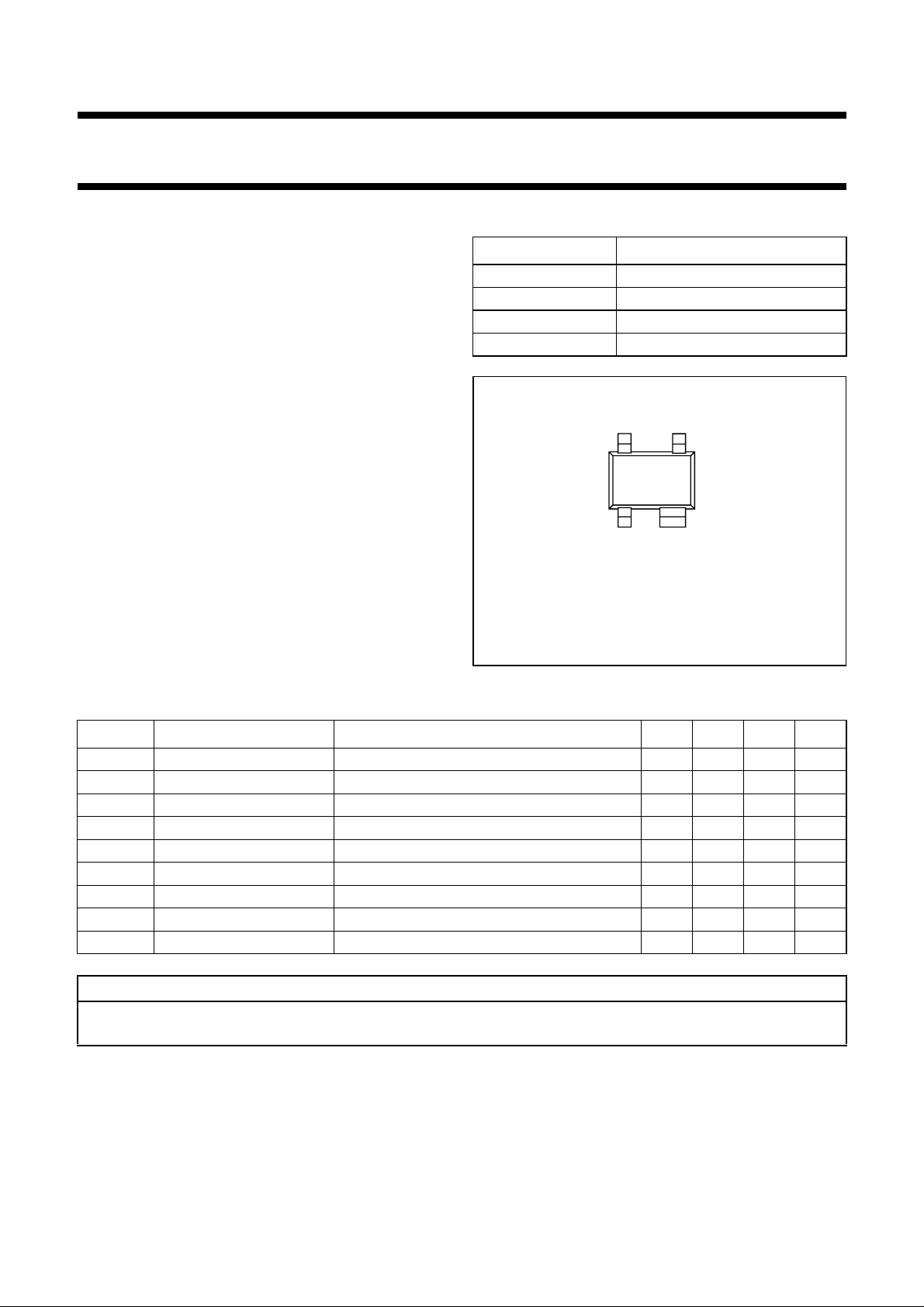
PINNING
PIN DESCRIPTION
handbook, halfpage
Marking code: P3.
1 emitter
2 base
3 emitter
4 collector
43
21
Top view
MSB842
Fig.1 Simplified outline SOT343R.
QUICK REFERENCE DATA
SYMBOL PARAMETER CONDITIONS MIN. TYP. MAX. UNIT
V
CBO
V
CEO
I
C
P
tot
h
FE
C
re
f
T
G
max
F noise figure I
collector-base voltage open emitter −−10 V
collector-emitter voltage open base −−4.5 V
collector current (DC) − 3 3.6 mA
total power dissipation Ts≤ 140 °C −−16 mW
DC current gain IC= 3 mA; VCE=2V; Tj=25°C 5080120
feedback capacitance IC= 0; VCB=2V; f=1MHz − 20 − fF
transition frequency IC= 3 mA; VCE= 2 V; f = 2 GHz; T
maximum power gain IC= 3 mA; VCE= 2 V; f = 2 GHz; T
= 1 mA; VCE= 2 V; f = 900 MHz; ΓS= Γ
C
=25°C − 17 − GHz
amb
=25°C − 22 − dB
amb
− 1 − dB
opt
CAUTION
This product is supplied in anti-static packing to prevent damage caused by electrostatic discharge during transport
and handling. For further information, refer to Philips specs.: SNW-EQ-608, SNW-FQ-302A and SNW-FQ-302B.
1998 Mar 11 2
Philips Semiconductors Product specification
NPN 17 GHz wideband transistor BFG403W
LIMITING VALUES
In accordance with the Absolute Maximum Rating System (IEC 134).
SYMBOL PARAMETER CONDITIONS MIN. MAX. UNIT
V
CBO
V
CEO
V
EBO
I
C
P
tot
T
stg
T
j
Note
1. T
s
THERMAL CHARACTERISTICS
collector-base voltage open emitter − 10 V
collector-emitter voltage open base − 4.5 V
emitter-base voltage open collector − 1V
collector current (DC) − 3.6 mA
total power dissipation Ts≤ 140 °C; note 1; see Fig.2 − 16 mW
storage temperature −65 +150 °C
operating junction temperature − 150 °C
is the temperature at the soldering point of the emitter pins.
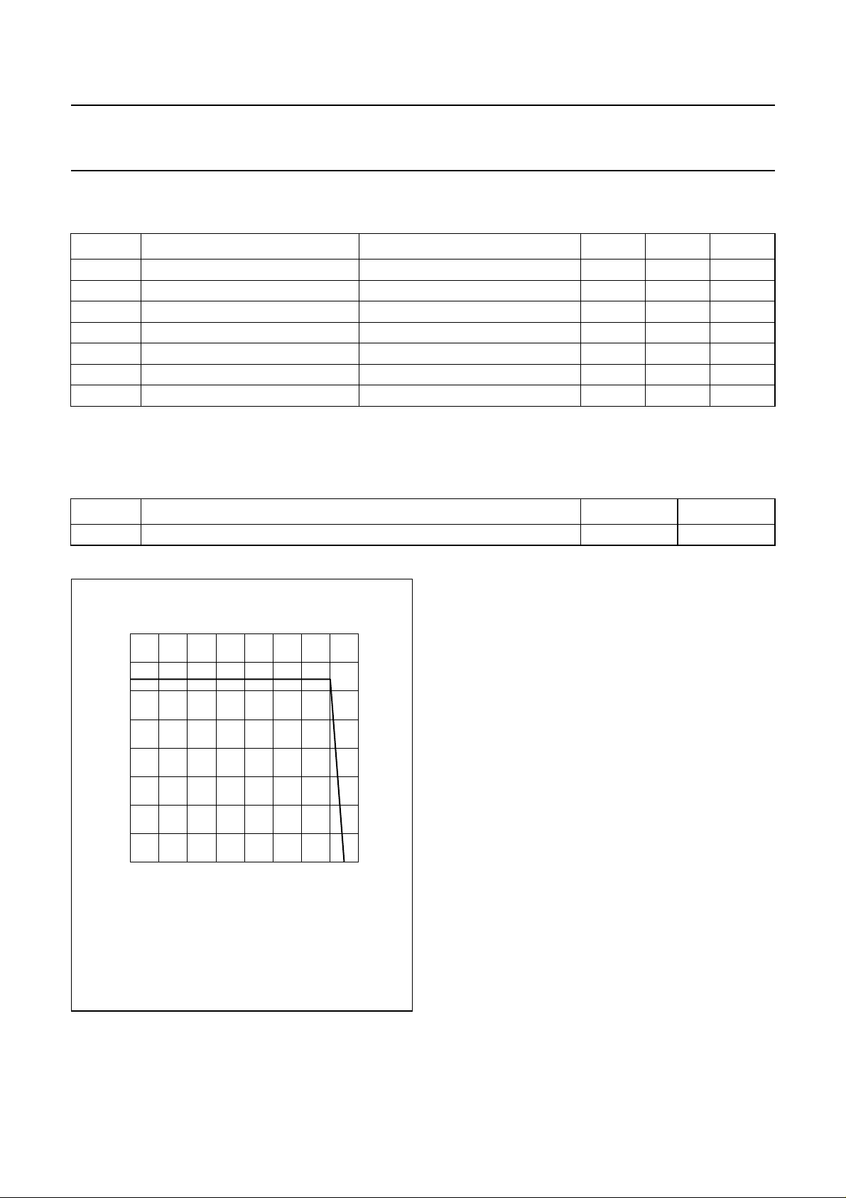
SYMBOL PARAMETER VALUE UNIT
R
th j-s
handbook, halfpage
P
(mW)
thermal resistance from junction to soldering point 820 K/W
20
tot
10
0
0 40 80 120 160
MGD957
Ts (°C)
Fig.2 Power derating curve.
1998 Mar 11 3
Philips Semiconductors Product specification
NPN 17 GHz wideband transistor BFG403W
CHARACTERISTICS
T
=25°C unless otherwise specified.
j
SYMBOL PARAMETER CONDITIONS MIN. TYP. MAX. UNIT
V
(BR)CBO
V
(BR)CEO
V
(BR)EBO
I
CBO
h
FE
C
c
C
e
C
re
f
T
G
max
S
21
F noise figure I
P
L1
ITO third order intercept point I
collector-base breakdown voltage IC= 2.5 µA; IE=0 10 −−V
collector-emitter breakdown voltage IC= 1 mA; IB= 0 4.5 −−V
emitter-base breakdown voltage IE= 2.5 µA; IC=0 1 −−V
collector-base leakage current IE= 0; VCB= 4.5 V −−15 nA
DC current gain IC= 3 mA; VCE= 2 V; see Fig.3 50 80 120
collector capacitance IE=ie= 0; VCB=2V; f=1MHz − 170 − fF
emitter capacitance IC=ic= 0; VEB= 0.5 V; f = 1 MHz − 315 − fF
feedback capacitance IC= 0; VCB= 2 V; f = 1 MHz;
− 20 − fF
see Fig.4
transition frequency IC= 3 mA; VCE= 2 V; f = 2 GHz;
T
=25°C; see Fig.5
amb
maximum power gain; note 1 IC= 0.5 mA; VCE= 1 V; f = 900 MHz;
T
=25°C; see Figs 6 and 8
amb
I
= 3 mA; VCE= 2 V; f = 2 GHz;
C
T
=25°C; see Figs 7 and 8
amb
insertion power gain I
2
output power at 1 dB gain
compression
= 0.5 mA; VCE= 1 V; f = 900 MHz;
C
T
=25°C; see Fig.8
amb
= 3 mA; VCE= 2 V; f = 2 GHz;
I
C
T
=25°C; see Fig.8
amb
= 1 mA; VCE= 2 V; f = 900 MHz;
C
ΓS= Γ
I
C
ΓS= Γ
; see Fig.13
opt
= 1 mA; VCE= 2 V; f = 2 GHz;
; see Fig.13
opt
IC= 1 mA; VCE= 1 V; f = 900 MHz;
ZS=Z
= 1 mA; VCE= 1 V; f = 900 MHz;
C
ZS=Z
S opt
S opt
; ZL=Z
; ZL=Z
L opt
L opt
; note 2
; note 2
− 17 − GHz
− 20 − dB
− 22 − dB
− 5 − dB
− 14 − dB
− 1 − dB
− 1.6 − dB
−−5−dBm
− 6 − dBm
Notes
1. G
is the maximum power gain, if K > 1. If K < 1 then G
max
2. ZS is optimized for noise; ZL is optimized for gain.
1998 Mar 11 4
= MSG; see Figs 6, 7 and 8.
max
 Loading...