

Philips (Now NXP) BCV64B Schematic [ru]
DISCRETE SEMICONDUCTORS
DATA SH EET
M3D071
BCV64B
PNP general purpose double
transistor
Product specification
Supersedes data of 1997 Mar 10
1999 May 21
Philips Semiconductors Product specification
PNP general purpose double transistor BCV64B
FEATURES
• Low current (max. 100 mA)
• Low voltage (max. 30 and 6 V).
APPLICATIONS
• General purpose switching and amplification
• For use in Schmitt-trigger applications.
DESCRIPTION
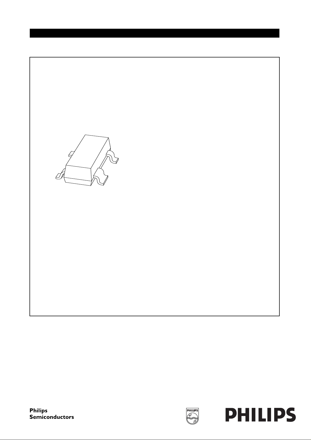
PNP double transistor in a SOT143B plastic package.
NPN complement: BCV63B.
MARKING
TYPE NUMBER MARKING CODE
BCV64B C96
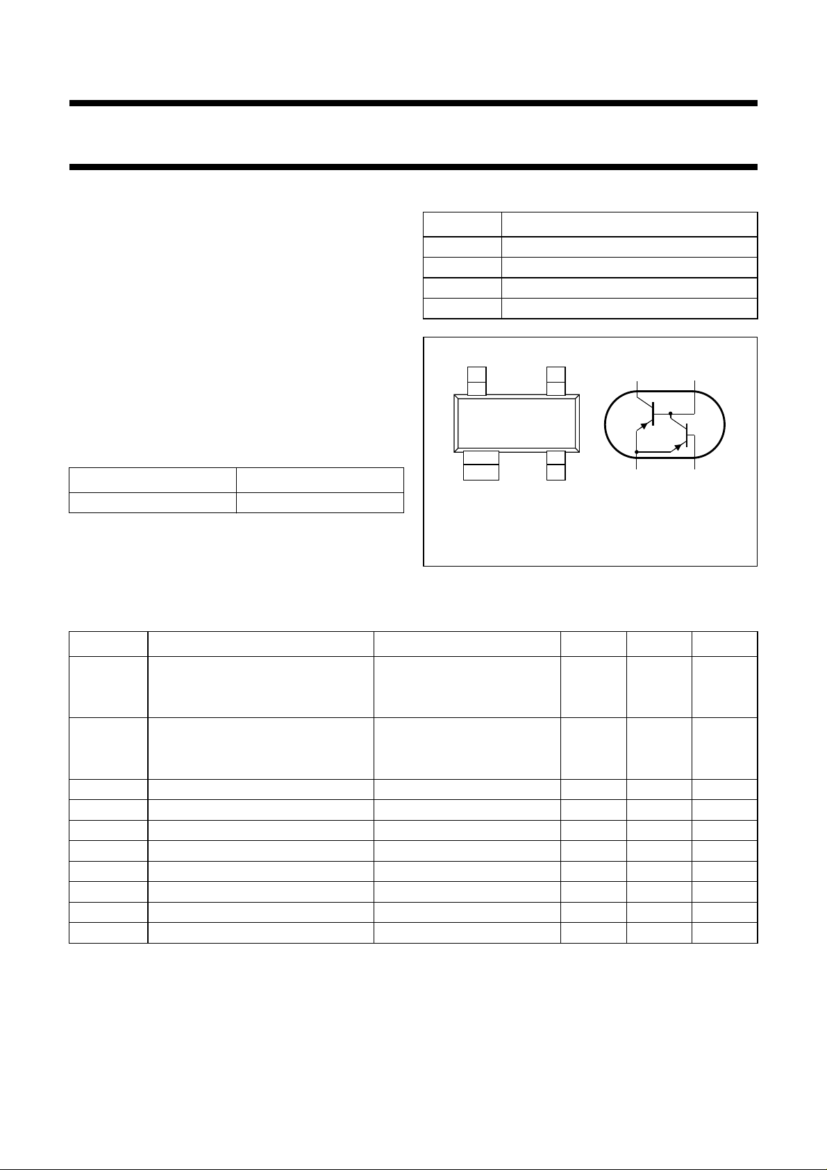
PINNING
PIN DESCRIPTION
1 collector TR2 and base TR1
2 collector TR1
3 emitter TR1 and TR2
4 base TR2
handbook, halfpage
4
Top view
3
12
21
TR1
TR2
34
MAM291
Fig.1 Simplified outline (SOT143B) and symbol.
LIMITING VALUES
In accordance with the Absolute Maximum Rating System (IEC 134).
SYMBOL PARAMETER CONDITIONS MIN. MAX. UNIT
V
CBO
collector-base voltage open emitter
TR1 −−30 V
TR2 −−6V
V
CEO
collector-emitter voltage open base
TR1 −−30 V
TR2 −−6V
V
EBO
I
C
I
CM
I
B
P
tot
T
stg
T
j
T
amb
emitter-base voltage open collector −−6V
collector current (DC) −−100 mA
peak collector current −−200 mA
base current (DC) −−100 mA
total power dissipation T
≤ 25 °C; note 1 − 250 mW
amb
storage temperature −65 +150 °C
junction temperature − 150 °C
operating ambient temperature −65 +150 °C
Note
1. Transistor mounted on a printed-circuit board.
1999 May 21 2
Philips Semiconductors Product specification
PNP general purpose double transistor BCV64B
THERMAL CHARACTERISTICS
SYMBOL PARAMETER CONDITIONS VALUE UNIT
R
th j-a
Note
1. Transistor mounted on a printed-circuit board.
CHARACTERISTICS
=25°C unless otherwise specified.
T
j
SYMBOL PARAMETER CONDITIONS MIN. TYP. MAX. UNIT
I
CBO
h
FE
V
CEsat
V
BEsat
V
BE
C
c
f
T
thermal resistance from junction to ambient note 1 500 K/W
collector cut-off current IE= 0; VCB= −30 V −−−15 nA
I
= 0; VCB= −30 V; Tj= 150 °C −−−5µA
E
DC current gain
TR1 I
TR2 I
= −2 mA; VCE= −5 V 220 − 475
C
= −2 mA; VCE= −700 mV; note 1 220 − 475
C
collector-emitter saturation voltage IC= −10 mA; IB= −0.5 mA −−75 −300 mV
collector-emitter saturation voltage I
= −100 mA; IB= −5mA
C
TR1 −−250 −650 mV
TR2 −−250 − mV
base-emitter saturation voltage IC= −10 mA; IB= −0.5 mA; note 2 −−700 − mV
base-emitter saturation voltage I
= −100 mA; IB= −5 mA; note 2
C
TR1 −−850 − mV
base-emitter voltage
TR1 I
TR1 I
TR2 I
= −2 mA; VCE= −5 V; note 3 −600 −650 −750 mV
C
= −10 mA; VCE= −5 V; note 3 −−−820 mV
C
= −2 mA; VCE= −700 mV; note 3 −−700 − mV
C
collector capacitance IE=ie= 0; VCB= −10 V; f = 1 MHz
TR1 − 4 − pF
transition frequency IC= −10 mA; VCE= −5V;
TR1 100 −−MHz
f = 100 MHz
Notes
1. Group selection will be done on TR1. Due to matched dies, h
2. V
decreases by approximately 1.7 mV/K with increasing temperature.
BEsat
values for TR2 are the same as for TR1.
FE
3. VBE decreases by approximately −2 mV/K with increasing temperature.
1999 May 21 3
 Loading...