

Philips XA-H3 Datasheet

INTEGRATED CIRCUITS
XA-H3
CMOS 16-bit highly integrated
microcontroller
Preliminary specification
IC28 Data Handbook
1999 Sep 24
Philips Semiconductors Preliminary specification
XA-H3CMOS 16-bit highly integrated microcontroller
DESCRIPTION
The powerful 16-bit XA CPU core and rich feature set make the
XA-H3 and XA-H4 devices ideal for high-performance real-time
applications such as industrial control and networking. By supporting
of up to 32 MB of external memory, these devices provide a low-cost
solution to embedded applications of any complexity. Features like
DMA, memory controller and four advanced UARTs help solve I/O
intensive tasks with a minimum of CPU load.
FEA TURES
•Large Memory Support (up to 6 MB external)
•De-multiplexed Address/Data Bus
•Six Programmable Chip Selects
– Support for Unified Memory – allows easy user modification of
all code
– External ISP Flash support for easy code download
•Dynamic Bus Sizing – each of 6 Chip Selects can be programmed
for 8-bit or 16-bit bus.
The XA-H3 feature set is a subset of the XA-H4 (see Table 1). The
XA-H3/H4 devices are members of the Philips XA (eXtended
Architecture) family of high performance 16-bit microcontrollers.
The XA-H3 and XA-H4 are designed to significantly minimize the
need for external components.
•Dynamic Bus Timing – each of 6 chip selects has individual
programmable bus timing.
•32 Programmable General Purpose I/O Pins
•Four UARTs with 230.4 kbps capability
•Eight DMA Channels
Table 1. XA-H3 and XA-H4 features comparison
Feature XA-H3 XA-H4
Maximum External Memory
(Harvard Memory Mode)
Maximum External Memory (Unified Memory Mode) 6 MB 16 MB
Memory Controller supports both Harvard and Unified architectures Yes Yes
De-multiplexed Address/Data Bus Yes Yes
DRAM Controller No Yes
DMA Channels 8 8
Dynamic Bus Sizing Yes Yes
Dynamic Bus Timing Yes Yes
Programmable Chip Selects 6 6
General Purpose IO Pins 33 33
Potential Interrupt Pins 16 16
Interrupts (programmable priority) 7 Standard SW
Counter/Timers 2 plus Watchdog 2 plus Watchdog
Baud Rate Generators
Serial Ports 4 UARTS 4 USARTS
Maximum Serial Data Rates asynch to 230.4 kbps (no sync) asynch to 230.4 kbps
Match Characters No 4 async chars per USART
Hardware Autobaud No up to 230.4 kbps
SCP/SPI Bus No
NOTE:
1. Can be used as additional counters if not needed as BRGs.
1
6 MB 32 MB
(16 MB Code, 16 MB Data)
4 High Priority SW
13 Hardware Event
4 4
7 Standard SW
4 High Priority SW
13 Hardware Event
sync to 1 Mbps
1999 Sep 24
2
Philips Semiconductors Preliminary specification
XA-H3CMOS 16-bit highly integrated microcontroller
ORDERING INFORMATION
ROMless Only Temperature range °C and Package Freq (MHz) Package Drawing Number
H3 = PXAH30KFBE
–40 to +85°C, 100-Pin Low Profile Quad Flat Package (LQFP)
NOTE
K=30 MHz, F = (–40 to +85), BE = LQFP
PIN CONFIGURATION
RxD0
GPOut
P0.6
P0.7
9998979695949392919089888786858483828180797877
100
1VSS
2
VDD
A0
3
A1
4
A2
5
A3
6
A4
7
A5
8
A6
9
A7
10
A8
11
A9
12
A10
13
A11
14
A12
15
A13
16
A14
17
A15
18
VSS
19
VDD
20
A16
21
A17
22
A18
23
A19
24
D0
25
26272829303132333435363738394041424344454647484950
D2
D1
VSS
VDD
P2.6_RTS3
P2.7_BRG3
VSS
VDD
P0.0_BRG0
P0.1_RTS0
P0.2_CTS0
P0.3_CD0
P0.4_TRClk0
P0.5_RTClk0
TxD0
XA-H3
Top View 100 Pin LQFP
Part Number: PXAH30KFBE
K = 30 MHz, F = –40 to +85°C, BE = LQFP pkg
LQFP Package = SOT407-1
MOLD MARK
D9
D8
D7
D6
D5
D4
D3
D10
D11
D13
D12
P2.3_ComClk_TRClk3
P2.4_CD3
P2.5_CTS3
D15
D14
VDD
30 SOT407-1
CD1_Int2
VSS
VDD
Int0
P2.0_RxD3
P2.1_TxD3
P2.2_RTClk3
76
MOLD MARK
WE
CS0
CS1
CS2
CS3
VSS
ClkOut
75
P1.7_BRG2
74
P1.6_RTS2
P1.5_CTS2
73
P1.4_CD2
72
P1.3_TRClk2
71
P1.2_RTClk2
70
P1.1_TxD2
69
P1.0_RxD2
68
P3.7_Int1_TRClk1
67
P3.6_TxD1
66
P3.5_RxD1
65
P3.4_CTS1
64
P3.3_Timer1_BRG1
63
VDD
62
XTALOUT
61
XTALIN
60
VSS
59
P3.2_Timer0_ResetOut
58
P3.1_CS5_RTS1
57
P3.0_CS4_RTClk1
56
Reset_In
55
BLE
54
BHE
53
WAIT_Size16
52
OE
51
1999 Sep 24
SU01234
3

Philips Semiconductors Preliminary specification
XA-H3CMOS 16-bit highly integrated microcontroller
LOGIC SYMBOL XA-H3
V
DDVSS
MISC. UART1 PORT3
Int2
CS4
CS5
ResetOut, Timer0
Timer1
Int1
Int0
CD1
RTClk1
RTS1
BRG1
CTS1
RxD1
TxD1
TRClk1
UART3
RxD3
TxD3
RTClk3
ComClk, TRClk3
CD3
CTS3
RTS3
BRG3
3.0
3.1
3.2
3.3
3.4
3.5
3.6
3.7
PORT2
2.0
2.1
2.2
2.3
2.4
2.5
2.6
2.7
XTAL1
XTAL2
CS3
CS2
CS1
CS0
A19 – A0
D15 – D0
UART2
RxD2
TxD2
RTClk2
TRClk2
CD2
CTS2
RTS2
BRG2
TxD0
RxD0
BRG0
RTS0
CTS0
CD0
TRClk0
RTClk0
GPOut
PORT1
1.0
1.1
1.2
1.3
1.4
1.5
1.6
1.7
PORT0UART0
0.0
0.1
0.2
0.3
0.4
0.5
0.6
0.7
ClkOut
BHE
BLE
OE
WE
Wait, Size16
ResetIn
SU01235
1999 Sep 24
4
Philips Semiconductors Preliminary specification
XA-H3CMOS 16-bit highly integrated microcontroller
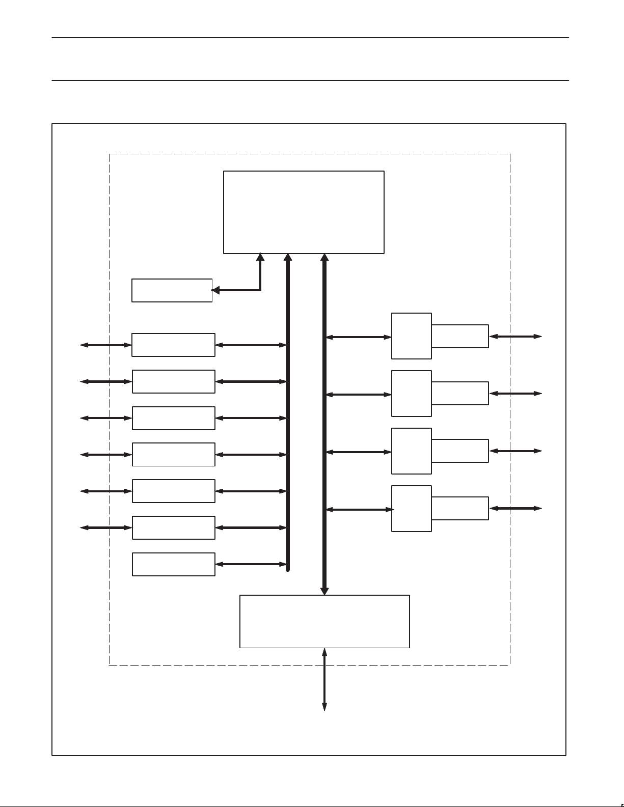
XA-H3 BLOCK DIAGRAM
XA-H3 CPU Core
256 Bytes Data
SRAM
Port 0
Port 1
Port 2
Port 3
Timer 0
Timer 1
Watchdog
Timer
Data
SFR Bus
MMR Bus
DMA R0
DMA T0
DMA R1
DMA T1
DMA R2
DMA T2
DMA R3
DMA T3
UART 0
UART 1
UART 2
UART 3
1999 Sep 24
Memory Bus Controller
6 Chip Selects
Dynamic Bus Sizing
Dynamic Bus Timing
External
System Bus
SU01247
5

Philips Semiconductors Preliminary specification
XA-H3CMOS 16-bit highly integrated microcontroller
XA-H3 MEMORY MAPS
FFFFFFh
6 MB *
Common Code
and Data Space
000000h
Unified Memory
(von Neuman architecture)
*In either memory architecture, the XA-H3 can support a maximum of
6 MB because each of six Chip Selects is capable of 1 MB each. In
Unified architecture, Code and Data can share the same physical
Memory Chip and address space.
Code Space + Data Space = 6 MB Maximum Total with 1 MB per Chip Select. Each CS
(and thus, 1 MB space) can support either Code or Data in Harvard architecture.
FFFFFFh
FFFFFFh
Dedicated
Code Space
Dedicated
Data Space
1999 Sep 24
000000h
Harvard Architecture
000000h
SU01248
6

Philips Semiconductors Preliminary specification
XA-H3CMOS 16-bit highly integrated microcontroller
PIN DESCRIPTIONS
Mnemonic
V
SS
V
DD
ResetIn 55 I
WAIT/
Size16
XTALIn 60 I
XTALOut 61 I Crystal 2: Output from the oscillator amplifier.
CS0 49 O
CS1 48 O Chip Select 1*: Chip Selects 1 through 5 come out of reset disabled. They function as normal chip
CS2 47 O Chip Select 2 *: Active low Chip Selects CS1 through CS5 come out of reset disabled. They can
CS3 46 O Chip Select 3 *: See Chip Select 2 for description.
See Pins 56, 57 for 2 additional Chip Selects
WE 50 O Write Enable: Goes active low during all bus write cycles only.
OE 51 O Output Enable: Goes active low during all bus read cycles only.
BLE 54 O Byte Low Enable: Goes active low during all bus cycles that access data bus lines D7 – D0, read
BHE 53 O Byte High Enable: Goes active low during all bus cycles that access data bus lines D15 – D8,
ClkOut 45 O Clock Output: This pin outputs a buffered version of the internal CPU clock. The clock output may
A19 – A0 24 – 21,
D15 – D0 42 – 30,
P0.0 90 I/O P0.0_BRG0*: Port 0 Bit 0, or UART0 BRG output, or UART0 TxClk output 1
P0.1 91 I/O P0.1_RTS0: Port 0 Bit 1 , or UART0 RTS (Request T o Send) output. 1
P0.2 92 I/O P0.2_CTS0: Port 0 Bit 2, or UART0 CTS (Clear T o Send) input. 1
P0.3 93 I/O P0.3_CD0: Port 0 Bit 3, or UART0 Carrier Detect input. 1
P0.4 94 I/O P0.4_TRClk0: Port 0 Bit 4, or UART0 TR clock input. 1, 2
P0.5 95 I/O P0.5_RTClk0 : Port 0 Bit 5, or UART0 RT clock input. 1, 2
P0.6 99 I/O P0.6: Port 0 Bit 6 1
P0.7 100 I/O P0.7: Port 0 Bit 7 1
TxD0 96 O TxD0: Transmit data for UART0.
Lqfp
Pin No.
1, 19, 28,
44, 59,
76, 88
2, 20, 29,
43, 62,
77, 89
52 I
18 – 3
27 – 25
Type Name and Function
Ground: 0 V reference.
I
Power Supply: This is the power supply voltage for normal, idle, and power down operation.
I
Reset: A low on this pin resets the microcontroller, causing I/O ports and peripherals to take on
their default states, and the processor to begin execution at the address contained in the reset
vector.
Wait/Size16: During Reset, this input determines bus size for boot device (“1” = 16-bit boot device;
“0” = 8-bit.) During normal operation this is the Wait input (“1” = Wait; “0” = Proceed.)
Crystal 1: Input to the inverting amplifier used in the oscillator circuit and input to the internal clock
generator circuits.
Chip Select 0: This output provides the active low chip select to the boot device (usually ROM or
Flash.) From reset, it is enabled and mapped to an address range based at 000000h. It can be
remapped by software to a higher base in the address map (see the “Memory Interface” chapter in
XA-H3 User Manual
the
selects on the H3. CS1 can be “swapped” with CS0 (see the SWAP operation in the “Memory
Controller” chapter of the
after the swap, but is capable of being based anywhere in the 16 MB address space.
be programmed to function as normal chip selects. CS2 through CS5 are not used with the
“SWAP” operation (only /CS0 and CS1 can be swapped; see “Memory Controller” chapter in the
XA-H3 User Manual
or write.
read or write. Never goes active on an 8-bit bus; always goes active on Reads or Fetches on a
16-bit bus, even if the processor does not need these bits. In other words, all Reads (byte or word)
on a 16-bit bus, assert BHE
be used in conjunction with the external bus to synchronize WAIT state generators, etc. The clock
output may be disabled by software. WARNING: The capacitive loading on this output must not
exceed 40 pf.
O Address[19:0]: These address lines output A19 – A0 during all external bus cycles.
I/O Data[15:0]: Bi-directional data bus, D15 – D0; for those bus cycles that are programmed to occur
on an “8-bit bus”, D15 – D8 are unused.
.)
XA-H3 User Manual
.) They are mappable to any region of the 16 MB address space.
.
.) CS1 is usually mapped to be based at 000000h
See
Note
1999 Sep 24
7

Philips Semiconductors Preliminary specification
XA-H3CMOS 16-bit highly integrated microcontroller
Mnemonic
RxD0 97 I RxD0: Receive data for UART0
GPOut 98 O GPOut – General Purpose Output Bar: Similar to GPIO, but Push/Pull and inverted output only.
P1.0 68 I/O P1.0_RxD2: Port 1 Bit 0, or UART2 RxD input
P1.1 69 I/O P1.1_TxD2: Port 1 Bit 1, or UART2 TxD output
P1.2 70 I/O P1.2_RTClk2 : Port 1 Bit 2, or UART2 RT Clock input 2
P1.3 71 I/O P1.3_TRClk2: Port 1 Bit 3, or UART2 TR Clock input 2
P1.4 72 I/O P1.4_CD2: Port 1 Bit 4, or UART2 Carrier Detect input
P1.5 73 I/O P1.5_CTS2: Port 1 Bit 5, or UART2 Clear T o Send input
P1.6 74 I/O P1.6_RTS2: Port 1 Bit 6, or UART2 Request T o Send output
P1.7 75 I/O P1.7_BRG2: Port 1 Bit 7, or BRG output, or TxClk output (see UART clk diagrams in the
P2.0 80 I/O P2.0_RxD3: Port 2 Bit 0, or UART3 Rx Data input
P2.1 81 I/O P2.1_TxD3: Port 2 Bit 1, or UART3 Tx Data output
P2.2 82 I/O P2.2_RTClk3 : Port 2 Bit 2, or UART3 RT Clock input 2
P2.3 83 I/O P2.3_ComClk_TRClk3: Port 2 Bit 3, or UART3 TR Clock input 2
P2.4 84 I/O P2.4_CD3: Port 2 Bit 4, or UART3 Carrier Detect input
P2.5 85 I/O P2.5_CTS3: Port 2 Bit 5, or UART3 Clear T o Send input
P2.6 86 I/O P2.6_RTS3: Port 2 Bit 6, or UART3 Request T o Send output
P2.7 87 I/O P2.7_BRG3: Port 2 Bit 7, or BRG output, or TxClk output (see UART clock diagrams in the
P3.0 56 I/O P3.0_CS4_RTClk1: Port 3 Bit 0, or CS4 output, or UART1 RT Clock input
P3.1 57 I/O
P3.2 58 I/O
P3.3 63 I/O P3.3_Timer1_BRG1: Port 3 Bit 3, or Timer1 input or output, or UART1 BRG output.
P3.4 64 I/O P3.4_CTS1: Port 3 Bit 4, or UART1 Clear T o Send input
P3.5 65 I/O P3.5_RxD1: Port 3 Bit 5, or UART1 Receive Data input
P3.6 66 I/O P3.6_TxD1: Port 3 Bit 6, or UART1 Transmit Data output
P3.7 67 I/O P3.7_Int1 _TRClk1: Port 3 Bit 7, or External Interrupt 1 input, or UART1 TR Clock input 2
CD1_Int2 78 I/O CD1_Int2: UART1 Carrier Detect, or External Interrupt 2
Int0 79 I/O External Interrupt 0
Lqfp
Pin No.
Name and FunctionType
WARNING: This output is inverted. The polarity of the pin is the opposite of the bit that drives it
(GPOut[7])
XA-H3
User Manual
.)
XA-H3
User Manual
Active low chip selects CS1 through CS5 come out of reset disabled. CS2 through CS5 are not
used with the “SWAP” operation (see “Memory Controller” chapter in the
They are mappable to any region of the 16 MB address space.
P3.1_CS5_RTS1: Port 3 Bit 1, or CS5 output, or UART1 Request To Send output
Active low chip selects CS1 through CS5 come out of reset disabled. CS2 through CS5 are not
used with the “SWAP” operation (see “Memory Controller” chapter in the
They are mappable to any region of the 16 MB address space.
P3.2_Timer0_ResetOut: Port 3 Bit 2, or Timer0 input or output, or ResetOut output.
ResetOut: If the ResetOut function is selected, this pin outputs a low whenever the XA-H3
processor is reset by an internal source (Watchdog Reset or the RESET instruction.)
WARNING: Unlike the other 31 GPIO pins, during power up reset, this pin can output a strongly
driven low pulse. The duration of this low pulse ranges from 0 ns to 258 system clocks, starting at
the time that VCC is valid. The state of the ResetIn
ResetIn
When used as GPIO, this pin can also be driven low by software without resetting the XA-H3.
.)
is not passed to ResetOut.
XA-H3 User Manual
XA-H3 User Manual
pin does not affect this pulse; in other words
.)
.)
See
Note
2
NOTES:
1. See
XA-H3 User Guide,
2. RTClk input is usually used for Rx Clock if an external clock is needed, but can be used for either Rx or Tx or both. TRClk is usually used for
Tx Clock, but can be used for Rx or Tx or both.
1999 Sep 24
“Pins Chapter,” for how to program selection of pin functions.
8

Philips Semiconductors Preliminary specification
writing BTRL
40h in that order. Follow these two writes with five NOPS. This is
XA-H3CMOS 16-bit highly integrated microcontroller
CONTROL REGISTER OVERVIEW
There are two types of control registers in the XA-H3, these are SFRs
(Special Function Registers), and MMRs (Memory Mapped Registers.)
The SFR registers, with the exception of MRBL, MRBH, MICFG, BCR,
BRTH, BRTL, and RSTSRC are the standard XA core registers. See
WARNINGs about BCR, BRTH, and BRTL in Table 2.
SFRs are accessed by “direct addressing” only (see
Manual
for direct addressing.) The MMRs are specific to the XA-H3
IC25 XA User
Table 2. Special Function Registers (SFR)
Name Description
BCR Bus Configuration Reg
RESERVED – see
Warning
BTRH Bus Timing Reg High 469h
BTRL Bus Timing Reg Low 468h
SFR
Address
46Ah WARNING – Never write to the BCR register in the XA-H3 – it is initialized to 07h,
MSB LSB
the only legal value. This is not the same as for some other XA derivatives.
WARNING – Immediately after reset, always write BTRH = 51h, followed by
=
not the same as for some other XA derivatives.
on-chip peripherals, and can be accessed by any addressing mode
that can be used for off-chip data accesses. The MMRs are
implemented in a relocatable block. See the “Memory Controller”
chapter in the
MMRs by writing a new base address into the MRBL and MRBH
(MMR Base Low and High) registers.
Bit Functions and Addresses
XA-H3 User Manual
for details on how to relocate the
Reset
Value
07h
FFh
EFh
MRBL# MMR Base Address Low 496h MA15 MA14 MA13 MA12 – – – MRBE x0h
MRBH# MMR Base Address High 497h MA23 MA22 MA21 MA20 MA19 MA18 MA17 MA16 xx
MICFG# ClkOut Tri-St Enable
1 = Enabled
CS Code Segment 443h 00h
DS Data Segment 441h 00h
ES Extra Segment 442h 00h
IEH* Interrupt Enable High 427h
IEL* Interrupt Enable Low 426h EA EDMAH EDMAL EX2 ET1 EX1 ET0 EX0 00h
IPA0 Interrupt Priority A0 4A0h – PT0 – PX0 00h
IPA1 Interrupt Priority A1 4A1h – PT1 – PX1 00h
IPA2 Interrupt Priority A2 4A2h – PDMAL – PX2 00h
IPA3 Interrupt Priority A3 4A3h Reserved – PDMAH 00h
IPA4 Interrupt Priority A4 4A4h – PSC23 – PSC01 00h
IPA5 Interrupt Priority A5 4A5h – – – PAutoB 00h
IPA6 Interrupt Priority A6 4A6h – PHSWR1 – PHSWR0 00h
IPA7 Interrupt Priority A7 4A7h – PHSWR3 – PHSWR2 00h
499h – – – – – – – CLKOE 01h
33F 33E 33D 33C 33B 33A 339 338
EHSWR3 EHSWR2 EHSWR1 EHSWR0 – EAuto ESC23 ESC01
337 336 335 334 333 332 331 330
00h
387 386 385 384 383 382 381 380
P0* Port 0 430h FFh
38F 38E 38D 38C 38B 38A 389 388
P1* Port 1 431h FFh
397 396 395 394 393 392 391 390
P2* Port 2 432h FFh
39F 39E 39D 39C 39B 39A 399 398
P3* Port 3 433h FFh
1999 Sep 24
9
Philips Semiconductors Preliminary specification
XA-H3CMOS 16-bit highly integrated microcontroller
Name
P0CFGA Port 0 Configuration A 470h 5
P1CFGA Port 1 Configuration A 471h 5
P2CFGA Port 2 Configuration A 472h 5
P3CFGA Port 3 Configuration A 473h 5
P0CFGB Port 0 Configuration B 4F0h 5
P1CFGB Port 1 Configuration B 4F1h 5
P2CFGB Port 2 Configuration B 4F2h 5
P3CFGB Port 3 Configuration B 4F3h 5
PCON* Power Control Reg 404h – – – – – – PD IDL 00h
PSWH* Program Status Word High 401h SM TM RS1 RS0 IM3 IM2 IM1 IM0 2
PSWL* Program Status Word Low 400h C AC – – – V N Z 2
PSW51* 80C51 Compatible PSW 402h C AC F0 RS1 RS0 V F1 P 3
Description
SFR
Address
MSB LSB
227 226 225 224 223 222 221 220
20F 20E 20D 20C 20B 20A 209 208
207 206 205 204 203 202 201 200
217 216 215 214 213 212 211 210
Bit Functions and Addresses
Reset
Value
RSTSRC Reset Source Reg 463h ROEN – – – – R_WD R_CMD R_EXT 7
RTH0 Timer 0 Reload High 455h 00h
RTH1 Timer 1 Reload High 457h 00h
RTL0 Timer 0 Reload Low 454h 00h
RTL1 Timer 1 Reload Low 456h 00h
SCR System Configuration Reg 440h – – – – PT1 PT0 CM PZ 00h
21F 21E 21D 21C 21B 21A 219 218
SSEL* Segment Selection Reg 403h ESWEN R6SEG R5SEG R4SEG R3SEG R2SEG R1SEG R0SEG 00h
SWE Software Interrupt Enable 47Ah – SWE7 SWE6 SWE5 SWE4 SWE3 SWE2 SWE1 00h
357 356 355 354 353 352 351 350
SWR* 42Ah – SWR7 SWR6 SWR5 SWR4 SWR3 SWR2 SWR1 00h
287 286 285 284 283 282 281 280
TCON* Timer 0/1 Control 410h TF1 TR1 TF0 TR0 IE1 IT1 IE0 IT0 00h
TH0 Timer 0 High 451h 00h
TH1 Timer 1 High 453h 00h
TL0 Timer 0 Low 450h 00h
TL1 Timer 1 Low 452h 00h
TMOD Timer 0/1 Mode 45Ch GATE C/T M1 M0 GATE C/T M1 M0 00h
1999 Sep 24
10

Philips Semiconductors Preliminary specification
XA-H3CMOS 16-bit highly integrated microcontroller
Name
TSTAT* Timer 0/1 Extended Status 411h – – – – – T1OE – T0OE 00h
WDCON* Watchdog Control 41Fh PRE2 PRE1 PRE0 – – WDRUN WDTOF – 6
WDL W atchdog Timer Reload 45Fh 00h
WFEED1 Watchdog Feed 1 45Dh x
WFEED2 Watchdog Feed 2 45Eh x
NOTES:
* SFRs marked with an asterisk (*) are bit addressable.
# SFRs marked with a pound sign (#) are additional SFR registers specific to the XA-H3 and XA-H4.
1. The XA-H3 implements an 8-bit SFR bus, as stated in Chapter 8 of the
8-bit operations. Attempts to write 16 bits to an SFR will actually write only the lower 8 bits. 16-bit SFR reads will return undefined data in the
upper byte.
2. SFR is loaded from the reset vector.
3. F1, F0, and P reset to “0”. All other bits are loaded from the reset vector.
4. Unimplemented bits in SFRs are “X” (unknown) at all times. “1”s should not be written to these bits since they may be used for other
purposes in future XA derivatives. The reset value shown for these bits is “0”.
5. Port configurations default to quasi-bidirectional when the XA begins execution after reset. Thus all PnCFGA registers will contain FFh and
PnCFGB register will contain 00h. See warning in
up. Basically, during this period, this pin may output a strongly-driven low pulse. If the pulse does occur, it will terminate in a transition to high
at a time no later than the 259th system clock after valid V
6. The WDCON reset value is E6 for a Watchdog reset; E4 for all other reset causes.
7. The RSTSRC register reflects the cause of the last XA reset. One bit will be set to “1”, the others will be “0”. RSTSRC[7] enables the ResetOut
function; “1” = Enabled, “0” = Disabled. See
8. The XA guards writes to certain bits (typically interrupt flags) that may be written by a peripheral function. This prevents loss of an interrupt or
other status if a bit was written directly by a peripheral action between the read and write of an instruction that performs a read-modify-write
operation. XA-H3 SFR bits that are guarded in this manner are: TF1, TF0, IE1, and IE0 (in TCON), and WDTOF (in WDCON).
Description
SFR
Address
XA-H3 User Manual
XA-H3 User Manual
MSB LSB
28F 28E 28D 28C 28B 28A 289 288
2FF 2FE 2FD 2FC 2FB 2FA 2F9 2F8
power up.
CC
for details; RSTSRC[7] differs in function from most other XA derivatives.
Bit Functions and Addresses
IC25 Data Handbook XA User Guide
about P3.2_Timer0_ResetOut pin during first 258 clocks after power
. All SFR accesses must be
Reset
Value
1999 Sep 24
11
 Loading...