

Philips VR340/55, VR740/55, VR340/75, VR740/75 Service Manual
Video Cassette Recorder
VR340/55
VR340/75
Service
VR740/55
VR740/75
Service
Service
/
STOP/EJECT
FWD.PLAYREW.RECORD
STANDBY/ON
CHANNEL
STANDBY/ON
STOP/EJECT
/
VR340/55/75 VR740/55/75
FWD.PLAYREW.RECORD
CHANNEL
Service Manual
Contents
Chapter
Specifications
Sec. 1:
Adjustment Procedure
Schematic Diagrams and CBA's
Exploded Views
Mechanical and Electrical Parts Lists
Sec. 2:
Standard Maintenance
Mechanism Alignment Procedures
Disassembly / Assembly of Mechanism
Deck Exploded Views
Survey of types:
VR340, VR740: Video Cassette Recorder
Survey of versions:
/55/75 PAL
Safety regulations require that the set be restored to its original
condition and that parts which are identical with those specified
be used.
Published by BK 2003 Video Service Department Printed in Japan c Copyright reserved Subject to modification GB 3103 785 22210

MAIN SECTION
VIDEO CASSETTE RECORDER
Sec. 1: Main Section
I Specifications
I Adjustment Procedures
I Schematic Diagrams and CBA’s
I Exploded Views
I Mechanical and Electrical Parts List
TABLE OF CONTENTS
SPECIFICATIONS. . . . . . . . . . . . . . . . . . . . . . . . . . . . . . . . . . . . . . . . . . . . . . . . . . . . . . . . . . . . . . . . . . . . . . . 1-1-1
IMPORTANT SAFETY PRECAUTIONS . . . . . . . . . . . . . . . . . . . . . . . . . . . . . . . . . . . . . . . . . . . . . . . . . . . . . . 1-2-1
STANDARD NOTES FOR SERVICING. . . . . . . . . . . . . . . . . . . . . . . . . . . . . . . . . . . . . . . . . . . . . . . . . . . . . . .1-3-1
FUNCTION INDICATOR SYMBOLS . . . . . . . . . . . . . . . . . . . . . . . . . . . . . . . . . . . . . . . . . . . . . . . . . . . . . . . . . 1-4-1
PREPARATION FOR SERVICING . . . . . . . . . . . . . . . . . . . . . . . . . . . . . . . . . . . . . . . . . . . . . . . . . . . . . . . . . .1-5-1
OPERATING CONTROLS AND FUNCTIONS. . . . . . . . . . . . . . . . . . . . . . . . . . . . . . . . . . . . . . . . . . . . . . . . . . 1-6-1
SIGNAL NAME ABBREVIATIONS. . . . . . . . . . . . . . . . . . . . . . . . . . . . . . . . . . . . . . . . . . . . . . . . . . . . . . . . . . . 1-7-1
CABINET DISASSEMBLY INSTRUCTIONS . . . . . . . . . . . . . . . . . . . . . . . . . . . . . . . . . . . . . . . . . . . . . . . . . . .1-8-1
ELECTRICAL ADJUSTMENT INSTRUCTIONS . . . . . . . . . . . . . . . . . . . . . . . . . . . . . . . . . . . . . . . . . . . . . . . .1-9-1
Adjustment Points and Test Points . . . . . . . . . . . . . . . . . . . . . . . . . . . . . . . . . . . . . . . . . . . . . . . . . . . . . . . . 1-9-2
BLOCK DIAGRAMS. . . . . . . . . . . . . . . . . . . . . . . . . . . . . . . . . . . . . . . . . . . . . . . . . . . . . . . . . . . . . . . . . . . . . 1-10-1
SCHEMATIC DIAGRAMS / CBA’S AND TEST POINTS . . . . . . . . . . . . . . . . . . . . . . . . . . . . . . . . . . . . . . . . . 1-11-1
Main 1/5 Schematic Diagram Parts Location Guide. . . . . . . . . . . . . . . . . . . . . . . . . . . . . . . . . . . . . . . . . . 1-11-2
Main 1/5 Schematic Diagram . . . . . . . . . . . . . . . . . . . . . . . . . . . . . . . . . . . . . . . . . . . . . . . . . . . . . . . . . . . 1-11-3
Main 2/5 & Sensor & SW1 & SW2 Schematic Diagram . . . . . . . . . . . . . . . . . . . . . . . . . . . . . . . . . . . . . . . 1-11-5
Main 2/5 Schematic Diagram Parts Location Guide. . . . . . . . . . . . . . . . . . . . . . . . . . . . . . . . . . . . . . . . . . 1-11-7
Main 3/5 Schematic Diagram Parts Location Guide . . . . . . . . . . . . . . . . . . . . . . . . . . . . . . . . . . . . . . . . . 1-11-8
Main 3/5 Schematic Diagram . . . . . . . . . . . . . . . . . . . . . . . . . . . . . . . . . . . . . . . . . . . . . . . . . . . . . . . . . . . 1-11-9
Main 4/5 Schematic Diagram . . . . . . . . . . . . . . . . . . . . . . . . . . . . . . . . . . . . . . . . . . . . . . . . . . . . . . . . . . 1-11-11
Main 4/5 Schematic Diagram Parts Location Guide. . . . . . . . . . . . . . . . . . . . . . . . . . . . . . . . . . . . . . . . . 1-11-13
Main 5/5 Schematic Diagram Parts Location Guide. . . . . . . . . . . . . . . . . . . . . . . . . . . . . . . . . . . . . . . . . 1-11-14
Main 5/5 Schematic Diagram (C,D) . . . . . . . . . . . . . . . . . . . . . . . . . . . . . . . . . . . . . . . . . . . . . . . . . . . . . 1-11-15
AFV Schematic Diagram (C,D). . . . . . . . . . . . . . . . . . . . . . . . . . . . . . . . . . . . . . . . . . . . . . . . . . . . . . . . . 1-11-17
Main CBA Top View . . . . . . . . . . . . . . . . . . . . . . . . . . . . . . . . . . . . . . . . . . . . . . . . . . . . . . . . . . . . . . . . . 1-11-19
Main CBA Bottom View. . . . . . . . . . . . . . . . . . . . . . . . . . . . . . . . . . . . . . . . . . . . . . . . . . . . . . . . . . . . . . . 1-11-21
Main CBA Parts Location Guide . . . . . . . . . . . . . . . . . . . . . . . . . . . . . . . . . . . . . . . . . . . . . . . . . . . . . . . 1-11-23
SW1 & SW2 & AFV CBA Top/Bottom View . . . . . . . . . . . . . . . . . . . . . . . . . . . . . . . . . . . . . . . . . . . . . . . 1-11-25
WAVEFORMS . . . . . . . . . . . . . . . . . . . . . . . . . . . . . . . . . . . . . . . . . . . . . . . . . . . . . . . . . . . . . . . . . . . . . . . . .1-12-1
WIRING DIAGRAM . . . . . . . . . . . . . . . . . . . . . . . . . . . . . . . . . . . . . . . . . . . . . . . . . . . . . . . . . . . . . . . . . . . . . 1-13-1
SYSTEM CONTROL TIMING CHARTS . . . . . . . . . . . . . . . . . . . . . . . . . . . . . . . . . . . . . . . . . . . . . . . . . . . . . 1-14-1
IC PIN FUNCTION DESCRIPTIONS. . . . . . . . . . . . . . . . . . . . . . . . . . . . . . . . . . . . . . . . . . . . . . . . . . . . . . . . 1-15-1
LEAD IDENTIFICATIONS . . . . . . . . . . . . . . . . . . . . . . . . . . . . . . . . . . . . . . . . . . . . . . . . . . . . . . . . . . . . . . . . 1-16-1
ELECTRICAL PARTS LIST . . . . . . . . . . . . . . . . . . . . . . . . . . . . . . . . . . . . . . . . . . . . . . . . . . . . . . . . . . . . . . . 1-17-1
EXPLODED VIEWS. . . . . . . . . . . . . . . . . . . . . . . . . . . . . . . . . . . . . . . . . . . . . . . . . . . . . . . . . . . . . . . . . . . . .1-18-1
SET MECHANICAL PARTS LIST . . . . . . . . . . . . . . . . . . . . . . . . . . . . . . . . . . . . . . . . . . . . . . . . . . . . . . . . . . 1-19-1
VR340CV
SPECIFICATIONS
Comparison Chart of Models and Marks
Model Mark
VR340/55 A
VR340/75 B
VR740/55 C
VR740/75 D
Description Unit Minimum Nominal Maximum Remark
1. Video
1-1. Video Output (PB) Vp-p 0.8 1.0 1.2 SP Mode
1-2. Video Output (R/P) Vp-p 0.8 1.0 1.2
1-3. Video S/N Y (R/P) dB 40 45
1-4. Video Color S/N AM (R/P) dB 37 41 SP Mode
1-5. Video Color S/N PM (R/P) dB 30 36 SP Mode
1-6. Resolution (PB) Line 230 245 SP Mode
2. Servo
2-1. Jitter Low µsec 0.07 0.12 SP Mode
2-2. Wow & Flutter % 0.3 0.5 SP Mode
3. Normal Audio
3-1. Output (PB) dBV -9 -6 -3 SP Mode
3-2. Output (R/P) dBV -9 -6 -1.5 SP Mode
3-3. S/N (R/P) dB 36 41 SP Mode
3-4. Distortion (R/P) % 1.0 4.0 SP Mode
3-5. Freq. resp (R/P) at 200Hz dB -7 -4 SP Mode
(-20dB ref. 1kHz) at 6kHz dB -10 -4 SP Mode
4. Tuner
4-1. Video output Vp-p 0.8 1.0 1.2 E-E Mode
4-2. Video S/N dB 39 42 E -E Mode
SP Mode,
W/O Burst
4-3. Audio output dB -10 -6 -2 E-E Mode
4-4. Audio S/N dB 40 46 E-E Mode
5. Hi-Fi Audio [ C, D ]
5-1. Output dBV -12 -8 -4 SP Mode
5-2. Dynamic Range dB 70 85 SP Mode
5-3. Freq. resp (6dB B.W) Hz 20 ~ 20K SP Mode
Note: Nominal specs represent the design specs. All units should be able to approximate these – some will exceed
and some may drop s lightly bel ow these spec s. Limit sp ecs rep resent the a bsolute wo rst con dition that still migh t
be considered acceptable; In no case should a unit fail to meet limit specs.
1-1-1 HE274SP

IMPORTANT SAFETY PRECAUTIONS
Product Safety Notice
Some electrical and mechanical parts have special
safety-related charac teristics which are often not evident from visual inspection, nor can the protection
they give necessarily be obtained by replacing them
with components rated for higher voltage, wattage,
etc. Parts that have spe cial safety characteristics are
identified by a ! on schematics and in parts lists. Use
of a substitute replacement that does not have the
same safety characteristics as the recommended
replacement part might create shock, fire, and/or other
hazards. The Pro duct’s Safety is und er review con tinuously and new instructions are issued whenever
appropriate. Prior to shipment from the factory, our
products are carefully inspected to confirm with the
recognized product s afety and electrical codes of the
countries in which they are to be sold. However, in
order to maintain such comp lianc e, it is equ ally impor tant to implement the following precautions when a set
is being serviced.
Precautions during Servicing
A. Parts identified by the ! symbol are critical for
safety. Replace only with part number specified.
B. In addition to safety, other parts and assemblies
are specified for conformance with regulations
applying to spur ious rad iation. T hese m ust also be
replaced only with specified re pla ce men ts.
Examples: RF converters, RF c ables, noise block-
ing capacitors, and noise blocking filters, etc.
C. Use specified internal wiring. Note especially:
1)Wires covered with PVC tubing
2)Double insulated wires
3)High voltage leads
D. Use specified insulating materials for hazardous
live parts. Note especially:
1)Insulation tape
2)PVC tubing
3)Spacers
4)Insulators for transistors
E. When replacing AC primary side components
(transformers, power cord, etc.), wrap ends of
wires securely about the terminals before solder-
ing.
F. Observe that the wir es do n ot co ntact h eat pr od uc -
ing parts (heatsinks, oxide metal fil m re sisto rs, fus -
ible resistors, etc.).
G. Check that replaced wires do not contact sharp
edges or pointed parts.
H. When a power cord h as been repl aced, ch eck that
5 - 6 kg of force in any direction will not loosen it.
I. Also check areas surrounding repaired locations.
J. Use care that foreign obj ects (screw s, solder drop-
lets, etc.) do not remain inside the set.
K. Crimp type wire connector
The power tr ansformer uses crimp type connectors
which connect the power cord and the primary side
of the transformer. When replacing the transformer,
follow these steps carefully and precisely to prevent shock hazards.
Replacement procedure
1)Remove the old connector by cutting the wires at a
point close to the connector.
Important: Do not re-use a connector. (Discard it.)
2)Strip about 15 mm of the insulation from the ends
of the wires. If the wires are stranded, twist the
strands to avoid frayed conductors.
3)Align the lengths of the wires to be connected.
Insert the wires fully into the connector.
4)Use a crimping tool to crimp the metal sleeve at its
center. Be sure to crimp fully to th e complete closure of the tool.
L. When connecting or disconnecting the internal con-
nectors, first, disco nnect the AC plug from th e AC
outlet.
1-2-1 HE274SFTY
Safety Check after Servicing
1
B
Z
2
Examine the area surrounding the repaired location for
damage or deterio ration. Observe that screws , parts,
and wires have been returned to their original positions. Afterwards, do the following tests and confirm
the specified values to verify compliance with safety
standards.
1. Clearance Distance
When replacing primary circuit components, confirm
specified cleara nce distanc e (d) and (d’) between sol dered terminals, and between terminals and surrounding metallic parts. (See Fig. 1)
T able 1 : Ratings for selected area
Clearance
AC Line Voltage
110 to 240 V (Auto)
[ VR340/55, VR740/55 ],
240 V [ VR340/75, VR740/75 ]
Note: This table is unofficial and for reference only.
Be sure to confirm the precise values.
Distance
(d) (d’)
≥ 3 mm(d)
≥ 6 mm(d’)
2. Leakage Current Test
Confirm the specified (or lower) leakage current
between B (earth ground, power cord plug prongs)
and externally exposed accessible parts (RF terminals, antenna terminals, video and audio input and
output terminals, microphone jacks, earphone jacks,
etc.) is lower than or equal to the specified value in the
table below.
Measuring Method (Power ON) :
Insert load Z between B (earth ground, power cord
plug prongs) and exposed accessible parts. Use an
AC voltmeter to measure acr oss the ter minals of l oad
Z. See Fig. 2 and the following table.
Chassis or Secondary Conductor
Primary Circuit Terminals
dd'
Fig.
Exposed Accessible Part
AC Voltmeter
(High Impedance)
One side of
Power Cord Plug Prongs
Fig.
T able 2: Leakage current ratings for selected areas
AC Line Voltage Load Z Leakage Current (i)
2kΩ RES.
110 to 240 V (Auto)
[ VR340/55, VR740/55 ],
240 V [ VR340/75, VR740/75 ]
Note: This table is unofficial and for reference only. Be sure to confirm the precise values.
Connected in
parallel
50kΩ RES.
Connected in
parallel
1-2-2 HE274SFTY
i≤0.7mA AC Peak
i≤2mA DC
i≤0.7mA AC Peak
i≤2mA DC
One side of power cord
plug prongs (B) to:
RF or
Antenna terminals
A/V Input, Output
STANDARD NOTES FOR SERVICING
O
P
P
Circuit Board Indications
a. The output pin of the 3 pin Regulator ICs is indi-
cated as shown.
Top View
Input
ut
b. For other ICs, pin 1 and every fifth pin are indicated
as shown.
In
in 1
c. The 1st pin of every male connector is indicated as
shown.
in 1
Bottom View
5
10
How to Remove / Install Flat Pac k-IC
1. Removal
With Hot-Air Flat Pack-IC Desoldering Machine:.
(1) Prepare the hot-air flat pack-IC desoldering
machine, then apply hot air to the Flat Pack-IC
(about 5 to 6 seconds). (Fig. S-1-1)
Fig. S-1-1
(2) Remove the flat pack-IC with tweezers while apply-
ing the hot air.
(3) Bottom of the fla t pack-IC is fixed with glue to the
CBA; when removing entire fl at pack-IC, fir st apply
soldering iron to center of the fla t pack-IC and hea t
up. Then remove (glue will be melted). (Fig. S-1-6)
(4) Release the fl at pack-IC from the CBA using twee-
zers. (Fig. S-1-6)
Instructions for Connectors
1. When you c onn ect o r di scon nec t the FF C (Fl exib le
Foil Connector) cable, be sure to first disconnect
the AC cord.
2. FFC (Flexible Foil Connector) cable should be
inserted parallel into the connector, not at an angle.
FFC Cable
Connector
CBA
* Be careful to avoid a short circuit.
Caution:
1. Do not supply hot air to the chip parts around the
flat pack-IC for over 6 seconds because damage
to the chip parts may occur. Put masking tape
around the flat pack-IC to protect other parts from
damage. (Fig. S-1-2)
2. The flat pack-I C on th e CB A i s a ffixed with g lue , so
be careful not to break or damage the foil of each
pin or the solder lands under the IC when removing
it.
Hot-air
Flat Pack-IC
Desoldering
CBA
Masking
Tape
Tweezers
Machine
Flat Pack-IC
Fig. S-1-2
1-3-1 NOTE_1
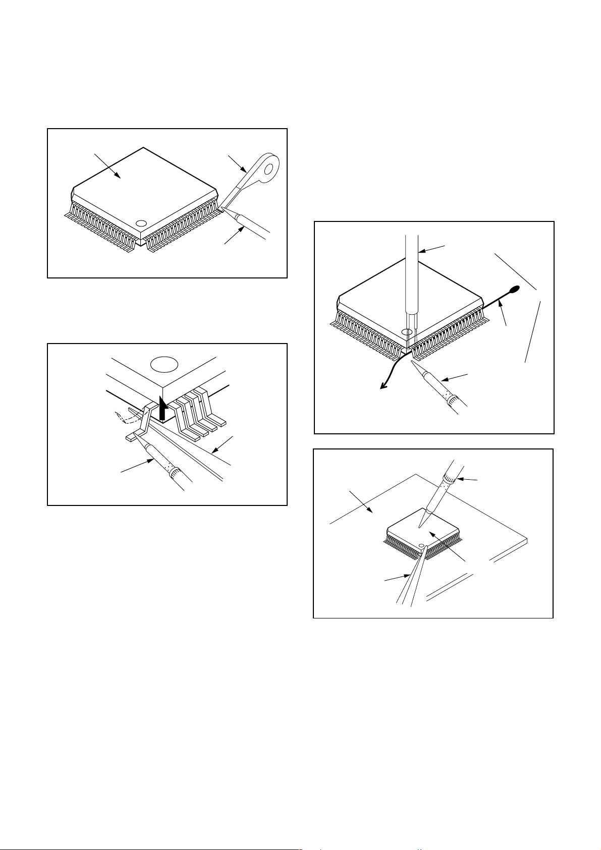
With Soldering Iron:
F
F
S
rp
or
n
(1)Using desoldering braid, remove the solder from all
pins of the flat pack-IC. Wh en you use solder flux
which is applied to all pins of the f lat pack-IC, you
can remove it easily. (Fig. S-1-3)
lat Pack-IC
Desoldering Braid
(4) Bottom of the fla t pack-IC is fixed with glue to the
CBA; when removing entire fl at pack-IC, fir st apply
soldering iron to center of the fla t pack-IC and hea t
up. Then remove (glue will be melted). (Fig. S-1-6)
(5) Release the fl at pack-IC from the CBA using twee-
zers. (Fig. S-1-6)
Note:
When using a sold ering iron, care must be taken
to ensure that the flat pack-IC is not being hel d by
glue. When the flat pack-IC is removed from the
CBA, handle it ge ntl y bec au se it may be damaged
if force is applied.
Soldering Iron
Hot Air Blower
Fig. S-1-3
(2) Lift each lead of the flat pack-IC upward one by
one, using a sharp pin or wire to which sold er will
not adhere (iron wir e). When heating the pins , us e
a fine tip soldering iron or a hot air desoldering
machine. (Fig. S-1-4)
Iron Wire
Soldering Iron
To Solid
Mounting Point
Fig. S-1-5
Sha
Pin
ine Tip
oldering Iron
Fig. S-1-4
CBA
Fine Tip
Soldering Iro
(3)Bottom of the flat pack-IC is fixed with glue to the
CBA; when removing enti re flat pack-IC, fi rst apply
soldering iron to c en ter o f th e f lat pack-I C an d h eat
up. Then remove (glue will be melted). (Fig. S-1-6)
(4)Release the flat pack-IC from the CBA us ing twee-
zers. (Fig. S-1-6)
Tweezers
Flat Pack-IC
With Iron Wire:
(1)Using desoldering braid, remove the solder from all
Fig. S-1-6
pins of the flat pack-IC. Wh en you use solder flux
which is applied to all pins of the f lat pack-IC, you
can remove it easily. (Fig. S-1-3)
(2) Affix the wire to a workbench or solid mounting
point, as shown in Fig. S-1-5.
(3) While heating the pins using a fine tip soldering
iron or hot air blower, pull up the wire as the solde r
melts so as to lift the IC leads from the CBA contact
pads as shown in Fig. S-1-5
1-3-2 NOTE_1
2. Installation
P
i
d
(1) Using desoldering braid, remove the solder from
the foil of each pin of the flat pack-IC on the CBA
so you can install a replac ement flat pack-IC more
easily.
(2)The “ I ” mark on the flat pack-IC indi cates pin 1.
(See Fig. S-1-7.) Be sure this mar k matches the 1
on the PCB when position ing for installation. Then
presolder the four corne rs of th e fla t pack-IC. (See
Fig. S-1-8.)
(3)Solder all pins of the flat pack-IC. Be sure that none
of the pins have solder bridges.
Example :
in 1 of the Flat Pack-IC
s indicated by a " " mark.
Fig. S-1-7
Instructions for Handling
Semi-conductors
Electrostatic breakdown of the semi-conductors may
occur due to a po tential difference ca used by electr ostatic charge during unpacking or repair work.
1. Ground for Human Body
Be sure to wear a gr oundin g band (1MΩ) that is properly grounded to re move any static electricity th at m ay
be charged on the body.
2. Ground for Workbench
Be sure to place a c onductive sheet or copper plate
with proper grounding (1MΩ) on the workbench or
other surface, where the semi-conductors are to be
placed. Because the static electricity charge on clo thing will not escape through the body grounding band ,
be careful to avoid contacting semi-conductors with
your clothing.
< Incorrect >
CBA
Presolder
Flat Pack-IC
Fig. S-1-8
CBA
< Correct >
Grounding Ban
1MΩ
CBA
1MΩ
Conductive Sheet or
Copper Plate
1-3-3 NOTE_1
FUNCTION INDICATOR SYMBOLS
Note:
The following symb ol s wil l appear on the indica tor panel to ind icate the current mode or o per at ion of the VCR.
On-screen modes will also be momentarily displayed on the tv screen when you press the operation buttons.
Display panel
PWR. REC
" H "= LED Light on, " L "= LED Light off
LED MODE INDICATOR ACTIVE
CASSETTE "IN"
CASSETTE "OUT"
CLOCK " 88:88 ON
POWER ON " PWR." ON
REC " REC " ON
REC PAUSE " REC " Blinks at 0.8Hz interval
T-REC,OTR
When reel and capstan mechanism is not
functioning correctly
When tape loading mechanism is not functioning correctly
When cassette loading mechanism is not
functioning correctly
When the drum is not working properly
P-ON Power safety detection
" "
" "
" "
" "
" 1 "
" "
" 2 "
" "
" 3 "
" "
" 4 "
" "
" 5 "
ON
OFF
ON
(T-REC OFF,T-REC incomplete
Blinks at 0.8Hz interval)
Blinks at 0.8Hz interval
Blinks at 0.8Hz interval
Blinks at 0.8Hz interval
Blinks at 0.8Hz interval
Blinks at 0.8Hz interval
S-INH condition All modes Blinks at 0.8Hz interval
1-4-1 HE274FIS
PREPARATION FOR SERVICING
How to Enter the Service Mode
About Optical Sensors
Caution:
An optical sensor system is used for the Tape Start
and End Sensors on this equipment. Carefully read
and follow the instructions below. Otherwise the unit
may operate erratically.
What to do for preparation
Insert a tape into the D eck Mechanis m Assembly and
press the PLAY button. The tape will be loaded into
the Deck Mechanism Ass embly. Make sure the power
is on, connect TP507 (SENSOR INHIBITION) to GND.
This will stop the functio n of Tape Start Sensor, Tape
End Sensor and Reel Sensors . (If these TPs are connected before plugging in the unit, the function of the
sensors will stay valid.) See Fig. 1.
Note: Because the Tape End Sensors are inactive, do
not run a tape all the way to the start or the end of the
tape to avoid tape damage.
Q504
Q505
TP507
S-INH
Fig. 1
1-5-1 HE274PFS
)
PWR. REC
10
11
14
12
13
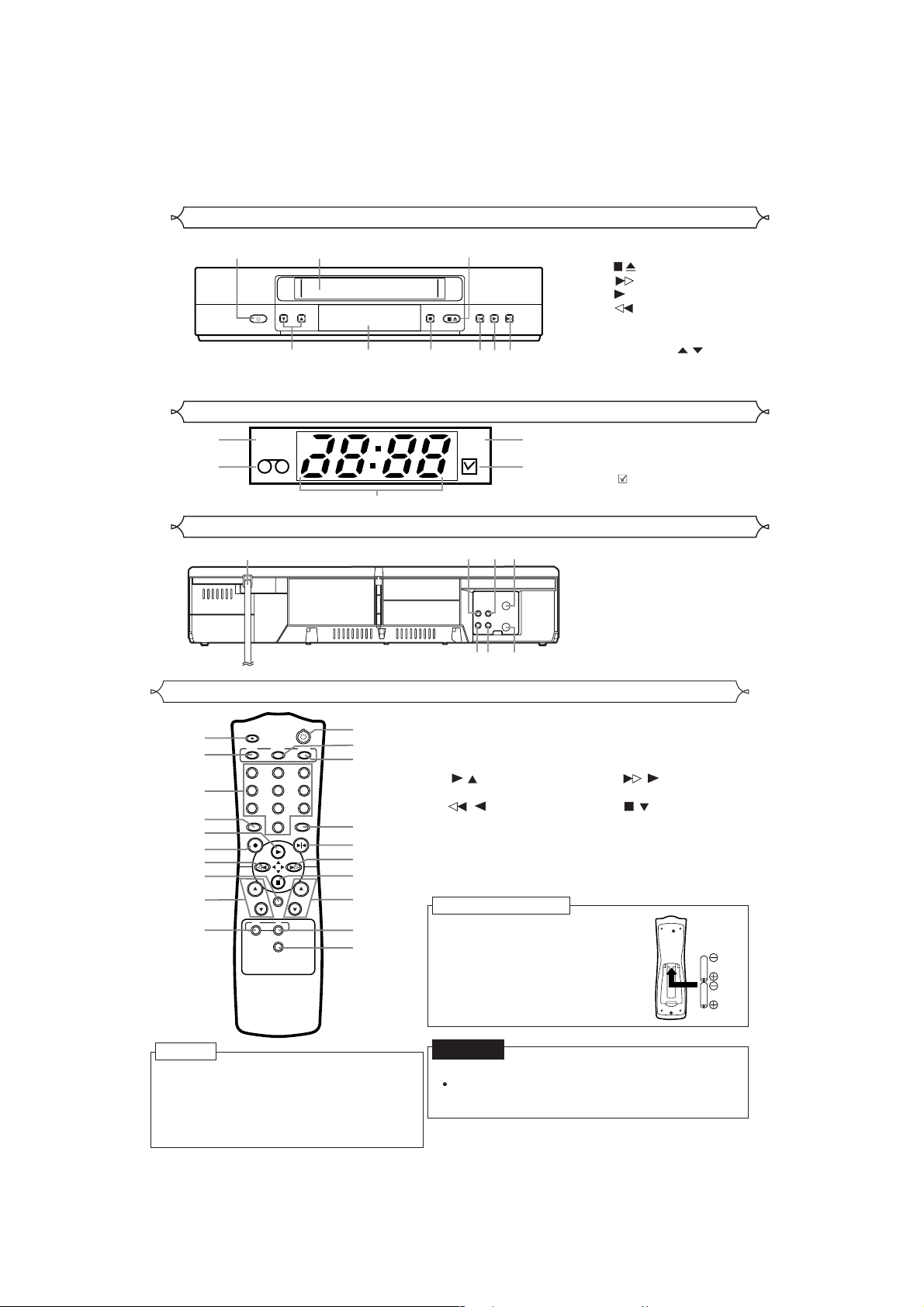
OPERATING CONTROLS AND FUNCTIONS
[ VR340/55 ]
Front Panel
1
STANDBY/ON
Indicator
Rear Panel
15
2
CHANNEL
STOP/EJECT
/
987 456
3
FWD.PLAYREW.RECORD
16 17 18
AUDIO
AERIAL
OUT IN
RF OUT
VIDEO
21 20 19
1. STANDBY/ON button
2. Cassette compartment
3.
[ / ] ( STOP/EJECT) button
4. [ ] (FWD)button
](PLAY) button
5. [
6. [ ](REW) button
7. RECORD button
8. Display window (See below
9. CHANNEL ( / ) buttons
10. PWR. (Power) indicator
11. TAPE IN indicator
12. REC indicator
13. (Timer) indicator
14. CLOCK indicator
15. AC power cord
16. AUDIO OUT jack
17. AUDIO IN jack
18. AERIAL terminal
19. RF OUT terminal
20. VIDEO IN jack
21. VIDEO OUT jack
Remote Control
EJECT
1
2
3
4
5
STANDBY/ON
MENU STATUS CLEAR
1 2 3
4 5 6
7 8
MEMORY ALT.CH
0
RECORD/OTR
9
STILL
6
7
8
9
10
NOTE
You can use this remote control to operate
some PHILIPS TVs. Press [VCR] before
pressing VCR feature buttons; press [TV] before
pressing TV feature buttons if you have a
PHILIPS TV .
CH. VOL.
MUTE
VCR TV
SPEED/SYSTEM
11
12
13
14
15
16
17
18
19
20
1. EJECT button
2. MENU button
3. NUMBER buttons
4. MEMORY button
5. [
( ) ](PLAY) button
6. RECORD/OTR button
7. [ (
) ](REW) button
8. MUTE button
9. CH(annel). buttons
10. VCR button
12. STATUS button
13. CLEAR button
14. ALT.CH.button
15. STILL button
16. [ (
) ](F .FWD)
button
17. [
( ) ](STOP) button
18. VOL(ume) buttons
19. TV button
SPEED/SYSTEM button
20.
11. STANDBY/ON button
To insert the batteries
Install two R6 batteries
matching the polarity
indicated inside the battery
compartment.
CAUTION
On Battery Replacement
Do not mix old and new batteries. (Also never mix
alkaline batteries with manganese batteries.)
1-6-1 HE274IB
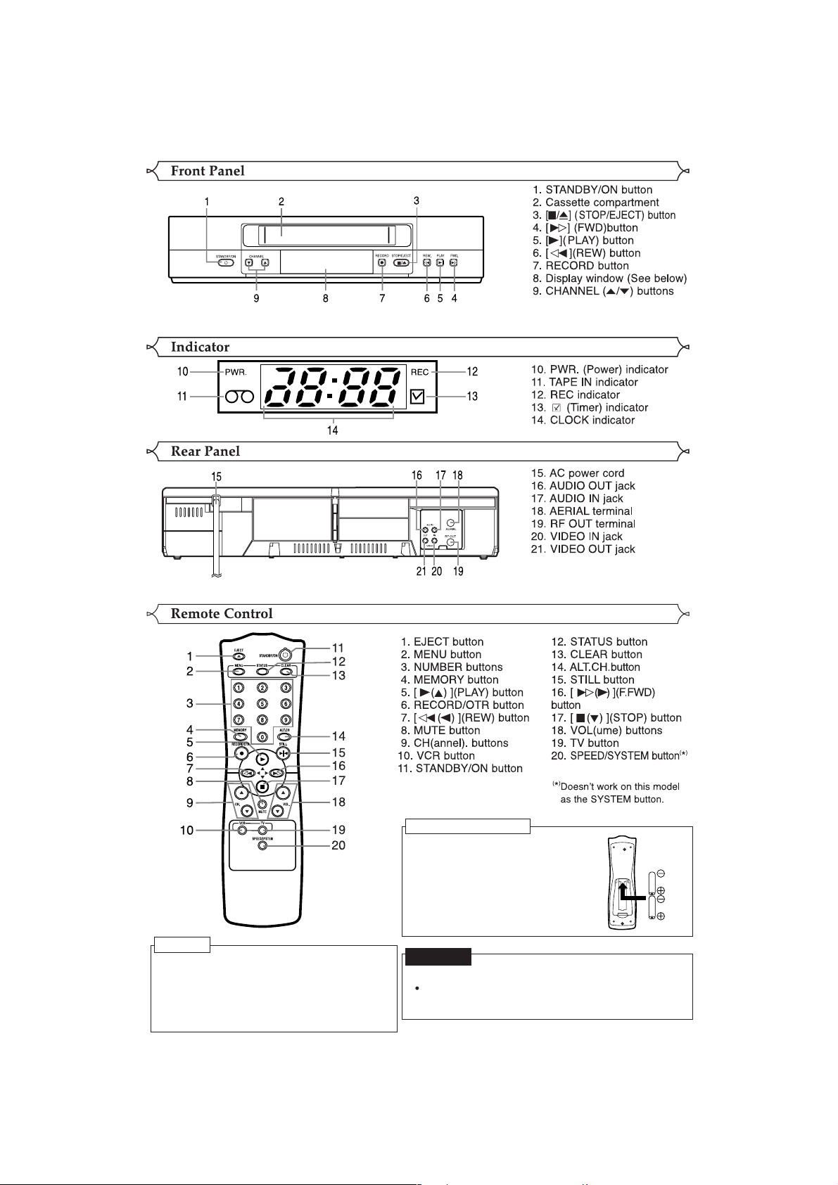
[ VR340/75 ]
NOTE
You can use this remote control to operate
some PHILIPS TVs. Press [VCR] before
pressing VCR feature buttons; press [TV] before
pressing TV feature buttons if you have a
PHILIPS TV .
To insert the batteries
Install two R6 batteries
matching the polarity
indicated inside the battery
compartment.
CAUTION
On Battery Replacement
Do not mix old and new batteries. (Also never mix
alkaline batteries with manganese batteries.)
1-6-2 HE274IB

)
PWR. REC
13
14
17
15
16
[ VR740/55 ]
Front Panel
1
STANDBY/ON
VIDEO
L-AUDIO-R
10
Indicator
Rear Panel
18
2
CHANNEL
987456
19 20 21
FWD.PLAYREW.RECORD
AUDIO
L
OUT
IN
AERIAL
R
VIDEO
RF OUT
OUT IN
22 23 24
STOP/EJECT
3
/
1. STANDBY/ON button
2. Cassette compartment
3.
[ / ] ( STOP/EJECT) button
4. [ ] (F.FWD)button
5. [
](PLAY) button
6. [ ](REW) button
7. RECORD button
8. Display window (See below
9. CHANNEL ( / ) buttons
10.A/V CONNECTORS
13. PWR. (Power) indicator
14. TAPE IN indicator
15. REC indicator
16. (Timer) indicator
17. CLOCK indicator
18. AC power cord
19. AUDIO OUT jacks
20. AUDIO IN jacks
21. AERIAL terminal
22. VIDEO OUT jack
23. VIDEO IN jack
24. RF OUT terminal
Remote Control
EJECT
1
2
3
4
5
STANDBY/ON
MENU STATUS CLEAR
1 2 3
4 5 6
7 8
MEMORY ALT.CH
0
RECORD/OTR
9
STILL
6
7
8
9
10
11
NOTE
You can use this remote control to operate
some PHILIPS TVs. Press [VCR] before
pressing VCR feature buttons; press [TV] before
pressing TV feature buttons if you have a
PHILIPS TV .
CH. VOL.
MUTE
VCR TV
SPEED/SYSTEM
TIME SEARCH
AUDIO SELECT
SLOW
12
13
14
15
16
17
18
19
20
21
22
23
To insert the batteries
Install two R6 batteries
matching the polarity
indicated inside the battery
compartment.
CAUTION
On Battery Replacement
Do not mix old and new batteries. (Also never mix
alkaline batteries with manganese batteries.)
1-6-3 HE274IB
[ VR740/75 ]
NOTE
You can use this remote control to operate
some PHILIPS TVs. Press [VCR] before
pressing VCR feature buttons; press [TV] before
pressing TV feature buttons if you have a
PHILIPS TV .
To insert the batteries
Install two R6 batteries
matching the polarity
indicated inside the battery
compartment.
CAUTION
On Battery Replacement
Do not mix old and new batteries. (Also never mix
alkaline batteries with manganese batteries.)
1-6-4 HE274IB
SIGNAL NAME ABBREVIATIONS
Signal Name Function
4.43MHz 4.43MHz Clock
A-COM Audio Head Common
A-IN Audio Signal Input
A-MODE Hi-Fi Tape Detection Signal
A-MUTE-H
A-OUT Audio Signal Output
A-PB/REC
AE-H Audio Erase Head
AFC
AL+12V
AL+5V
AMPC CTL AMP Connected Terminal
AMPVcc AMPVcc
AMPVREF
OUT
AMPVREF
AMPVss AMPVss
AVcc
C-CONT Capstan Motor Control Signal
C-F/R
C-FG
Audio Mute Control Signal
(Mute = “H”)
Normal Audio Play Back/Record
Signal
Automatic Frequency Control
Signal
Always +12V with AC Plug
Connected
Always +5V with AC Plug
Connected
V-Ref for CTL AMP
IN V-Ref for CTL AMP
A/D Converter Power Input/
Standard Voltage Input
Capstan Motor FWD/REV Control
Signal (FWD=”L”/REV=”H”)
Capstan Motor Rotation Detection
Pulse
Signal Name Function
D-PFG
Drum Motor Phase/Frequency
Generator
D-REC-H Delayed Record Signal
D-V- SYNC Dummy V-sync Output
DRV-CLK LED Clock Driver IC Control Clock
DRV-DATA LED Clock Driver IC Control Data
DRV-STB
LED Clock Driver IC Chip Select
Signal
END-S Tape End Position Detect Signal
FE-H GND Ground for Full Erase Head
FF/REW-L
FSC-IN
[4.43MHz ]
CTL Frequency Characteristics
Switching Signal (FF/REW=”L”)
4.43MHz Clock Input
H-A-COMP Head Amp Comparator Signal
H-A-SW Video Head Amp Switching Pulse
Hi-Fi-A Hi-Fi Audio Head
Hi-Fi-COM Hi-Fi Audio Head Common
HiFi-H-SW HiFi Audio Head Switching Pulse
HLF
2
C BUS- SCL I2C BUS Control Clock
I
2
I
C BUS- SDA I2C BUS Control Data
LPF Connected
Terminal (Slicer)
KEY-1 Key Scan Input Signal 1
KEY-2 Key Scan Input Signal 2
LD-SW
Deck Mode Position Detector
Signal
LM-FWD/REV Loading Motor Control Signal
C-ROTA
Color Phase Rotary Changeover
SIgnal
C-SYNC Composite Synchronized Pulse
CLKSEL Clock Select (GND)
SECAM or MESECAM Chroma
COLOR-IN
Video Input Signal at Super
Impose
CTL (+)
CTL (-)
Playback/Record Control Signal
(+)
Playback/Record Control Signal (-
)
CTLAMPout To Monitor for CTL AMP Output
D-CONT Drum Motor Control Signal
MOD-A Modulator Audio Output Signal
N-A-PB Normal Audio Playback
N-A-REC Normal Audio Recording
IN Clock Input for letter size
OSC
OUT Clock Output for letter size
OSC
OSD-V-IN OSD Video Signal Input
OSD-V-OUT OSD Video Signal Output
OSDVcc OSDVcc
OSDVss OSDVss
P-DOWN-L
Power Voltage Down Detector
Signal
1-7-1 HE274SNA

Signal Name Function
P-OFF-H Power Off at High
P-ON+5V +5V at Power-On Signal
P-ON-L Power On Signal at Low
P80/C P80/C Terminal
PG-DELAY
POW-SAF
REC-SAF-SW
REMOCON-IN Remote Control Sensor
RESET System Reset Signal (Reset=”L”)
RESET +5V +5V at System Reset Signal
RF-SW Video Head Switching Pulse
SIF Intermediate Frequency
ST-S
T-REEL Take Up Reel Rotation Signal
TIMER+5V +5V at Timer
TU-AUDIO Tuner Audio Input Signal
TU-VIDEO Tuner Video Input Signal
TUN-SW1
Video Head Switching Pulse
Signal Adjusted Voltage
P-ON Power Detection Input
Signal
Recording Safety SW Detect (With
Record tab="L"/With out Record
tab="H")
Tape Start Position Detector
Signal
Tuner System Control Signal
Output
TUN-SW2
V-ENV
V-IN Video Signal Input
V-OUT Video Signal Output
Vcc Vcc
VIDEO Video Signal
Vss Vss(GND)
X-IN Main Clock Input
X-OUT Main Clock Input
XC-IN Sub Clock
XC-OUT Sub Clock
Tuner System Control Signal
Output
Video Envelope Comparator
Signal
1-7-2 HE274SNA
CABINET DISASSEMBLY INSTRUCTIONS
Comparison Chart of Models and Marks
Model Mark
VR340/55 A
VR340/75 B
VR740/55 C
VR740/75 D
1. Disassembly Flowchart
This flowchart indicates the disassem bly steps to gain
access to item(s) to be serviced. When reassembling,
follow the steps in reverse order. Bend, route, and
dress the cables as they were originally.
[1] Top Case
[2] Front Assembly
[3] VCR Chassis Unit
[4] Deck Assembly
[5] Main CBA
(1): Identification (location) No. of parts in the figures
(2):Name of the part
(3):Figure Number for reference
(4): Identification of parts to be removed, unhooked,
unlocked, released, unplugged, unclamped, or
desoldered.
P=Spring, L=Locking Tab, S=Screw,
CN=Connector
*=Unhook, Unlock, Release, Unplug, or Desolder
e.g. 2(S-2) = two Screws (S-2),
2(L-2) = two Locking Tabs (L-2)
(5):Refer to “Reference Notes.”
Reference Notes
CAUTION: Locking Tabs (L-1) and (L-2) are fragile.
Be careful not to break them.
1. Remove five Screws (S-2), two Screws (S-3) and
Screw (S-4). Then, slowly lift the VCR Chassis Unit
(Deck Assembly, Jack CBA and Main CBA) up.
2. When reassembling, solder wire jumpers as shown
in Fig. 5.
3. Before installing the Deck Assembly, be sure to
place the pin of LD-SW on Main CBA as sho wn in
Fig. 6. Then, install the Deck Assembly while aligning the hole of Cam Gear with the pin of LD-SW,
the shaft of Cam Gear with the hole of LD-SW as
shown in Fig. 6.
2. Disassembly Method
REMOVAL
ID/
LOC.
No.
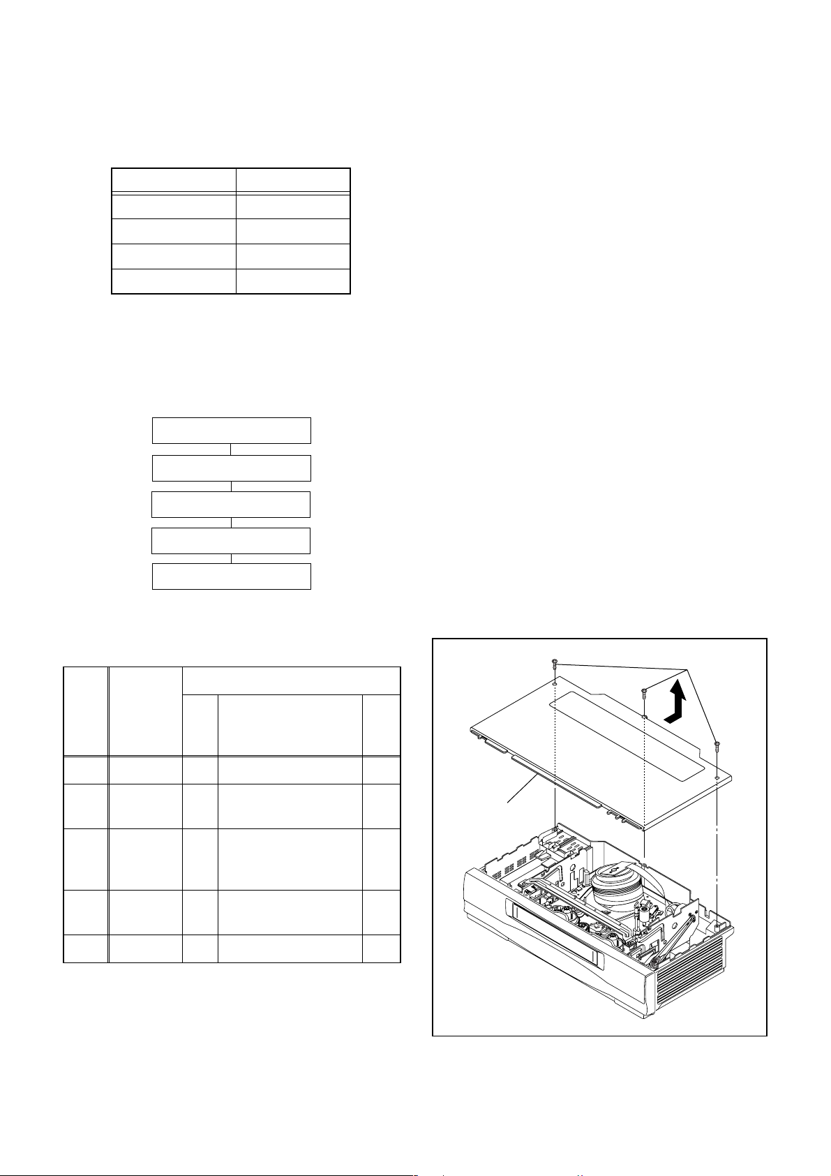
[1] Top Case 1 3(S-1) -
[2]
[3]
[4]
[5] Main CBA 4,5 ---------- -
↓
(1)
PART
Front
Assembly
VCR
Chassis
Unit
Deck
Assembly
↓
(2)
REMOVE/*UNHOOK/
Fig.
UNLOCK/RELEASE/
No.
UNPLUG/DESOLDER
2 *3(L-1),*4(L-2) -
5(S-2) ,
3
2(S-3)---[Mark: C, D]
3(S-4), 2(W-1),
4,5
Desolder
↓
(3)
↓
(4)
(S-1)
Note
[1] T op Case
1
2,3
↓
(5)
Fig. 1
1-8-1 HE274DC
(L-2)
(L-2)
FE Head
Cylinder
Assembly
[2] Front
Assembly
[3]VCR
Chassis Unit
(S-3)
(L-1)
(S-2)
(S-2)
Fig. 2
[4] Deck
Assembly
[5] Main CBA
From
Capstan
Motor
Assembly
(W-1)
(S-4)
From
ACE Head
Assembly
(S-4)
From
Cylinder
Assembly
ACE Head
Assembly
(W-1)
(S-4)
From
FE Head
[ C,D ]
(S-3)
[ C,D ]
Fig. 3
Printing
side
Desolder
Lead connections of Deck Assembly and Main CBA
Lead with
blue stripe
Desolder
BOTT OM VIEW
Lead with
blue stripe
Fig. 4
1-8-2 HE274DC
Pin
[5] Main CBA
[4] Deck Assembly
SW507
LD-SW
Cam Gear
LD-SW
Shaft
Hole
Hole
Pin
[5] Main CBA
Fig. 5
1-8-3 HE274DC
ELECTRICAL ADJUSTMENT INSTRUCTIONS
e
2
)
C
C
c
General Note: "CBA" is an abbreviation for
"Circuit Board Assembly."
NOTE:
1.Electrical adjus tments are required after replacing
circuit components a nd certain mechanical parts.
It is important to do these a djustments only after
all repairs and replacements have been completed. Also, do not attempt these adjustments
unless the proper equipment is available.
2.To perform these alignment / confirmation procedures, make sure that the tracki ng co ntrol is set in
the center position: P ress eith er "L5??" or "K" button
on the remote control unit first, then the "PLAY"
button (Front Panel only).
Test Equipment Required
1.Oscilloscope: Dual-trace with 10:1 probe,
V-Range: 0.001~50V/Div.,
F-Range: DC~AC-20MHz
2.Alignment Tape (4822 395 10283)
Head Switching Position Adjustment
Purpose:
To determine the Head Switching point during
playback.
Symptom of Misadjustment:
May cause Head Switching noise or ver tical jitter
in the picture.
Test point Adj.Point Mode Input
TP751(V-OUT)
TP502(RF-SW)
GND
Tape
4822 395 10283 Oscilloscope
Connections of Measurement Equipment
TP751
Main CBA
TP502
VR501
(Switching Point)
(MAIN CBA)
Measurement
Equipment
GND
PLAY
(SP)
6.5H±1H
(412.7µs±60µs)
Oscilloscop
-----
Spec.
CH1 CH
Trig. (+
Figure 1
EXT. Syncronize Trigger Point
V-Syn
H1
H2
Reference Notes:
Playback the Alignment tape and adjust VR501 so that
the V-sync front edg e of the CH1 video output waveform is at the 6.5H(412.7µs) delayed position from the
rising edge of the CH2 head switching pulse waveform.
1.0H
Switching Pulse
6.5H
0.5H
1-9-1 HE274EA
Adjustment Points and Test Points
it
Main CBA Top View
TP751
V-OUT
TP301
C-PB
TUNER
BLOCK
TP502
RF-SW
VR501
SW-P
Hi-Fi
BLOCK
VIDEO
BLOCK
SYSCON/TIMER
SERVO BLOCK
TEST POINT INFORMATION
: Indicates a test point with a jumper wire across a hole in the PCB.
TEST POINTS NOT USED IN ELECTRICAL ADJUSTMENTS
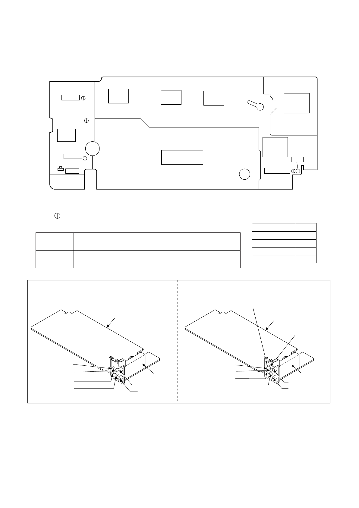
Test Point
TP301
TP501
TP507
Mechanical Alignment Procedures
Mechanical Alignment Procedures
Preparation for Servicing
Used in: Page No.
AUDIO
BLOCK
2-3-3, 2-3-4
2-3-3, 2-3-4
1-5-1
POWER
SUPPLY
BLOCK
POWER
CTL
BLOCK
TP507
SENS-INH
Comparison Chart of
Models and Marks
Model Mark
VR340/55
VR340/75
VR740/55
VR740/75
TP501
CTL
A
B
C
D
[ A, B ] [ C, D ]
Main CBA
Audio Out
Audio Out (R)
Audio In
Video Out
Video In
Tuner Unit
Antenna In
Antenna Out
Audio In (R)
Video Out
Video In
Audio Out (L)
Main CBA
Audio In (L)
Tuner Un
Antenna In
Antenna Out
1-9-2 HE274EA
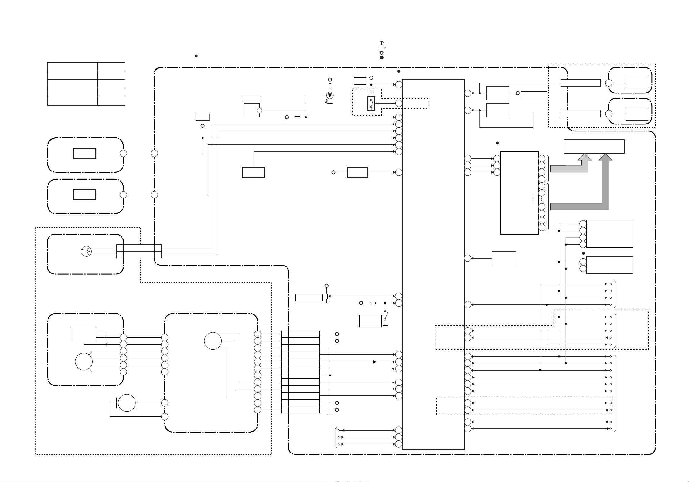
Servo/System Control Block Diagram
Comparison Chart of
Models & Marks
Model Mark
VR340/55
VR340/75
VR740/55
VR740/75 D
Q504
ST-S
SENSOR CBA
Q505
END-S
A
B
C
" " = SMD
MAIN CBA
TP505
ST-S
BLOCK DIAGRAMS
NOTE FOR WIRE CONNECTORS:
1. PREFIX SYMBOL "CN" MEANS CONNECTOR.
(CAN DISCONNECT AND RECONNECT.)
2. PREFIX SYMBOL "CL" MEANS WIRE-SOLDER
HOLES OF THE PCB.
(WIRE IS SOLDERED DIRECTLY.)
AL+5V
SW507
LD-SW
AL+5V
Q503
T-REEL
D502
S-LED
TIMER+5V
C,D
TP501
CTL
Q502
RESET
Q501
TEST POINT INFORMATION
:INDICATES A TEST POINT WITH A JUMPER WIRE ACROSS A HOLE IN THE PCB.
:USED TO INDICATE A TEST POINT WITH A COMPONENT LEAD ON FOIL SIDE.
:USED TO INDICATE A TEST POINT WITH NO TEST PIN.
:USED TO INDICATE A TEST POINT WITH A TEST PIN.
IC501
(SERVO/SYSTEM CONTROL)
97
CTL AMP OUT
FF/REW-L84
LD-SW9
95
CTL(+)
CTL(-)
94
10
ST-S
4
END-S
T-REEL
80
RESET
34
KEY- 1
KEY- 2
DRV-DATA
DRV-STB
DRV-CLK
68
69
70
C,D
CL509
7
8
KEY
SWITCH
KEY
SWITCH
IC561
(LED DISPLAY)
DRV-DATA
28
DRV-STB
2
DRV-CLK
1
TP507
SENS-INH
G1
23
G2
22
G3
21
G4
20
S1
7
S2
8
1 POWER
CL511
1 STOP/EJECT
FP562
LED DISPLAY
SW1 CBA
KEY
SWITCH
SW2 CBA
KEY
SWITCH
SENSOR CBA
(DECK ASSEMBLY)
CONTROL
HEAD
AC HEAD ASSEMBLY
CYLINDER ASSEMBLY CAPSTAN MOTOR
PG
SENSOR
DRUM
MOTOR
M
LOADING
MOTOR
CL287
5 5CTL(+)
6 6CTL(-)
M
CL504
CAPSTAN
MOTOR
M
VR501
SW-POINT
CL502
12 AL+15V
11
AL+12V(2)
10 GND
D-PFG
9
D-CONT
8
LM-FWD/REV
7
GND
6
C-CONT
5
C-F/R
4
C-FG
3
AL+5V
2
AL+12V
1
AL+5V
FROM/TO
POWER
SUPPLY
BLOCK
AL+5V
AL+15V
AL+12V
AL+5V
AL+12V
P-ON-L
P-DOWN-L
P-OFF-H
SW506
REC-
SAFETY
PG-DELAY
2
31
RECSAF-SW
D-PFG
90
D-CONT77
LM-
81
FWD/REV
C-CONT
76
C-F/R
78
C-FG
87
P-ON-L
67
P-DOWN-L
86
P-OFF-H
73
REMOCON-IN
A-MUTE-H
C,D
Hi-Fi-H-SW
A-MODE
IIC-BUS SDA
IIC-BUS SCL
D-REC-H
C-ROTA
D-V SYNC
H-A-SW
H-A-COMP
C,D
C-SYNC
RF-SW
V-ENV
14
83
19
32
72
71
33
18
15
13
16
17
58
S7
13
S8
14
S9
16
S10
17
RS501
REMOTE
SENSOR
6
TU701(TUNER UNIT)
SDA
3
SDA
12
SCL
5
SCL
11
IC503 (MEMORY)
SDA
5
SCL
6
D-REC-H
IIC-BUS SDA
IIC-BUS SCL
A-MUTE-H
IIC-BUS SDA
IIC-BUS SCL
Hi-Fi-H-SW
A-MODE
A-MUTE-H
IIC-BUS SDA
IIC-BUS SCL
D-REC-H
RF-SW
C-ROTA
D-V SYNC
H-A-SW
H-A-COMP
V-ENV
C-SYNC
TO
AUDIO BLOCK
FROM/TO
Hi-Fi AUDIO
BLOCK
FROM/TO
VIDEO BLOCK
1-10-1 1-10-2 HE274BLS
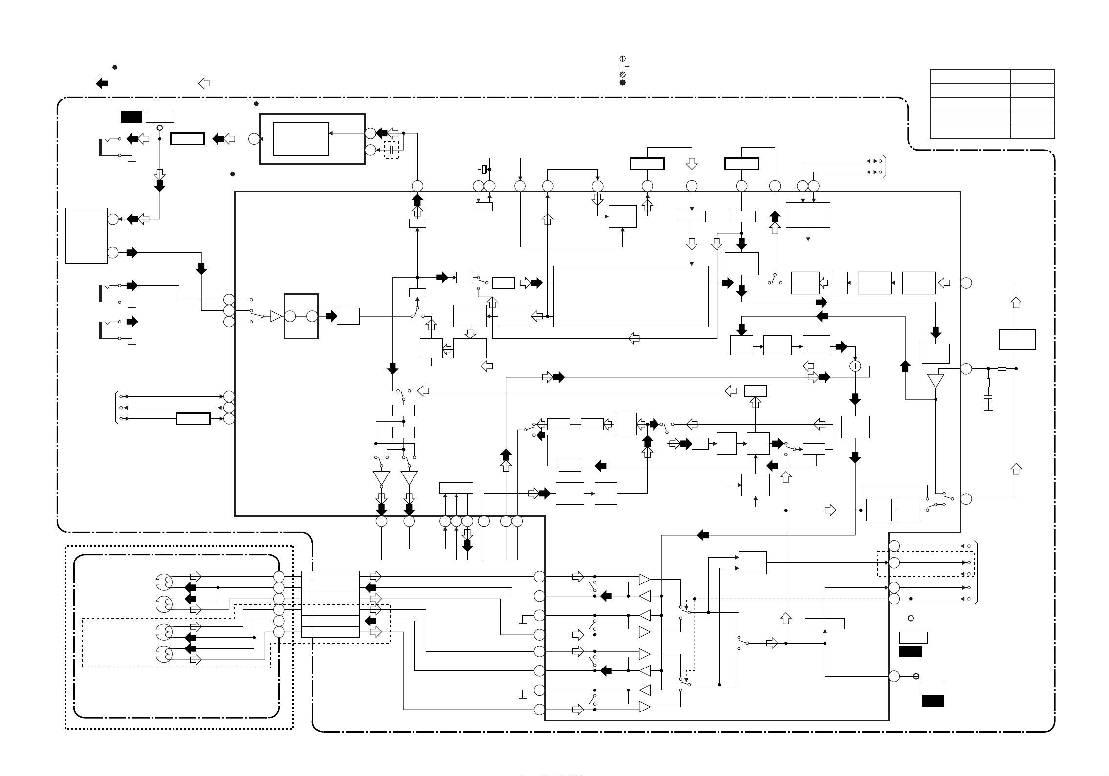
Video Block Diagram
" " = SMD
REC-VIDEO SIGNAL PB-VIDEO SIGNAL MODE: SP/REC
TP751
V-OUT
WF1
JK751
V-OUT
TU701
VIDEO
6
BUFFER
Q305
IC501 (OSD)
OSD
CHARACTER
52
MIX
IC301
(Y/C PROCESS)
COLOR
-IN
50
55
NOTE FOR WIRE CONNECTORS:
1. PREFIX SYMBOL "CN" MEANS CONNECTOR.
(CAN DISCONNECT AND RECONNECT.)
2. PREFIX SYMBOL "CL" MEANS WIRE-SOLDER
HOLES OF THE PCB.
(WIRE IS SOLDERED DIRECTLY.)
MAIN CBA
A,C
29 67 66 49
AMP
X302
4.43MHz
VXO
43
TEST POINT INFORMATION
:INDICATES A TEST POINT WITH A JUMPER WIRE ACROSS A HOLE IN THE PCB.
:USED TO INDICATE A TEST POINT WITH A COMPONENT LEAD ON FOIL SIDE.
:USED TO INDICATE A TEST POINT WITH NO TEST PIN.
:USED TO INDICATE A TEST POINT WITH A TEST PIN.
Q307
BUFFER
45
CCD 1H
DELAY
46 41
CLAMP
Q304
BUFFER
CLAMP
21 24 2320
SERIAL
DECORDER
IIC-BUS SDA
IIC-BUS SCL
Comparison Chart of
Models & Marks
FROM/TO
SERVO/SYSTEM
CONTROL BLOCK
Model Mark
VR340/55
VR340/75
VR740/55
VR740/75 D
A
B
C
TU-VIDEO
JK753
V-IN-F
JK752
V-IN
FROM/TO
SERVO
/SYSTEM
CONTROL
BLOCK
24
D-REC-H
C-SYNC
D-V SYNC
BUFFER
Q308
34
TUNER
36
38
LINE
D-REC-H
30
C-SYNC
28
D-V SYNC
27
32 31
EE
AGC
R P
BPF
D.E.
FBC
R P
R
1/2
NOISE
CANCELMDE EMPA
Y/C
MIX
PIC-CTL
ANR
C-COMB COMB
Y-LPF
P
P
R
72715759 54 52 51 61
KIL
AMP
DOC YNR Y/C COMB
MAPBPF
KILL
B.D.
CCD
LPF
R P
ACC
4.43MHz
B-UP
AMP
DETAIL
ENH
W/D
CLIP
CONV
629KHz
BPF
MAIN
CONV
SUB
R P
FM
MOD
R
P
V/I
CONV
FM-EQ
C-LPF
REC
SUB
LPF
REC FM
AGC
FM
DEMOD.
PB FM
AGC
DOUBLE
LIMIT
PB
FM-EQ
NL
EMPHA
R
P
17
Q302, Q303
19
18
PEAKING
AMP
(DECK ASSEMBLY)
CYLINDER ASSEMBLY
VIDEO (R)-1 HEAD
VIDEO (L)-1 HEAD
VIDEO (L)-2 HEAD
VIDEO (R)-2 HEAD
C,D
WF2
C-ROTA
H-A-COMP
H-A-SW
V-ENV
RF-SW
TP301
C-PB
FROM/TO
SERVO/SYSTEM
CONTROL BLOCK
1
2
3
4
5
6
CL253
V(R)-1
V-COM
V(L)-1
V(L)-2
V-COM
V(R)-2
91
90
89
88
85
84
83
C-ROTA
COMP
OUT
10
94
C,D
93
11
R
L
SP
ENV DET
TP502
RF-SW
EP
L
74
R
WF3
82
1-10-3 1-10-4 HE274BLV

Audio Block Diagram
NOTE FOR WIRE CONNECTORS:
" " = SMD
REAR
TU701
A-OUT (L)
A,B
A-OUT
A-OUT (R)
C,D
A,B
A-IN
C,D
A-IN (L)
A-IN (R)
A-IN (L)-F
AUDIO OUT
1. PREFIX SYMBOL "CN" MEANS CONNECTOR.
(CAN DISCONNECT AND RECONNECT.)
2. PREFIX SYMBOL "CL" MEANS WIRE-SOLDER
HOLES OF THE PCB.
(WIRE IS SOLDERED DIRECTLY.)
SIF OUT
AUDIO IN
15
2
2
JK751
JK752
JK754
CN701 CN1
TP754
A-OUT(L)
SIF
TP752
A-OUT(R)
TEST POINT INFORMATION
:INDICATES A TEST POINT WITH A JUMPER WIRE ACROSS A HOLE IN THE PCB.
:USED TO INDICATE A TEST POINT WITH A COMPONENT LEAD ON FOIL SIDE.
:USED TO INDICATE A TEST POINT WITH NO TEST PIN.
:USED TO INDICATE A TEST POINT WITH A TEST PIN.
AFV CBA
22
IF SIGNAL
PROCESS
4
TU-AUDIO(R)
TU-AUDIO(L)
5
Comparison Chart of
Models & Marks
Model Mark
VR340/55
VR340/75
VR740/55
PB-AUDIO SIGNAL REC-AUDIO SIGNAL Mode : SP/REC
VR740/75 D
MAIN CBA
CN701CN1
4
5
J928
J919
IC301
(AUDIO PROCESS)
J917
C,D
TUNER LINE
78
A,B
J916
76
A,B
J926
TU-AUDIO(R)
TU-AUDIO(L)
MOD-A
A-IN (L)
A-IN (R)
A-IN (L)-F
A-IN (R)-F
A-OUT (L)
A-OUT (R)
N-A-REC
N-A-PB
J918J24
A
B
C
FROM/TO
Hi-Fi AUDIO
BLOCK
C,D
FRONT
A-IN (R)-F
(DECK ASSEMBLY)
AUDIO
HEAD
AUDIO
ERASE
HEAD
FULL
ERASE
HEAD
JK755
C,D
ACE HEAD ASSEMBLY
CN287
A-PB/REC 4
A-COM 3
AE-H 1
AE-H/FE-H 2
FE HEAD
CL504
4 A-PB/REC
3 A-COM
1 AE-H
2 AE-H/FE-H
CL501
2 FE-H
1 FE-H-GND
Q402
BIAS
OSC
Q404
(PB=ON)
Q405
(PB=ON)
Q403
4
3
99
Q401
AL+5V
SWITCHING
D-REC-OFF
AL+5V
PB-ON
EQ
AMP
SP/LP-ON
AUTO
BIAS
ALC
R
1
2
100
P
76
REC
AMP
LINE
AMP
10
MUTE
SERIAL
DECODER
23 24
96
98
IIC-BUS SDA
IIC-BUS SCL
A-MUTE-H
D-REC-H
TO SERVO/SYSTEM
CONTROL BLOCK
1-10-5 1-10-6 HE274BLA
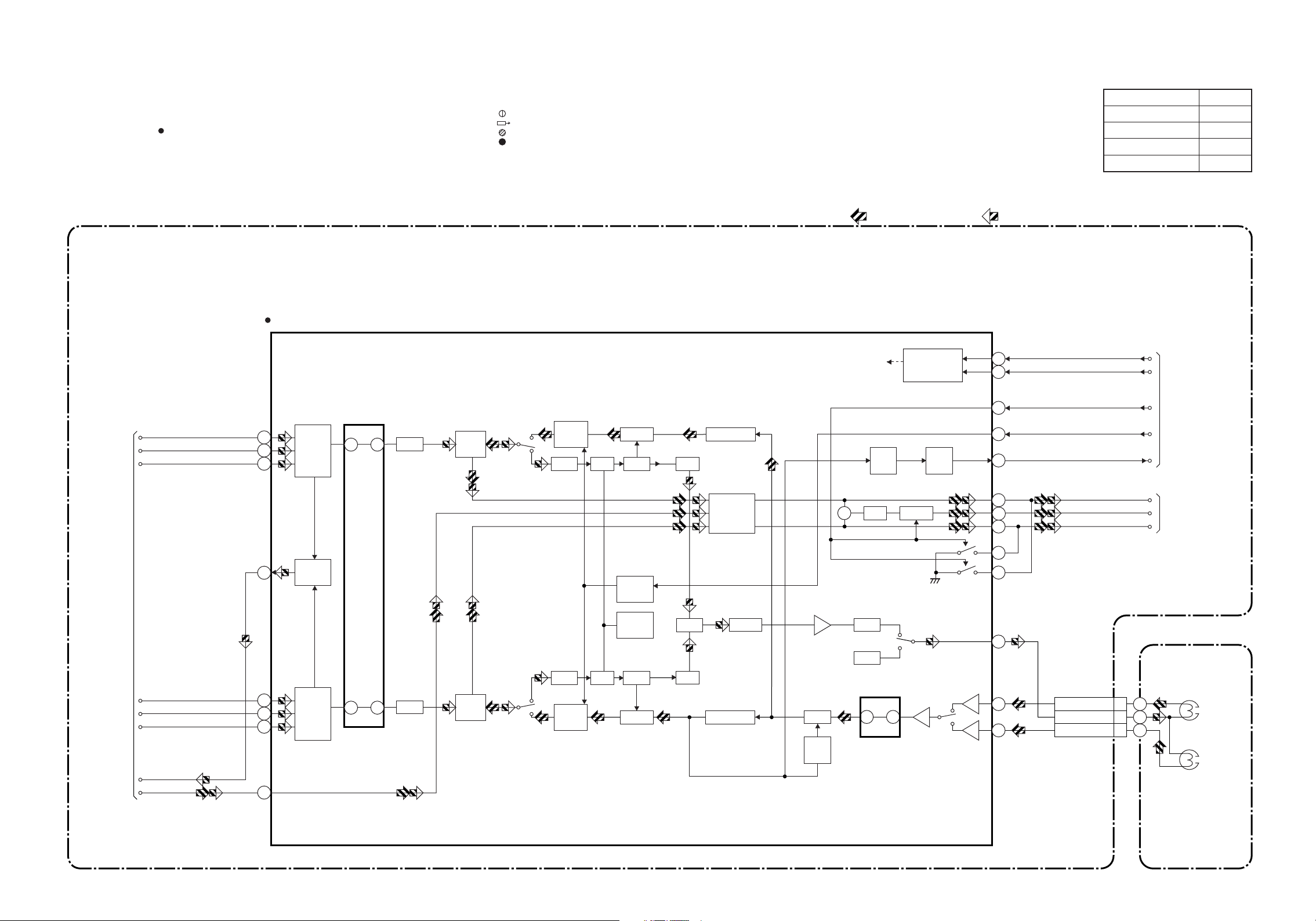
Hi-Fi Audio Block Diagram ( C, D )
NOTE FOR WIRE CONNECTORS:
1. PREFIX SYMBOL "CN" MEANS CONNECTOR.
(CAN DISCONNECT AND RECONNECT.)
" " = SMD
2. PREFIX SYMBOL "CL" MEANS WIRE-SOLDER
HOLES OF THE PCB.
(WIRE IS SOLDERED DIRECTLY.)
IC451 (MTS/ SAP/ Hi-Fi AUDIO PROCESS/ Hi-Fi HEAD AMP)
TEST POINT INFORMATION
:INDICATES A TEST POINT WITH A JUMPER WIRE ACROSS A HOLE IN THE PCB.
:USED TO INDICATE A TEST POINT WITH A COMPONENT LEAD ON FOIL SIDE.
:USED TO INDICATE A TEST POINT WITH NO TEST PIN.
:USED TO INDICATE A TEST POINT WITH A TEST PIN.
MAIN CBA
Comparison Chart of
Models & Marks
Model Mark
VR340/55
VR340/75
VR740/55
VR740/75 D
REC-AUDIO SIGNALPB-AUDIO SIGNAL Mode : SP/REC
A
B
C
TO AUDIO
BLOCK
A-IN(R)
TU-AUDIO(R)
A-IN(R)-F
A-IN(L)
TU-AUDIO(L)
A-IN(L)-F
N-A-REC
N-A-PB
52
44
49
53
61
63
54
SERIAL
DATA
DECODER
R-CH
INSEL
NOR
SW
L-CH
6
INSEL
46 45
4 5
ALC
ALC
R-CH
PNR
L-CH
PNR
P
R
R
P
SW
NOISE
LIM DEV
LIM DEV
SW
NOISE
COMP
VCO
HOLD
PULSE
NOISE
DET
VCO
COMP
LPF
MIX
LPF
R-CH BPF
OUTPUT
SELECT
COMP AMP
L-CH BPF
AGC
AGC
DET
+
ALC MUTE
BIAS
18 19
OD
DET
ENV
DET
R
P
R
L
31
32
8
35
17
58
57
56
55
59
26
22
25
IIC-BUS SDA
IIC-BUS SCL
A-MUTE-H
Hi-Fi-SW
A-MODE
A-OUT(L)
MOD-A
A-OUT(R)
CN253
Hi-Fi-A(R) 7
Hi-Fi-COM 8
Hi-Fi-A(L) 9
FROM/TO
SERVO/ SYSTEM
CONTROL BLOCK
TO
AUDIO BLOCK
Hi-Fi
AUDIO
(R) HEAD
Hi-Fi
AUDIO
(L) HEAD
CYLINDER
ASSEMBLY
HE494BLH1-10-7 1-10-8
Power Supply Block Diagram
Comparison Chart of
Models & Marks
Model Mark
VR340/55
VR340/75
VR740/55
VR740/75 D
A
B
C
AC001
NOTE :
The voltage for parts in hot circuit is measured using
hot GND as a common terminal.
HOT CIRCUIT. BE CAREFUL.
F001
T1.6A L 250V
L003
LINE
FILTER
D001 - D004
BRIDGE
RECTIFIER
CAUTION
FOR CONTINUED PROTECTION AGAINST FIRE HAZARD,
REPLACE ONLY WITH THE SAME TYPE T1.6AL/250V FUSE.
T001
2
4
Q001
12
13
Q059
14
15
16
C,D
CAUTION !
Fixed voltage (or Auto voltage selectable ) power supply circuit is used in this unit.
If Main Fuse (F001) is blown, check to see that all components in the power supply
circuit are not defective before you connect the AC plug to the AC power supply.
Otherwise it may cause some components in the power supply circuit to fail.
MAIN CBA
AL+15V
AL+32V
P-ON-L
AL+12V
P-ON+9V
Q053
C,D
Q054
C,D
AL+5V
P-ON+5V
TIMER+5V
P-DOWN-L
P-OFF-H
Q003
HOT
Q002
7
6
IC001
ERROR
VOLTAGE DET
4
Q004
SHUNT
REGULATOR
1
23
REG
11
Q055
Q056
17
Q057
18
COLD
1-10-9 1-10-10
HE274BLP
(
e
SCHEMATIC DIAGRAMS / CBA'S AND TEST POINTS
1
Standard Notes
WARNING
Notes:
1. Do not use the part n umber shown on thes e drawings for ordering. The correct part number is
Many electrical and mechanical parts in this chassis
have special characteristics. These characteristics
often pass unnoticed and the protection afforded by
them cannot nece ssar ily b e ob tai ned by us ing repl ac ement components rated for higher voltage, wattage,
etc. Replacement parts that have th ese spe cial safety
characteristics are identified in this manual and its
supplements; electrical comp onents having such features are identified by the mark " ! " in the schematic
diagram and the parts list. Before replacing any of
these components, read the parts list in this manual
carefully. The use of substitute replacement parts that
do not have the same s afety character istics as specified in the parts list may create shock, fire, or other
hazards.
Capacitor Temperature Markings
Mark
(B)
Capacity
change rate
±10%
Standard
Temperature
temperature
20°C -25~+85°C
range
(F) +30 - 80% 20°C –25~+85°C
(SR)
±15%
20°C –25~+85°C
shown in the parts list, and may be slightly different
or amended since these drawings were prepared.
2. To maintain original function and reliability of
repaired units, use onl y original replace ment parts
which are listed with the ir part numb ers i n the parts
list section of the service manual.
3. Prefix symbol "CN" means "connector" (can disconnect and reconnect).
Prefix symbol "CL" m ean s " wir e-s old er hol es of the
PCB" (wire is soldered directly).
4. How to read converged lines.
-D3
Distinction Area
Line Number
(1 to 3 digits)
Examples:
3
AREA D3
2
1
AREA B1
1-D3
ABCD
1-B1
(1). "1-D3" means that line number "1" goes to
area "D3."
(2). "1-B1" means that line number "1" goes to
area "B1."
5. All resistance values are indicated in ohms
(Y)
±22.5%
Capacitors and transistor s are represented by the following symbols.
20°C –25~+85°C
3
(K=10
, M=106).
6. Resis tor wattages a re 1/4 W or 1/6W u nless other wise specified.
7. All capacitance values are indicated in µF
-6
(P=10
µF).
8. All voltages are DC voltages unless otherwise
specified.
9. Voltage indications for PLAY and REC modes on
the schematics are as shown below.
< PCB Symbols >
(Top View) (Bottom View)
2
+
Electrolytic Capacitor
Bottom View)
Transistor or Digital Transistor
E C B
(Top View)
NPN Transistor
(Top View)
PNP Transistor
(Unit: Volt)
The same voltage for
both PLAY & REC modes.
1
5.0
< Schematic Diagram Symbols >
3
5.0
(2.5)
Indicates that the voltage
is not consistent here.
Digital Transistor
PLAY mod
REC mode
E C B
(Top View)
NPN Digital Transistor
E C B
E C B
(Top View)
PNP Digital
Transistor
E C B
1-11-1 SC_08
 Loading...