Philips UOCIII-v2.0 Service Manual

INTEGRATED CIRCUITS
DEVICE SPECIFICATION
DATA SH EET
UOC
III
series
Versatile signal processor for lowand mid-range TV applications
Preliminary specification
File under Integrated Circuits, <Handbook>
Version: 2.0
CONFIDENTIAL
Previous date: 2003 Nov 11
2003 Dec 18

Philips Semiconductors Preliminary specification
Versatile signal processor for low- and
mid-range TV applications
GENERAL DESCRIPTION
The UOC
SignalProcessor(VSP)togetherwithaFLASHembedded
TEXT/Control/Graphics µ-Controller (TCG µ-Controller)
and US Closed Caption decoder. In addition the following
functions can be added:
• Adaptive digital (4H/2H) PAL/NTSC combfilter
• Teletext decoder with 10 page text memory
• Multi-standard stereo decoder
• BTSC stereo decoder
• Digital sound processing circuit
• Digital video processing circuit
The UOC
concepts:
• Stereo versions. These versions contain the TV
processor with a stereo audio selector, the TCG
µ-Controller, the multi-standard stereo or BTSC
decoder, the digital sound processing circuit and the
digital video processing circuit. Options arethe adaptive
digitalPAL/NTSCcombfilterand a teletext decoder with
10 page text memory.
• AV stereo versions. These versions contain the TV
processor with stereo audio selector and the TCG
µ-Controller. Options are the digital sound processing
circuit, the digital video processing circuit, the adaptive
digitalPAL/NTSCcombfilterand a teletext decoder with
a 10 page text memory.
• Mono sound versions. These versions contain the TV
processorwithaselectorformonoaudiosignalsandthe
TCG µ-Controller. Options are the adaptive digital
PAL/NTSC combfilter and a teletext decoder with 10
page text memory.
The most important features of the complete IC series are
given in the following feature lists. The exact feature
content of the various ICs is given in Table 1 on page 7.
TheICsaremountedinaQFP-128envelope
used in economy television receivers with 90° and 110°
picture tubes. They have supply voltages of 5V, 3.3V. Also
an 1.8V supply is needed, but this can be simply derived
by adding an emitter follower at a reference voltage from
the device.
UOC
Software Development kit to enable easy programming
and fast time-to-market (see also Chapter “LICENSE
INFORMATION” on page 6.
III
series combines the functions of a Video
III
series consists of the following 3 basic
(1)
III
is supported by a comprehensive Global TV
andcanbe
III
UOC
FEATURES
Analogue Video Processing (all versions)
• Multi-standard vision IF circuit with alignment-free PLL
demodulator
• Internal (switchable) time-constant for the IF-AGC circuit
• Switchable group delay correction and sound trap (with
switchablecentrefrequency)forthedemodulated CVBS
signal
• DVB/VSB IF circuit for preprocessing of digital TV
signals.
• Video switch with 3 external CVBS inputs and a CVBS
output. All CVBS inputs can be used as Y-input for Y/C
signals. However, only 2 Y/C sources can be selected
because the circuit has 2 chroma inputs. It is possible to
add an additional CVBS(Y)/C input (CVBS/YX and CX)
when the YUV interface and the RGB/YPRPB input are
not needed.
• Automatic Y/C signal detector
• Adaptive digital (4H/2H) PAL/NTSC comb filter for
optimum separation of the luminance and the
chrominance signal.
• Integrated luminance delay line with adjustable delay
time
• Picture improvement features with peaking (with
switchable centre frequency, depeaking, variable
positive/negative peak ratio, variable pre-/overshoot
ratio and video dependent coring), dynamic skin tone
control, gamma control and blue- and black stretching.
All features are available for CVBS, Y/C and
RGB/YPBPR signals.
• Switchable DC transfer ratio for the luminance signal
• Only one reference (24.576 MHz) crystal required for
the TCG µ-Controller, digital sound processor, Teletextand the colour decoder
• Multi-standard colour decoder with automatic search
system and various “forced mode” possibilities
• Internal base-band delay line
series
(1) Both standard and “face down” versions of the QFP128
0.8mm pitch package are available.
2003 Dec 18 2
CONFIDENTIAL

Philips Semiconductors Preliminary specification
Versatile signal processor for low- and
mid-range TV applications
• Indication of the Signal-to-Noise ratio of the incoming
CVBS signal
• Linear RGB/YPBPR input with fast insertion.
• YUV interface. When this feature is not required some
pins can be used as additional RGB/YPBPR input. It is
also possible to use these pins for additional CVBS (or
Y/C) input (CVBS/YX and CX).
• Tint control for external RGB/YPBPR signals
• Scan Velocity Modulation output. The SVM circuit is
active for all the incoming CVBS, Y/C and RGB/YPBP
signals. The SVM function can also be used during the
display of teletext pages.
• RGB control circuit with ‘Continuous Cathode
Calibration’, white point and black level off-set
adjustment so that the colour temperature of the dark
and the light parts of the screen can be chosen
independently.
• Contrast reduction possibility during mixed-mode of
OSD and Text signals
• Adjustable ‘wide blanking’ of the RGB outputs
• Horizontal synchronization with two control loops and
alignment-free horizontal oscillator
• Vertical count-down circuit
• Vertical driver optimized for DC-coupled vertical output
stages
• Horizontal and vertical geometry processing with
horizontal parallelogram and bow correction and
horizontal and vertical zoom
• Low-power start-up of the horizontal drive circuit
Analogue video processing (stereo versions)
• The low-pass filtered ‘mixed down’ I signal is available
via a single ended or balanced output stage.
Analogue video processing (mono versions)
• The low-pass filtered ‘mixed down’ I signal is available
via a single ended output stage
Digital Video Processing (some versions)
• Double Window mode applications. It is possible to
display a video and a text window or 2 text windows in
parallel.
• Linear and non-linear horizontal scaling of the video
signal to be displayed.
UOC
Sound Demodulation (all versions)
• Separate SIF (Sound IF) input for single reference QSS
(Quasi Split Sound) demodulation.
• AM demodulator without extra reference circuit
• The mono intercarrier sound circuit has a selective
FM-PLL demodulator which can be switched to the
different FM sound frequencies (4.5/5.5/6.0/6.5 MHz).
The quality of this system is such that the external
band-pass filters can be omitted. In the stereo versions
R
of UOC
special applications. Normally the FM demodulators of
the stereo demodulator/decoder part are used (see
below).
• The FM-PLL demodulator can be set to centre
frequencies of 4.72/5.74 MHz so that a second sound
channel can be demodulated. In such an application it is
necessary that an external bandpass filter is inserted.
• The vision IF and mono intercarrier sound circuit can be
used for the demodulation of FM radio signals. With an
external FM tuner also signals with an IF frequency of
10.7 MHz can be demodulated.
• Switch to select between 2nd SIF from QSS
demodulation or external FM (SSIF)
Audio Interfaces and switching (stereo versions with
Audio DSP)
• Audio switch circuit with 4 stereo inputs, a stereo output
for SCART/CINCH, 1 stereo output for HEADPHONE.
The headphone channel has an analogue volume
control circuit for the L and R channel. Finally 1 stereo
SPEAKER output with digital controls.
• AVL (Automatic Volume Levelling) circuit for the
headphone channel.
• Digital input crossbar switch for all digital signal sources
and destinations
• Digital output crossbar for exchange of channel
processing functionality
• Digital audio input interface (stereo I2S input interface)
• Digital audio output interface (stereo I2S output
interface)
Audio interfaces and switching (AV stereo versions
without Audio DSP)
• Audio switch circuit with 4 stereo inputs, a stereo output
for SCART/CINCH and a stereo SPEAKER output with
analogue volume control.
• Analogue mono AVL circuit at left audio channel
III
the use of this demodulator is optional for
III
series
2003 Dec 18 3
CONFIDENTIAL

Philips Semiconductors Preliminary specification
Versatile signal processor for low- and
mid-range TV applications
Audio interfaces and switching (mono versions)
• Audio switch circuit with 4 external audio (mono) inputs
and a volume controlled output
• AVL circuit
Stereo Demodulator and Decoder (full stereo
versions)
• Demodulator and Decoder Easy Programming (DDEP)
• Auto standard detection (ASD)
• Static Standard Selection (SSS)
• DQPSK demodulation for different standards,
simultaneously with 1-channel FM demodulation
• NICAM decoding (B/G, I, D/K and L standard)
• Two-carrier multistandard FM demodulation (B/G, D/K
and M standard)
• Decoding for three analog multi-channel systems (A2,
A2+ and A2*) and satellite sound
• Adaptive de-emphasis for satellite FM
• OptionalAMdemodulationforsystem L, simultaneously
with NICAM
• Identification A2 systems (B/G, D/K and M standard)
with different identification time constants
• FM pilot carrier present detector
• Monitor selection for FM/AM DC values and signals,
with peak and quasi peak detection option
• BTSC MPX decoder
• SAP decoder
• dbx® noise reduction
• Japan (EIAJ) decoder
• FM radio decoder
• Soft-mute for DEMDEC outputs DEC, MONO and SAP
• FM overmodulation adaptation option to avoid clipping
and distortion
Audio Multi Channel Decoder (stereo versions with
Audio DSP)
• Dolby® Pro Logic® (DPL)
• Five channel processing for Main Left and Right,
Subwoofer,Centre and Surround. To exploit this feature
an external DAC is required.
(1) Dolby is a trademark of Dolby Laboratories
(4)
(1)
III
UOC
series
Volume and tone control for loudspeakers (stereo
versions with Audio DSP)
• Automatic Volume Level (AVL) control
• Smooth volume control
• Master volume control
• Soft-mute
• Loudness
• Bass, Treble
• Dynamic Bass Boost (DBB)
• Dynamic Virtual Bass (DVB)
• BBE® Sound processing
(2)
(3)
(4)
• Graphic equaliser
• Processed or non processed subwoofer
• Programmable beeper
Reflection and delay for loudspeaker channels
(stereo versions with Audio DSP)
• Dolby® Pro Logic® Delay
(1)
• Pseudo hall/matrix function
Psycho acoustic spatial algorithms, downmix and
split in loudspeaker channels (stereo versions with
Audio DSP)
• Extended Pseudo Stereo (EPS)
• Extended Spatial Stereo (ESS)
• Virtual Dolby® Surround (VDS 422,423)
• SRS 3D and SRS TruSurround®
(5)
(6)
(1)
(4)
RDS/RBDS
• Demodulation of the European Radio Data system
(RDS) or the USA Radio Broadcast Data System
(RBDS) signal
• RDS and RBDS block detection
• Error detection and correction
• Fast block synchronisation
• Synchronisation control (flywheel)
• Mode control for RDS/RBDS processing
• Different RDS/RBDS block information output modes
(2) Also referred to as “Dynamic UltraBass”
(3) Also referred to as “Dynamic Bass Enhancement”
(4) For the use of these products a licence is required. More
details are given in the chapter “LICENSE INFORMATION”on
page 6
(5) Also referred to as “I-Mono” or “Incredible Mono”
(6) Also referred to as “I-Stereo” or “Incredible Stereo”
2003 Dec 18 4
CONFIDENTIAL

Philips Semiconductors Preliminary specification
Versatile signal processor for low- and
mid-range TV applications
µ-Controller
• 80C51 µ-controller core standard instruction set and
timing
• 0.4883 µs machine cycle
• maximum of 256k x 8-bit flash programmable ROM
• maximum of 8k x 8-bit Auxiliary RAM
• 12-level Interrupt controller for individual enable/disable
with two level priority
• Two 16-bit Timer/Counter registers
• One 24-bit Timer (16-bit timer with 8-bit Pre-scaler)
• WatchDog timer
• Auxiliary RAM page pointer
• 16-bit Data pointer
• Stand-by, Idle and Power Down modes
• 24 general-purpose I/O pins
• 14 bits PWM for Voltage Synthesis Tuning
• 8-bit A/D converter with 4 multiplexed inputs
• 5 PWM (6-bits) outputs for analogue control functions
• Remote Control Pre-processor (RCP)
• Universal Asynchronous Receiver Transmitter (UART)
Data Capture
• Text memory up to 10 pages
• Inventory of transmitted Teletext pages stored in the
Transmitted Page Table (TPT) and Subtitle Page Table
(SPT)
• Data Capture for US Closed Caption
• Data Capture for 525/625 line WST, VPS (PDC system
A) and 625 line Wide Screen Signalling (WSS) bit
decoding
• Automatic selection between 525 WST/625 WST
• Automatic selection between 625 WST/VPS on line 16
of VBI
• Real-time capture and decoding for WST Teletext in
Hardware, to enable optimized µ-processor throughput
• Automatic detection of FASTEXT transmission
• Real-time packet 26 engine in Hardware for processing
accented, G2 and G3 characters
• Signal quality detector for video and WST/VPS data
types
• Comprehensive teletext language coverage
• Vertical Blanking Interval (VBI) data capture of WST
data
III
UOC
Display
• Teletext and Enhanced OSD modes
• Features of level 1.5 WST and US Close Caption
• 50Hz/60Hz display timing modes
• Two page operation for 16:9 screens
• Serial and Parallel Display Attributes
• Single/Double/Quadruple Width and Height for
characters
• Smoothingcapability of both Double Size, Double Width
& Double Height characters
• Scrolling of display region
• Variable flash rate controlled by software
• Soft colours using CLUT with 4096 colour palette
• Globally selectable scan lines per row (9/10/13/16/) and
character matrix [12x9, 12x13, 12x16, 16x18, (VxH)]
• Fringing (Shadow) selectable from N-S-E-W direction
• Fringe colour selectable
• Contrast reduction of defined area
• Cursor
• Special Graphics Characters with two planes, allowing
four colours per character
• 64 software redefinable On-Screen display characters
• 4 WST Character sets (G0/G2) in single device (e.g.
Latin, Cyrillic, Greek, Arabic)
• G1 Mosaic graphics, Limited G3 Line drawing
characters
• WST Character sets and Closed Caption Character set
in single device
• SVM for Text
series
2003 Dec 18 5
CONFIDENTIAL

Philips Semiconductors Preliminary specification
Versatile signal processor for low- and
mid-range TV applications
LICENSE INFORMATION
dbx
dbx is a registered trademark of Carillon Electronics Corp. A license is required for the use of this product. For further
information, please contact THAT Corporation, 45 Summer street, Milford, Massachusetts 01757-1656, USA.
Tel: 1-508-478-9200, FAX: 1-508-478-0990
Dolby
“Dolby”, “Pro Logic” and the double-D symbol are trademarks of Dolby Laboratories, San Francisco, USA, products are
available to licensees of Dolby Laboratories Licensing Corporation, 100 Potrero Avenue, San Francisco, CA, 94103,
USA,
Tel: 1-415-558-0200, Fax: 1-415-863-1373
Supply of this Implementation of Dolby Technology does not convey a license nor imply a right under any patent, or any
other Industrial or Intellectual Property Right of Dolby Laboratories, to use this Implementation in any finished end-user
or ready-to-use final product. It is hereby notified that a license for such use is required from Dolby Laboratories.
BBE
BBE is a registered trademark of BBE Sound, Inc., 5381 Production Drive, Huntington Beach, California 92649, USA.
The use of BBE needs licensing from BBE Sound, Inc.
UOC
III
series
Tel: 1-714-897-6766, Fax: 1-714-895-6728
The SRS TruSurround technology rights incorporated in the TDA120xxH are owned by SRS Labs, a U.S. Corporation
and licensed to Philips Semiconductors B.V. Purchaser of TDA120xxH must sign a license for use of the chip and display
of the SRS Labs trademarks. Any products incorporating the TDA120xxH must be sent to SRS Labs for review. SRS
and TruSurround are protected under US and foreign patents issued and/or pending. TruSurround, SRS and (O) symbol
are trademarks of SRS Labs, Inc. in the United States and selected foreign countries. Neither the purchase of the chip
TDA120xxH, nor the corresponding sale of audio enhancement equipment conveys the right to sell commercialized
recordings made with any SRS technology. SRS Labs requires all set makers to comply with all rules and regulations as
outlined in the SRS Trademark Usage Manual separately provided.
Philips
“Dynamic Ultra BassTM”, “Dynamic Bass Enhancement”, “I-Mono” and “I-Stereo” are denominators for Philips patented
technologies. The use of the IC does not imply any copyrights nor the right to use the same denominators but instead
generic ones such as listed below.
Generic name/ Philips name
• Dynamic Virtual Bass (DVB)/Dynamic UltraBass
• Dynamic Bass Boost (DBB)/Dynamic Bass Enhancement
• Extended Pseudo Stereo (EPS)/I-Mono
• Extended Spatial Stereo (ESSI)/I-Stereo
GTV
Delivery and use of the GTV Software Development Kit requires a separate License sold by Philips Semiconductors B.V.
Please contact your nearest Philips Semiconductors sales office for further details.
2003 Dec 18 6
CONFIDENTIAL
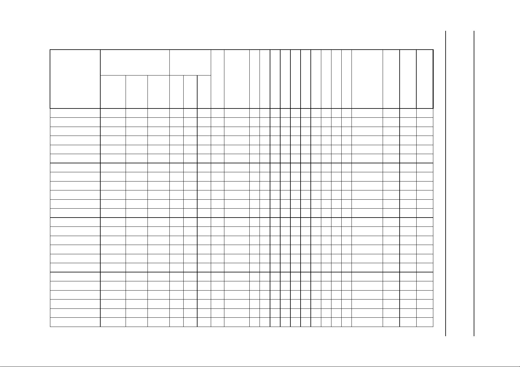
2003 Dec 18 7
OVERVIEW OF THE VARIOUS VERSIONS
Table 1 Overview of types
TYPE NUMBER
(1)
TDA11000H/H1 √√ NTSC √ 128 4 1.25 2.25
TDA11001H/H1 √√ √NTSC √ 128 4 1.25 2.25
CONFIDENTIAL
TDA11010H/H1 √√ MULTI √ 128 4 1.25 2.25
TDA11011H/H1 √√ √MULTI √ 128 4 1.25 2.25
TDA11020H/H1 √√ MULTI √ 128 4 10 2.25
TDA11021H/H1 √√√MULTI √ 128 4 10 2.25
TDA12000H/H1
TDA12001H/H1
(2)
(2)
TDA12006H/H1 BTSC
TDA12007H/H1 BTSC
TDA12008H/H1 BTSC
TDA12009H/H1 BTSC
TDA12010H/H1
TDA12011H/H1
(2)
(2)
TDA12016H/H1 MULTI √√ MULTI √√ √√√128/256 8 1.25 2.25
TDA12017H/H1 MULTI √√√MULTI √√ √√√128/256 8 1.25 2.25
TDA12018H/H1 MULTI √√ MULTI √ √√√√√√√√ 128/256 8 1.25 2.25
TDA12019H/H1 MULTI √√√MULTI √ √√√√√√√√ 128/256 8 1.25 2.25
TDA12020H/H1
TDA12021H/H1
(2)
(2)
TDA12026H/H1 MULTI √√MULTI √√ √√√128/256 8 10 2.25
TDA12027H/H1 MULTI √√√MULTI √√ √√√128/256 8 10 2.25
TDA12028H/H1 MULTI √√MULTI √ √√√√√√√√ 128/256 8 10 2.25
TDA12029H/H1 MULTI √√√MULTI √ √√√√√√√√ 128/256 8 10 2.25
COMB FILTER
COLOUR DECODER
STEREO FM RADIO
MONO FM RADIO
RDS/RBDS
dbx®
Dolby® ProLogic®
Virtual Dolby® (VDS)
SRS® 3D Stereo
SRS® TruSurround
BBETMDW / PANORAMA
ROM SIZE (k)
AUX RAM SIZE (k)
DISPLAY RAM (k)
NUMBER OF
SOUND SYSTEM
TELETEXT
PAGES
STEREO
DECO-
DER
BTSC
BTSC
AUDIO
(3)
(3)
(3)
(3)
(3)
(3)
MONO 0 10
DSP
√√ NTSC √√ 128/256 8 1.25 2.25
√√ √NTSC √√ 128/256 8 1.25 2.25
√√ NTSC √√ √√√128/256 8 1.25 2.25
√√ √NTSC √√ √√√128/256 8 1.25 2.25
√√ NTSC √ √√√√√√√√ 128/256 8 1.25 2.25
√√ √NTSC √ √√√√√√√√ 128/256 8 1.25 2.25
MULTI √√ MULTI √√ 128/256 8 1.25 2.25
MULTI √√√MULTI √√ 128/256 8 1.25 2.25
MULTI √√MULTI √√ 128/256 8 10 2.25
MULTI √√√MULTI √√ 128/256 8 10 2.25
mid-range TV applications
DRCS RAM (k)
UOC
III
series
Philips Semiconductors Preliminary specification
Versatile signal processor for low- and
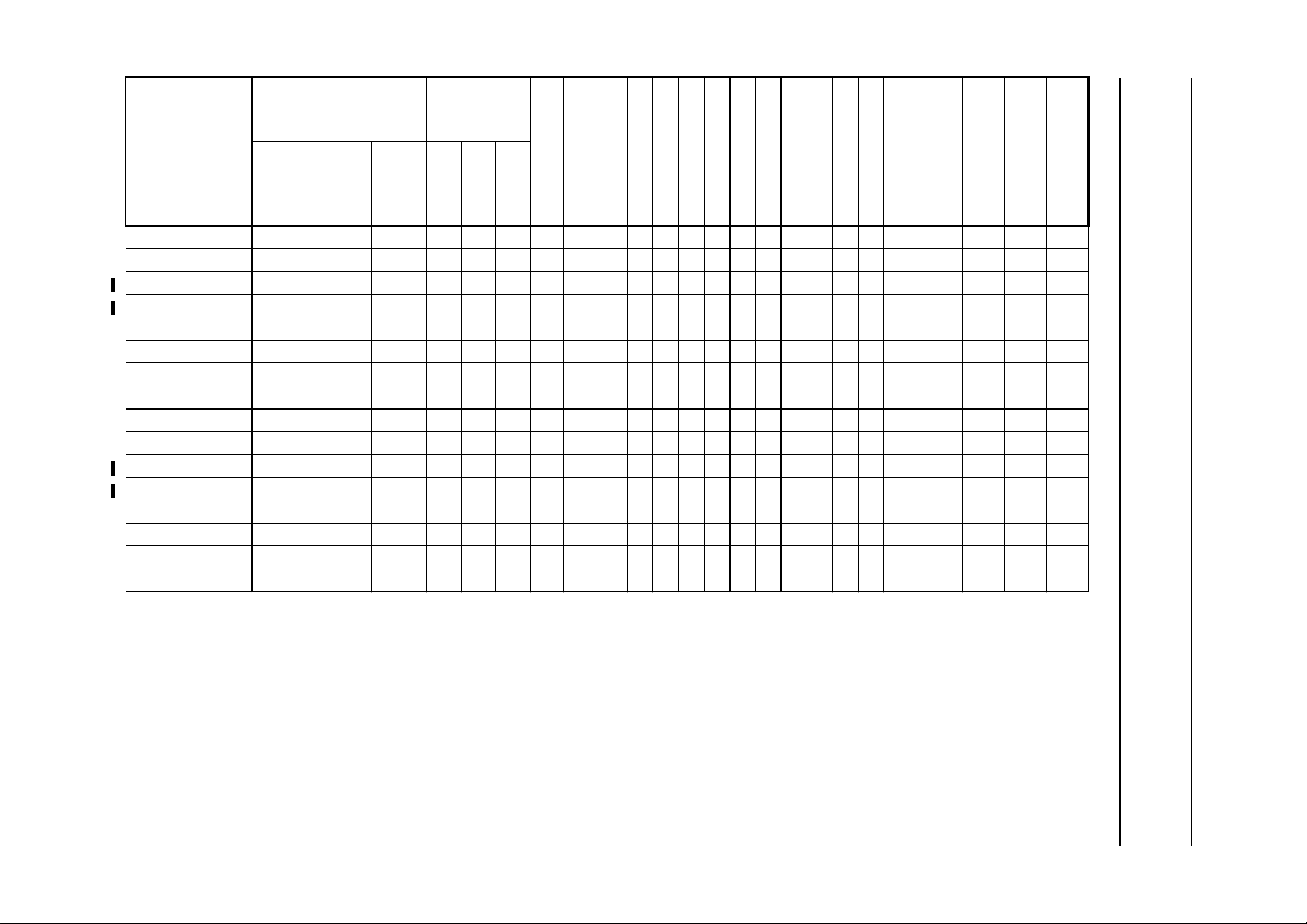
2003 Dec 18 8
TYPE NUMBER
TDA12060H/H1 √ MULTI √ 128/256 8 1.25 2.25
TDA12061H/H1 √√MULTI √ 128/256 8 1.25 2.25
TDA12062H/H1
TDA12063H/H1
CONFIDENTIAL
TDA12066H/H1 √√ MULTI √√ √ √√ 128/256 8 1.25 2.25
TDA12067H/H1 √√ √MULTI √√ √ √√ 128/256 8 1.25 2.25
TDA12068H/H1 √√ MULTI √√ √√√√√√ 128/256 8 1.25 2.25
TDA12069H/H1 √√ √MULTI √√ √√√√√√ 128/256 8 1.25 2.25
TDA12070H/H1 √ MULTI √ 128/256 8 10 2.25
TDA12071H/H1 √√MULTI √ 128/256 8 10 2.25
TDA12072H/H1
TDA12073H/H1
TDA12076H/H1 √√MULTI √√ √ √√ 128/256 8 10 2.25
TDA12077H/H1 √√√MULTI √√ √ √√ 128/256 8 10 2.25
TDA12078H/H1 √√MULTI √√ √√√√√√ 128/256 8 10 2.25
TDA12079H/H1 √√√MULTI √√ √√√√√√ 128/256 8 10 2.25
(1)
(2)
(2)
(2)
(2)
SOUND SYSTEM
STEREO
DECO-
DER
AUDIO
DSP
COMB FILTER
NUMBER OF
TELETEXT
PAGES
MONO 0 10
√√ MULTI √ 128/256 8 1.25 2.25
√√ √MULTI √ 128/256 8 1.25 2.25
√√MULTI √ 128/256 8 10 2.25
√√√MULTI √ 128/256 8 10 2.25
COLOUR DECODER
STEREO FM RADIO
MONO FM RADIO
RDS/RBDS
dbx®
Dolby® ProLogic®
Virtual Dolby® (VDS)
SRS® 3D Stereo
SRS® TruSurround
BBETMDW / PANORAMA
ROM SIZE (k)
AUX RAM SIZE (k)
DISPLAY RAM (k)
DRCS RAM (k)
Philips Semiconductors Preliminary specification
Versatile signal processor for low- and
mid-range TV applications
Note
1. The “standard” version is indicated with “H” and the “facedown” version with “H1”
2. For these versions the feature content can be found from the type number. More details are given in the next Section.
3. When the BTSC demodulation is active the EIAJ demodulation is also activated.
UOC
III
series
Philips Semiconductors Preliminary specification
Versatile signal processor for low- and
mid-range TV applications
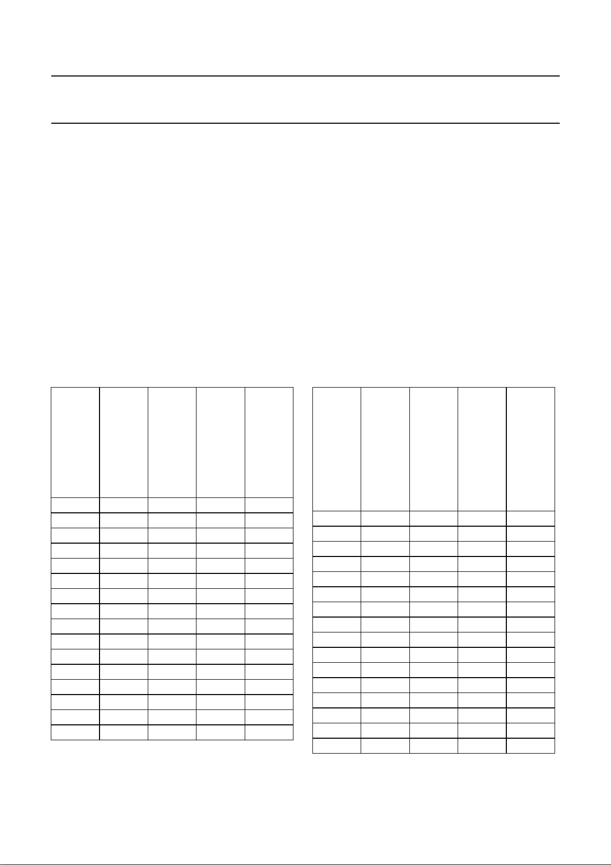
Type Number Definition and Feature Indication
The complete type number of these versions is given below.
UOC
III
series
TDA12000H1/N1VXY0AA
The explanation of the various parts of the type number is given below:
• The first 8 characters indicate the type number, the last 2 characters vary depending on the version.
• The next 1 or 2 characters indicate the envelope. The normal QFP128 version is indicated with “H” and the “face-down
version” with “H1”.
• The first 3 characters after the slash (/) indicate the IC version.
• The characters “X” and “Y” give an indication of the Feature Content. More information is given in the Tables 2 and 3.
• The last 3 characters give an indication of the ROM code.
Table 2 Feature Indication, first character (X) Table 3 Feature Indication, second character (Y)
FIRST INDICATION (X)
00000
10001
20010
30011
40100
50101
60110
70111
81000
91001
A1010
B1011
C1100
D1101
E1110
F1111
ROM size / 0 = 128K
dbx®
Dolby® ProLogic®
Virtual Dolby® (VDS)
TM
SECOND INDICATION (Y)
00000
10001
20010
30011
40100
50101
60110
70111
81000
91001
A1010
B1011
C1100
D1101
E1110
F1111
SRS® 3D Stereo
SRS® TruSurround
BBE
DW / PANORAMA
2003 Dec 18 9
CONFIDENTIAL

Philips Semiconductors Preliminary specification
Versatile signal processor for low- and
mid-range TV applications
UOC
III
series
QUICK REFERENCE DATA
SYMBOL PARAMETER MIN. TYP. MAX. UNIT
Supply
V
P
I
P
V
DDA
I
DDA
V
DDC/P
I
DDC/P
V
PAudio
I
PAudio
P
tot
(1)
(1)
analogue supply voltage TV processor 4.7 5.0 5.3 V
supply current (5.0 V) − 190 − mA
digital supply TV processor / analogue supply periphery 3.0 3.3 3.6 V
supply current (3.3 V) − 36 − mA
digital supply to core/periphery 1.65 1.8 1.95 V
supply current (1.8 V) − 440 − mA
audio supply voltage 4.7 8.0 8.4 V
supply current (5.0/8.0 V) − 0.5 − mA
total power dissipation − 1.87 − W
Input voltages
V
iVIFrms)
V
iSIF(rms)
V
iSSIF(rms)
V
iAUDIO(rms)
V
iCVBS(p-p)
V
iCHROMA(p-p)
video IF amplifier sensitivity (RMS value) − 75 150 µV
QSS sound IF amplifier sensitivity (RMS value) − 45 tbf dBµV
sound IF amplifier sensitivity (RMS value) − 1.0 − mV
external audio input (RMS value) − 1.0 1.3 V
external CVBS/Y input (peak-to-peak value) − 1.0 1.4 V
external chroma input voltage (burst amplitude)
− 0.3 1.0 V
(peak-to-peak value)
V
iRGB(p-p)
V
iY(p-p)
V
iU(p-p)
V
iPB(p-p)
V
iV(p-p) /
V
iPR(p-p)
/
RGB inputs (peak-to-peak value) − 0.7 0.8 V
luminance input signal (peak-to-peak value) − 1.4 / 1.0 − V
U / PB input signal (peak-to-peak value); note 2 −−1.33 /
− V
+0.7
V / PR input signal (peak-to-peak value); note 2 −−1.05 /
− V
+0.7
Output signals
V
o(IFVO)(p-p)
V
o(QSSO)(rms)
V
o(AMOUT)(rms)
V
o(AUDIO)(rms)
V
o(CVBSO)(p-p)
I
o(AGCOUT)
V
oRGB(p-p)
I
oHOUT
I
oVERT
I
oEWD
demodulated CVBS output (peak-to-peak value) − 2.0 − V
sound IF intercarrier output (RMS value) − 100 − mV
demodulated AM sound output (RMS value) − 250 − mV
(1)
non-controlled audio output signals (RMS value) 1.0 −−V
selected CVBS output (peak-to-peak value) − 2.0 − V
tuner AGC output current range 0 − 1mA
RGB output signal amplitudes (peak-to-peak value) − 1.2 − V
horizontal output current 10 −−mA
vertical output current (peak-to-peak value) − 1 − mA
EW drive output current −− 1.2 mA
Note
1. The supply voltage for the analogue audio part of the IC can be 5V or 8V. For a supply voltage of 5V the maximum
signal amplitudes at in and outputs are 1V
2V
.
rms
. For a supply voltage of 8V the maximum output signal amplitude is
rms
2. The YUV/YPBPR input signal amplitudes are based on a colour bar signal with 75/100% saturation.
2003 Dec 18 10
CONFIDENTIAL
Philips Semiconductors Preliminary specification
Versatile signal processor for low- and
mid-range TV applications
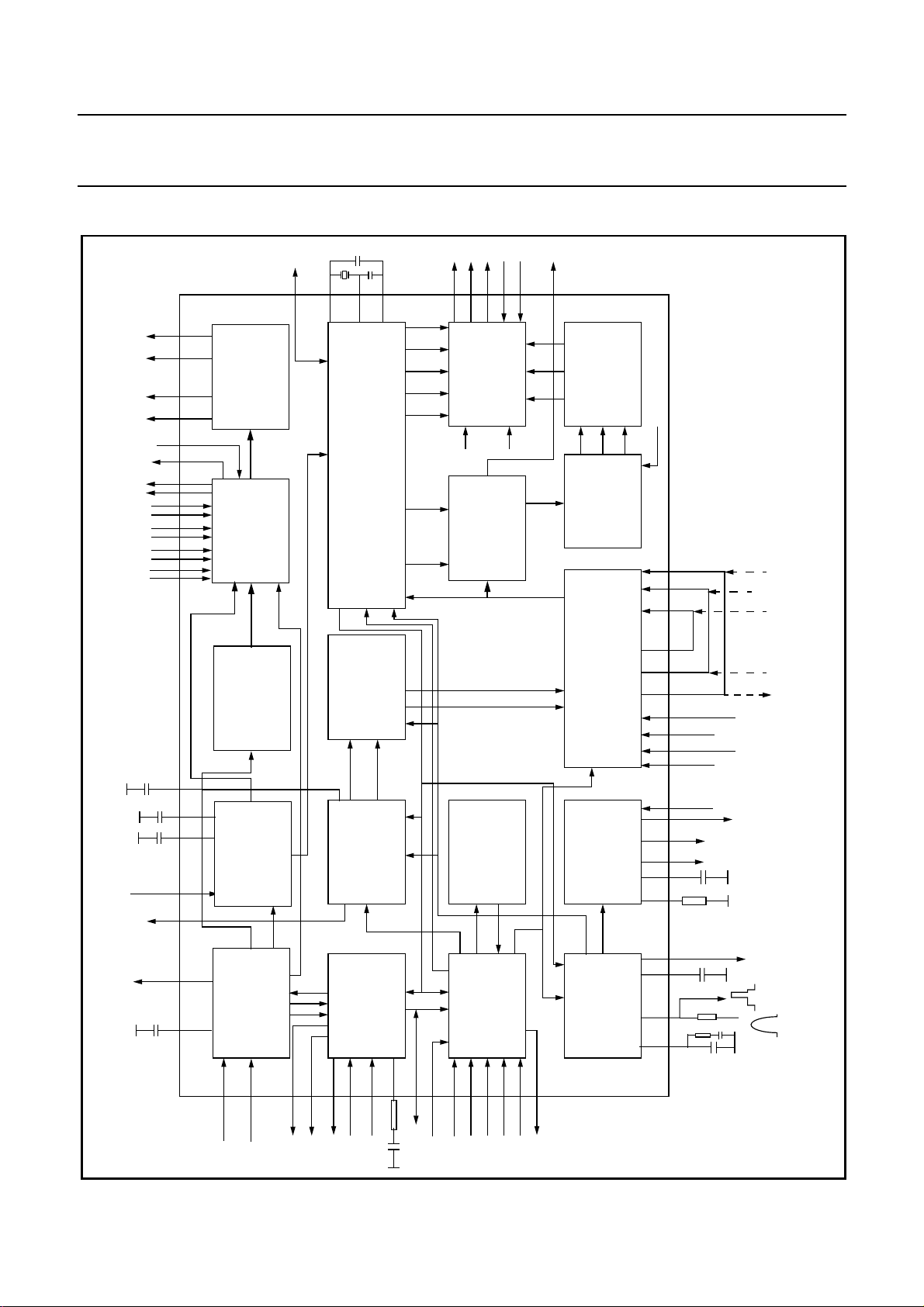
BLOCK DIAGRAMS
I/Os
LR
HP-OUT
R
L
LS-OUT
I2S
SCART/CINCH IN/OUT
AUDIO CONTROL
AUDIO SELECT
A/D CONVERTER
DACs
VOLUME
FEATURES
TREBBLE/BASS
ADC/DAC
AM
STEREO
DECODER
ALL-STANDARD
RDS
DIGITAL SIGNAL PROCESSING FEATURES
µ-PROCESSOR AND TELETEXT DECODER
YUV IN/OUT
BASE-BAND
DELAY LINE
REF
ROGOBO
BL R G B CR
SCAVEM
ON TEXT
BCLIN
CCC
RGB CONTROL
CON.
PEAKING
WHITE-P. ADJ.
CONTR/BRIGHTN
OSD/TEXT INSERT
BRI
U/V DELAY
MODULATION
SCAN VELOCITY
BLKIN
YUV
SVM
RGB MATRIX
BLUE STRETCH
U/V TINT
SKIN TONE
INSERT
B
P
R
RGB/YP
GAMMA CONTROL
BLACK STRETCH
SAT
SATURATION
YUV INTERFACE
Vo Uo Yo Yi Ui Vi
UOC
G/Y
BL
EHTO
III
series
R/P
B
B/P
G/Y
B
SWO1 BL
B/P
R
R/P
EWD
R
(Cx)
(CVBSx/Yx)
DECODER
PAL/SECAM/NTSC
PLL DEMOD.
VIDEO AMP.
SOUND TRAP
GROUP DELAY
VISION IF/AGC/AFC
VIFIN
IFVO/SVO/
CVBSI
C
CVBS2/Y2
YSYNC
SSIF
REFO
QSSO/AMOUT
SOUND PLL
DEEMPHASIS
AGC
SWITCH
QSS MIXER
QSS SOUND IF
SIFIN/DVBIN
AM DEMODULATOR
AGCOUT
DVBO/FMRO
DVBO/IFVO/
FMRO
2003 Dec 18 11
CONFIDENTIAL
2H/4H
DIGITAL
COMB FILTER
Y DELAY ADJ.
VIDEO IDENT.
VIDEO SWITCH
VIDEO FILTERS
CVBS3/Y3
C2/C3
CVBS4/Y4C4CVBSO/
VERTICAL
GEOMETRY
& EAST-WEST
Y
H/V
H/V SYNC SEP.
PIP
LOOP
nd
H-SHIFT
2
H-DRIVE
H-OSC. + PLL
V-DRIVE
HOUT
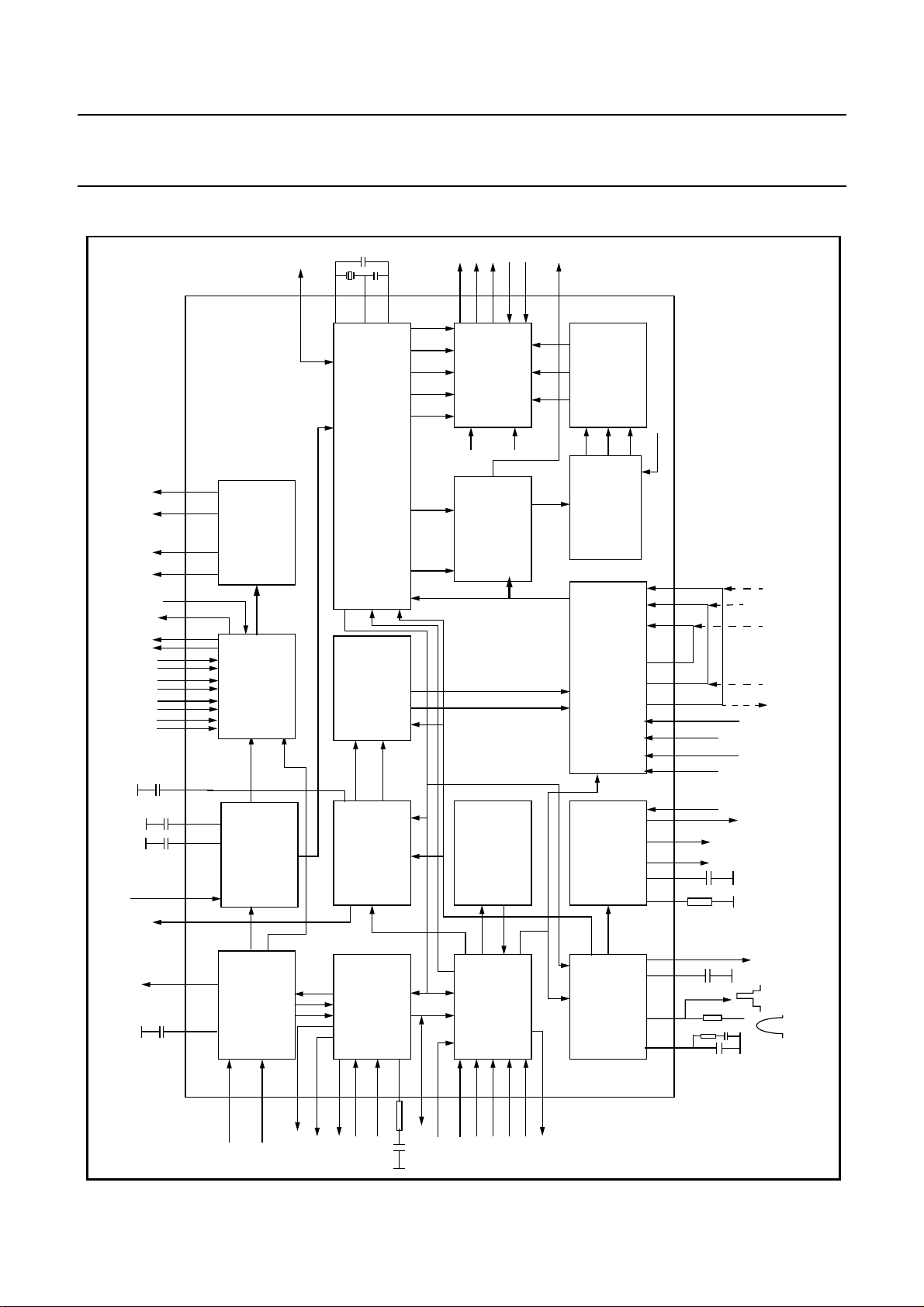
Fig.1 Block diagram of the “Stereo” TV processor
Philips Semiconductors Preliminary specification
Versatile signal processor for low- and
mid-range TV applications
I/Os
BL R G B CR
SCAVEM
ON TEXT
YUV IN/OUT
REF
LR
HP-OUT
R
L
LS-OUT
I2S
SCART/CINCH IN/OUT
AUDIO CONTROL
AUDIO SELECT
DACs
VOLUME
FEATURES
TREBBLE/BASS
ADC/DAC
AM
RDS
DIGITAL SIGNAL PROCESSING FEATURES
µ-PROCESSOR AND TELETEXT DECODER
BASE-BAND
DELAY LINE
ROGOBO
RGB CONTROL
CON.
PEAKING
BCLIN
CCC
WHITE-P. ADJ.
CONTR/BRIGHTN
OSD/TEXT INSERT
BRI
U/V DELAY
MODULATION
SCAN VELOCITY
BLKIN
SVM
RGB MATRIX
BLUE STRETCH
U/V TINT
SKIN TONE
INSERT
B
P
R
YUV INTERFACE
RGB/YP
GAMMA CONTROL
BLACK STRETCH
SAT
SATURATION
UOC
Vi Ui
Yi
Yo
Vo Uo
G/Y
BL
EHTO
III
series
R
R/P
B
B/P
G/Y
BL
B
SWO1
B/P
R
R/P
EWD
(CVBSx/Yx) (Cx)
DECODER
PAL/SECAM/NTSC
PLL DEMOD.
VIDEO AMP.
SOUND TRAP
GROUP DELAY
VISION IF/AGC/AFC
VIFIN
IFVO/SVO/
CVBSI
YSYNC
SSIF
REFO
QSSO/AMOUT
SOUND PLL
DEEMPHASIS
AGC
SWITCH
QSS MIXER
QSS SOUND IF
SIFIN/DVBIN
AM DEMODULATOR
FMRO
AGCOUT
DVBO/FMRO
DVBO/IFVO/
2003 Dec 18 12
CONFIDENTIAL
DIGITAL
2H/4H
COMB FILTER
C
VIDEO IDENT.
VIDEO SWITCH
CVBS3/Y3
C2/C3
CVBS2/Y2
Y DELAY ADJ.
Y
VIDEO FILTERS
CVBS4/Y4C4CVBSO/
PIP
VERTICAL
GEOMETRY
& EAST-WEST
H/V
LOOP
nd
H-SHIFT
2
H/V SYNC SEP.
H-DRIVE
H-OSC. + PLL
V-DRIVE
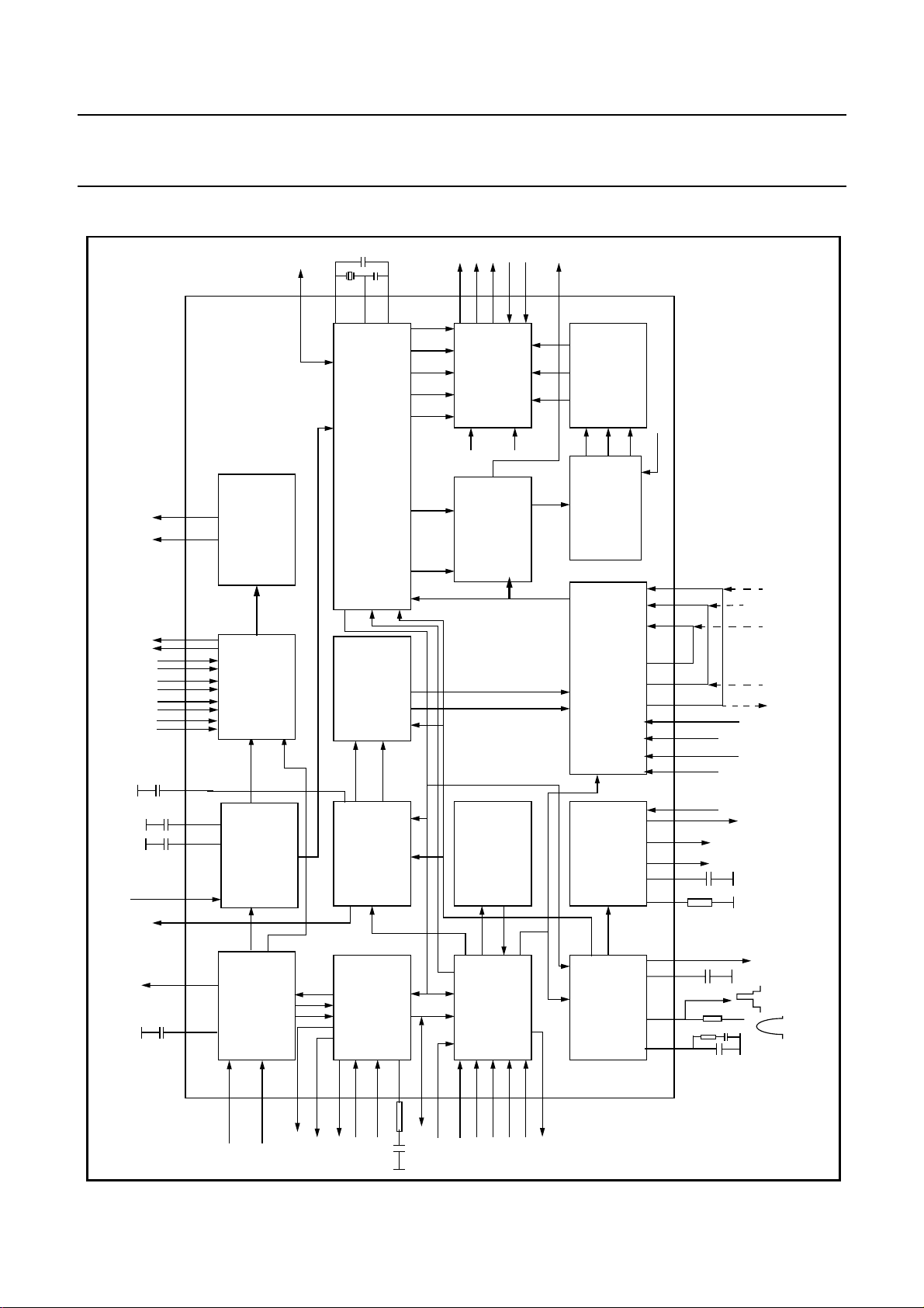
Fig.2 Block diagram of the “AV-stereo” TV processor with audio DSP
HOUT
Philips Semiconductors Preliminary specification
Versatile signal processor for low- and
mid-range TV applications
I/Os
BL R G B CR
SCAVEM
ON TEXT
YUV IN/OUT
REF
R
L
LS-OUT
SCART/CINCH IN/OUT
RDS
VOLUME CONTROL
AUDIO SELECT
AM
DIGITAL SIGNAL PROCESSING FEATURES
µ-PROCESSOR AND TELETEXT DECODER
BASE-BAND
DELAY LINE
ROGOBO
RGB CONTROL
CON.
PEAKING
BCLIN
CCC
WHITE-P. ADJ.
CONTR/BRIGHTN
OSD/TEXT INSERT
BRI
U/V DELAY
MODULATION
SCAN VELOCITY
BLKIN
SVM
RGB MATRIX
BLUE STRETCH
U/V TINT
SKIN TONE
INSERT
B
P
R
YUV INTERFACE
RGB/YP
GAMMA CONTROL
BLACK STRETCH
SAT
SATURATION
UOC
Vi Ui
Yi
Yo
Vo Uo
G/Y
BL
EHTO
III
series
R
R/P
B
B/P
G/Y
BL
B
SWO1
B/P
R
R/P
EWD
(CVBSx/Yx) (Cx)
DECODER
PAL/SECAM/NTSC
PLL DEMOD.
VIDEO AMP.
SOUND TRAP
GROUP DELAY
VISION IF/AGC/AFC
VIFIN
IFVO/SVO/
CVBSI
YSYNC
SSIF
REFO
QSSO/AMOUT
SOUND PLL
DEEMPHASIS
AGC
SWITCH
QSS MIXER
QSS SOUND IF
SIFIN/DVBIN
AM DEMODULATOR
FMRO
AGCOUT
DVBO/FMRO
DVBO/IFVO/
2003 Dec 18 13
CONFIDENTIAL
DIGITAL
2H/4H
C
VIDEO IDENT.
VIDEO SWITCH
CVBS3/Y3
C2/C3
CVBS2/Y2
Y DELAY ADJ.
COMB FILTER
Y
VIDEO FILTERS
CVBS4/Y4C4CVBSO/
PIP
VERTICAL
GEOMETRY
& EAST-WEST
H/V
LOOP
nd
H-SHIFT
2
H/V SYNC SEP.
H-DRIVE
H-OSC. + PLL
V-DRIVE
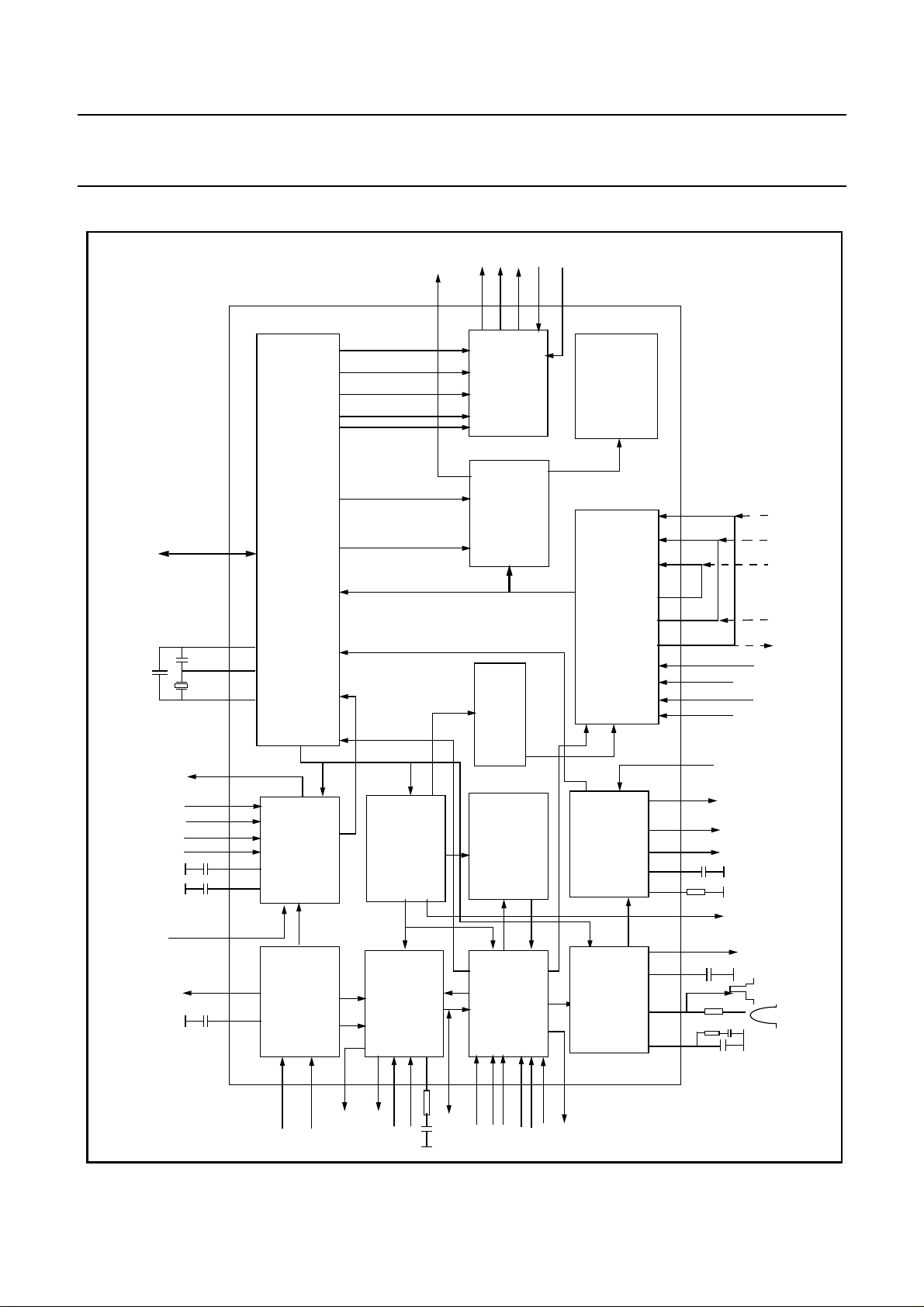
Fig.3 Block diagram of the “AV-stereo” TV processor without audio DSP
HOUT
Philips Semiconductors Preliminary specification
Versatile signal processor for low- and
mid-range TV applications
SVM
SCAVEM
ON TEXT
I/Os
YUV IN/OUT
µ-PROCESSOR AND TELETEXT DECODER
DIGITAL SIGNAL PROCESSING FEATURES
RDS
ROGOBO
RG B BL
BLUE STRETCH
CONTR/BRIGHTN
OSD/TEXT INSERT
COR
PEAKING
SCAN VELOCITY
DELAY LINE
BASE-BAND
BLKIN
BCLIN
CCC
WHITE-P. ADJ.
YUV
U/V DELAY
MODULATION
Y
U/V TINT
SKIN TONE
SATURATION
INSERT
B
P
R
YUV INTERFACE
RGB/YUV/YP
U/V
UOC
BLACK STRETCH
GAMMA CONTROL
I
V
I
U
I
Y
O
Y
O
U
O
V
III
series
B
B/P
R
G/Y
R/P
BL
R
R/P
B
B/P
SWO1 BL G/Y
(CVBS/Yx) (Cx)
AUDOUT/AMOUT
AUDIO5
AUDIO4
AUDIO3
AUDIO2
(AVL)
(SSIF)
QSSO/AMOUT
AUDEEM
SOUND PLL
DEEMPHASIS
AUDIO SWITCH
AGC
SWITCH
QSS MIXER
QSS SOUND IF
SIFIN/DVBIN
AVL
VOLUME CONTROL
AM DEMODULATOR
DVBO/IFVO
FMRO
REF
DECODER
PAL/SECAM/NTSC
REF
PLL DEMOD.
DVB MIXER
SOUND TRAP
GROUP DELAY
VISION IF/AGC/AFC
VIFIN
AGCOUT
IFVO/SVO/
2003 Dec 18 14
CVBS2/Y2
CVBSI
DIGITAL
4H/2H
COMB FILTER
Y DELAY ADJ.
VIDEO IDENT.
VIDEO SWITCH
VIDEO FILTERS
C4
CVBS3/Y3
CVBS4/Y4
C2/C3
VERTICAL + EW
H-OSC. + PLL
H/V SYNC SEP.
CVBSO/PIP
YSYNC
GEOMETRY
AND DRIVE
V
LOOP
nd
H-SHIFT
2
H-DRIVE
EHTO
(EWD)
V-DRIVE
(REFO)
HOUT
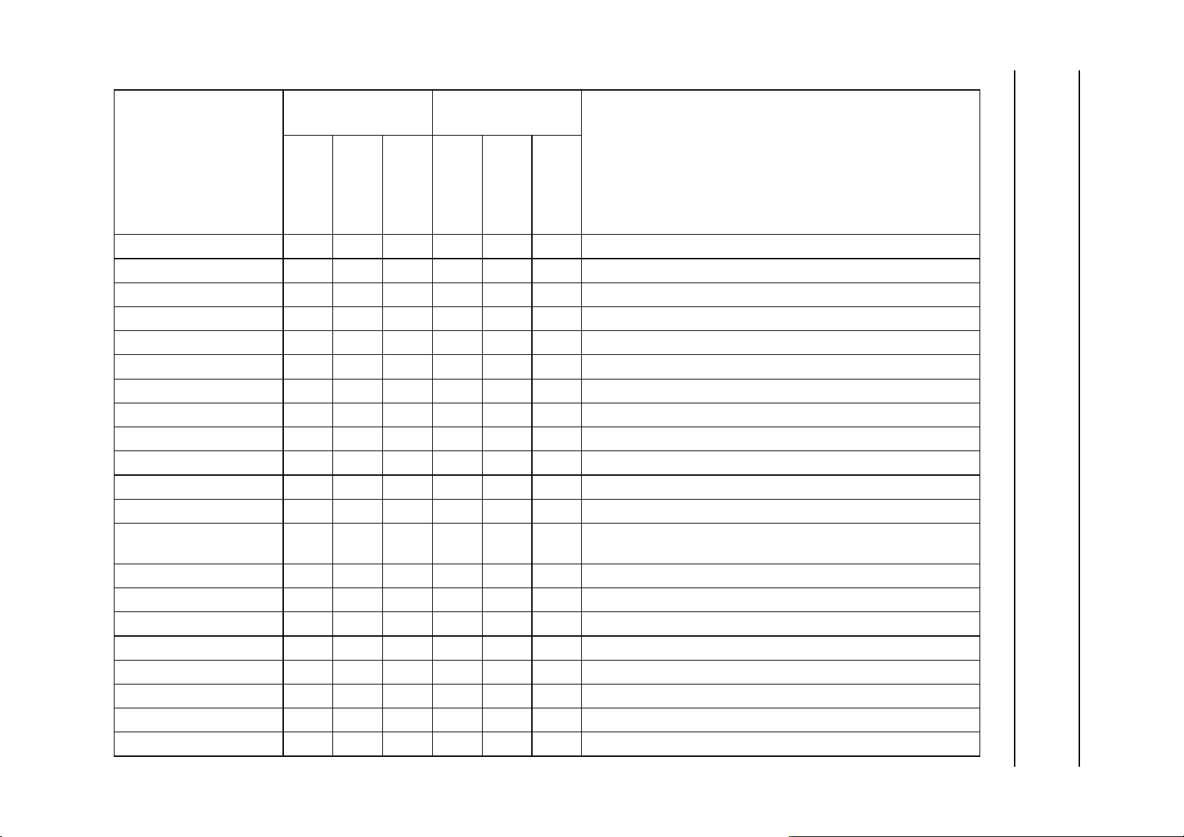
Fig. 4 Block diagram of the “Mono” TV processor
CONFIDENTIAL
2003 Dec 18 15
PINNING OF THE VARIOUS VERSIONS
“STANDARD”
VERSION
AV STEREO
SYMBOL
VSSP2 1 1 1 128 128 128 ground
VSSC4 2 2 2 127 127 127 ground
NO AUDIO DSP
STEREO +
AV STEREO
MONO
“FACE DOWN”
VERSION
AV STEREO
NO AUDIO DSP
STEREO +
AV STEREO
MONO
DESCRIPTION
Philips Semiconductors Preliminary specification
Versatile signal processor for low- and
mid-range TV applications
CONFIDENTIAL
VDDC4 3 3 3 126 126 126 digital supply to SDACs (1.8V)
VDDA3(3.3V) 4 4 4 125 125 125 supply (3.3 V)
VREF_POS_LSL 5 −−124 −−positive reference voltage SDAC (3.3 V)
VREF_NEG_LSL+HPL 6 −−123 −−negative reference voltage SDAC (0 V)
VREF_POS_LSR+HPR 7 −−122 −−positive reference voltage SDAC (3.3 V)
VREF_NEG_HPL+HPR 8 −−121 −−negative reference voltage SDAC (0 V)
VREF_POS_HPR 9 −−120 −−positive reference voltage SDAC (3.3 V)
XTALIN 10 10 10 119 119 119 crystal oscillator input
XTALOUT 11 11 11 118 118 118 crystal oscillator output
VSSA1 12 12 12 117 117 117 ground
VGUARD/SWIO 13 13 13 116 116 116 V-guard input / I/O switch (e.g. 4 mA current sinking capability for
DECDIG 14 14 14 115 115 115 decoupling digital supply
VP1 15 15 15 114 114 114 1
PH2LF 16 16 16 113 113 113 phase-2 filter
PH1LF 17 17 17 112 112 112 phase-1 filter
GND1 18 18 18 111 111 111 ground 1 for TV-processor
SECPLL 19 19 19 110 110 110 SECAM PLL decoupling
direct drive of LEDs)
st
supply voltage TV-processor (+5 V)
UOC
III
series
DECBG 20 20 20 109 109 109 bandgap decoupling
EWD/AVL
(1)
21 21 21 108 108 108 East-West drive output or AVL capacitor
2003 Dec 18 16
“STANDARD”
VERSION
AV STEREO
SYMBOL
VDRB 22 22 22 107 107 107 vertical drive B output
VDRA 23 23 23 106 106 106 vertical drive A output
VIFIN1 24 24 24 105 105 105 IF input 1
NO AUDIO DSP
STEREO +
AV STEREO
MONO
“FACE DOWN”
VERSION
AV STEREO
NO AUDIO DSP
STEREO +
AV STEREO
MONO
DESCRIPTION
Philips Semiconductors Preliminary specification
Versatile signal processor for low- and
mid-range TV applications
CONFIDENTIAL
VIFIN2 25 25 25 104 104 104 IF input 2
VSC 26 26 26 103 103 103 vertical sawtooth capacitor
IREF 27 27 27 102 102 102 reference current input
GNDIF 28 28 28 101 101 101 ground connection for IF amplifier
SIFIN1/DVBIN1
SIFIN2/DVBIN2
AGCOUT 31 31 31 98 98 98 tuner AGC output
EHTO 32 32 32 97 97 97 EHT/overvoltage protection input
AVL/SWO/SSIF/
REFO/REFIN
AUDIOIN5 −−34 −−95 audio 5 input
AUDIOIN5L 34 34 − 95 95 − audio-5 input (left signal)
AUDIOIN5R 35 35 − 94 94 − audio-5 input (right signal)
AUDOUTSL 36 36 − 93 93 − audio output for SCART/CINCH (left signal)
AUDOUTSR 37 37 − 92 92 − audio output for SCART/CINCH (right signal)
DECSDEM 38 38 38 91 91 91 decoupling sound demodulator
QSSO/AMOUT/AUDEEM
(2)
(2)
(2)(3)
29 29 29 100 100 100 SIF input 1 / DVB input 1
30 30 30 99 99 99 SIF input 2 / DVB input 2
33 33 33 96 96 96 Automatic Volume Levelling / switch output / sound IF input /
subcarrier reference output / external reference signal input for I
signal mixer for DVB operation
(2)
39 39 39 90 90 90 QSS intercarrier output / AM output / deemphasis (front-end audio
out)
UOC
III
series
GND2 40 40 40 89 89 89 ground 2 for TV processor

2003 Dec 18 17
SYMBOL
PLLIF 41 41 41 88 88 88 IF-PLL loop filter
SIFAGC/DVBAGC
DVBO/IFVO/FMRO
CONFIDENTIAL
DVBO/FMRO
VCC8V 45 45 45 84 84 84 8 Volt supply for audio switches
AGC2SIF 46 −−83 −−AGC capacitor second sound IF
VP2 47 47 47 82 82 82 2
IFVO/SVO/CVBSI
AUDIOIN4 −−49 −−80 audio 4 input
AUDIOIN4L 49 49 − 80 80 − audio-4 input (left signal)
AUDIOIN4R 50 50 − 79 79 − audio-4 input (right signal)
(2)
(2)
(2)
(2)
“STANDARD”
VERSION
AV STEREO
42 42 42 87 87 87 AGC sound IF / internal-external AGC for DVB applications
43 43 43 86 86 86 Digital Video Broadcast output / IF video output / FM radio output
44 44 − 85 85 − Digital Video Broadcast output / FM radio output
48 48 48 81 81 81 IF video output / selected CVBS output / CVBS input
NO AUDIO DSP
STEREO +
AV STEREO
MONO
“FACE DOWN”
VERSION
AV STEREO
NO AUDIO DSP
STEREO +
AV STEREO
MONO
DESCRIPTION
nd
supply voltage TV processor (+5 V)
Philips Semiconductors Preliminary specification
Versatile signal processor for low- and
mid-range TV applications
CVBS4/Y4 51 51 51 78 78 78 CVBS4/Y4 input
C4 52 52 52 77 77 77 chroma-4 input
AUDIOIN2 −−53 −−76 audio 2 input
AUDIOIN2L/SSIF
AUDIOIN2R 54 54 − 75 75 − audio 2 input (right signal)
CVBS2/Y2 55 55 55 74 74 74 CVBS2/Y2 input
AUDIOIN3 −−56 −−73 audio 3 input
AUDIOIN3L 56 56 − 73 73 − audio 3 input (left signal)
AUDIOIN3R 57 57 − 72 72 − audio 3 input (right signal)
CVBS3/Y3 58 58 58 71 71 71 CVBS3/Y3 input
C2/C3 59 59 59 70 70 70 chroma-2/3 input
(3)
53 53 − 76 76 − audio 2 input (left signal) / sound IF input
UOC
III
series

2003 Dec 18 18
“STANDARD”
VERSION
AV STEREO
SYMBOL
AUDOUTLSL 60 62 − 69 67 − audio output for audio power amplifier (left signal)
AUDOUTLSR 61 63 − 68 66 − audio output for audio power amplifier (right signal)
AUDOUT/AMOUT/FMOUT −−62 −−67 audio output / AM output / FM output, volume controlled
NO AUDIO DSP
STEREO +
AV STEREO
MONO
“FACE DOWN”
VERSION
AV STEREO
NO AUDIO DSP
STEREO +
AV STEREO
MONO
DESCRIPTION
Philips Semiconductors Preliminary specification
Versatile signal processor for low- and
mid-range TV applications
CONFIDENTIAL
AUDOUTHPL 62 −−67 −−audio output for headphone channel (left signal)
AUDOUTHPR 63 −−66 −−audio output for headphone channel (right signal)
CVBSO/PIP 64 64 64 65 65 65 CVBS / PIP output
SVM 65 65 65 64 64 64 scan velocity modulation output
FBISO/CSY 66 66 66 63 63 63 flyback input/sandcastle output or composite H/V timing output
HOUT 67 67 67 62 62 62 horizontal output
VSScomb 68 68 68 61 61 61 ground connection for comb filter
VDDcomb 69 69 69 60 60 60 supply voltage for comb filter (5 V)
VIN (R/P
UIN (B/PBIN2) 71 71 71 58 58 58 U-input for YUV interface (2
YIN (G/YIN2/CVBS-Y
YSYNC 73 73 73 56 56 56 Y-input for sync separator
YOUT 74 74 74 55 55 55 Y-output (for YUV interface)
UOUT (INSSW2) 75 75 75 54 54 54 U-output for YUV interface (2
VOUT (SWO1) 76 76 76 53 53 53 V-output for YUV interface (general purpose switch output)
INSSW3 77 77 77 52 52 52 3
R/P
G/YIN3 79 79 79 50 50 50 3
IN2/CX) 70 70 70 59 59 59 V-input for YUV interface (2nd R input / PR input or CX input)
R
IN3 78 78 78 51 51 51 3rd R input / PR input
R
nd
B input / PB input)
) 72 72 72 57 57 57 Y-input for YUV interface (2nd G input / Y input or CVBS/YX input))
X
nd
RGB / YPBPRinsertion input)
rd
RGB / YPBPRinsertion input
rd
G input / Y input
UOC
III
series
B/P
IN3 80 80 80 49 49 49 3rd B input / PB input
B
2003 Dec 18 19
“STANDARD”
VERSION
AV STEREO
SYMBOL
GND3 81 81 81 48 48 48 ground 3 for TV-processor
VP3 82 82 82 47 47 47 3
BCLIN 83 83 83 46 46 46 beam current limiter input
NO AUDIO DSP
STEREO +
AV STEREO
MONO
“FACE DOWN”
VERSION
AV STEREO
NO AUDIO DSP
STEREO +
AV STEREO
MONO
rd
supply for TV processor
DESCRIPTION
Philips Semiconductors Preliminary specification
Versatile signal processor for low- and
mid-range TV applications
CONFIDENTIAL
BLKIN 84 84 84 45 45 45 black current input
RO 85 85 85 44 44 44 Red output
GO 86 86 86 43 43 43 Green output
BO 87 87 87 42 42 42 Blue output
VDDA1 88 88 88 41 41 41 analog supply for TCG µ-Controller and digital supply for
VREFAD_NEG 89 89 89 40 40 40 negative reference voltage (0 V)
VREFAD_POS 90 90 90 39 39 39 positive reference voltage (3.3 V)
VREFAD 91 −−38 −−reference voltage for audio ADCs (3.3/2 V)
GNDA 92 92 92 37 37 37 ground
VDDA(1.8V) 93 93 93 36 36 36 analogue supply for audio ADCs (1.8 V)
VDDA2(3.3) 94 94 94 35 35 35 supply voltage SDAC (3.3 V)
VSSadc 95 95 95 34 34 34 ground for video ADC and PLL
VDDadc(1.8) 96 96 96 33 33 33 supply voltage video ADC and PLL
INT0/P0.5 97 97 97 32 32 32 external interrupt 0 or port 0.5 (4 mA current sinking capability for
P1.0/INT1 98 98 98 31 31 31 port 1.0 or external interrupt 1
P1.1/T0 99 99 99 30 30 30 port 1.1 or Counter/Timer 0 input
TV-processor (+3.3 V)
direct drive of LEDs)
UOC
III
series
VDDC2 100 100 100 29 29 29 digital supply to core (1.8 V)
VSSC2 101 101 101 28 28 28 ground
2003 Dec 18 20
“STANDARD”
VERSION
AV STEREO
SYMBOL
P0.4/I2SWS 102 −−27 −−port 0.4 or I2S word select
P0.4 − 102 102 − 27 27 port 0.4
P0.3/I2SCLK 103 −−26 −−port 0.3 or I2S clock
NO AUDIO DSP
STEREO +
AV STEREO
MONO
“FACE DOWN”
VERSION
AV STEREO
NO AUDIO DSP
STEREO +
AV STEREO
MONO
DESCRIPTION
Philips Semiconductors Preliminary specification
Versatile signal processor for low- and
mid-range TV applications
CONFIDENTIAL
P0.3 − 103 103 − 26 26 port 0.3
P0.2/I2SDO2 104 −−25 −−port 0.2 or I
P0.2 − 104 104 − 25 25 port 0.2
P0.1/I2SDO1 105 −−24 −−port 0.1 or I2S digital output 1
P0.1 − 105 105 − 24 24 port 0.1
P0.0/I2SDI1/O 106 −−23 −−port 0.0 or I2S digital input 1 or I2S digital output
P0.0 − 106 106 − 23 23 port 0.0
P1.3/T1 107 107 107 22 22 22 port 1.3 or Counter/Timer 1 input
P1.6/SCL 108 108 108 21 21 21 port 1.6 or I
P1.7/SDA 109 109 109 20 20 20 port 1.7 or I
VDDP(3.3V) 110 110 110 19 19 19 supply to periphery and on-chip voltage regulator (3.3 V)
P2.0/TPWM 111 111 111 18 18 18 port 2.0 or Tuning PWM output
P2.1/PWM0 112 112 112 17 17 17 port 2.1 or PWM0 output
P2.2/PWM1 113 113 113 16 16 16 port 2.2 or PWM1 output
P2.3/PWM2 114 114 114 15 15 15 port 2.3 or PWM2 output
P3.0/ADC0 115 115 115 14 14 14 port 3.0 or ADC0 input
P3.1/ADC1 116 116 116 13 13 13 port 3.1 or ADC1 input
VDDC1 117 117 117 12 12 12 digital supply to core (+1.8 V)
2
S digital output 2
2
C-bus clock line
2
C-bus data line
UOC
III
series
DECV1V8 118 118 118 11 11 11 decoupling 1.8 V supply
2003 Dec 18 21
“STANDARD”
VERSION
AV STEREO
SYMBOL
P3.2/ADC2 119 119 119 10 10 10 port 3.2 or ADC2 input
P3.3/ADC3 120 120 120 9 9 9 port 3.3 or ADC3 input
VSSC/P 121 121 121 8 8 8 digital ground for µ-Controller core and periphery
NO AUDIO DSP
STEREO +
AV STEREO
MONO
“FACE DOWN”
VERSION
AV STEREO
NO AUDIO DSP
STEREO +
AV STEREO
MONO
DESCRIPTION
Philips Semiconductors Preliminary specification
Versatile signal processor for low- and
mid-range TV applications
CONFIDENTIAL
P2.4/PWM3 122 122 122 7 7 7 port 2.4 or PWM3 output
P2.5/PWM4 123 123 123 6 6 6 port 2.5 or PWM4 output
VDDC3 124 124 124 5 5 5 digital supply to core (1.8V)
VSSC3 125 125 125 4 4 4 ground
P1.2/INT2 126 126 126 3 3 3 port 1.2 or external interrupt 2
P1.4/RX 127 127 127 2 2 2 port 1.4 or UART bus
P1.5/TX 128 128 128 1 1 1 port 1.5 or UART bus
Note
1. The function of this pin can be chosen by means of the AVLE bit.
2. The functional content of these pins is dependent on the mode of operation and on some I2C-bus control bits. More details are given in table 4.
3. With the ESSIF bit the SSIF input can be selected either on pin 33 or pin 53. For the “face down” versions these pin numbers are 96 and 76
respectively.
UOC
III
series
2003 Dec 18 22
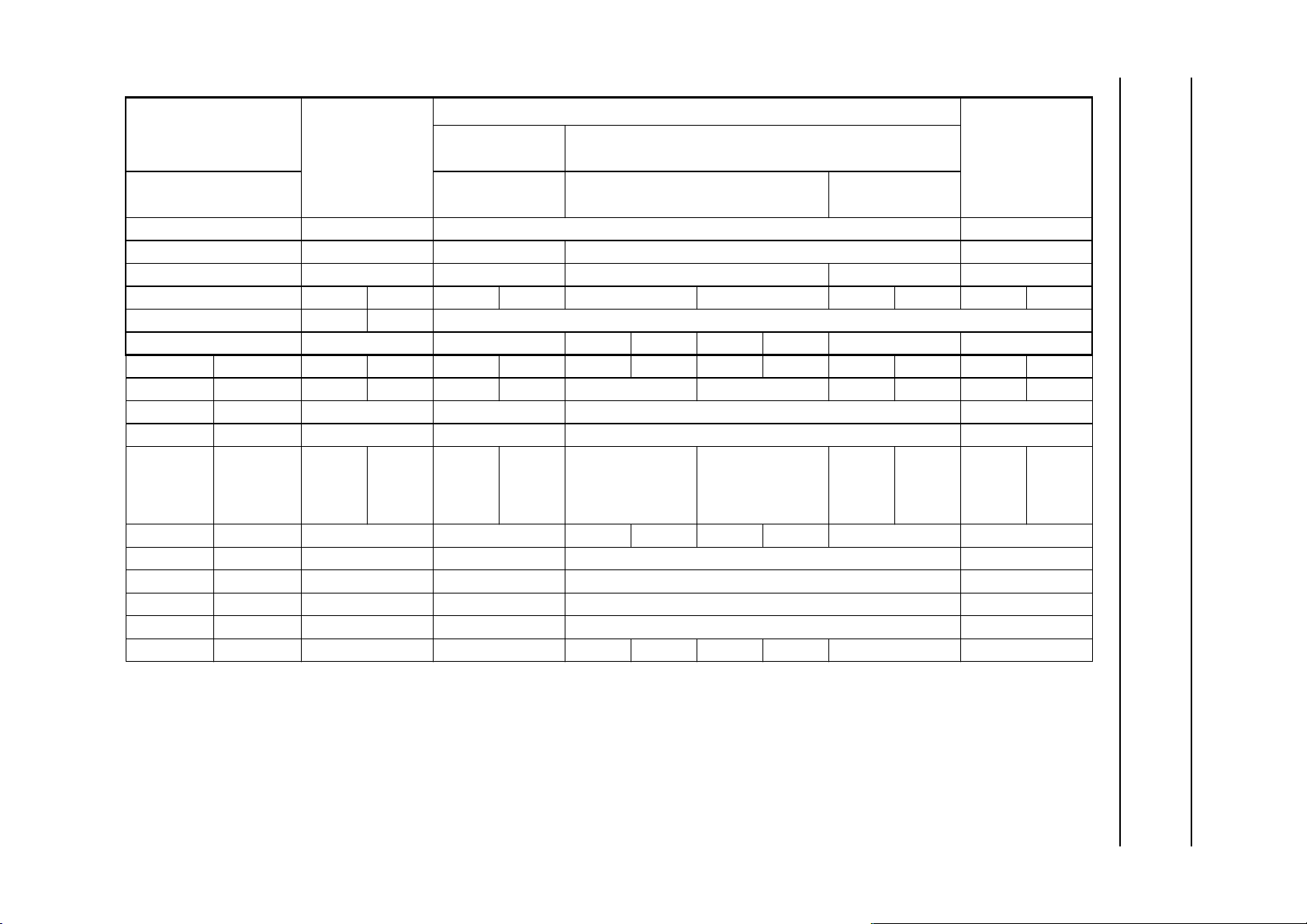
Table 4 Pin functions for various modes of operation
IC MODE
DVB MODE
FM-PLL MODE
(QSS = 0)
ANALOGUE TV MODE
QSS MODE (QSS = 1)
FM RADIO MODE
Philips Semiconductors Preliminary specification
Versatile signal processor for low- and
mid-range TV applications
FUNCTION
IFA/IFB/IFC bits 101/111 000/001/010/011/100/110 101/111
FMR bit 0 0 0 1
FMI bit −− 01−
AVLE bit 1010 1 0 1010
CONFIDENTIAL
CMB2/CMB1/CMB0 bits 010/011 100 000/001/010/011/101/110
AM bit −−0101 −−
Standard Face-down
pin 21 pin 108 AVL EWD AVL EWD AVL EWD AVL EWD AVL EWD
pin 29 pin 100 DVBIN1 − SIFIN1 SIFIN1
pin 30 pin 99 DVBIN2 − SIFIN2 SIFIN2
(1)
pin 33
pin 39 pin 90 − AUDEEM QSSO AMOUT QSSO AMOUT AUDEEM AUDEEM
pin 42 pin 87 DVBAGC − SIFAGC SIFAGC
pin 43
pin 44
pin 48
pin 62
(2)
(2)
(3)
(4)
pin 96
pin 86
pin 85
pin 81
pin 67
(1)
(2)
(2)
(3)
(4)
FM
DEMODULATION
SWO REFIN SWO/
SSIF/
REFO
DVBO IFVO IFVO FMRO
DVBO −−FMRO
SVO/CVBSI IFVO/SVO/CVBSI IFVO/SVO/CVBSI IFVO/SVO/CVBSI
AUDOUT AUDOUT AUDOUT AMOUT AUDOUT AMOUT AUDOUT AUDOUT
AVL/
SWO/
SSIF/
REFO
QSS/AM DEMODULATION
SWO/SSIF/REFO AVL/SWO/SSIF/
REFO
QSS-FM
DEMODULATION
SWO/
SSIF/
REFO
AVL/
SWO/
SSIF/
REFO
SWO/
SSIF/
REFO
AVL/
SWO/
SSIF/
REFO
Note
1. The function of this pin is controlled by the bits CMB2-CMB0 in subaddress 4AH.
2. The functions of the pins 43/44 (standard pinning) or 85/86 (face-down pinning) are controlled by the IFO2-IFO0 bits in subaddress 31H.
3. The function of this pin is determined by the SVO1/SVO0 bits in subaddress 39H.
4. This functionality is only valid for the mono versions. In the “stereo” and “AV-stereo” versions this pin has the function of audio output for the
headphone channel (left signal).
UOC
III
series

Philips Semiconductors Preliminary specification
Versatile signal processor for low- and
mid-range TV applications
P3.2/ADC2
P3.3/ADC3
120
119
42
41
PLLIF
GND2
DECV1V8
VDDC1(1.8)
118
43
SIFAGC/DVBAGC
DVBO//IFVO/FMRO
117
44
DVBO/FMRO
VSSP2
VSSC4
VDDC4
VDDA3(3.3V)
VREF_POS_LSL
VREF_NEG_LSL+LSR
VREF_POS_LSR+HPL
VREF_NEG_HPL+HPR
VREF_POS_HPR
XTALIN
XTALOUT
VSSA1
VGUARD/SWIO
DECDIG
VP1
PH2LF
PH1LF
GND1
SECPLL
DECBG
AVL/EWD
VDRB
VDRA
VIFIN1
VIFIN2
VSC
IREF
GNDIF
DVBIN1/SIFIN1
DVBIN2/SIFIN2
AGCOUT
EHTO
P1.4/RX
P1.2/INT2
P1.5/TX
127
128
1
2
3
4
5
6
7
8
9
10
11
12
13
14
15
16
17
18
19
20
21
22
23
24
25
26
27
28
29
30
31
32
QFP-128 0.8mm pitch “standard version”
34
33
AUDIOIN5L
REFIN/REFOUT
AVL/SWO/SSIF/
VDDC3
VSSC3
125
124
126
37
35
36
AUDOUTSL
AUDIOIN5R
AUDOUTSR
VSSC1/P
P2.4/PWM3
P2.5/PWM4
121
122
123
39
40
38
DECSDEM
P3.1/ADC1
P3.0/ADC0
P2.3/PWM2
114
115
116
47
45
46
VP2
VCC8V
AGC2SIF
P2.2/PWM1
P2.1/PWM0
P2.0/PMW
VDDP(3.3V)
111
112
113
110
50
48
49
51
CVBS4/Y4
AUDIOIN4L
AUDIOIN4R
SVO/IFOUT/CVBSI
P1.6/SCL
P1.7/SDA
109
108
52
C4
53
AUDIOIN2L
P1.3/T1
P0.0/I2SDI1
P0.1/I2SDO1
P0.2/I2SDO2
107
104
105
106
54
AUDIOIN2R/SSIF
575859
56
55
AUDIOIN3L
CVBS2/Y2
AUDIOIN3R
P0.4/I2SWS
VSSC2
103
102
101
C2/C3
CVBS3/Y3
VDDC2
100
60
AUDOUTLSL
P0.3/I2SCLK
UOC
P1.O/INT1
INT0/P0.5
P1.1/T0
99
97
98
61
62
63
AUDOUTHPL
AUDOUTLSR
AUDOUTHPR
III
series
VDDadc(1.8)
96
VSSadc
95
VDDA2(3.3V)
94
93
VDDA(1.8V)
GNDA
92
VREFAD
91
VREFAD_POS
90
VREFAD_NEG
89
VDDA1(3.3V.)
88
BO
87
GO
86
RO
85
BLKIN
84
BCLIN
83
82
VP3
GND3
81
80
79
78
77
76
75
74
73
72
71
70
69
68
67
66
65
64
CVBSO/PIP
-3
B/P
B
G/Y-3
-3
R/P
R
INSSW3
VOUT(SWO1)
UOUT(INSW-2)
YOUT
YSYNC
YIN(G/Y-2/CVBS/Y-X)
(B/PB-2)
UIN
VIN(R/P
R
VDDcomb
VSScomb
HOUT
FBISO/CSY
SVM
-2/C-X)
AMOUT/QSSO/AUDEEM
Fig.5 Pin configuration “stereo” and “AV-stereo” versions with Audio DSP
2003 Dec 18 23
CONFIDENTIAL

Philips Semiconductors Preliminary specification
Versatile signal processor for low- and
mid-range TV applications
DECV1V8
P3.2/ADC2
VDDC1(1.8)
117
119
118
42
43
44
-
SIFAGC/DVBAGC
DVBO//IFVO/FMRO
P3.1/ADC1
P3.0/ADC0
P2.3/PWM2
114
115
116
47
45
46
VP2
VCC8V
VSSP2
VSSC4
VDDC4
VDDA3(3.3V)
XTALIN
XTALOUT
VSSA1
VGUARD/SWIO
DECDIG
VP1
PH2LF
PH1LF
GND1
SECPLL
DECBG
AVL/EWD
VDRB
VDRA
VIFIN1
VIFIN2
VSC
IREF
GNDIF
DVBIN1/SIFIN1
DVBIN2/SIFIN2
AGCOUT
EHTO
VDDC3
VSSC3
P1.4/RX
P1.2/INT2
P1.5/TX
125
127
128
1
2
3
4
-
5
-
6
-
7
-
8
-
9
10
11
12
13
14
15
16
17
18
19
20
21
22
23
24
25
26
27
28
29
30
31
32
QFP-128 0.8mm pitch “standard version”
34
33
AUDIOIN5L
REFIN/REFOUT
AVL/SWO/SSIF/
124
126
37
35
36
AUDOUTSL
AUDIOIN5R
AUDOUTSR
VSSC1/P
P2.4/PWM3
P2.5/PWM4
121
122
123
39
40
38
GND2
DECSDEM
P3.3/ADC3
120
41
PLLIF
P2.2/PWM1
P2.1/PWM0
P2.0/PMW
VDDP(3.3V)
P1.7/SDA
111
112
113
48
SVO/IFOUT/CVBSI
110
50
49
51
CVBS4/Y4
AUDIOIN4L
AUDIOIN4R
P1.6/SCL
P1.3/T1
P0.0
107
109
108
53
54
52
C4
AUDIOIN2R
AUDIOIN2L/SSIF
P0.1
P0.2
104
105
106
575859
56
55
AUDIOIN3L
CVBS2/Y2
AUDIOIN3R
VSSC2
P0.3
P0.4
103
102
101
60
-
C2/C3
CVBS3/Y3
P1.1/T0
VDDC2
99
100
61
62
-
AUDOUTLSL
UOC
P1.O/INT1
INT0/P0.5
97
98
96
95
94
93
92
91
90
89
88
87
86
85
84
83
82
81
80
79
78
77
76
75
74
73
72
71
70
69
68
67
66
65
64
63
CVBSO/PIP
AUDOUTLSR
III
series
VDDadc(1.8)
VSSadc
VDDA2(3.3V)
VDDA(1.8V)
GNDA
-
VREFAD_POS
VREFAD_NEG
VDDA1(3.3V.)
BO
GO
RO
BLKIN
BCLIN
VP3
GND3
-3
B/P
B
G/Y-3
-3
R/P
R
INSSW3
VOUT(SWO1)
UOUT(INSW-2)
YOUT
YSYNC
YIN(G/Y-2/CVBS/Y-X)
(B/PB-2)
UIN
VIN(R/P
VDDcomb
VSScomb
HOUT
FBISO/CSY
SVM
-2/C-X)
R
AMOUT/QSSO/AUDEEM
Fig.6 Pin configuration of “AV stereo” versions without Audio DSP
2003 Dec 18 24
CONFIDENTIAL

Philips Semiconductors Preliminary specification
Versatile signal processor for low- and
mid-range TV applications
P3.1/ADC1
DECV1V8
VDDC1(1.8)
117
116
118
43
44
-
DVBO//IFVO/FMRO
P3.0/ADC0
P2.3/PWM2
114
115
45
46
-
VCC8V
47
VP2
VSSP2
VSSC4
VDDC4
VDDA3(3.3V)
XTALIN
XTALOUT
VSSA1
VGUARD/SWIO
DECDIG
VP1
PH2LF
PH1LF
GND1
SECPLL
DECBG
AVL/EWD
VDRB
VDRA
VIFIN1
VIFIN2
VSC
IREF
GNDIF
DVBIN1/SIFIN1
DVBIN2/SIFIN2
AGCOUT
EHTO
P1.4/RX
P1.5/TX
127
128
1
2
3
4
-
5
-
6
-
7
-
8
-
9
10
11
12
13
14
15
16
17
18
19
20
21
22
23
24
25
26
27
28
29
30
31
32
QFP-128 0.8mm pitch “standard version”
34
33
AUDIOIN5
REFIN/REFOUT
AVL/SWO/SSIF/
VDDC3
VSSC3
P1.2/INT2
125
124
126
37
35
36
-
-
-
VSSC1/P
P2.4/PWM3
P2.5/PWM4
121
122
123
39
40
38
GND2
DECSDEM
P3.2/ADC2
P3.3/ADC3
120
119
42
41
PLLIF
SIFAGC/DVBAGC
P2.2/PWM1
P2.1/PWM0
P2.0/PMW
VDDP(3.3V)
111
112
113
110
50
48
49
51
-
AUDIOIN4
CVBS4/Y4
SVO/IFOUT/CVBSI
P1.6/SCL
P1.7/SDA
109
108
52
C4
AUDIOIN2
P1.3/T1
107
53
-
P0.1
P0.0
106
54
55
CVBS2/Y2
P0.2
104
105
575859
56
-
AUDIOIN3
P0.3
P0.4
VSSC2
103
102
101
60
C2/C3
CVBS3/Y3
P1.O/INT1
P1.1/T0
VDDC2
99
100
61
62
-
-
AUDOUT/AMOUT
UOC
INT0/P0.5
97
98
64
63
-
CVBSO/PIP
III
series
VDDadc(1.8)
96
VSSadc
95
94
VDDA2(3.3V)
93
VDDA(1.8V)
GNDA
92
-
91
VREFAD_POS
90
VREFAD_NEG
89
VDDA1(3.3V.)
88
BO
87
GO
86
RO
85
BLKIN
84
BCLIN
83
82
VP3
GND3
81
80
68
67
66
-3
B/P
B
G/Y-3
79
-3
R/P
R
78
INSSW3
77
VOUT(SWO1)
76
UOUT(INSW-2)
75
YOUT
74
YSYNC
73
YIN(G/Y-2/CVBS/Y-X)
72
(B/PB-2)
UIN
71
VIN(R/P
70
VDDcomb
69
VSScomb
HOUT
FBISO/CSY
SVM
65
-2/C-X)
R
AMOUT/QSSO/AUDEEM
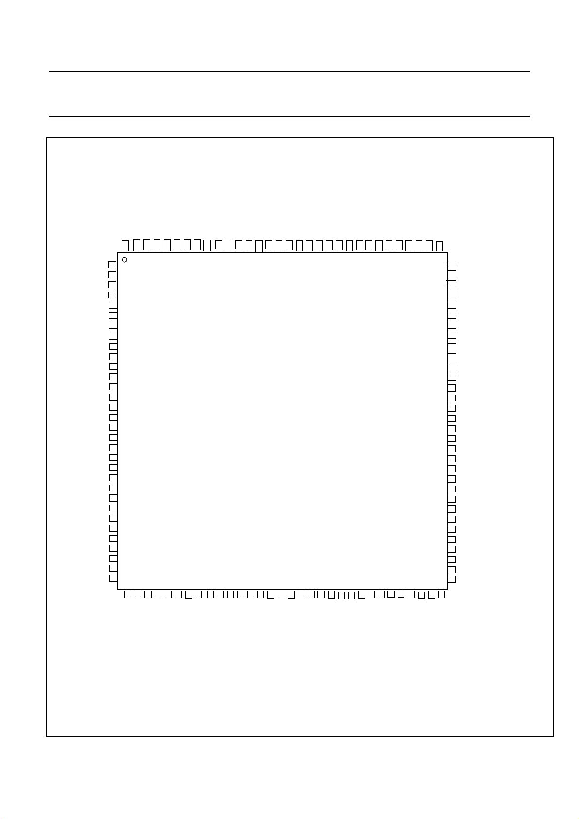
Fig.7 Pin configuration “mono” versions
2003 Dec 18 25
CONFIDENTIAL
Philips Semiconductors Preliminary specification
Versatile signal processor for low- and
mid-range TV applications
P1.5/TX
P1.4/RX
P1.2/INT2
VSSC3
VDDC3
P2.5/PWM4
P2.4/PWM3
VSSC1/P
P3.3/ADC3
P3.2/ADC2
DECV1V8
VDDC1(1.8)
P3.1/ADC1
P3.0/ADC0
P2.3/PWM2
P2.2/PWM1
P2.1/PWM0
P2.0/PMW
VDDP(3.3V)
P1.7/SDA
P1.6/SCL
P1.3/T1
P0.0/I2SDI1
P0.1/I2SDO1
P0.2/I2SDO2
P0.3/I2SCLK
P0.4/I2SWS
VSSC2
VDDC2
P1.1/T0
P1.O/INT1
INT0/P0.5
VDDA3(3.3V)
VSSC4
VSSP2
VDDC4
127
126
128
1
2
3
4
5
6
7
8
9
10
11
12
13
14
15
16
17
18
19
20
21
22
23
24
25
26
27
28
29
30
31
32
QFP-128 0.8 mm pitch “face down version”
34
33
VSSadc
VDDadc(1.8)
VDDA2(3.3V)
VREF_NEG_LSL+LSR
VREF_POS_LSL
125
123
124
37
35
38
36
GNDA
VREFAD
VDDA(1.8V)
VREF_POS_LSR+HPL
122
39
VREFAD_POS
XTALIN
VREF_NEG_HPL+HPR
VREF_POS_HPR
XTALOUT
121
120
119
118
42
40
VREFAD_NEG
41
VDDA1(3.3V.)
43
BOGORO
VSSA1
VGUARD/SWIO
117
116
45
44
BLKIN
DECDIG
VP1
114
115
47
46
VP3
BCLIN
PH2LF
113
PH1LF
112
48
49
-3
B
GND3
B/P
GND1
SECPLL
111
50
G/Y-3
110
51
-3
R
R/P
AVL/EWD
DECBG
109
108
53
52
INSSW3
VOUT(SWO1)
VDRB
VDRA
107
106
54
UOUT(INSW-2)
55
YOUT
VIFIN1
VIFIN2
104
105
575859
56
YSYNC
YIN(G/Y-2/CVBS/Y-X)
VSC
103
-2)
B
(B/P
UIN
IREF
GNDIF
102
101
60
-2/C-X)
R
VDDcomb
VIN(R/P
UOC
DVBIN2/SIFIN2
AGCOUT
99
61
EHTO
97
98
62
63
HOUT
FBISO/CSY
64
SVM
DVBIN1/SIFIN1
100
VSScomb
III
series
AVL/SWO/SSIF/
REFIN/REFOUT
96
95
AUDIOIN5L
94
AUDIOIN5R
AUDOUTSL
93
92
AUDOUTSR
91
DECSDEM
AMOUT/QSSO/AUDEEM
90
89
GND2
PLLIF
88
87
SIFAGC/DVBAGC
DVBO//IFVO/FMRO
86
85
DVBO/FMRO
84
VCC8V
83
AGC2SIF
82
VP2
SVO/IFOUT/CVBSI
81
80
AUDIOIN4L
AUDIOIN4R
79
78
CVBS4/Y4
77
C4
76
AUDIOIN2L/SSIF
AUDIOIN2R
75
74
CVBS2/Y2
AUDIOIN3L
73
72
AUDIOIN3R
CVBS3/Y3
71
70
C2/C3
69
AUDOUTLSL
68
AUDOUTLSR
67
AUDOUTHPL
66
AUDOUTHPR
65
CVBSO/PIP
Fig.8 Pin configuration “stereo” and “AV-stereo” versions with Audio DSP
2003 Dec 18 26
CONFIDENTIAL

Philips Semiconductors Preliminary specification
Versatile signal processor for low- and
mid-range TV applications
VDDA3(3.3V)
P1.5/TX
P1.4/RX
P1.2/INT2
VSSC3
VDDC3
P2.5/PWM4
P2.4/PWM3
VSSC1/P
P3.3/ADC3
P3.2/ADC2
DECV1V8
VDDC1(1.8)
P3.1/ADC1
P3.0/ADC0
P2.3/PWM2
P2.2/PWM1
P2.1/PWM0
P2.0/PMW
VDDP(3.3V)
P1.7/SDA
P1.6/SCL
P1.3/T1
P0.0
P0.1
P0.2
P0.3
P0.4
VSSC2
VDDC2
P1.1/T0
P1.O/INT1
INT0/P0.5
VSSC4
VSSP2
VDDC4
-
---
-
124
37
36
GNDA
VDDA(1.8V)
123
38
-
122
39
125
127
126
128
1
2
3
4
5
6
7
8
9
10
11
12
13
14
15
16
17
18
19
20
21
22
23
24
25
26
27
28
29
30
31
32
QFP-128 0.8mm pitch “face down version”
34
35
33
VSSadc
VDDadc(1.8)
VDDA2(3.3V)
121
120
40
VREFAD_NEG
VREFAD_POS
XTALIN
119
42
41
BOGORO
VDDA1(3.3V.)
XTALOUT
118
43
VSSA1
VGUARD/SWIO
117
116
45
44
BLKIN
DECDIG
VP1
114
115
47
46
VP3
BCLIN
PH2LF
113
48
GND3
PH1LF
GND1
111
112
50
49
-3
B
G/Y-3
B/P
DECBG
SECPLL
110
109
52
51
-3
R
R/P
INSSW3
AVL/EWD
VDRB
107
108
53
54
VOUT(SWO1)
UOUT(INSW-2)
VDRA
VIFIN1
105
106
55
YOUT
VIFIN2
104
575859
56
YSYNC
YIN(G/Y-2/CVBS/Y-X)
VSC
103
-2)
B
(B/P
UIN
IREF
GNDIF
102
101
60
-2/C-X)
R
VDDcomb
VIN(R/P
DVBIN2/SIFIN2
AGCOUT
61
99
62
HOUT
EHTO
97
98
64
63
SVM
FBISO/CSY
DVBIN1/SIFIN1
100
VSScomb
III
UOC
AVL/SWO/SSIF/
96
REFIN/REFOUT
95
AUDIOIN5L
94
AUDIOIN5R
AUDOUTSL
93
92
AUDOUTSR
91
AMOUT/QSSO/AUDEEM
90
89
GND2
PLLIF
88
87
SIFAGC/DVBAGC
DVBO//IFVO/FMRO
86
85
-
84
VCC8V
83
-
82
VP2
SVO/IFOUT/CVBSI
81
80
AUDIOIN4L
AUDIOIN4R
79
78
CVBS4/Y4
77
C4
76
AUDIOIN2L/SSIF
AUDIOIN2R
75
74
CVBS2/Y2
AUDIOIN3L
73
72
71
70
69
68
67
AUDOUTLSL
66
AUDOUTLSR
65
CVBSO/PIP
series
DECSDEM
AUDIOIN3R
CVBS3/Y3
C2/C3
-
Fig.9 Pin configuration of “AV stereo” versions without Audio DSP
2003 Dec 18 27

Philips Semiconductors Preliminary specification
Versatile signal processor for low- and
mid-range TV applications
P1.5/TX
P1.4/RX
P1.2/INT2
VSSC3
VDDC3
P2.5/PWM4
P2.4/PWM3
VSSC1/P
P3.3/ADC3
P3.2/ADC2
DECV1V8
VDDC1(1.8)
P3.1/ADC1
P3.0/ADC0
P2.3/PWM2
P2.2/PWM1
P2.1/PWM0
P2.0/PMW
VDDP(3.3V)
P1.7/SDA
P1.6/SCL
P1.3/T1
P0.0
P0.1
P0.2
P0.3
P0.4
VSSC2
VDDC2
P1.1/T0
P1.O/INT1
INT0/P0.5
VSSC4
VSSP2
VDDC4
VDDA3(3.3V)
-
---
-
124
37
GNDA
123
38
-
122
39
VREFAD_POS
125
127
126
128
1
2
3
4
5
6
7
8
9
10
11
12
13
14
15
16
17
18
19
20
21
22
23
24
25
26
27
28
29
30
31
32
QFP-128 0.8mm pitch “face down version”
34
35
33
VDDadc(1.8)
36
VSSadc
VDDA(1.8V)
VDDA2(3.3V)
121
120
40
41
VDDA1(3.3V.)
VREFAD_NEG
XTALIN
XTALOUT
119
118
42
43
BOGORO
VSSA1
VGUARD/SWIO
117
116
45
44
BLKIN
DECDIG
VP1
114
115
47
46
VP3
BCLIN
PH2LF
113
48
GND3
PH1LF
GND1
111
112
50
49
-3
B
G/Y-3
B/P
DECBG
SECPLL
110
109
52
51
-3
R
R/P
INSSW3
AVL/EWD
VDRB
107
108
53
54
VOUT(SWO1)
UOUT(INSW-2)
VDRA
VIFIN1
105
106
55
YOUT
VIFIN2
104
575859
56
YSYNC
YIN(G/Y-2/CVBS/Y-X)
VSC
103
-2)
B
(B/P
UIN
IREF
GNDIF
102
101
60
-2/C-X)
R
VDDcomb
VIN(R/P
DVBIN2/SIFIN2
AGCOUT
99
61
EHTO
97
98
62
63
HOUT
FBISO/CSY
64
SVM
DVBIN1/SIFIN1
100
VSScomb
III
UOC
AVL/SWO/SSIF/
96
REFIN/REFOUT
95
AUDIOIN5
94
-
-
93
92
-
91
DECSDEM
AMOUT/QSSO/AUDEEM
90
89
GND2
PLLIF
88
87
SIFAGC/DVBAGC
DVBO//IFVO/FMRO
86
85
-
84
VCC8V
83
-
82
VP2
SVO/IFOUT/CVBSI
81
80
AUDIOIN4
-
79
78
CVBS4/Y4
77
C4
76
AUDIOIN2
-
75
74
CVBS2/Y2
AUDIOIN3
73
-
72
CVBS3/Y3
71
70
C2/C3
-
69
68
-
67
AUDOUT/AMOUT
-
66
65
CVBSO/PIP
series
Fig.10 Pin configuration “mono” versions
2003 Dec 18 28
CONFIDENTIAL
Philips Semiconductors Preliminary specification
Versatile signal processor for low- and
mid-range TV applications
FUNCTIONAL DESCRIPTION OF THE 80C51
The functionality of the micro-controller used on this
device is described here with reference to the industry
standard 80C51 micro-controller. A full description of its
functionality can be found in the 80C51 based 8-bit
micro-controllers - Philips Semiconductors (ref. IC20).
Features of the 80c51
• 80C51micro-controller core standardinstructionset and
timing
• 0.4883µs machine cycle (Xtal frequency 24.576MHz)
• Maximum 256Kx8bit Flash Program ROM
• Maximum of 8Kx8bit Auxiliary RAM
• 12-Level Interrupt Controller for individual
enable/disable with two level priority
• Two 16-bit Timer/Counter registers
• Additional 24-bit Timer (16-bit timer with 8-bit pre-scaler)
• WatchDog Timer
• Auxiliary RAM Page Pointer
• 16-bit Data pointer
• Stand-by, IDLE and Power Down (PD) modes
• 24 General I/O via individual addressable controls
• Five 6-bit Pulse Width Modulator (PWM) outputs for
control of TV analogue signals
• One 14-bit PWM for Voltage Synthesis tuning control
• 8-bit ADC with 4 multiplexed inputs
• I2C Byte Level bus interface
• Remote Control Pre-processor (RCP)
• Universal Asynchronous Receiver Transmitter (UART)
III
UOC
series
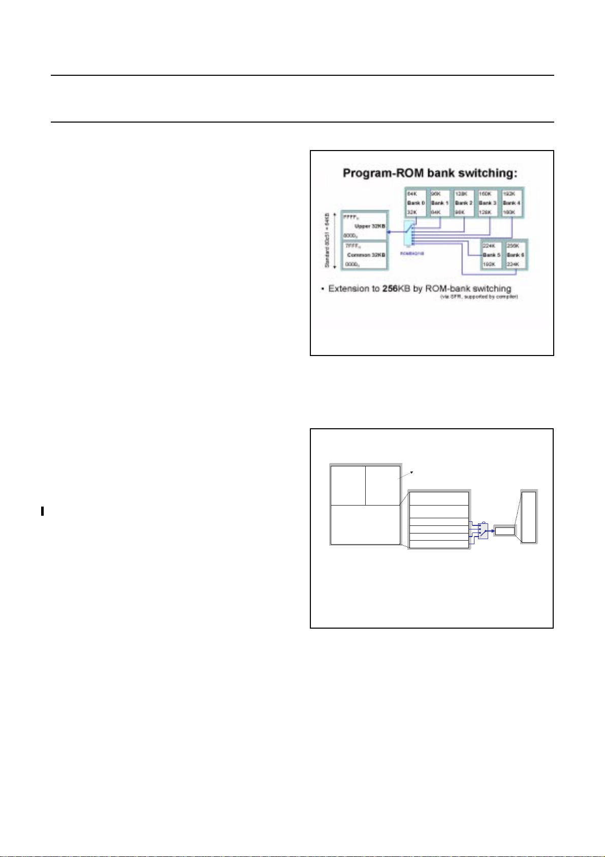
Fig.11 ROM Bank switching memory map
RAM Organisation
The Internal Data RAM is organised into two areas, Data
Memory and Special Function Registers (SFRs) as shown
in Fig.12.
Internal RAM : “I-Data”
FF
H
128B
RAM
only
Indirect
addressing
80
H
7F
H
Lower 128 Byte RAM
Direct
00
H
128B
only
Direct
addressing
&
Indirect
addressing
S
pecialFunctionRegisters
= extension method for 80c51
SFR
30..7F
20..2F
18..1FHRegister-Bank3
10..17HRegister-Bank2
08..0FHRegister-Bank1
00..07HRegister-Bank0
H
Bit-addressable
H
RAM
space
Register-Bank
select bits
in
PSW
R-Bank
R7
R6
R5
R4
R3
R2
R1
R0
Memory Organisation
Thedevice has the capability of a maximum of 256K Bytes
of PROGRAM ROM and 8K Bytes of AUX DATA RAM for
internally.
ROM Organisation
The 256K is arranged in eight banks of 32K. One of the
32K banks is common and is always addressable. The
other banks (Bank0 to Bank6) can be accessed by
selecting the right bank via the SFR ROMBK bits 2/1/0.
2003 Dec 18 29
CONFIDENTIAL
• Different addressing method for upper 128 Bytes
accesses RAM or SFR
Fig.12 Internal Data Memory
DATA MEMORY
TheDatamemory is 256 x 8-bits and occupies the address
range00 to FF Hex when using Indirect addressing and 00
to7F Hex when using direct addressing. The SFRs occupy
the address range 80 Hex to FF Hex and are accessible
using Direct addressing only. The lower 128 Bytes of Data
memory are mapped as shown in Fig.12. The lowest 32
bytes are grouped into 4 banks of 8 registers, the next 16
bytes above the register banks form a block of bit
addressable memory space. The upper 128 bytes are not
allocated for any special area or functions.

Philips Semiconductors Preliminary specification
Versatile signal processor for low- and
mid-range TV applications
SFR MEMORY
The Special Function Register (SFR) space is used for
port latches, counters/timers, peripheral control, data
capture and display control, etc. These registers can only
UOC
Sixteenoftheaddresses in the SFR space are both bit and
byte addressable. The bit addressable SFRs are those
whose address ends in 0H or 8H. A summary of the SFR
map in address order is shown in Table 5.
III
series
be accessed by direct addressing.
ADD R/W Names BIT7 BIT6 BIT5 BIT4 BIT3 BIT2 BIT1 BIT0
80H R/W P0 Reserved Reserved P0<5> P0<4> P0<3> P0<2> P0<1> P0<0>
81H R/W SP SP<7> SP<6> SP<5> SP<4> SP<3> SP<2> SP<1> SP<0>
82H R/W DPL DPL<7> DPL<6> DPL<5> DPL<4> DPL<3> DPL<2> DPL<1> DPL<0>
83H R/W DPH DPH<7> DPH<6> DPH<5> DPH<4> DPH<3> DPH<2> DPH<1> DPH<0>
84H R/W IEN1 - - - EX2 ERDS EUART ET2PR EBUSY
85H R/W IP1 - - - PX2 PRDS PUART PT2PR PBUSY
86H R/W RCP1 DAT<7> DAT<6> DAT<5> DAT<4> DAT<3> DAT<2> DAT<1> DAT<0>
87H R/W PCON SMOD ARD RFI WLE GF1 GF0 PD IDL
88H R/W TCON TF1 TR1 TF0 TR0 IE1 IT1 IE0 IT0
89H R/W TMOD GATE C/TM1 M0GATEC/TM1M0
8AH R/W TL0 TL0<7> TL0<6> TL0<5> TL0<4> TL0<3> TL0<2> TL0<1> TL0<0>
8BH R/W TL1 TL1<7> TL1<6> TL1<5> TL1<4> TL1<3> TL1<2> TL1<1> TL1<0>
8CH R/W TH0 TH0<7> TH0<6> TH0<5> TH0<4> TH0<3> TH0<2> TH0<1> TH0<0>
8DH R/W TH1 TH1<7> TH1<6> TH1<5> TH1<4> TH1<3> TH1<2> TH1<1> TH1<0>
8EH R RCP3 RA<7> RA<6> RA<5> RA<4> RA<3> RA<2> RA<1> RA<0>
8FH R RCP4 RB<11> RB<10> RB<9> RB<8> RA<11> RA<10> RA<9> RA<8>
90H R/W P1 P1<7> P1<6> P1<5> P1<4> P1<3> P1<2> P1<1> P1<0>
91H R/W TP2L TP2L<7> TP2L<6> TP2L<5> TP2L<4> TP2L<3> TP2L<2> TP2L<1> TP2L<0>
92H R/W TP2H TP2H<7> TP2H<6> TP2H<5> TP2H<4> TP2H<3> TP2H<2> TP2H<1> TP2H<0>
93H R/W TP2PR TP2PR<7> TP2PR<6> TP2PR<5> TP2PR<4> TP2PR<3> TP2PR<2> TP2PR<1> TP2PR<0>
94H R/W TP2CRL - - - - - - TP2CRL<1> TP2CRL<0>
95H R/W RCP2 - - - - DAT<11> DAT<10> DAT<9> DAT<8>
96H R/W P0CFGA Reserved Reserved P0CFGA<5> P0CFGA<4> P0CFGA<3> P0CFGA<2> P0CFGA<1> P0CFGA<0>
97H R/W P0CFGB Reserved Reserved P0CFGB<5> P0CFGB<4> P0CFGB<3> P0CFGB<2> P0CFGB<1> P0CFGB<0>
98H R/W SADB SSD_ON - - DC_COMP SAD<3> SAD<2> SAD<1> SAD<0>
99H R/W S0CON SM<0> SM<1> SM<2> REN TB8 RB8 TI RI
9AH R/W S0BUF S0BUF<7> S0BUF<6> S0BUF<5> S0BUF<4> S0BUF<3> S0BUF<2> S0BUF<1> S0BUF<0>
9BH R RCP5 RB<7> RB<6> RB<5> RB<4> RB<3> RB<2> RB<1> RB<0>
9CH R TP2CL TP2CL<7> TP2CL<6> TP2CL<5> TP2CL<4> TP2CL<3> TP2CL<2> TP2CL<1> TP2CL<0>
9DH R TP2CH TP2CH<7> TP2CH<6> TP2CH<5> TP2CH<4> TP2CH<3> TP2CH<2> TP2CH<1> TP2CH<0>
9EH R/W P1CFGA P1CFGA<7> P1CFGA<6> P1CFGA<5> P1CFGA<4> P1CFGA<3> P1CFGA<2> P1CFGA<1> P1CFGA<0>
9FH R/W P1CFGB P1CFGB<7> P1CFGB<6> P1CFGB<5> P1CFGB<4> P1CFGB<3> P1CFGB<2> P1CFGB<1> P1CFGB<0>
2003 Dec 18 30
CONFIDENTIAL
 Loading...