

Page 1

TZA3046
Fiber Channel/Gigabit Ethernet transimpedance amplifier
Rev. 01 — 19 May 2006 Product data sheet
1. General description
The TZA3046 is a transimpedance amplifier with AutomaticGainControl(AGC), designed
to be used in Fiber Channel/Gigabit Ethernet (FC/GE) fiber optic links. It amplifies the
current generated by a photo detector (PIN diode or avalanche photodiode) and converts
it to a differential output voltage. It offers a current mirror of average photo current for
RSSI monitoring to be used in SFF-8472 compliant modules.
The low noise characteristics makes it suitable for FC/GE applications, but also for
FTTx applications.
CAUTION
This device is sensitive to ElectroStatic Discharge (ESD). Therefore care should be taken
during transport and handling.
2. Features
n Low equivalent input noise current, typically 126 nA (RMS)
n Wide dynamic range, typically 2.5 µA to 1.7 mA (p-p)
n Differential transimpedance of 7.5 kΩ (typical)
n Bandwidth from DC to 1050 MHz (typical)
n Differential outputs
n On-chip AGC with possibility of external control
n Single supply voltage 3.3 V, range 2.97 V to 3.6 V
n Bias voltage for PIN diode
n On-chip current mirror of average photo current for RSSI monitoring
n Identical ports available on both sides of die for easy bond layout and RF polarity
3. Applications
n Digital fiber optic receiver modules in telecommunications transmission systems, in
selection
high-speed data networks or in FTTx systems.
Page 2
Philips Semiconductors
4. Ordering information
Table 1: Ordering information
Type number Package
TZA3046U - bare die, dimensions approximately
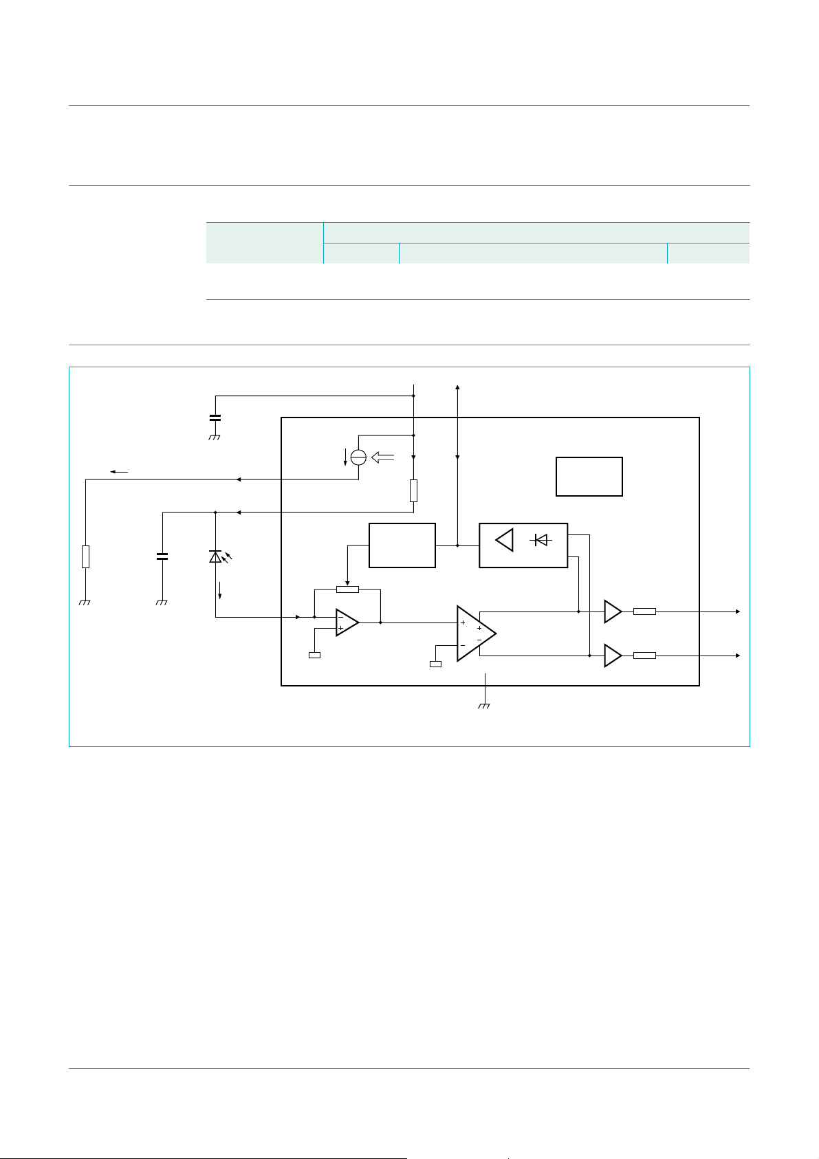
5. Block diagram
TZA3046
Fiber Channel/Gigabit Ethernet transimpedance amplifier
Name Description Version
-
0.82 mm × 1.3 mm
I
IDREF_MON
R
IDREF_MON
C
DREF
Fig 1. Block diagram
C
VCC
IDREF_MON
DREF
D
PHOTO
I
PIN
IPHOTO
0.2 × I
5 or 16
1 or 3
2
DREF
low noise
amplifier
R
DREF
GAIN
CONTROL
V
4 or 17
I
DREF
290 Ω
AGC
CC
6 or 15
PEAK DETECTOR
single-ended to
differential converter
9, 10, 11, 12
GND
BIASING
buffers
output
TZA3046
7 or 13
8 or 14
OUTQ
OUT
001aae511
TZA3046_1 © Koninklijke Philips Electronics N.V. 2006. All rights reserved.
Product data sheet Rev. 01 — 19 May 2006 2 of 15
Page 3
Philips Semiconductors
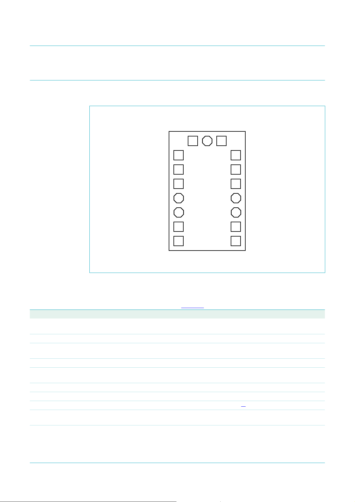
6. Pinning information
6.1 Pinning
TZA3046
Fiber Channel/Gigabit Ethernet transimpedance amplifier
DREF
IPHOTO
DREF
1
2
V
174
CC
IDREF_MON
165
AGC
156
OUT
14
OUTQ
13
129
GND
1110
GND
001aae512
V
CC
IDREF_MON
AGC
OUTQ
OUT
GND
GND
3
TZA3046
7
8
Fig 2. Pin configuration
6.2 Pin description
Table 2: Bonding pad description
Bonding pad locations with respect to the center of the die (see Figure 10); X and Y are inµm.
Symbol Pad X Y Type Description
DREF 1 −493.6 140 output bias voltage output for PIN diode; connect cathode of PIN diode to
pad 1 or pad 3
IPHOTO 2 −493.6 0 input current input; anode of PIN diode should be connected to this pad
DREF 3 −493.6 −140 output bias voltage output for PIN diode; connect cathode of PIN diode to
pad 1 or pad 3
V
CC
IDREF_MON 5 −213.6 −278.6 output current output for RSSI measurements; connect a resistor to pad 5
AGC 6 −73.6 −278.6 input AGC voltage; use pad 6 or pad 15
OUTQ 7 66.4 −278.6 output data output; complement of pad OUT; use pad 7 or pad 13
OUT 8 206.4 −278.6 output data output; use pad 8 or pad 14
GND 9 346.4 −278.6 ground ground; connect together pads 9, 10, 11 and pad 12 as many as
GND 10 486.4 −278.6 ground ground; connect together pads 9, 10, 11 and pad 12 as many as
4 −353.6 −278.6 supply supply voltage; connect supply voltage to pad 4 or pad 17
or pad 16 and ground
[1]
possible
possible
TZA3046_1 © Koninklijke Philips Electronics N.V. 2006. All rights reserved.
Product data sheet Rev. 01 — 19 May 2006 3 of 15
Page 4

Philips Semiconductors
TZA3046
Fiber Channel/Gigabit Ethernet transimpedance amplifier
Table 2: Bonding pad description
Bonding pad locations with respect to the center of the die (see Figure 10); X and Y are inµm.
Symbol Pad X Y Type Description
GND 11 486.4 278.6 ground ground; connect together pads 9, 10, 11 and pad 12 as many as
GND 12 346.4 278.6 ground ground; connect together pads 9, 10, 11 and pad 12 as many as
OUTQ 13 206.4 278.6 output data output; complement of pad OUT; use pad 7 or pad 13
OUT 14 66.4 278.6 output data output; use pad 8 or pad 14
AGC 15 −73.6 278.6 input AGC voltage; use pad 6 or pad 15
IDREF_MON 16 −213.6 278.6 output current output for RSSI measurements; connect a resistor to pad 5
V
CC
[1] These pads go HIGH when current flows into pad IPHOTO.
17 −353.6 278.6 supply supply voltage; connect supply voltage to pad 4 or pad 17
…continued
possible
possible
[1]
or pad 16 and ground
7. Functional description
The TZA3046 is a TransImpedance Amplifier (TIA) intended for use in fiber optic receivers
for signal recovery in FC/GE or FTTx applications. It amplifies the current generated by a
photo detector (PIN diode or avalanche photodiode) and converts it to a differentialoutput
voltage.
The most important characteristics of the TZA3046 are high receiver sensitivity, wide
dynamic range and large bandwidth. Excellent receiver sensitivity is achieved by
minimizing transimpedance amplifier noise.
The TZA3046 has a wide dynamic range to handle the signal current generated by the
PIN diode which can vary from 2.5 µA to 1.7 mA (p-p). This is implemented by an AGC
loop which reduces the preamplifier feedback resistance so that the amplifier remains
linear over the whole input range. The AGC loop hold capacitor is integrated on-chip, so
an external capacitor is not required.
The bandwidth of TZA3046 is optimized for FC/GE application. It works from DC onward
due to the absence of offset control loops. Therefore the amount of Consecutive Identical
Digits (CID) will not effect the output waveform. A differential amplifier converts the output
of the preamplifier to a differential voltage.
7.1 PIN diode connections
The performance of an optical receiver is largely determined by the combined effect of the
transimpedance amplifier and the PIN diode. In particular, the method used to connect the
PIN diode to the input (pad IPHOTO) and the layout around the input pad strongly
influences the main parameters of a transimpedance amplifier, such as sensitivity,
bandwidth, and PSRR.
Sensitivity is most affected by the value of the total capacitance at the input pad.
Therefore,to obtain the highest possible sensitivity the total capacitance should be as low
as possible.
TZA3046_1 © Koninklijke Philips Electronics N.V. 2006. All rights reserved.
Product data sheet Rev. 01 — 19 May 2006 4 of 15
Page 5
Philips Semiconductors
The parasitic capacitance can be minimized through:
1. Reducing the capacitance of the PIN diode. This is achieved by proper choice of PIN
diode and typically a high reverse voltage.
2. Reducing the parasitics around the input pad. This is achieved by placing the PIN
diode as close as possible to the TIA.
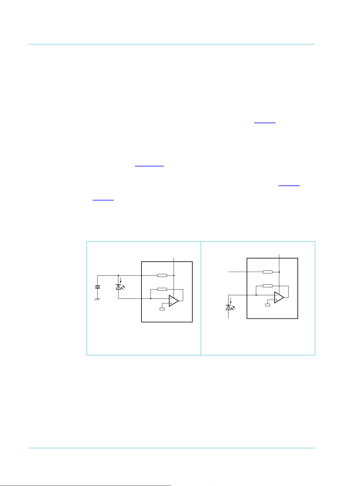
The PIN diode can be biased with a positive or a negative voltage.Figure 3 shows the PIN
diode biased positively, using the on-chip bias pad DREF. The voltage at DREF is derived
from VCCby a low-pass filter comprising internal resistor R
which decouples any supply voltage noise. The value of external capacitor C2 affects the
value of PSRR and should have a minimum value of 470 pF. Increasing this value
improves the value of PSRR. The current through R
IDREF_MON, see Section 7.3.
If the biasing for the PIN diode is done external to the IC, pad DREF can be left
unconnected. If a negative bias voltage is used, the configuration shown in Figure 4 can
be used. In this configuration, the direction of the signal current is reversed to that shown
in Figure 3. It is essential that in these applications, the PIN diode bias voltage is filtered to
achieve the best sensitivity.
TZA3046
Fiber Channel/Gigabit Ethernet transimpedance amplifier
and external capacitor C2
DREF
is measured and sourced at pad
DREF
For maximum freedom on bonding location, 2 outputs are available for DREF (pads 1
and 3). These are internally connected. Both outputs can be used if necessary. If only one
is used, the other can be left open.
V
R
DREF
290 Ω
TZA3046
CC
4 or 17
001aae514
V
CC
4 or 17
R
DREF
1 or 3
DREF
C2
470 pF
I
PIN
IPHOTO
290 Ω
2
TZA3046
001aae513
Fig 3. The PIN diode connected between
the input and pad DREF
1 or 3
DREF
IPHOTO
negative
bias voltage
2
I
PIN
Fig 4. The PIN diode connected between
the input and a negative supply
voltage
TZA3046_1 © Koninklijke Philips Electronics N.V. 2006. All rights reserved.
Product data sheet Rev. 01 — 19 May 2006 5 of 15
Page 6

Philips Semiconductors
7.2 Automatic gain control
The TZA3046 transimpedance amplifier can handle input currents from 2.5 µA to 1.7 mA
which is equivalent to a dynamic range of 56 dB (electrical equivalent with 28 dB optical).
At low input currents, the transimpedance must be high to obtain enough output voltage,
and the noise should be low enough to guarantee a minimum bit error rate. At high input
currents however,thetransimpedanceshouldbelowtoprevent excessive distortion at the
output stage. To achieve the dynamic range, the gain of the amplifier depends on the level
of the input signal. This is achieved in the TZA3046 by an AGC loop.
The AGC loop comprises a peak detector and a gain control circuit. The peak detector
detects the amplitude of the signal and stores it in a hold capacitor. The hold capacitor
voltage is compared to a threshold voltage. The AGC is only active when the input signal
level is larger than the threshold level and is inactive when the input signal is smaller than
the threshold level.
When the AGC is inactive, the transimpedance is at its maximum. When the AGC is
active,thefeedbackresistorvalueofthetransimpedanceamplifieris reduced, reducing its
transimpedance, to keepthe output voltage constant. Figure 5 shows the transimpedance
as function of the input current.
TZA3046
Fiber Channel/Gigabit Ethernet transimpedance amplifier
To reduce sensitivity to offsets and output loads, the AGC detector senses the output just
before the output buffer. Figure 6 shows the AGC voltage as function of the input current.
10
001aae515
3
I
PIN
4
(µA)
10
transimpedance
(kΩ)
1
−1
10
110
10 10
2
Fig 5. Transimpedance as function of the PIN diode
current
10
001aae516
3
I
PIN
(µA)
3.5
V
AGC
(V)
2.5
1.5
0.5
110
10 10
2
Fig 6. AGC voltage as function of the PIN diode
current
4
TZA3046_1 © Koninklijke Philips Electronics N.V. 2006. All rights reserved.
Product data sheet Rev. 01 — 19 May 2006 6 of 15
Page 7

Philips Semiconductors
For applications where the transimpedance is controlled by the TIA it is advised to leave
the AGC pads unconnected to achieve fast attack and decay times.
The AGC function can be overruled by applying a voltage to pad AGC. In this
configuration, connecting pad AGC to ground gives maximum transimpedance and
connecting it to VCC gives minimum transimpedance. This is depicted in Figure 7. The
AGC voltage should be derived from the VCC for proper functioning.
Formaximum freedom on bonding location, 2 pads are availablefor AGC (pads 6 and 15).
These pads are internally connected. Both pads can be used if necessary.
TZA3046
Fiber Channel/Gigabit Ethernet transimpedance amplifier
10
transimpedance
(kΩ)
1
−1
10
0.3 0.90.70.5
Fig 7. Transimpedance as function of the AGC voltage
001aae517
V
AGC/VCC
7.3 Monitoring RSSI via IDREF_MON
To facilitate RSSI monitoring in modules (e.g. SFF-8472 compliant SFP modules), a
current output is provided. This output gives a current which is 20 % of the average DREF
current through the 290 Ω bias resistor. By connecting a resistor to the IDREF_MON
output, a voltage proportional to the average input power can be obtained.
The RSSI monitoring is implemented by measuring the voltage over the 290 Ω bias
resistor. This method is preferred over a simple current mirror because at small photo
currents the voltage drop over the resistor is very small. This gives a higher bias voltage
yielding better performance of the photodiode.
For maximum freedom on bonding location, 2 pads are available for IDREF_MON (pads 5
and 16). These pads are internally connected. Both pads can be used if necessary. If only
one is used, the other can be left open.
TZA3046_1 © Koninklijke Philips Electronics N.V. 2006. All rights reserved.
Product data sheet Rev. 01 — 19 May 2006 7 of 15
Page 8

Philips Semiconductors
8. Limiting values
Table 3: Limiting values
In accordance with the Absolute Maximum Rating System (IEC 60134).
Symbol Parameter Conditions Min Max Unit
V
CC
V
n
I
n
P
tot
T
amb
T
j
T
stg
TZA3046
Fiber Channel/Gigabit Ethernet transimpedance amplifier
supply voltage −0.5 +3.8 V
voltage on any other
pin
current on any other
pin
total power dissipation - 300 mW
ambient temperature −40 +85 °C
junction temperature - 150 °C
storage temperature −65 +150 °C
pad
IPHOTO −0.5 +2.0 V
OUT, OUTQ −0.5 V
AGC, IDREF_MON −0.5 V
DREF −0.5 V
+ 0.5 V
CC
+ 0.5 V
CC
+ 0.5 V
CC
pad
IPHOTO −4.0 +4.0 mA
OUT, OUTQ −10 +10 mA
AGC, IDREF_MON −0.2 +0.2 mA
DREF −4.0 +4.0 mA
9. Characteristics
Table 4: Characteristics
Typical values at Tj=25°C and VCC= 3.3 V; minimum and maximum values are valid over the entire ambient temperature
range and supply voltage range; all voltages are measured with respect to ground; unless otherwise specified.
Symbol Parameter Conditions Min Typ Max Unit
V
CC
I
CC
P
tot
T
j
T
amb
R
tr
f
-3dB(h)
I
n(rms)(itg)(tot)
Automatic gain control loop: pad AGC
t
att
t
decay
V
th(AGC)(p-p)
supply voltage 2.97 3.3 3.6 V
supply current AC-coupled; R
excluding I
DREF
L(dif)
and I
= 100 Ω;
IDREF_MON
-21 23 mA
total power dissipation VCC= 3.3 V - 70 76 mW
junction temperature −40 - +125 °C
ambient temperature −40 +25 +85 °C
small-signal
transresistance
high frequency
measured differentially;
AC-coupled, R
C
= 0.5 pF 800 1050 - MHz
PIN
L(dif)
= 100 Ω
5.5 7.5 10.5 kΩ
−3 dB point
totalintegratedRMS noise
current over bandwidth
referenced to input;
C
= 0.5 pF;
PIN
f
-3dB(min)
= 875 MHz
[1]
- 126 164 nA
attack time AGC pad unconnected - 14 - µs
decay time AGC pad unconnected - 40 - µs
peak-to-peak AGC
threshold voltage
referenced to output;
measured differentially
- 125 - mV
TZA3046_1 © Koninklijke Philips Electronics N.V. 2006. All rights reserved.
Product data sheet Rev. 01 — 19 May 2006 8 of 15
Page 9

Philips Semiconductors
TZA3046
Fiber Channel/Gigabit Ethernet transimpedance amplifier
Table 4: Characteristics
…continued
Typical values at Tj=25°C and VCC= 3.3 V; minimum and maximum values are valid over the entire ambient temperature
range and supply voltage range; all voltages are measured with respect to ground; unless otherwise specified.
Symbol Parameter Conditions Min Typ Max Unit
Bias voltage: pad DREF
R
(DREF-VCC)
TC
RDREF
resistance between pin
DREF and pin V
CC
temperature coefficient of
R
DREF
tested at DC level;
T
=25°C
amb
260 290 320 Ω
- 0.33 - Ω/°C
Input: pad IPHOTO
I
IPHOTO(p-p)
peak-to-peak current on
[2][3]
−1000 +1700 - µA
pad IPHOTO
V
bias(i)
input bias voltage 700 850 1000 mV
Monitor: pad IDREF_MON
V
mon
I
IDREF_MON/IDREF
I
offset(mon)
TC
I(offset)mon
monitor voltage 0 - VCC− 0.4 V
monitor current ratio ratio I
monitor offset current T
amb
temperature coefficient of
IDREF_MON
=25°C 0 10 20 µA
/ I
DREF
19.5 20 20.5 %
- 30 - nA/°C
monitor offset current
Data outputs: pads OUT and OUTQ
V
O(cm)
common mode output
AC-coupled; R
= 100 Ω -VCC− 1.2 - V
L(dif)
voltage
V
o(dif)(p-p)
R
O(dif)
peak-to-peak differential
output voltage
differential output
AC-coupled; R
= 2.5 µA (p-p) × R
I
PIN
= 100 µA (p-p) - 120 - mV
I
PIN
= 1500 µA (p-p)
I
PIN
L(dif)
= 100 Ω
tr
14 19 - mV
[4]
- 325 600 mV
tested at DC level - 100 - Ω
resistance
t
r
t
f
rise time 20 % to 80 %;
I
= 100 µA (p-p)
PIN
fall time 80% to 20 %;
I
= 100 µA (p-p)
PIN
- 150 - ps
- 150 - ps
[1] Guaranteed by design.
amb
−10
= 25°
[2] Max input current is guaranteed for BER < 10
[3] Max input current is guaranteed for T
[4] Max value of 500 mV belongs to I
TZA3046_1 © Koninklijke Philips Electronics N.V. 2006. All rights reserved.
Product data sheet Rev. 01 — 19 May 2006 9 of 15
= 1250 µA (p-p)
PIN
Page 10

Philips Semiconductors
10. Application information
For maximum freedom on bonding location, 2 outputs are available for OUT and OUTQ.
The outputs should be used in pairs: pad 14 with pad 7 or pad 8 with pad 13. Pad 8 is
internally connected with pad 14, pad 7 is internally connected with pad 13. The device is
guaranteed with only one pair used. The other pair should be left open. Two examples of
the bonding possibilities are shown in Figure 8.
TZA3046
Fiber Channel/Gigabit Ethernet transimpedance amplifier
V
C
CC
OUT
PIN
TZA3046U
GND
IDREF_MON
C
OUTQ
Fig 8. Application diagram highlighting flexible pad lay out
IDREF_MON
OUTQ
C
PIN
TZA3046U
GND
V
CC
OUT
C
001aae518
TZA3046_1 © Koninklijke Philips Electronics N.V. 2006. All rights reserved.
Product data sheet Rev. 01 — 19 May 2006 10 of 15
Page 11

TZA3046_1 © Koninklijke Philips Electronics N.V. 2006. All rights reserved.
Product data sheet Rev. 01 — 19 May 2006 11 of 15
xxxx xxxxxxxxxxxxxxxxxxxxxxxxxxxxxx x xxxxxxxxxxxxxx xxxxxxxxxx xxx xxxxxx xxxxxxxxxxxxxxxxxxxxxxx xxxxxxxxxxxxxxxxxxxxxx
xxxxx xxxxxx xx xxxxxxxxxxxxxxxxxxxxxxxxxxxxx xxxxxxxxxxxxxxxxxxxxxx xxxxxxxxxxx xxxxxxx xxxxxxxxxxxxxxxxxxx
xxxxxxxxxxxxxxxx xxxxxxxxxxxxxx xxxxxx xx xxxxxxxxxxxxxxxxxxxxxxxxxxxxxxxx xxxxxxxxxxxxxxxxxxxxxxxx xxxxxxx
xxxxxxxxxxxxxxxxxxxxxxxxxxxxxxxxxxxxxxxxxxxxxx xxxxxxxxxxx xxxxx x x
NETWORK ANALYZER
S-PARAMETER TEST SET
PATTERN
GENERATOR
CLOCK
DATA
DC-IN
22 nF
55 Ω
8.2
PORT1
V
CC
4 or 17
OUT
8 or 14
kΩ
330 Ω
IPHOTO
R
TZA3046
2
9, 10, 11, 12
7 or 13
GND
OUTQ
22 nF
22 nF
PORT2
Z
= 50 ΩZo = 50 Ω
o
SAMPLING OSCILLOSCOPE
Z
= 50 Ω
o
21
TRIGGER
INPUT
11. Test information
Fiber Channel/Gigabit Ethernet transimpedance amplifier
Philips Semiconductors
Total impedance of the test circuit (Z
Typical values: R = 330 Ω, Zi=30Ω.
Fig 9. Test circuit
) is calculated by the equation Z
tot(tc)
tot(tc)=s21
001aae519
TZA3046
× (R+Zi) × 2, where s21 is the insertion loss of ports 1 and 2.
Page 12

Philips Semiconductors
12. Bare die information
TZA3046
Fiber Channel/Gigabit Ethernet transimpedance amplifier
17 16 15 14 13 12 11
1
2
3
456
Origin is center of die.
Y
X
(0,0)
78910
001aac627
Fig 10. Bonding pad locations
Table 5: Physical characteristics of the bare die
Parameter Value
Glass passivation 0.3 µm PSG (PhosphoSilicate Glass) on top of 0.8 µm silicon nitride
Bonding pad
dimension
minimum dimension of exposed metallization is 90 µm × 90 µm
(pad size = 100 µm × 100 µm) except pads 2 and 3 which have exposed
metallization of 80 µm × 80 µm (pad size = 90 µm × 90 µm)
Metallization 2.8 µm AlCu
Thickness 380 µm nominal
2
Die dimension 820 µm × 1300 µm (± 20 µm
)
Backing silicon; electrically connected to GND potential through substrate contacts
Attach temperature < 440 °C; recommended die attach is glue
Attach time < 15 s
13. Package outline
Not applicable.
TZA3046_1 © Koninklijke Philips Electronics N.V. 2006. All rights reserved.
Product data sheet Rev. 01 — 19 May 2006 12 of 15
Page 13

Philips Semiconductors
14. Handling information
14.1 General
Inputs and outputs are protected against electrostatic discharge in normal handling.
However, to be completely safeyou must take normal precautions appropriate to handling
MOS devices; see
14.2 Additional information
Pad IPHOTO has limited protection to ensure good RF performance. This pad should be
handled with extreme care.
15. Abbreviations
Table 6. Abbreviations
Acronym Description
BER Bit Error Rate
FTTx Fiber To The “x”
OC3 Optical Carrier level 3 (155.52 Mbit/s)
PIN Positive Intrinsic Negative
PSRR Power Supply Rejection Ratio
RSSI Received Signal Strength Indicator
SDH Synchronous Digital Hierarchy
SFP Small Form-factor Pluggable
SONET Synchronous Optical NETwork
STM1 Synchronous Transport Module 1 (155.52 Mbit/s
Fiber Channel/Gigabit Ethernet transimpedance amplifier
JESD625-A and/or IEC61340-5
TZA3046
.
16. Revision history
Table 7. Revision history
Document ID Release date Data sheet status Change notice Supersedes
TZA3046_1 20060519 Product data sheet - -
TZA3046_1 © Koninklijke Philips Electronics N.V. 2006. All rights reserved.
Product data sheet Rev. 01 — 19 May 2006 13 of 15
Page 14

Philips Semiconductors
17. Legal information
17.1 Data sheet status
TZA3046
Fiber Channel/Gigabit Ethernet transimpedance amplifier
Document status
Objective [short] data sheet Development This document contains data from the objective specification for product development.
Preliminary [short] data sheet Qualification This document contains data from the preliminary specification.
Product [short] data sheet Production This document contains the product specification.
[1] Please consult the most recently issued document before initiating or completing a design.
[2] The term ‘short data sheet’ is explained in section “Definitions”.
[3] Theproduct status of device(s) described in this document may have changed since this document was published and may differin case of multiple devices. The latest product status
information is available on the Internet at URL
[1][2]
Product status
17.2 Definitions
Draft — The document is a draft version only. The content is still under
internal review and subject to formal approval, which may result in
modifications or additions. Philips Semiconductors does not give any
representations or warranties as to the accuracy or completeness of
information included herein and shall haveno liability for the consequences of
use of such information.
Short data sheet — A short data sheet is an extract from a full data sheet
with the same product type number(s)and title. A short data sheet isintended
for quick referenceonly and should not be relied upon to contain detailed and
full information. For detailed and full information see the relevant full data
sheet, which is available on request via the local Philips Semiconductors
sales office. In case of any inconsistency or conflict with the short data sheet,
the full data sheet shall prevail.
17.3 Disclaimers
General — Information in this document is believed to be accurate and
reliable. However, Philips Semiconductors does not give any representations
or warranties, expressed or implied, as to the accuracy or completeness of
such information and shall have no liability for the consequences of use of
such information.
Right to make changes — Philips Semiconductors reserves the right to
make changes to information published in this document, including without
limitation specifications and product descriptions, at any time and without
notice. This document supersedes and replaces all information supplied prior
to the publication hereof.
Suitability for use — Philips Semiconductors products are not designed,
authorized or warranted to be suitable for use in medical, military, aircraft,
space or life support equipment, nor in applications where failure or
malfunction of a Philips Semiconductors product can reasonably be expected
to result in personal injury, death or severe property or environmental
damage. Philips Semiconductors accepts no liability for inclusion and/or use
of Philips Semiconductors products in such equipment or applications and
therefore such inclusion and/or use is for the customer’s own risk.
Applications — Applications that are described herein for any of these
products are for illustrative purposes only. Philips Semiconductors makes no
representation or warranty that such applications will be suitable for the
specified use without further testing or modification.
[3]
http://www.semiconductors.philips.com.
Definition
Limiting values — Stress above one or more limiting values (as defined in
the Absolute Maximum Ratings System of IEC 60134) may cause permanent
damage to the device. Limiting values are stress ratings only and and
operation of the device at these or any other conditions above those given in
the Characteristics sections of this document is not implied. Exposure to
limiting values for extended periods may affect device reliability.
Terms and conditions of sale — Philips Semiconductors products are sold
subject to the general terms and conditions of commercial sale, as published
at
http://www.semiconductors.philips.com/profile/terms, including those
pertaining to warranty, intellectual property rights infringement and limitation
of liability, unless explicitly otherwise agreed to in writing by Philips
Semiconductors. In case of any inconsistency or conflict between information
in this document and such terms and conditions, the latter will prevail.
No offer to sell or license — Nothing in this document may be interpreted
or construed as an offer to sell products that is open for acceptance or the
grant, conveyanceor implication of any license under any copyrights, patents
or other industrial or intellectual property rights.
Bare die — All die are tested on compliance with all related technical
specifications as stated in this data sheet up to the point of wafer sawing for a
period of ninety (90) days from the date of delivery by Philips
Semiconductors. If there are data sheet limits not guaranteed, these will be
separately indicated in the data sheet. There are no post-packing tests
performed on individual die or wafers.
Philips Semiconductors has no control of third party procedures in the
sawing, handling, packing or assembly of the die. Accordingly, Philips
Semiconductors assumes no liability for device functionality or performance
of the die or systems after third party sawing, handling, packing or assembly
of the die. It is the responsibility of the customer to test and qualify their
application in which the die is used.
All die sales are conditioned upon and subject to the customer entering into a
written die sale agreement with Philips Semiconductors through its legal
department.
17.4 Trademarks
Notice: All referencedbrands, product names, service names and trademarks
are the property of their respective owners.
18. Contact information
For additional information, please visit: http://www.semiconductors.philips.com
For sales office addresses, send an email to: sales.addresses@www.semiconductors.philips.com
TZA3046_1 © Koninklijke Philips Electronics N.V. 2006. All rights reserved.
Product data sheet Rev. 01 — 19 May 2006 14 of 15
Page 15

Philips Semiconductors
Fiber Channel/Gigabit Ethernet transimpedance amplifier
19. Contents
1 General description . . . . . . . . . . . . . . . . . . . . . . 1
2 Features . . . . . . . . . . . . . . . . . . . . . . . . . . . . . . . 1
3 Applications . . . . . . . . . . . . . . . . . . . . . . . . . . . . 1
4 Ordering information. . . . . . . . . . . . . . . . . . . . . 2
5 Block diagram . . . . . . . . . . . . . . . . . . . . . . . . . . 2
6 Pinning information. . . . . . . . . . . . . . . . . . . . . . 3
6.1 Pinning . . . . . . . . . . . . . . . . . . . . . . . . . . . . . . . 3
6.2 Pin description . . . . . . . . . . . . . . . . . . . . . . . . . 3
7 Functional description . . . . . . . . . . . . . . . . . . . 4
7.1 PIN diode connections . . . . . . . . . . . . . . . . . . . 4
7.2 Automatic gain control . . . . . . . . . . . . . . . . . . . 6
7.3 Monitoring RSSI via IDREF_MON . . . . . . . . . . 7
8 Limiting values. . . . . . . . . . . . . . . . . . . . . . . . . . 8
9 Characteristics. . . . . . . . . . . . . . . . . . . . . . . . . . 8
10 Application information. . . . . . . . . . . . . . . . . . 10
11 Test information. . . . . . . . . . . . . . . . . . . . . . . . 11
12 Bare die information . . . . . . . . . . . . . . . . . . . . 12
13 Package outline . . . . . . . . . . . . . . . . . . . . . . . . 12
14 Handling information. . . . . . . . . . . . . . . . . . . . 13
14.1 General. . . . . . . . . . . . . . . . . . . . . . . . . . . . . . 13
14.2 Additional information . . . . . . . . . . . . . . . . . . . 13
15 Abbreviations. . . . . . . . . . . . . . . . . . . . . . . . . . 13
16 Revision history. . . . . . . . . . . . . . . . . . . . . . . . 13
17 Legal information. . . . . . . . . . . . . . . . . . . . . . . 14
17.1 Data sheet status . . . . . . . . . . . . . . . . . . . . . . 14
17.2 Definitions. . . . . . . . . . . . . . . . . . . . . . . . . . . . 14
17.3 Disclaimers . . . . . . . . . . . . . . . . . . . . . . . . . . . 14
17.4 Trademarks. . . . . . . . . . . . . . . . . . . . . . . . . . . 14
18 Contact information. . . . . . . . . . . . . . . . . . . . . 14
19 Contents . . . . . . . . . . . . . . . . . . . . . . . . . . . . . . 15
TZA3046
Please be aware that important notices concerning this document and the product(s)
described herein, have been included in section ‘Legal information’.
© Koninklijke Philips Electronics N.V. 2006. All rights reserved.
For more information, please visit: http://www.semiconductors.philips.com.
For sales office addresses, email to: sales.addresses@www.semiconductors.philips.com.
Date of release: 19 May 2006
Document identifier: TZA3046_1
 Loading...