

Philips TZA3043T, TZA3043U Datasheet

INTEGRATED CIRCUITS
DATA SH EET
TZA3043
Gigabit Ethernet/Fibre Channel
transimpedance amplifier
Objective specification
File under Integrated Circuits, IC19
1998 Jul 08
Philips Semiconductors Objective specification
Gigabit Ethernet/Fibre Channel transimpedance amplifier TZA3043
FEATURES
• Wide dynamic range, typically 2.5 µA to 1.5 mA
• Differential transimpedance of 14 kΩ
• Wide bandwidth of 950 MHz
• Differential outputs
• On-chip AGC (Automatic Gain Control)
• No external components required
• Single supply voltage from 3.0 to 5.5 V
• Bias voltage for PIN diode
• Pin compatible with TZA3023 and SA5223.
APPLICATIONS
• Digital fibre optic receiver in medium and long haul
optical telecommunications transmission systems or in
high speed data networks
• Wideband RF gain block.
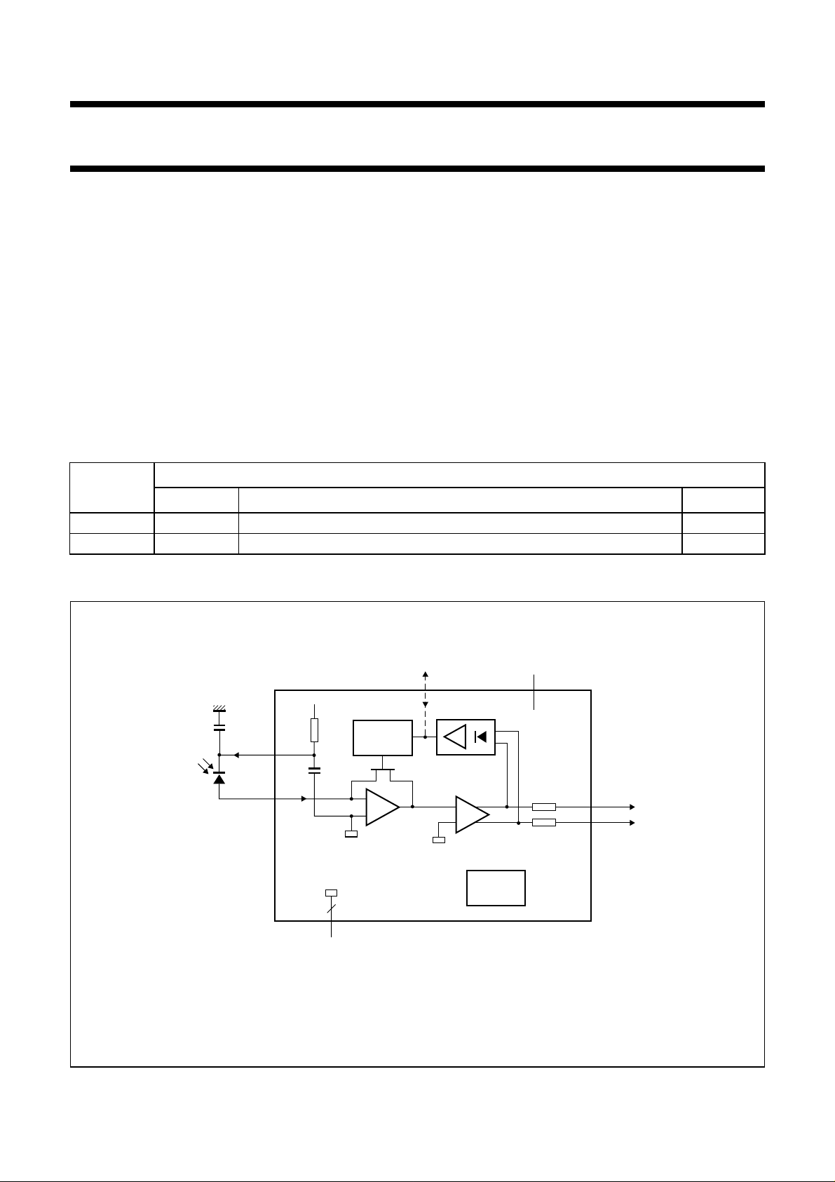
DESCRIPTION
The TZA3043 is a high speed transimpedance amplifier
with AGC designed to be used in Gigabit Ethernet/Fibre
Channel optical links. It amplifies the current generated by
a photo detector (PIN diode or avalanche photodiode) and
converts it to a differential output voltage.
ORDERING INFORMATION
TYPE
NUMBER
NAME DESCRIPTION VERSION
PACKAGE
TZA3043T SO8 plastic small outline package; 8 leads; body width 3.9 mm SOT96-1
TZA3043U naked die die in waffle pack carriers; die dimensions 0.960 × 1.210 mm −
BLOCK DIAGRAM
handbook, full pagewidth
V
CC
1 nF
1 (1)
DREF
3 (4)IPhoto
(1) AGC analog I/O is only available on the TZA3043U (pad 13).
The numbers in brackets refer to the pad numbers of the naked die version.
2 kΩ
10 pF
3
GND
GAIN
CONTROL
A1
low noise
TZA3043
2, 4, 5 (2, 3, 5, 6, 7, 8)
Fig.1 Block diagram.
(1)
AGC
peak detector
A2
amplifier single-ended to
differential converter
BIASING
V
CC
8 (11, 12)(13)
(10) 7 OUTQ
(9) 6 OUT
MGR286
1998 Jul 08 2
Philips Semiconductors Objective specification
Gigabit Ethernet/Fibre Channel transimpedance amplifier TZA3043
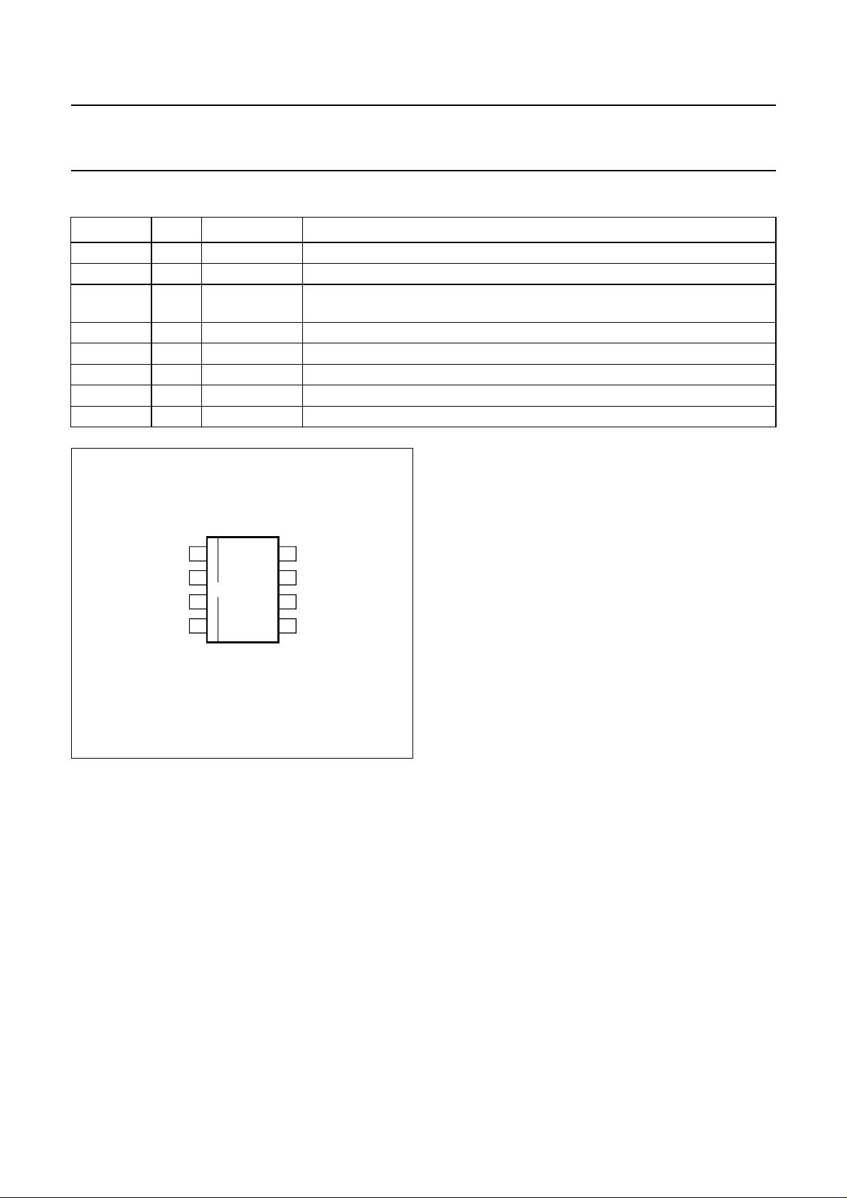
PINNING
SYMBOL PIN TYPE DESCRIPTION
DREF 1 analog output bias voltage for PIN diode (V
GND 2 ground ground
IPhoto 3 analog input current input; anode of PIN diode should be connected to this pin; DC bias
level of 822 mV is one diode voltage above ground
GND 4 ground ground
GND 5 ground ground
OUT 6 data output data output; OUT goes HIGH when current flows into IPhoto (pin 3)
OUTQ 7 data output compliment of OUT (pin6)
V
CC
8 supply supply voltage
); cathode should be connected to this pin
CC
handbook, halfpage
DREF
1
2
TZA3043T
3
IPhoto
4
GND
MGR287
Fig.2 Pin configuration.
V
8
CC
OUTQGND
7
OUT
6
GND
5
1998 Jul 08 3
Philips Semiconductors Objective specification
Gigabit Ethernet/Fibre Channel transimpedance amplifier TZA3043
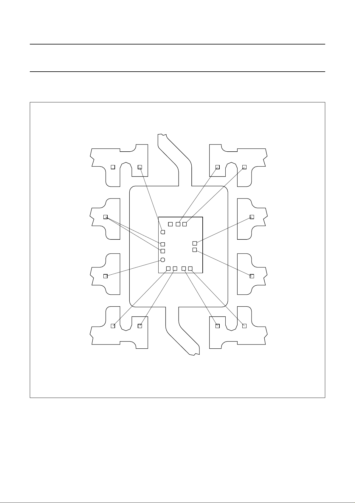
PAD CONFIGURATION
Bonding pad locations
handbook, full pagewidth
18
DREF
V
CC
GND
IPhoto
GND
Pad 13 (AGC) is not bonded.
2
36
AGC
12
13
1
2
TZA3043U
3
4
5
67
7
OUTQ
11
10
9
8
OUT
GND
45
MGR288
Fig.3 Bonding diagram TZA3043U.
1998 Jul 08 4
 Loading...