

Philips TZA3043B, TZA3043 Datasheet

INTEGRATED CIRCUITS
DATA SH EET
TZA3043; TZA3043B
Gigabit Ethernet/Fibre Channel
transimpedance amplifier
Product specification
Supersedes data of 1998 Jul 08
File under Integrated Circuits, IC19
2000 Mar 28
Philips Semiconductors Product specification
Gigabit Ethernet/Fibre Channel
TZA3043; TZA3043B
transimpedance amplifier
FEATURES
• Wide dynamic range, typically 2.5 µA to 1.5 mA
• Low equivalent input noise, typically 5.7 pA/√Hz
• Differential transimpedance of 8.3 kΩ
• Wide bandwidth from DC to 950 MHz
• Differential outputs
• On-chip Automatic Gain Control (AGC)
• No external components required
• Single supply voltage from 3.0 to 5.5 V
• Bias voltage for PIN diode
• Pin compatible with TZA3023 and SA5223
• Switched output polarity available (B-version).
ORDERING INFORMATION
TYPE
NUMBER
TZA3043T SO8 plastic small outline package; 8 leads; body width 3.9 mm SOT96-1
TZA3043U − bare die in waffle pack carriers; die dimensions 1.030 × 1.300 mm −
TZA3043BT SO8 plastic small outline package; 8 leads; body width 3.9 mm SOT96-1
TZA3043BU − bare die in waffle pack carriers; die dimensions 1.030 × 1.300 mm −
NAME DESCRIPTION VERSION
APPLICATIONS
• Digital fibre optic receiver in medium and long haul
optical telecommunications transmission systems or in
high speed data networks
• Wideband RF gain block.
GENERAL DESCRIPTION
The TZA3043 is a high speed transimpedance amplifier
with AGC designed to be used in Gigabit Ethernet/Fibre
Channel opticallinks. It amplifies the current generated by
a photo detector (PIN diode or avalanchephotodiode) and
converts it to a differential output voltage.
PACKAGE
2000 Mar 28 2
Philips Semiconductors Product specification
Gigabit Ethernet/Fibre Channel
transimpedance amplifier
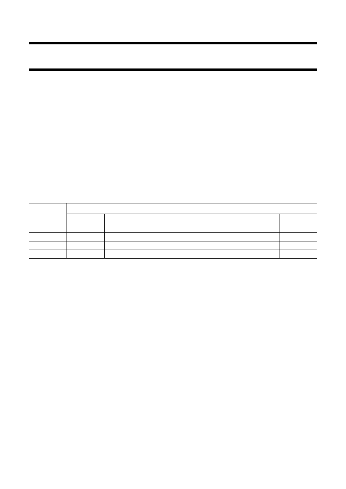
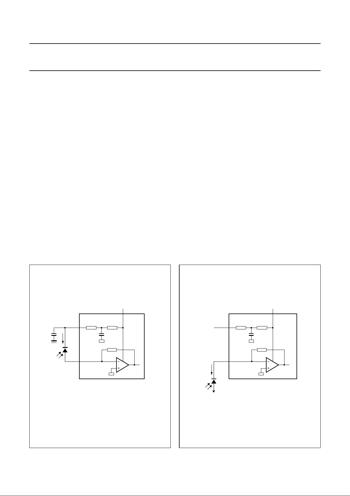
BLOCK DIAGRAM
handbook, full pagewidth
V
CC
1 nF
125 Ω
1 (1)
DREF
3 (4)IPhoto
TZA3043T
TZA3043U
125 Ω
10 pF
GND
GAIN
CONTROL
A1
low noise
amplifier single-ended to
2, 4, 5 (2, 3, 5, 6, 7, 8)
(1)
AGC
peak detector
differential converter
A2
BIASING
TZA3043; TZA3043B
V
CC
8 (11, 12)(13)
(10) 7 OUTQ
(9) 6 OUT
MGU096
The numbers in brackets refer to the pad numbers of the bare die version.
(1) AGC analog I/O (pad 13) is only available on the TZA3043U.
Fig.1 Block diagram of TZA3043T and TZA3043U.
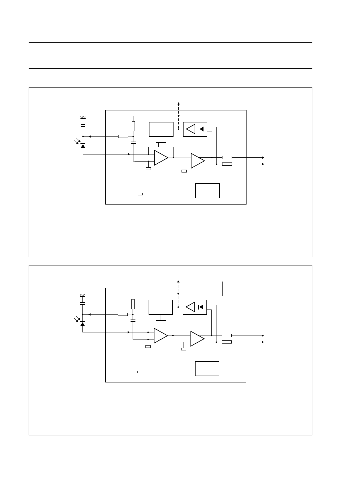
handbook, full pagewidth
V
CC
1 nF
DREF
125 Ω
1 (1)
3 (4)IPhoto
TZA3043BT
TZA3043BU
125 Ω
CONTROL
10 pF
2, 4, 5 (2, 3, 5, 6, 7, 8)
GND
(1)
AGC
GAIN
peak detector
A1
low noise
amplifier single-ended to
A2
differential converter
BIASING
V
CC
8 (11, 12)(13)
(9) 6
OUTQ
(10) 7
OUT
MGU097
The numbers in brackets refer to the pad numbers of the bare die version.
(1) AGC analog I/O (pad 13) is only available on the TZA3043BU.
Fig.2 Block diagram of TZA3043BT and TZA3043BU.
2000 Mar 28 3
Philips Semiconductors Product specification
Gigabit Ethernet/Fibre Channel
transimpedance amplifier
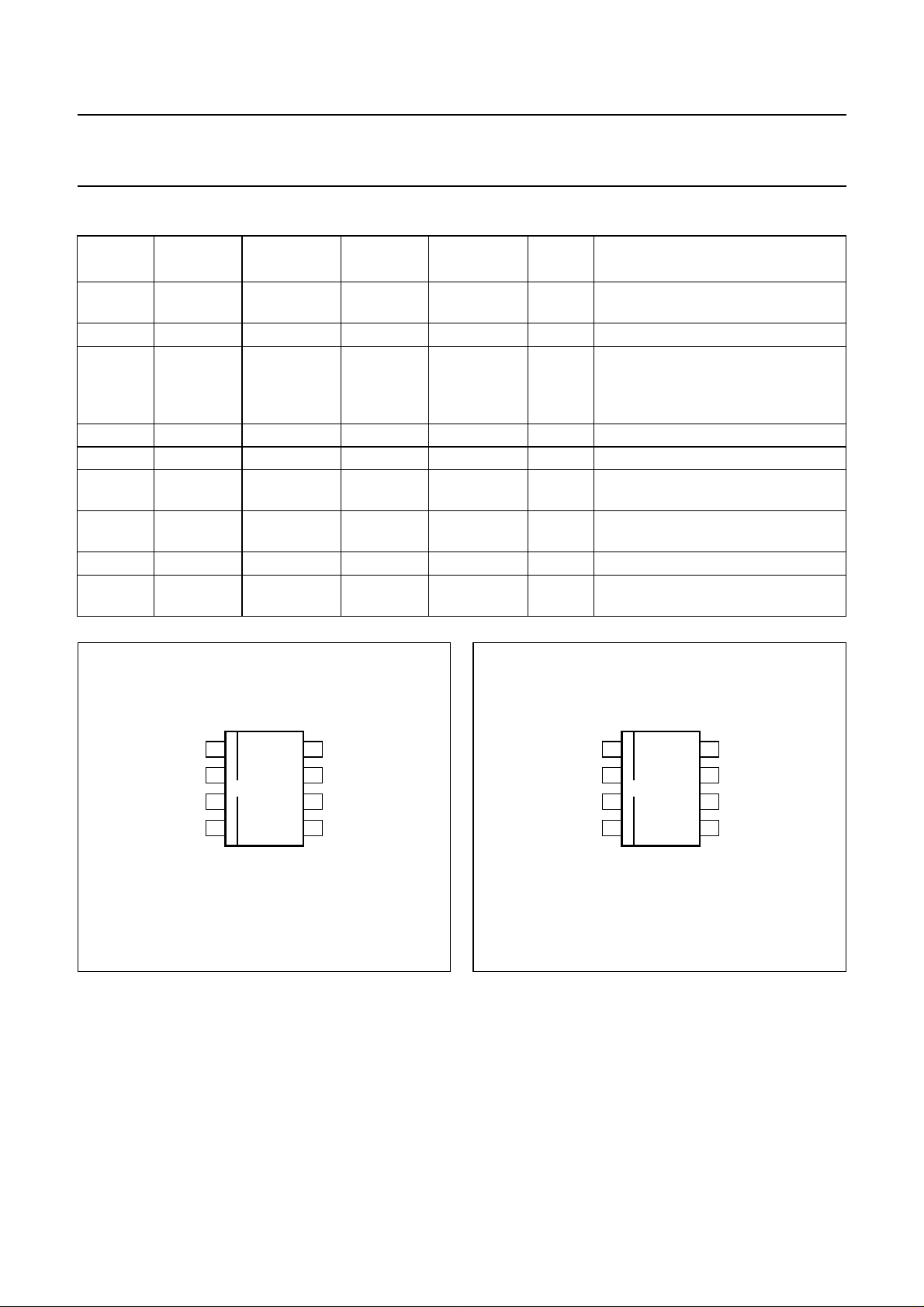
PINNING
SYMBOL
PIN
TZA3043T
DREF 1111analog
GND 2 2 2, 3 2, 3 ground ground
IPhoto 3344analog
GND 4 4 5, 6 5, 6 ground ground
GND 5 5 7, 8 7, 8 ground ground
OUT 6 7 9 10 data
OUTQ 7 6 10 9 data
V
CC
8 8 11, 12 11, 12 supply supply voltage
AGC −−13 13 input/
PIN
TZA3043BT
PAD
TZA3043U
PAD
TZA3043BU
TYPE DESCRIPTION
bias voltage for PIN diode; cathode
output
should be connected to this pin
current input; anode of PIN diode
input
should be connected to this pin;
DC bias levelof 822 mV is one diode
voltage above ground
data output; pin OUT goes HIGH
output
when current flows into pin IPhoto
compliment of pin OUT
output
AGC analog I/O
output
TZA3043; TZA3043B
handbook, halfpage
Fig.3 Pin configuration of TZA3043T.
DREF
IPhoto
GND
1
2
TZA3043T
3
4
MGR287
V
8
CC
OUTQGND
7
OUT
6
GND
5
handbook, halfpage
DREF
IPhoto
GND
1
2
TZA3043BT
3
4
MGU098
8
7
6
5
V
CC
OUTGND
OUTQ
GND
Fig.4 Pin configuration of TZA3043BT.
2000 Mar 28 4
Philips Semiconductors Product specification
Gigabit Ethernet/Fibre Channel
transimpedance amplifier
FUNCTIONAL DESCRIPTION
The TZA3043 is a transimpedance amplifier intended for
use in fibre optic links for signal recovery in Fibre Channel
or Gigabit Ethernet applications. It amplifies the current
generated by a photo detector (PIN diode or avalanche
photodiode) and transforms it into a differential output
voltage. The most important characteristics of the
TZA3043 are high receiver sensitivity and wide dynamic
range. High receiver sensitivity is achieved by minimizing
noise in the transimpedance amplifier.
Input circuit
The signal current generated by a PIN diode can vary
between 2.5 µA to 1.5 mA (p-p).
An AGC loop isimplemented tomake it possible to handle
such a wide dynamic range. The AGC loop increases the
dynamic range of the receiver by reducing the feedback
resistance of the preamplifier.
TZA3043; TZA3043B
The AGC loop hold capacitor is integrated on-chip, so an
external capacitor is not needed for AGC.
AGC monitoring
The AGC voltage can be monitored at pad 13 on the bare
die (TZA3043U/TZA3043BU). Pad 13 is not bonded in the
packaged device (TZA3043T/TZA3043BT). This pad can
beleftunconnected during normal operation.It canalsobe
used to force an external AGC voltage. If pad 13 (AGC) is
connected to GND, the internal AGC loop is disabled and
the receiver gain is at a maximum. The maximum input
current is then approximately 75 µA.
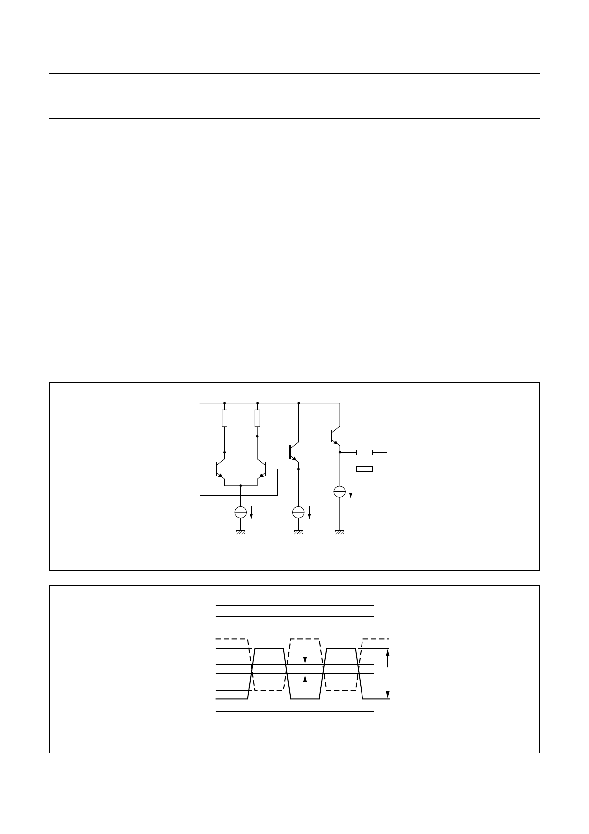
Output circuit
A differential amplifier converts the output of the
preamplifier to a differential voltage (see Fig.5).
The logic level symbol definitions for the differential
outputs are shown in Fig.6.
handbook, full pagewidth
handbook, full pagewidth
V
CC
V
O(max)
V
V
V
O(min)
800 Ω 800 Ω
2 mA
Fig.5 Differential data output circuit.
OQH
V
OH
OQL
V
OL
V
OO
4.5 mA
30 Ω
30 Ω
4.5 mA
MGR290
V
CC
V
o(p-p)
MGR243
OUTQ
OUT
Fig.6 Logic level symbol definitions for data outputs OUT and OUTQ.
2000 Mar 28 5
Philips Semiconductors Product specification
Gigabit Ethernet/Fibre Channel
transimpedance amplifier
PIN diode bias voltage DREF
The transimpedance amplifier together with the PIN diode
determines the performance of an optical receiver for a
large extent. Especiallyhow thePIN diode is connected to
the input and the layout around the input pin influence the
key parameters like sensitivity, the bandwidth and the
Power Supply Rejection Ratio (PSRR) of a
transimpedance amplifier. The total capacitance at the
inputpin is critical to obtainthehighest sensitivity. It should
be kept to a minimum by reducing the capacitance of the
PIN diode and the parasitics around the input pin. The
PIN diode should be placed very close to the IC to reduce
the parasitics. Because the capacitance of the PIN diode
depends on the reverse voltage across it, the reverse
voltage should be chosen as high as possible.
The PIN diode can be connected to the input in two ways
as shown in Figs 7 and 8. In Fig.7 the PIN diode is
connected between pins DREF and IPhoto. Pin DREF
provides an easy bias voltage for the PIN diode. The
voltage at DREF is derived from VCC by a low-pass filter.
The low-pass filter consisting of the internal resistors
R1, R2, C1 and the external capacitor C2 rejects the
supply voltage noise.The external capacitor C2 should be
equal or larger then 1 nF for a high PSRR.
TZA3043; TZA3043B
The reverse voltage across the PIN diode is 4.18 V
(5 − 0.82 V) for 5 V supply or 2.48 V (3.3 − 0.82 V) for
3.3 V supply.
It is preferable to connect the cathode of the PIN diode to
a higher voltage then VCC when such a voltage source is
available on the board. In this case pin DREF can be left
unconnected.Whenanegativesupply voltage is available,
the configuration in Fig.8 can be used. It should be noted
that in this case the direction of the signal current is
reversed compared tothe Fig.7. Properfiltering of the bias
voltage for the PIN diode is essential to achieve the
highest sensitivity level.
V
CC
8
R1
125 Ω
C1
10 pF
MGU103
C2
1 nF
I
i
DREF
IPhoto
R2
125 Ω
1
3
TZA3043
Fig.7 ThePIN diodeconnectedbetweentheinput
and pin DREF.
2000 Mar 28 6
V
CC
8
R1
125 Ω
C1
10 pF
MGU104
1
DREF
IPhoto
3
I
i
negative supply voltage
R2
125 Ω
TZA3043
Fig.8 ThePIN diodeconnectedbetweentheinput
and a negative supply voltage.
Philips Semiconductors Product specification
Gigabit Ethernet/Fibre Channel
transimpedance amplifier
AGC
The TZA3043 transimpedance amplifier can handle input
currents from 1 µA to 1.5 mA. This means a dynamic
range of 63 dB. At low input currents, the transimpedance
must be high to get enough output voltage, and the noise
should be low enough to guaranty minimum bit error rate.
At high input currents however, the transimpedance
should be low to avoid pulse width distortion. This means
that the gain of the amplifier has to vary depending on the
input signal level to handle such a wide dynamic range.
This is achieved in the TZA3043 by implementing an
Automatic Gain Control (AGC) loop. The AGC loop
consists of a peak detector, a hold capacitor and a gain
control circuit.
The peak amplitude of the signal is detected by the peak
detector and it is stored on the holdcapacitor. The voltage
over the hold capacitor is compared to a threshold level.
Thethreshold level is setto25 µA (p-p)input current. AGC
becomes active only for input signals larger than the
threshold level.
TZA3043; TZA3043B
It is disabled for smaller signals. The transimpedance is
then at its maximum value (8.3 kΩ differential).
When AGC is active, the feedback resistor of the
transimpedance amplifier is reduced to keep the output
voltage constant. The transimpedance is regulated from
8.3 kΩ at low currents (I < 30 µA) to 1 kΩ at high currents
(I < 500 µA). Above 500 µA the transimpedance is at its
minimum and can not be reduced further but the front-end
remains linear until input currents of 1.5 mA.
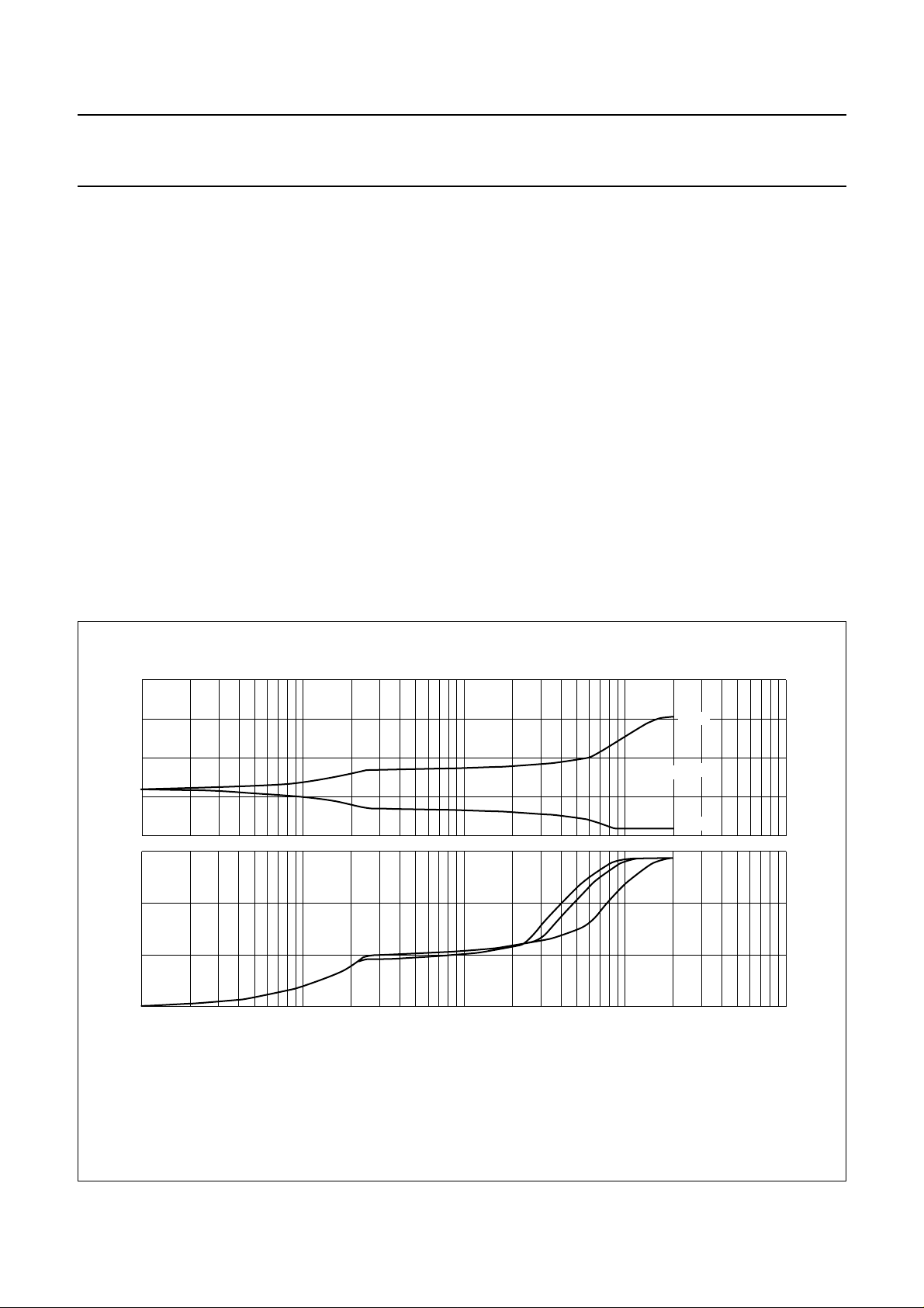
The upper part of Fig.9 shows the output voltages of the
TZA3043 (OUT and OUTQ) as a function of the DC input
current. In the lower part, the difference of both voltages is
shown. It can be seen from the figure that the output
changes linearly up to 25 µA input current where AGC
becomes active. From this point on, AGC tries to keep the
differential output voltage constant around 200 mV for
medium range input currents (input currents <200 µA).
The AGC can not regulate any more above 500 µA input
current and the output voltage rises again with the input
current.
3.9
handbook, full pagewidth
V
o
(V)
3.7
3.5
3.3
3.1
600
V
o(dif)
(mV)
400
200
0
110
V
o(dif)=VOUT
(1) VCC=3V.
(2) VCC= 3.3 V.
(3) VCC=5V.
− V
OUTQ
MGU105
V
OUT
VCC = 5 V
V
OUTQ
(1)
(2)
(3)
10
.
2
3
10
Ii (µA)
4
10
Fig.9 AGC characteristics.
2000 Mar 28 7
Philips Semiconductors Product specification
Gigabit Ethernet/Fibre Channel
TZA3043; TZA3043B
transimpedance amplifier
LIMITING VALUES
In accordance with the Absolute Maximum Rating System (IEC 60134).
SYMBOL PARAMETER MIN. MAX. UNIT
V
CC
V
n
I
n
P
tot
T
stg
T
j
T
amb
supply voltage −0.5 +6 V
DC voltage
pin/pad IPhoto −0.5 +1 V
pins/pads OUT and OUTQ −0.5 V
pad AGC (bare die only) −0.5 V
pin/pad DREF −0.5 V
+ 0.5 V
CC
+ 0.5 V
CC
+ 0.5 V
CC
DC current
pin/pad IPhoto −2.5 +2.5 mA
pins/pads OUT and OUTQ −15 +15 mA
pad AGC (bare die only) −0.2 +0.2 mA
pin/pad DREF −2.5 +2.5 mA
total power dissipation − 300 mW
storage temperature −65 +150 °C
junction temperature − 150 °C
ambient temperature −40 +85 °C
HANDLING
Precautions should be taken to avoid damage through electrostatic discharge. This is particularly important during
assembly and handling of the bare die. Additional safety can be obtained by bonding the VCC and GND pads first, the
remaining pads may then be bonded to their external connections in any order.
THERMAL CHARACTERISTICS
SYMBOL PARAMETER VALUE UNIT
R
th(j-a)
thermal resistance from junction to ambient 160 K/W
2000 Mar 28 8
Philips Semiconductors Product specification
Gigabit Ethernet/Fibre Channel
TZA3043; TZA3043B
transimpedance amplifier
CHARACTERISTICS
Typical values at T
temperature range and supply range; all voltages are measured with respect to ground; unless otherwise specified.
SYMBOL PARAMETER CONDITIONS MIN. TYP. MAX. UNIT
V
CC
I
CC
P
tot
T
j
T
amb
R
tr
supply voltage 3 5 5.5 V
supply current AC coupled; RL=50Ω− 34 47 mA
total power dissipation VCC=5V − 170 259 mW
junction temperature −40 − +125 °C
ambient temperature −40 +25 +85 °C
small-signal transresistance of
the receiver
f
−3dB(h)
high frequency −3 dB point VCC=5V; Ci= 0.7 pF 1000 1200 − MHz
PSRR power supply rejection ratio measured differentially;
Bias voltage: pin DREF
R
DREF
resistance between DREF and
V
Input: pin IPhoto
V
bias(IPhoto)
input bias voltage on
pin IPhoto
I
i(IPhoto)(p-p)
input current on pin IPhoto
(peak-to-peak value)
R
i
I
n(tot)
small-signal input resistance fi= 1 MHz; input current
total integrated RMS noise
current over bandwidth
=25°C and VCC= 5 V; minimum and maximum values are valid over the entire ambient
amb
V
= 3.3 V − 112 169 mW
CC
measured differentially;
AC coupled
R
= ∞ 13.2 16.6 20 kΩ
L
R
=50Ω 6.6 8.3 10 kΩ
L
V
= 3.3 V; Ci= 0.7 pF 850 1100 − MHz
CC
note 1
f = 1 to 100 MHz − 2 −µA/V
f = 1 GHz − 66 −µA/V
tested at DC 210 250 290 Ω
CC
600 822 1000 mV
VCC= 5 V; note 2 −1500 +6 +1500 µA
V
= 3.3 V; note 2 −1000 +6 +1000 µA
CC
− 28 −Ω
<2 µA (p-p)
referenced to input;
− 200 − nA
∆f = 920 MHz; note 3
2000 Mar 28 9
 Loading...