

Philips TZA3041U, TZA3041BHL, TZA3041AHL Datasheet

INTEGRATED CIRCUITS
DATA SH EET
TZA3041AHL; TZA3041BHL;
TZA3041U
Gigabit Ethernet/Fibre Channel
laser drivers
Preliminary specification
Supersedes data of 1998 Aug 24
File under Integrated Circuits, IC19
1999 Aug 24

Philips Semiconductors Preliminary specification
Gigabit Ethernet/Fibre Channel
laser drivers
FEATURES
• 1.2 Gbits/s data input, both Current-Mode Logic (CML)
and PositiveEmitter Coupled Logic (PECL) compatible;
maximum 800 mV (p-p)
• Adaptive laser output control with dual loop, stabilizing
optical ONE and ZERO levels
• Optionalexternalcontroloflasermodulationandbiasing
currents (non-adaptive)
• Automatic laser shutdown
• Few external components required
• Rise and fall times of 120 ps (typical value)
• Jitter <50 mUI (p-p)
• RF output current sinking capability of 60 mA
• Bias current sinking capability of 90 mA
• Power dissipation of 430 mW (typical value)
• Low cost LQFP32 plastic package
• Single 5 V power supply.
TZA3041AHL; TZA3041BHL;
TZA3041U
APPLICATIONS
• Gigabit Ethernet/Fibre Channel optical transmission
systems
• Gigabit Ethernet/Fibre Channel optical laser modules.
GENERAL DESCRIPTION
The TZA3041AHL, TZA3041BHL and TZA3041U are fully
integrated laser drivers for Gigabit Ethernet/Fibre Channel
(1.2 Gbits/s) systems, incorporating the RF path between
the data multiplexer and the laser diode. Since the dual
loop bias and modulation control circuits are integrated on
the IC, the external component count is low. Only
decoupling capacitors and adjustment resistors are
required.
TheTZA3041AHL features an alarm function for signalling
extreme bias current conditions. The alarm low and high
threshold levels can be adjusted to suit the application
using only a resistor or a current Digital-to-Analog
Converter (DAC).
TZA3041AHL
• Laser alarm output for signalling extremely low and high
bias current conditions.
TZA3041BHL
• Extra 1.2 Gbits/s loop mode input; both CML and PECL
compatible.
TZA3041U
• Bare die version with combined bias alarm and loop
mode functionality.
ORDERING INFORMATION
TYPE
NUMBER
TZA3041AHL LQFP32 plastic low profile quad flat package; 32 leads; body 5 × 5 × 1.4 mm SOT401-1
TZA3041BHL
TZA3041U − bare die; 2000 × 2000 × 380 µm −
NAME DESCRIPTION VERSION
The TZA3041BHL is provided with an additional RF data
input to facilitate remote (loop mode) system testing.
The TZA3041U is a bare die version for use in compact
laser module designs. The die contains 40 pads and
features the combined functionality of the TZA3041AHL
and the TZA3041BHL.
PACKAGE
1999 Aug 24 2
Philips Semiconductors Preliminary specification
Gigabit Ethernet/Fibre Channel
laser drivers
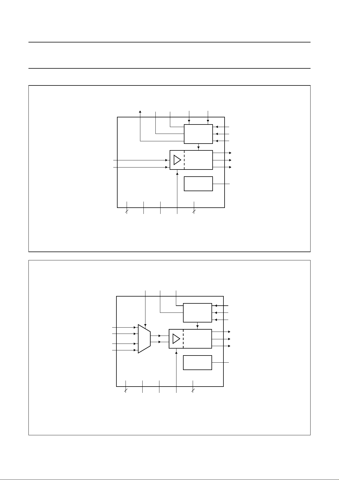
BLOCK DIAGRAMS
handbook, full pagewidth
28
DIN
DINQ
29
V
CC(R)
19, 20
27, 30
TZA3041AHL; TZA3041BHL;
ALARM
26
data input
(differential)
TONE
4
ALARMLO
TZA3041AHL
31
10
7
411
V
CC(G)
V
CC(B)
ALS
ALARMHITZERO
215
LASER
CONTROL
BLOCK
CURRENT
SWITCH
BAND GAP
REFERENCE
1, 3, 8, 9,
11, 14, 16, 17
24, 25, 32
GND
18
MBK874
2
MONIN
22
ONE
23
ZERO
13
LA
12
LAQ
15
BIAS
6
BGAP
TZA3041U
handbook, full pagewidth
DIN
DINQ
DLOOP
DLOOPQ
Fig.1 Block diagram of TZA3041AHL.
TONE
10
CC(B)
4
TZERO
31
ALS
LASER
CONTROL
BLOCK
CURRENT
SWITCH
BAND GAP
REFERENCE
1, 3, 8, 9,
11, 14, 16, 17
24, 25, 32
GND
22
23
13
12
15
MBK873
2
MONIN
ONE
ZERO
LA
LAQ
BIAS
6
BGAP
ENL
26 5
28
29
19
20
MUX
TZA3041BHL
18, 21
7
27, 30
411
V
V
V
CC(R)
CC(G)
Fig.2 Block diagram of TZA3041BHL.
1999 Aug 24 3

Philips Semiconductors Preliminary specification
Gigabit Ethernet/Fibre Channel
laser drivers
TZA3041AHL; TZA3041BHL;
TZA3041U
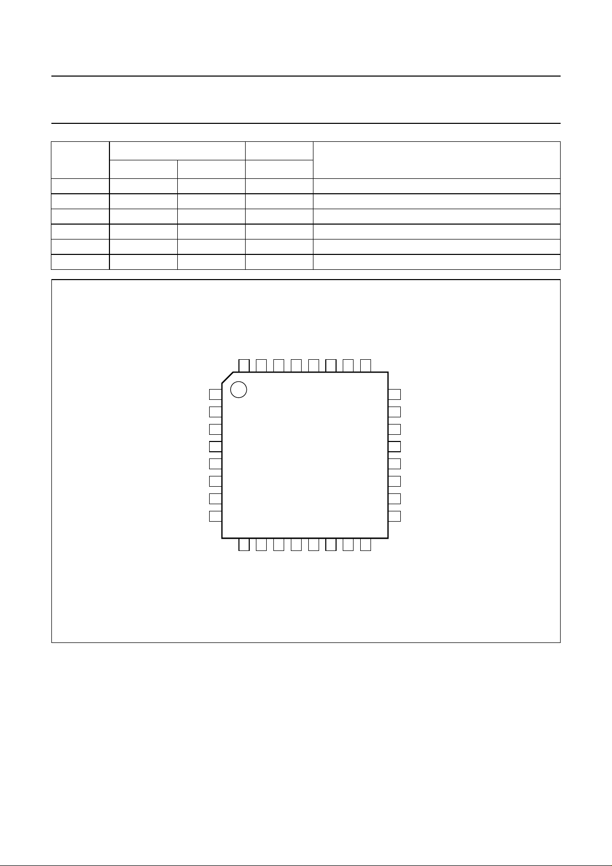
PINNING
PIN PAD
SYMBOL
DESCRIPTION
TZA3041AHL TZA3041BHL TZA3041U
GND 1 1 1 ground
MONIN 2 2 2 monitor photodiode current input
GND 3 3 3 ground
IGM −−4 not used; leave unbonded
TONE 4 4 5 connection for external capacitor used to set optical
ONE control loop time constant (optional)
TZERO 5 5 6 connection for external capacitor used to set optical
ZERO control loop time constant (optional)
BGAP 6 6 7 connection for external band gap decoupling capacitor
V
CC(G)
V
CC(G)
7 7 8 supply voltage (green domain)
−−9 supply voltage (green domain)
GND 8 8 10 ground
GND 9 9 11 ground
V
V
CC(B)
CC(B)
10 10 12 supply voltage (blue domain)
−−13 supply voltage (blue domain)
GND 11 11 14 ground
LAQ 12 12 15 laser modulation output inverted
LA 13 13 16 laser modulation output
GND 14 14 17 ground
BIAS 15 15 18 laser bias current output
GND 16 16 19 ground
GND 17 17 20 ground
GND −−21 ground
ALARMHI 18 − 22 maximum bias current alarm reference level input
V
CC(R)
V
CC(R)
− 18 23 supply voltage (red domain)
19 −−supply voltage (red domain)
DLOOP − 19 24 loop mode data input
V
CC(R)
20 −−supply voltage (red domain)
DLOOPQ − 20 25 loop mode data input inverted
V
CC(R)
−−26 supply voltage (red domain)
ALARMLO 21 − 27 minimum bias current alarm reference level input
V
CC(R)
− 21 − supply voltage (red domain)
ONE 22 22 28 optical ONE reference level input
ZERO 23 23 29 optical ZERO reference level input
GND 24 24 30 ground
GND 25 25 31 ground
ALARM 26 − 32 alarm output
ENL − 26 33 loop mode enable input
V
CC(R)
27 27 34 supply voltage (red domain)
1999 Aug 24 4
Philips Semiconductors Preliminary specification
Gigabit Ethernet/Fibre Channel
TZA3041AHL; TZA3041BHL;
laser drivers
SYMBOL
TZA3041AHL TZA3041BHL TZA3041U
DIN 28 28 35 data input
DINQ 29 29 36 data input inverted
V
CC(R)
30 30 37 supply voltage (red domain)
ALS 31 31 38 automatic laser shutdown input
GND 32 32 39 ground
GND −−40 ground
handbook, full pagewidth
PIN PAD
ALS
GND
31
32
CC(R)
V
30
DINQ
29
DIN
28
CC(R)
V
27
ALARM
26
DESCRIPTION
GND
25
TZA3041U
GND
MONIN
GND
TONE
TZERO
BGAP
V
CC(G)
GND
1
2
3
4
5
6
7
8
9
GND
TZA3041AHL
11
10
GND
CC(B)
V
12
LAQ
LA
13
14
15
16
GND
BIAS
GND
Fig.3 Pin configuration of TZA3041AHL.
24
23
22
21
20
19
18
17
MBK870
GND
ZERO
ONE
ALARMLO
V
CC(R)
V
CC(R)
ALARMHI
GND
1999 Aug 24 5
Philips Semiconductors Preliminary specification
Gigabit Ethernet/Fibre Channel
laser drivers
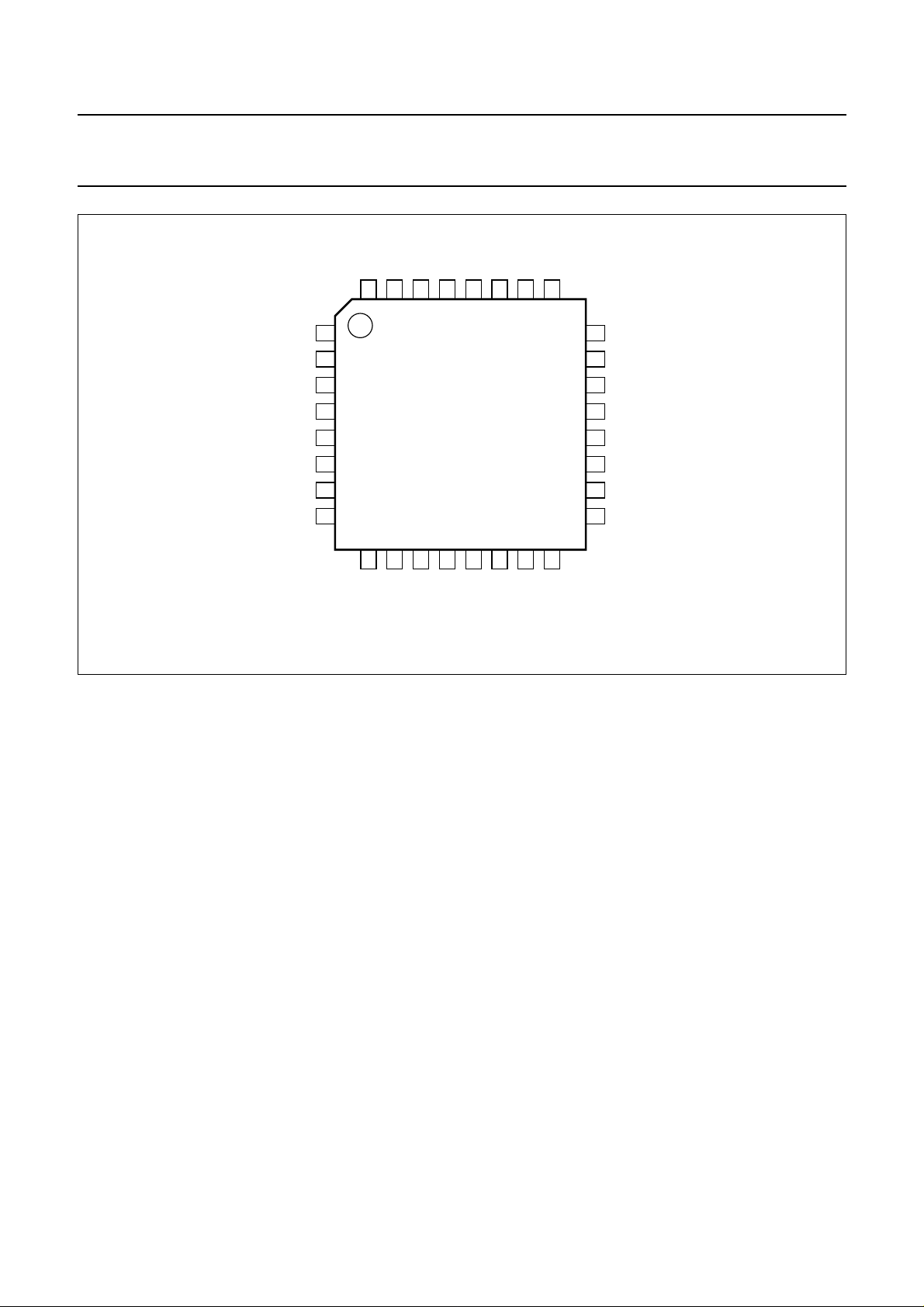
handbook, full pagewidth
1
GND
GND
TONE
BGAP
CC(G)
GND
2
3
4
5
6
7
8
MONIN
TZERO
V
GND
32
9
GND
CC(R)
ALS
V
31
30
TZA3041BHL
11
10
GND
CC(B)
V
DINQ
29
12
LAQ
DIN
28
13
LA
TZA3041AHL; TZA3041BHL;
TZA3041U
CC(R)
ENL
V
27
14
GND
26
15
BIAS
GND
25
16
GND
24
23
22
21
20
19
18
17
MBK875
GND
ZERO
ONE
V
CC(R)
DLOOPQ
DLOOP
V
CC(R)
GND
Fig.4 Pin configuration of TZA3041BHL.
FUNCTIONAL DESCRIPTION
The TZA3041AHL, TZA3041BHL and TZA3041U laser
drivers accept a 1.2 Gbits/s Non-Return to Zero (NRZ)
input data stream and generate an output signal with
sufficient current to drive a solid state Fabry Perot (FP) or
Distributed FeedBack (DFB) laser. They also contain dual
loop control circuitry for stabilizing the true laser optical
power levels representing logic 1 and logic 0.
The input buffers present a high impedance to the data
stream on the differential inputs (pins DIN and DINQ).
The input signal can be at CML level of approximately
200 mV (p-p) below the supply voltage, or at PECL level
upto 800 mV (p-p). The inputs can beconfiguredtoaccept
CML signals by connecting external 50 Ω pull-up resistors
between pins DIN and DINQ to V
CC(R)
. If PECL
compatibility is required, the usual Thevenin termination
can be applied.
For ECL signals (negative and referenced to ground) the
inputs should be AC-coupled to the signal source.
If AC-coupling is applied, a constant input signal (either
low of high) will bring the device in an undefined state.
To avoid this, it is recommended to apply a slight offset to
the input stage. The applied offset must be higher than the
specified value in Chapter “Characteristics”, but much
lower than the applied input voltage swing.
The RF path is fully differential and contains a differential
preamplifier and a main amplifier. The main amplifier is
designed to handle large peak currents required at the
output laser driving stage and is insensitive to supply
voltage variations. The output signal from the main
amplifier drives a current switch which supplies a
guaranteed maximum modulation current of 60 mA at
pins LA and LAQ. Pin BIAS delivers a guaranteed
maximum DC bias current of up to 90 mA for adjusting the
optical laser output to a level above its light emitting
threshold.
Automatic laser control
A laser with a Monitor PhotoDiode (MPD) is required for
the laser control circuit (see Figs 6 and 7).
The MPD current is proportional to the laser emission and
is applied to pin MONIN. The MPD current range is from
100 to 1000 µA (p-p). The inputbufferisoptimized to cope
with MPD capacitances up to 50 pF. To prevent the input
buffer breaking into oscillation with a low MPD
capacitance, it is required to increase the capacitance to
the minimum value specified in Chapter “Characteristics”
by connecting an extra capacitor between pin MONIN and
V
.
CC(G)
1999 Aug 24 6

Philips Semiconductors Preliminary specification
Gigabit Ethernet/Fibre Channel
laser drivers
DC reference currents are applied to pins ZERO and ONE
to set the MPD reference levels for laser LOW and laser
HIGH.A resistor connected between pin ZERO and V
and a resistor connected between pin ONE and V
sufficient, but current DACs can also be used.
The voltages on pins ZERO and ONE are held constant at
a level of 1.5 V below V
. The reference current
CC(R)
applied to pin ZERO is multiplied by 4 and the reference
current flowing into pin ONE is multiplied internally by 16.
The reference current and the resistor for the optical ONE
regulation loop (modulation current control) can be
calculated using the following formulae:
I
ONE
R
1
×= A[]
I
------
MPD (ONE)
16
1.5
== Ω[]
ONE
----------I
ONE
24
------------------------I
MPD (ONE)
The reference current and resistor for the optical ZERO
regulation loop (bias current control) can be calculated
using the following formulae:
1
×= A[]
I
ZERO
I
-- 4
MPD (ZERO)
CC(R)
CC(R)
is
(1)
(2)
(3)
TZA3041AHL; TZA3041BHL;
TZA3041U
Itshouldbenoted that the MPD current is stabilized, rather
than the actual laser optical output power. Deviations
between optical output power and MPD current, known as
‘tracking errors’, cannot be corrected.
Designing the modulation and bias loop
TheopticalONE and ZERO regulation loop time constants
are determined by on-chip capacitances. If the resulting
time constants are found to be too small in a specific
application, they can be increased by connecting external
capacitors to pins TZERO and TONE, respectively.
The optical ONE loop time constant and bandwidth can be
estimated using the following formulae:
3
×
80 10
×= s[]
----------------------
η
LASER
LASER
+()× 80× 103×
TONE
(5)
(6)
B
B
τ
ONE
ONE
ONE
40 10
1
= Hz[]
------------------------- 2πτ
×
ONE
=
------------------------------------------------------------------------------------------------2π 40 10
12–
C
+×()
TONE
η
12–
× C
R
ZERO
1.5
== Ω[]
-------------I
ZERO
In these formulae, I
6
---------------------------I
MPD (ZERO)
MPD(ONE)
and I
MPD(ZERO)
(4)
represent the
monitor photodiode current during an optical ONE and an
optical ZERO, respectively.
Example: A laser is operating at optical output power
levels of 0.3 mW for laser HIGH and 0.03 mW for laser
LOW (extinction ratio of 10 dB). Suppose the
corresponding MPD currents for this type of laser are
260 and 30 µA, respectively.
In this example the reference current is
I
ONE
1
260× 16.25 µA==
-----16
and flows into pin ONE.
This current can be set using a current source or simply by
a resistor of the appropriate value connected between
pin ONE and V
R
ONE
1.5
----------------
16.25
. In this example the resistor would be
CC(R)
92.3 kΩ==
The reference current at pin ZERO in this example is
I
ZERO
R
ZERO
1
30× 7.5˙µA==
-- 4
1.5
--------- -
7.5
and can be set using a resistor
200 kΩ==
The optical ZERO loop time constant and bandwidth can
be estimated using the following formulae:
τ
ZERO
B
B
= Hz[]
ZERO
=
ZERO
The term η
40 10
---------------------------2πτ
---------------------------------------------------------------------------------------------------2π 40 10
LASER
12–
C
+×()
TZERO
1
×
ZERO
η
LASER
12–
+×()× 50× 103×
(dimensionless) in the above formulae is
50 10
×= s[]
----------------------
C
TZERO
η
LASER
3
×
the product of the two terms:
•ηEO is the electro-optical efficiency which accounts for
the steepness of the laser slope. It is the amount of the
extra optical output power in W/A of modulation current
optical output power.
• R is the monitor photodiode responsivity. It is the
amount of the extra monitor photodiode current in A/W
optical output power.
(7)
(8)
1999 Aug 24 7
 Loading...