

Philips TZA3041U, TZA3041BHL, TZA3041AHL Datasheet

INTEGRATED CIRCUITS
DATA SH EET
TZA3041AHL; TZA3041BHL;
TZA3041U
Gigabit Ethernet/Fibre Channel
laser drivers
Product specification
Supersedes data of 1999 Aug 24
File under Integrated Circuits, IC19
2000 Feb 22

Philips Semiconductors Product specification
Gigabit Ethernet/Fibre Channel laser
drivers
FEATURES
• 1.2 Gbits/s data input, both Current Mode Logic (CML)
and PositiveEmitter Coupled Logic (PECL) compatible;
maximum 800 mV (p-p)
• Adaptive laser output control with dual loop, stabilizing
optical 1 and 0 levels
• Optionalexternalcontroloflasermodulationandbiasing
currents (non-adaptive)
• Automatic laser shutdown
• Few external components required
• Rise and fall times of 120 ps (typical value)
• Jitter <50 mUI (p-p)
• RF output current sinking capability of 60 mA
• Bias current sinking capability of 90 mA
• Power dissipation of 430 mW (typical value)
• Low cost LQFP32 5 × 5 plastic package
• Single 5 V power supply.
TZA3041AHL; TZA3041BHL;
TZA3041U
APPLICATIONS
• Gigabit Ethernet/Fibre Channel optical transmission
systems
• Gigabit Ethernet/Fibre Channel optical laser modules.
GENERAL DESCRIPTION
The TZA3041AHL, TZA3041BHL and TZA3041U are fully
integrated laser drivers for Gigabit Ethernet/Fibre Channel
(1.2 Gbits/s) systems, incorporating the RF path between
the data multiplexer and the laser diode. Since the dual
loop bias and modulation control circuits are integrated on
the IC, the external component count is low. Only
decoupling capacitors and adjustment resistors are
required.
TheTZA3041AHL features an alarm function for signalling
extreme bias current conditions. The alarm low and high
threshold levels can be adjusted to suit the application
using only a resistor or a current Digital-to-Analog
Converter (DAC).
TZA3041AHL
• Laser alarm output for signalling extremely low and high
bias current conditions.
TZA3041BHL
• Extra 1.2 Gbits/s loop mode input; both CML and PECL
compatible.
TZA3041U
• Bare die version with combined bias alarm and loop
mode functionality.
ORDERING INFORMATION
TYPE
NUMBER
TZA3041AHL LQFP32 plastic low profile quad flat package; 32 leads; body 5 × 5 × 1.4 mm SOT401-1
TZA3041BHL
TZA3041U − bare die; 2000 × 2000 × 380 µm −
NAME DESCRIPTION VERSION
The TZA3041BHL is provided with an additional RF data
input to allow remote system testing (loop mode).
The TZA3041U is a bare die version for use in compact
laser module designs. The die contains 40 pads and
features the combined functionality of the TZA3041AHL
and the TZA3041BHL.
PACKAGE
2000 Feb 22 2
Philips Semiconductors Product specification
Gigabit Ethernet/Fibre Channel laser
drivers
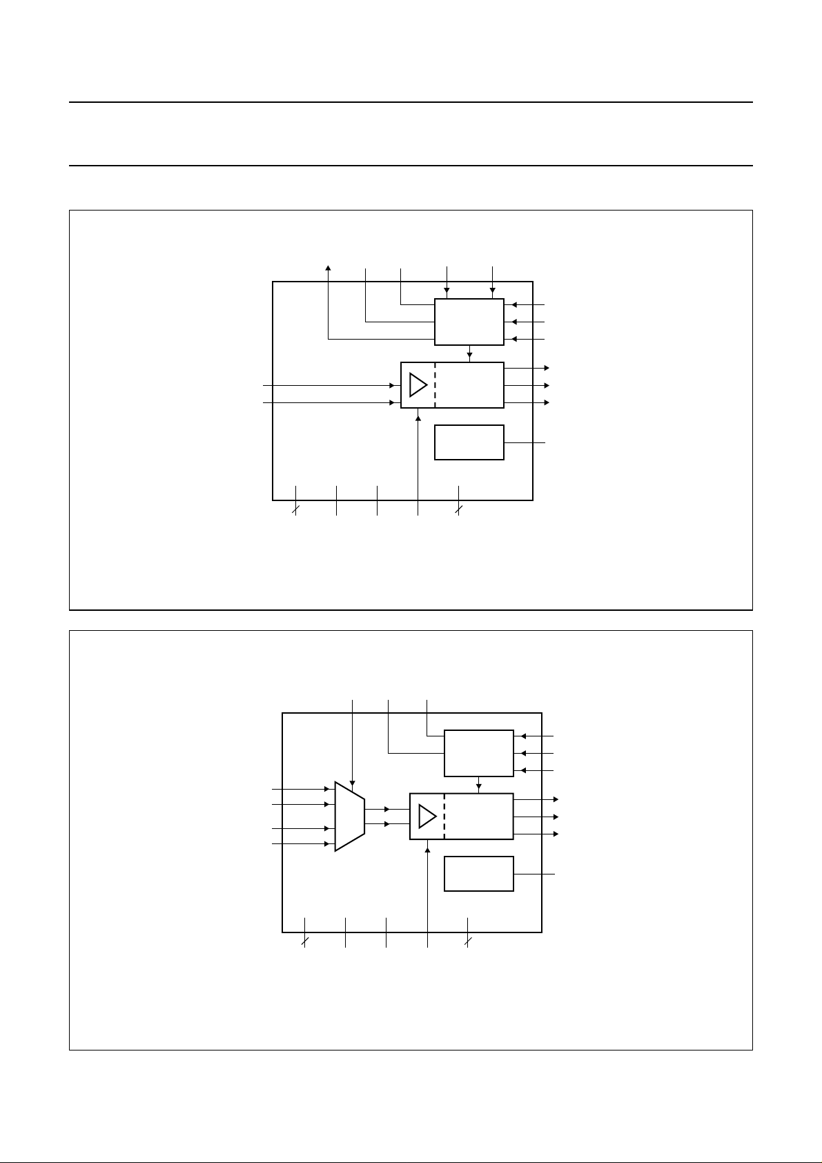
BLOCK DIAGRAM
TONE
handbook, full pagewidth
DIN
DINQ
ALARM
26
data input
(differential)
28
29
TZA3041AHL
19, 20
7
27, 30
411
V
CC(R)
V
CC(G)
V
4
10
CC(B)
ALARMLO
31
ALS
TZA3041AHL; TZA3041BHL;
ALARMHITZERO
215
LASER
CONTROL
BLOCK
CURRENT
SWITCH
BAND GAP
REFERENCE
1, 3, 8, 9,
11, 14, 16, 17
24, 25, 32
GND
18
MBK874
TZA3041U
2
MONIN
22
ONE
23
ZERO
13
LA
12
LAQ
15
BIAS
6
BGAP
handbook, full pagewidth
DIN
DINQ
DLOOP
DLOOPQ
Fig.1 Block diagram of TZA3041AHL.
TONE
10
CC(B)
4
TZERO
31
ALS
LASER
CONTROL
BLOCK
CURRENT
SWITCH
BAND GAP
REFERENCE
1, 3, 8, 9,
11, 14, 16, 17
24, 25, 32
GND
22
23
13
12
15
MBK873
2
MONIN
ONE
ZERO
LA
LAQ
BIAS
6
BGAP
ENL
26 5
28
29
19
20
MUX
TZA3041BHL
18, 21
7
27, 30
411
V
CC(R)
V
CC(G)
V
Fig.2 Block diagram of TZA3041BHL.
2000 Feb 22 3

Philips Semiconductors Product specification
Gigabit Ethernet/Fibre Channel laser
drivers
TZA3041AHL; TZA3041BHL;
TZA3041U
PINNING
PIN PAD
SYMBOL
DESCRIPTION
TZA3041AHL TZA3041BHL TZA3041U
GND 1 1 1 ground
MONIN 2 2 2 monitor photodiode current input
GND 3 3 3 ground
IGM −−4 not connected
TONE 4 4 5 connection for external capacitor used for setting
optical 1 control loop time constant (optional)
TZERO 5 5 6 connection for external capacitor used for setting
optical 0 control loop time constant (optional)
BGAP 6 6 7 connection for external band gap decoupling
capacitor
V
CC(G)
V
CC(G)
7 7 8 supply voltage (green domain); note 1
−−9 supply voltage (green domain); note 1
GND 8 8 10 ground
GND 9 9 11 ground
V
V
CC(B)
CC(B)
10 10 12 supply voltage (blue domain); note 2
−−13 supply voltage (blue domain); note 2
GND 11 11 14 ground
LAQ 12 12 15 laser modulation output inverted
LA 13 13 16 laser modulation output
GND 14 14 17 ground
BIAS 15 15 18 laser bias current output
GND 16 16 19 ground
GND 17 17 20 ground
GND −−21 ground
ALARMHI 18 − 22 maximum bias current alarm reference level input
V
CC(R)
V
CC(R)
− 18 23 supply voltage (red domain); note 3
19 −−supply voltage (red domain); note 3
DLOOP − 19 24 loop mode data input
V
CC(R)
20 −−supply voltage (red domain); note 3
DLOOPQ − 20 25 loop mode data input inverted
V
CC(R)
−−26 supply voltage (red domain); note 3
ALARMLO 21 − 27 minimum bias current alarm reference level input
V
CC(R)
− 21 − supply voltage (red domain); note 3
ONE 22 22 28 optical 1 reference level input
ZERO 23 23 29 optical 0 reference level input
GND 24 24 30 ground
GND 25 25 31 ground
ALARM 26 − 32 alarm output
ENL − 26 33 loop mode enable input
2000 Feb 22 4
Philips Semiconductors Product specification
Gigabit Ethernet/Fibre Channel laser
drivers
TZA3041AHL; TZA3041BHL;
TZA3041U
PIN PAD
SYMBOL
DESCRIPTION
TZA3041AHL TZA3041BHL TZA3041U
V
CC(R)
27 27 34 supply voltage (red domain); note 3
DIN 28 28 35 data input
DINQ 29 29 36 data input inverted
V
CC(R)
30 30 37 supply voltage (red domain); note 3
ALS 31 31 38 automatic laser shutdown input
GND 32 32 39 ground
GND −−40 ground
Notes
1. Supply voltage for the Monitor PhotoDiode (MPD) input current.
2. Supply voltage for the laser modulation outputs (LA, LAQ).
3. Supply voltage for the data inputs (DIN, DINQ), optical 1 and 0 reference level inputs (ONE, ZERO), and the bias
current alarm reference level inputs (ALARMHI, ALARMLO).
handbook, full pagewidth
GND
MONIN
GND
TONE
TZERO
BGAP
V
CC(G)
GND
CC(R)
ALS
GND
32
1
2
3
4
5
6
7
8
9
GND
V
31
30
TZA3041AHL
11
10
GND
CC(B)
V
DINQ
29
12
LAQ
DIN
28
13
LA
CC(R)
V
27
14
GND
ALARM
26
15
BIAS
GND
25
16
GND
Fig.3 Pin configuration of TZA3041AHL.
24
23
22
21
20
19
18
17
MBK870
GND
ZERO
ONE
ALARMLO
V
CC(R)
V
CC(R)
ALARMHI
GND
2000 Feb 22 5
Philips Semiconductors Product specification
Gigabit Ethernet/Fibre Channel laser
drivers
handbook, full pagewidth
ALS
GND
31
32
1
GND
GND
TONE
BGAP
CC(G)
GND
2
3
4
5
6
7
8
9
10
GND
CC(B)
V
MONIN
TZERO
V
CC(R)
V
30
DINQ
29
DIN
28
TZA3041BHL
11
12
13
LA
LAQ
GND
TZA3041AHL; TZA3041BHL;
TZA3041U
CC(R)
ENL
V
27
14
GND
26
15
BIAS
GND
25
16
GND
24
23
22
21
20
19
18
17
MBK875
GND
ZERO
ONE
V
CC(R)
DLOOPQ
DLOOP
V
CC(R)
GND
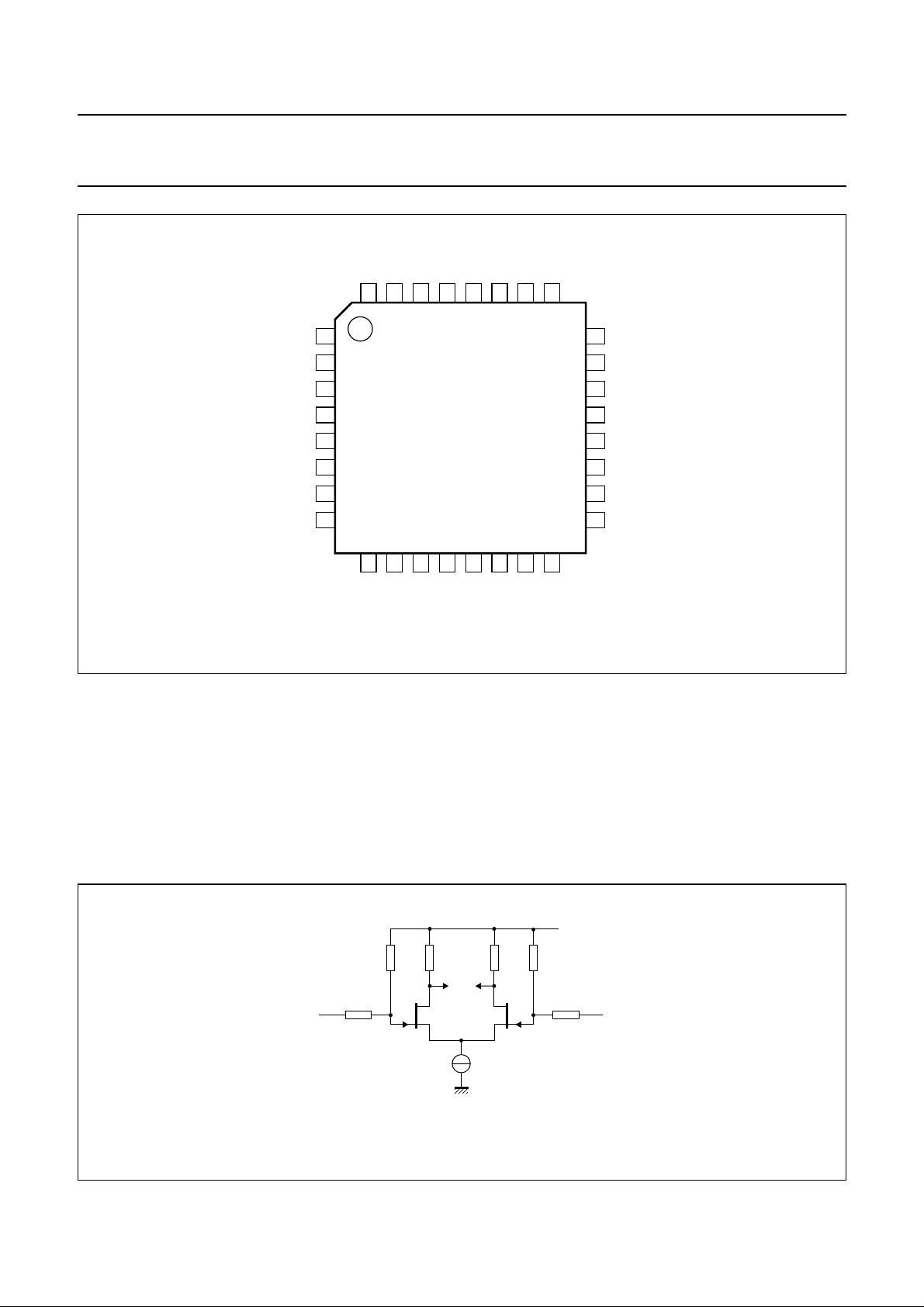
Fig.4 Pin configuration of TZA3041BHL.
FUNCTIONAL DESCRIPTION
The TZA3041AHL, TZA3041BHL and TZA3041U laser
drivers accept a 1.2 Gbits/s Non-Return to Zero (NRZ)
input data stream, and generate an output signal with
sufficient current to drive a solid state Fabry Perot (FP) or
Distributed FeedBack (DFB) laser. They also contain dual
loop control circuitry for stabilizing the true laser optical
power levels representing logic 1 and logic 0.
handbook, full pagewidth
10 kΩ 10 kΩ
100 Ω
The input buffers present a high impedance to the data
stream on the differential inputs (pins DIN and DINQ);
see Fig.5. The input signal can be at a CML level of
approximately 200 mV (p-p) below the supply voltage, or
at a PECL level up to 800 mV (p-p). The inputs can be
configured to accept CML signals by connecting pins DIN
and DINQ to V
via external 50 Ω pull-up resistors.
CC(R)
If PECL compatibility is required, the usual Thevenin
termination can be applied.
V
CC(R)
100 Ω
DINQ, DLOOPQDIN, DLOOP
GND
Fig.5 DIN/DINQ and DLOOP/DLOOPQ inputs.
2000 Feb 22 6
MGS910
Philips Semiconductors Product specification
Gigabit Ethernet/Fibre Channel laser
drivers
For ECL signals (negative and referenced to ground), the
inputs should be AC-coupled to the signal source.
If AC-coupling is applied, a constant input signal (either
LOW or HIGH) will cause the device to be in an undefined
state. To avoid this, it is recommended to apply a slight
offset to the input stage. The applied offset must be higher
than the specified value in Chapter “Characteristics”, but
much lower than the applied input voltage swing.
The RF path is fully differential and contains a differential
preamplifier and a main amplifier. The main amplifier is
able to operate at the large peak currents required at the
output laser driver stage and is insensitive to supply
voltage variations. The output signal from the main
amplifier drives a current switch which supplies a
guaranteed maximum modulation current of 60 mA to
pins LA and LAQ (see Fig.6). The BIAS pin outputs a
guaranteed maximum DC bias current of up to 90 mA for
adjusting the optical laser output to a level above its light
emitting threshold (see Fig.7).
handbook, halfpage
LA LAQ
TZA3041AHL; TZA3041BHL;
TZA3041U
Automatic laser control
A laser with a Monitor PhotoDiode (MPD) is required for
the laser control circuit (see application diagrams
Figs 18 and 19).
The MPD current is proportional to the laser emission and
is applied to pin MONIN. The MPD current range is
100 to 1000 µA (p-p). The inputbufferisoptimized to cope
with an MPD capacitance of up to 50 pF. To prevent the
input buffer from oscillating if the MPD capacitance is low,
thecapacitance should be increased to the minimum value
specified in Chapter “Characteristics”, by connecting a
capacitor between pin MONIN and V
DC reference currents are applied to pins ONE and ZERO
to set the MPD reference levels for laser HIGH and laser
LOW respectively. This is adequately achieved by using
resistors to connect V
to pins ONE and ZERO
CC(R)
(see Fig.8), however, current DACs canalso be used. The
voltages on pins ONE and ZERO are held at a constant
level of 1.5 V below V
. The reference current applied
CC(R)
to pin ONE is internally multiplied by 16 and the reference
current flowing into pin ZERO is internally multiplied by 4.
The accuracy of the V
− 1.5 V voltage at pins ONE
CC(R)
and ZERO is described in Section “Accuracy of voltage on
inputs: ONE, ZERO, ALARMLO, ALARMHI”.
CC(G)
.
GND
TR
n
TR
ALS
Fig.6 LA and LAQ outputs.
GND
TR
BIAS
n
handbook, halfpage
TR
ALS
Fig.7 Laser driver bias current output circuit.
MGS906
MGS907
handbook, halfpage
V
CC(R)
30 kΩ
50 µA
ONE, ZERO, ALARMLO, ALARMHI
MGS908
Fig.8 ONE, ZERO, ALARMLO and ALARMHI
inputs.
GND
2000 Feb 22 7

Philips Semiconductors Product specification
Gigabit Ethernet/Fibre Channel laser
drivers
The reference current and the resistor for the optical 1
modulation current control loop is calculated using the
following formulae:
1
I
ref ONE()
R
== Ω[]
ONE
×= A[]
I
------
MPD(ONE)
16
1.5
----------I
ONE
-----------------------I
MPD(ONE)
24
The reference current and resistor for the optical 0 bias
current control loop is calculated using the following
formulae:
I
ref ZERO()
R
ZERO
In these formulae, I
1
×= A[]
I
-- -
MPD(ZERO)
4
1.5
== Ω[]
-------------I
ZERO
6
--------------------------I
MPD(ZERO)
MPD(ONE)
and I
MPD(ZERO)
represent the
MPD current during an optical 1 and an optical 0 period,
respectively.
EXAMPLE
A laser operates at optical output power levels of 0.3 mW
forlaser HIGH and 0.03 mW for laserLOW(extinctionratio
of 10 dB). Suppose the corresponding MPD currents for
this particular laser are 260 and 30 µA, respectively.
In this example, the reference current flowing into
pin ONE is:
I
ref ONE()
1
× 16.25 µA==
260 10×
-----16
6–
This current can be set using acurrent source or simply by
a resistor of the appropriate value connected between
pin ONE and V
CC(R)
.
In this example, the resistor is:
R
ONE
1.5
-------------------------------- -
16.25 106–×
92.3 kΩ==
In this example, the reference current at pin ZERO is:
I
ref ZERO()
1
-- 4
30 10
6–
×× 7.5 µA==
and can be set using a resistor:
R
ZERO
1.5
--------------------------
7.5 106–×
200 kΩ==
It should be noted that the MPD current is stabilized rather
than the actual laser optical output power. Any deviations
between optical output power and MPD current, known as
‘tracking errors’, cannot be corrected.
(1)
(2)
(3)
(4)
TZA3041AHL; TZA3041BHL;
TZA3041U
Designing the modulation and bias current control
loop
The optical 1 and 0 current controlloop time constants are
determined by on-chip capacitances. If the resulting time
constants are found to be too small in a specific
application, they can be increased by connecting a
capacitor between pins TZERO and TONE.
The optical 1 modulation current control loop time
constant (τ)and bandwidth (B) can be estimated using the
following formulae:
τ
ONE
B
ONE
B
ONE
40 10
1
= Hz[]
------------------------- 2πτ
×
------------------------------------------------------------------------------------------------2π 40 10
12–
C
+×()
TONE
ONE
η
LASER
12–
× C
80 10
×= s[]
----------------------
+()× 80× 103×
TONE
The optical 0 bias current control loop time constant and
bandwidth can be estimated using the following formulae:
τ
ZERO
B
B
= Hz[]
ZERO
ZERO
The term η
40 10
---------------------------2πτ
---------------------------------------------------------------------------------------------------2π 40 10
LASER
12–
C
+×()
TZERO
×= s[]
1
×
ZERO
η
LASER
12–
C
+×()× 50× 103×
TZERO
(dimensionless) in the above formulae is
the product of the following two terms:
•ηEO is the electro-optical efficiency which accounts for
thesteepnessof the laser slope characteristic. It defines
the rate at which theoptical output power increases with
modulation current, and is measured in W/A.
• R is the MPD responsivity. It determines the amount of
MPD current for a given value of optical output power,
and is measured in A/W.
EXAMPLE
A laser with an MPD has the following specifications:
PO= 1 mW, Ith= 25 mA, ηEO= 30 mW/A, R = 500 mA/W.
The term I
is the required threshold current to switch on
th
the laser. If the laser operates just above the threshold
level, it may be assumed that η
is 50% of η
near the optical 1 level, due to the slope
EO
EO
decreasing near the threshold level.
3
×
η
LASER
Hz[]=
η
LASER
3
×
50 10
----------------------
Hz[]=
near the optical 0 level
(5)
(6)
(7)
(8)
2000 Feb 22 8
Philips Semiconductors Product specification
Gigabit Ethernet/Fibre Channel laser
drivers
In this example, the resulting bandwidth for the optical 1
modulation current control loop, without an external
capacitor, is:
B
ONE
The resulting bandwidth for the optical 0 bias current
control loop, without an external capacitor, is:
B
ZERO
It is not necessary to add additional capacitance with this
type of laser.
Control loop data pattern and bit rate dependency
The constants in equations (1) and (3) are valid when the
data pattern frequently contains a sufficient number of
‘constantzeroes’and‘constantones’.Asinglecontrolloop
time period (τ
for at least approximately 6 ns. When using the IC in
1.2 Gbits/s applications, the optical extinction ratio will be
slightly higher when compared with slower line rates.
Therefore, it is important to use the actual data patterns
and bit rate of the final application circuit for adjusting the
optical levels.
30 103–× 500× 103–×
--------------------------------------------------------------------2π 40× 10
0.5 30× 103–× 500× 103–×
------------------------------------------------------------------------2π 40× 10
ONE
12–
× 80× 103×
12–
× 50× 103×
and τ
) must contain ones and zeros
ZERO
750 Hz≈=
600 Hz≈=
TZA3041AHL; TZA3041BHL;
handbook, halfpage
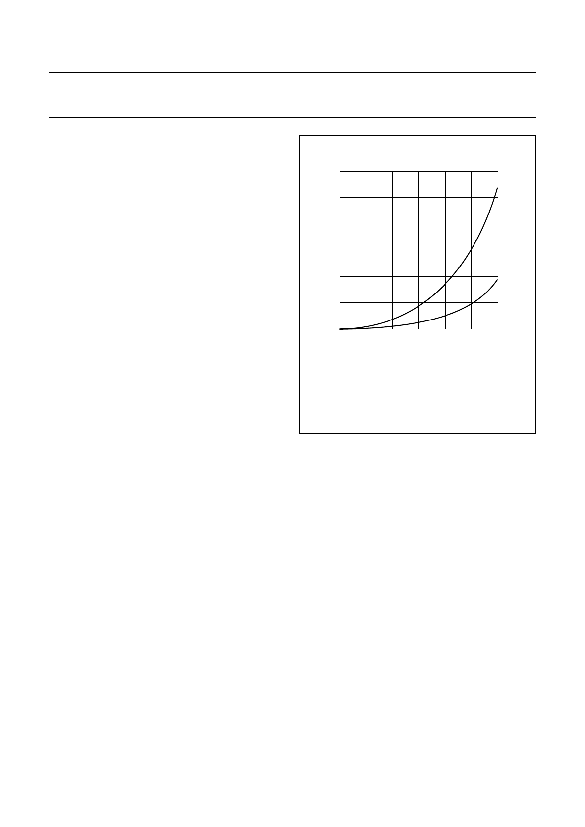
3
I
o(mod)(off)
(mA)
2
1
0
0 204060
(1) Worst case operation (Tj= 125 °C, VCC= 5.5 V
and worst case parameter processes).
(2) Typical operation.
Fig.9 I
o(mod)(off)
as a function of I
I
o(mod)(on)
TZA3041U
MGS902
(1)
(2)
(mA)
o(mod)(on)
.
The laser driver peak detectors are able to track MPD
output current overshoot and undershoot conditions.
Unfortunately, these conditions affect the ability of the IC
to correctly interpret the high and low level MPD current.
In particular, the occurrence of undershoot can have a
markedly adverse effect on the interpretation of the low
level MPD current.
Additional bias by modulation ‘off’ current
Although during operation, the full modulation current
switches between outputs LA and LAQ, a small amount of
modulation current continues to flow through the inactive
pin.
For example, when the laser,whose cathode is connected
to LA, is in the ‘dark’ part of its operating cycle (logic 0),
someof the modulation ‘off’ current flowsthrough LA while
most of the current flows through LAQ. This value
I
o(mod)(off)
is effectively added to the bias current and is
subtracted from the modulation current. Fortunately, the
value correlates closely with the magnitude of the
modulation current. Therefore, applications requiring low
bias and low modulation are less affected. Figure 9 shows
the modulation ‘off’ current as a function of the modulation
‘on’ current.
Monitoring the bias and modulation current
Although not recommended, the bias and modulation
currentsgenerated by the laser driver can be monitored by
measuring the voltages on pins TZERO and TONE,
respectively (see Fig.10). The relationship between these
voltages and the corresponding currents are given as
transconductance values and are specified in
Chapter “Characteristics”. The voltages on pins TZERO
and TONE range from 1.4 to 3.4 V. Any connection to
these pins should have a very high impedance value. It is
mandatory to use a CMOS buffer or an amplifier with an
input impedance higher than 100 GΩ and with an
extremely low input leakage current (pA).
2000 Feb 22 9
Philips Semiconductors Product specification
Gigabit Ethernet/Fibre Channel laser
drivers
handbook, halfpage
Automatic laser shut-down and laser slow start
TZERO, TONE
<
1 nA
<
1 nA
GND
40 pF
LINEAR VOLTAGE TO
CURRENT CONVERTER
2.4 V
MGS905
Fig.10 TZERO and TONE internal configuration.
TZA3041AHL; TZA3041BHL;
TZA3041U
Manual laser override
The automatic laser control function can be overridden by
connecting voltage sources to pins TZERO and TONE to
take direct control of the current sources for bias and
modulation respectively. The control voltages should
range from 1.4 to 3.4 V to swing the modulation current
over the range 1 to 60 mA and the bias current over the
range 1 to 90 mA. These current ranges are guaranteed.
Due to the tolerance range in the manufacturing process,
some devices may have higher current values than those
specified, as shown in Figs 12 and 13. Both figures show
thattemperature changes cause a slight tiltingof the linear
characteristic around an input voltage of 2.4 V.
Consequently, the manually controlled current level is
most insensitive to temperature variations at around this
value. Bias and modulation currents in excess of the
specified range are not supported and should be avoided.
Currentsintooroutofpins TZERO and TONE in excess of
10 µA must be avoided to prevent damage to the circuit.
The laser modulation and bias currents can be rapidly
switched off when a HIGH level (CMOS) is applied to
pin ALS. This function allows the circuit to be shut-down in
the event of an optical system malfunction. A 25 kΩ
pull-down resistor defaults pin ALS to the non active state
(see Fig.11).
When a LOW level is applied to pin ALS, the modulation
and bias currents slowly increase to the desired values at
the typical time constants of τ
ONE
and τ
, respectively.
ZERO
This can be used to slow-start the laser.
MGS911
V
CC(R)
handbook, halfpage
ALS
100 Ω
100 Ω
25 kΩ
GND
Fig.11 ALS input.
2000 Feb 22 10
 Loading...