

Philips tza3034 DATASHEETS

INTEGRATED CIRCUITS
DATA SH EET
TZA3034
SDH/SONET STM1/OC3
postamplifier
Product specification
Supersedes data of 1999 Mar 16
File under Integrated Circuits, IC19
1999 Nov 03
Philips Semiconductors Product specification
SDH/SONET STM1/OC3 postamplifier TZA3034
FEATURES
• PincompatiblewiththeNE/SA5224andNE/SA5225but
with extended power supply range and less external
component count
• Wideband operation from 1.0 kHz to 150 MHz typical
• Applicable in 155 Mbits/s SDH/SONET receivers
• Single supply voltage from 3.0 to 5.5 V
• Positive Emitter Coupled Logic (PECL) compatible data
outputs
• Programmable input signal level detection which can be
adjusted using a single external resistor
• On-chip DC offset compensation without external
capacitor.
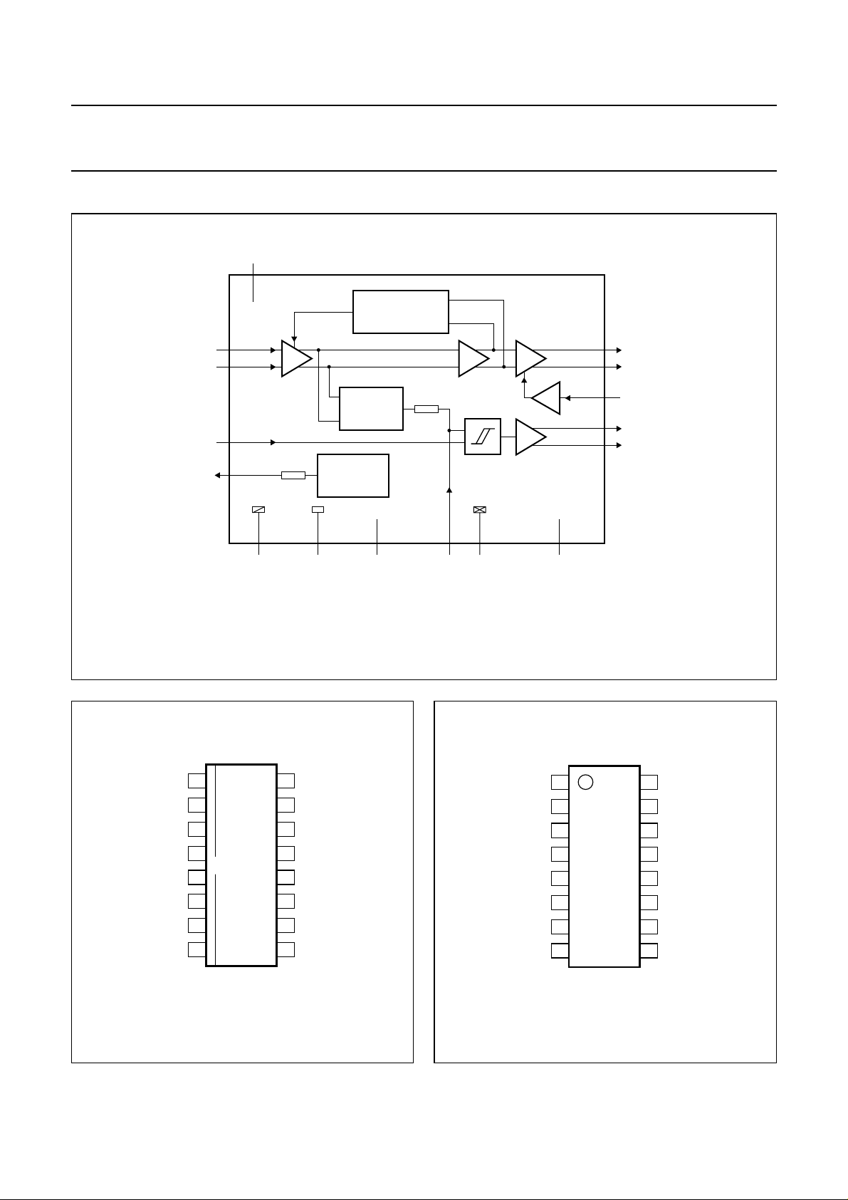
ORDERING INFORMATION
TYPE
NUMBER
TZA3034T SO16 plastic small outline package; 16 leads; body width 3.9 mm SOT109-1
TZA3034TT TSSOP16 plastic thin shrink small outline package; 16 leads; body width 4.4 mm SOT403-1
TZA3034U − bare die in waffle pack carriers; die dimensions 1.55 × 1.55 mm −
NAME DESCRIPTION VERSION
APPLICATIONS
• Digital fibre optic receiver in short, medium and long
haul optical telecommunications transmission systems
or in high speed data networks
• Wideband RF gain block.
GENERAL DESCRIPTION
The TZA3034 is a high gain limiting amplifier that is
designed to process signals from fibre optic preamplifiers
like the TZA3033. It is pin compatible with the NE/SA5224
and NE/SA5225 but with extended power supply range,
and needs less external components. Capable of
operating at 155 Mbits/s, the chip has input signal level
detection with a user-programmable threshold. The data
and level detection status outputs are differential outputs
for optimum noise margin and ease of use.
PACKAGE
1999 Nov 03 2
Philips Semiconductors Product specification
SDH/SONET STM1/OC3 postamplifier TZA3034
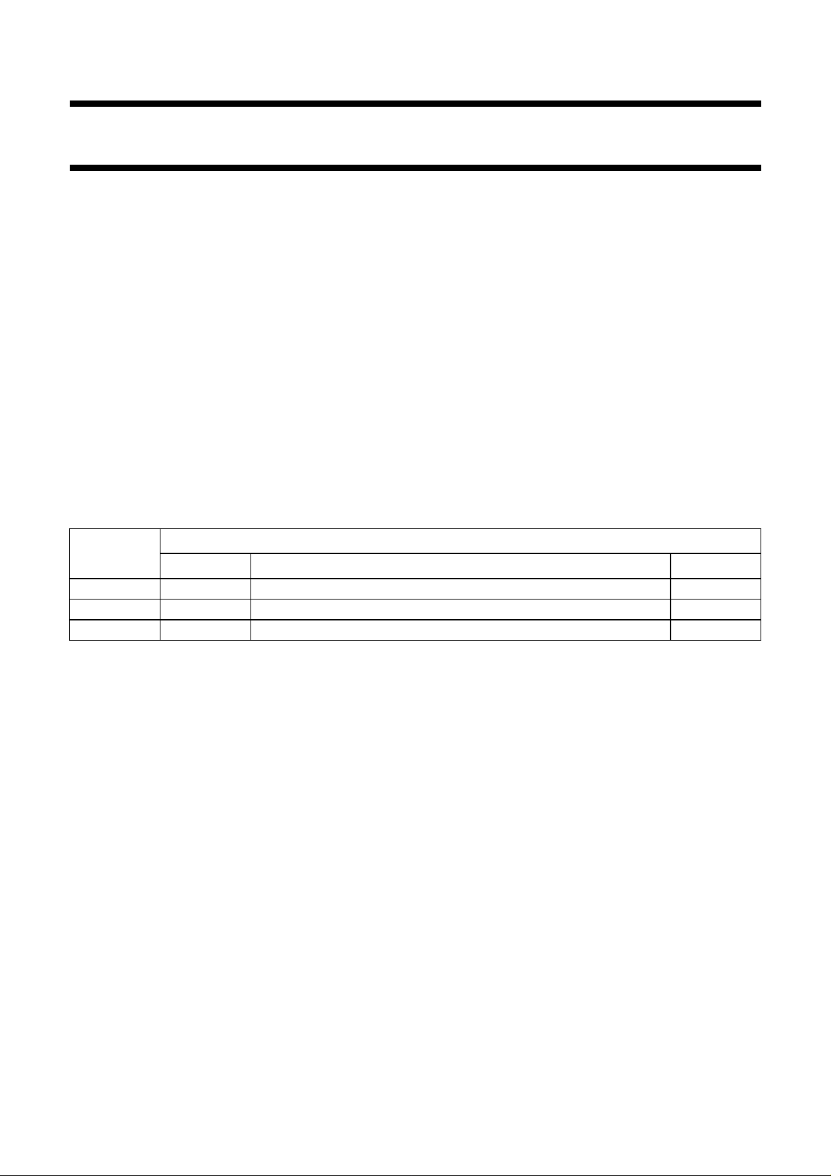
BLOCK DIAGRAM
ref
TEST
2
(2, 10, 15, 21, 26)
4 (7)
5 (8)
16 (30)
15 (29)
AGND V
A1 A2 A3
1 kΩ
(3, 4, 6, 9)
3
BAND GAP
REFERENCE
(1, 14)
1
SUB
DC-OFFSET
COMPENSATION
RECTIFIER
CCA
handbook, full pagewidth
DIN
DINQ
RSET
V
The numbers in brackets refer to the pad numbers of the bare die version.
Fig.1 Block diagram.
(11, 12)
6
25 kΩ
(19, 20, 22, 25)11(27, 28)
(13)
7
CF
DGND V
TZA3034
A4
CCD
(24) 13
(23) 12
(16) 8
(18) 10
(17) 9
14
DOUT
DOUTQ
JAM
ST
STQ
MGR281
handbook, halfpage
SUB
TEST
AGND
DIN
DINQ
V
CCA
CF
JAM
1
2
3
4
TZA3034T
5
6
7
8
MGR282
16
15
14
13
12
11
10
9
RSET
V
ref
V
CCD
DOUT
DOUTQ
DGND
ST
STQ
Fig.2 Pin configuration of TZA3034T.
1999 Nov 03 3
handbook, halfpage
Fig.3 Pin configuration of TZA3034TT.
SUB
TEST
AGND
DIN
DINQ
V
CCA
CF
JAM
1
2
3
4
TZA3034TT
5
6
7
8
MBK997
16
15
14
13
12
11
10
9
RSET
V
ref
V
CCD
DOUT
DOUTQ
DGND
ST
STQ

Philips Semiconductors Product specification
SDH/SONET STM1/OC3 postamplifier TZA3034
PINNING
SYMBOL
PIN
TZA3034T
TZA3034TT
PAD
TZA3034U
TYPE
(1)
DESCRIPTION
SUB 1 1, 14 S substrate pin; must be at the same potential as pin AGND
TEST 2 2, 10, 15,
− for test purpose only; to be left open in the application
21, 26
AGND 3 3, 4, 6, 9 S analog ground; must be at the same potential as pin DGND
DIN 4 7 I differential input; complementary to pin DINQ; DC bias level is set
internally at approximately 2.1 V
DINQ 5 8 I differential input; complementary to pin DIN; DC bias level is set
internally at approximately 2.1 V
V
CCA
6 11, 12 S analog supply voltage; must be at the same potential as pin V
CCD
CF 7 13 A input for connection of capacitor to set time constant of leveldetector
input filter (optional); the capacitor should be connected between
V
and pin CF
CCA
JAM 8 16 I PECL-compatible input; controls the output buffers,
pins DOUTand DOUTQ; when a LOW signal is applied, the output
bufferswill follow the input signal; when a HIGH signal is applied, the
output buffers will latch into LOW and HIGH states respectively;
when not connected, pin JAM is actively pulled LOW
STQ 9 17 O PECL-compatible status output of the input signal level detector;
when the input signal is below the user-programmed threshold level,
this output is HIGH; complementary to pin ST
ST 10 18 O PECL-compatible status output of the input signal level detector;
when the input signal is below the user-programmed threshold level,
this output is LOW; complementary to pin STQ
DGND 11 19, 20, 22,
S digital ground; must be at the same potential as pin AGND
25
DOUTQ 12 23 O PECL-compatible differential output; this pin will be forced into a
HIGH condition when pin JAM is HIGH; complementary to pin DOUT
DOUT 13 24 O PECL-compatible differential output; this pin will be forced into a
LOW condition when pin JAM is HIGH; complementary to
pin DOUTQ
V
V
CCD
ref
14 27, 28 S digital supply voltage; must be at the same potential as V
CCA
15 29 O band gap reference voltage; typical value is 1.2 V; internal series
resistor of 1 kΩ
RSET 16 30 A input signal level detector threshold setting; nominal DC voltage is
V
− 1.5 V;threshold level is set by connecting an external resistor
CCA
between V
and pin RSET or by forcing a current into pin RSET;
CCA
default value for this resistor is 180 kΩ which corresponds with
approximately 4 mV (p-p) differential input signal
n.c. − 5, 31, 32 − not connected
Note
1. Pin type abbreviations: O = Output, I = Input, S = power Supply and A = Analog function.
1999 Nov 03 4

Philips Semiconductors Product specification
SDH/SONET STM1/OC3 postamplifier TZA3034
FUNCTIONAL DESCRIPTION
The TZA3034 accepts up to 155 Mbits/s SDH/SONET
data streams, with amplitudes from2 mV up to 1.5 V (p-p)
single-ended. The input signal will be amplified andlimited
to differential PECL output levels (see Fig.1).
The input buffer A1 presents an impedance of
approximately 4.5 kΩ to the data stream on the inputs
pin DIN and pin DINQ. The input can be used both
single-ended and differential, but differential operation is
preferred for better performance.
Because of the high gain of the postamplifier, a very small
offset voltage would shift the decision level in such a way
that the input sensitivity decreases drastically. Therefore a
DC offset compensation circuit is implemented in the
TZA3034, which keeps the input of buffer A3 at its toggle
point in the absence of any input signal.
An input signal level detection is implemented to check if
the input signal is above the user-programmed level.
The outcome of this test is available at the PECL outputs,
pins ST and STQ. This flag can also be used to prevent
the PECL outputs pins DOUT and DOUTQ from reacting
to noise in the absence of a valid input signal, by
connecting pin STQ to pin JAM. This guarantees that data
willonly be transmitted when the input signal-to-noise ratio
is sufficient for low bit error rate system operation.
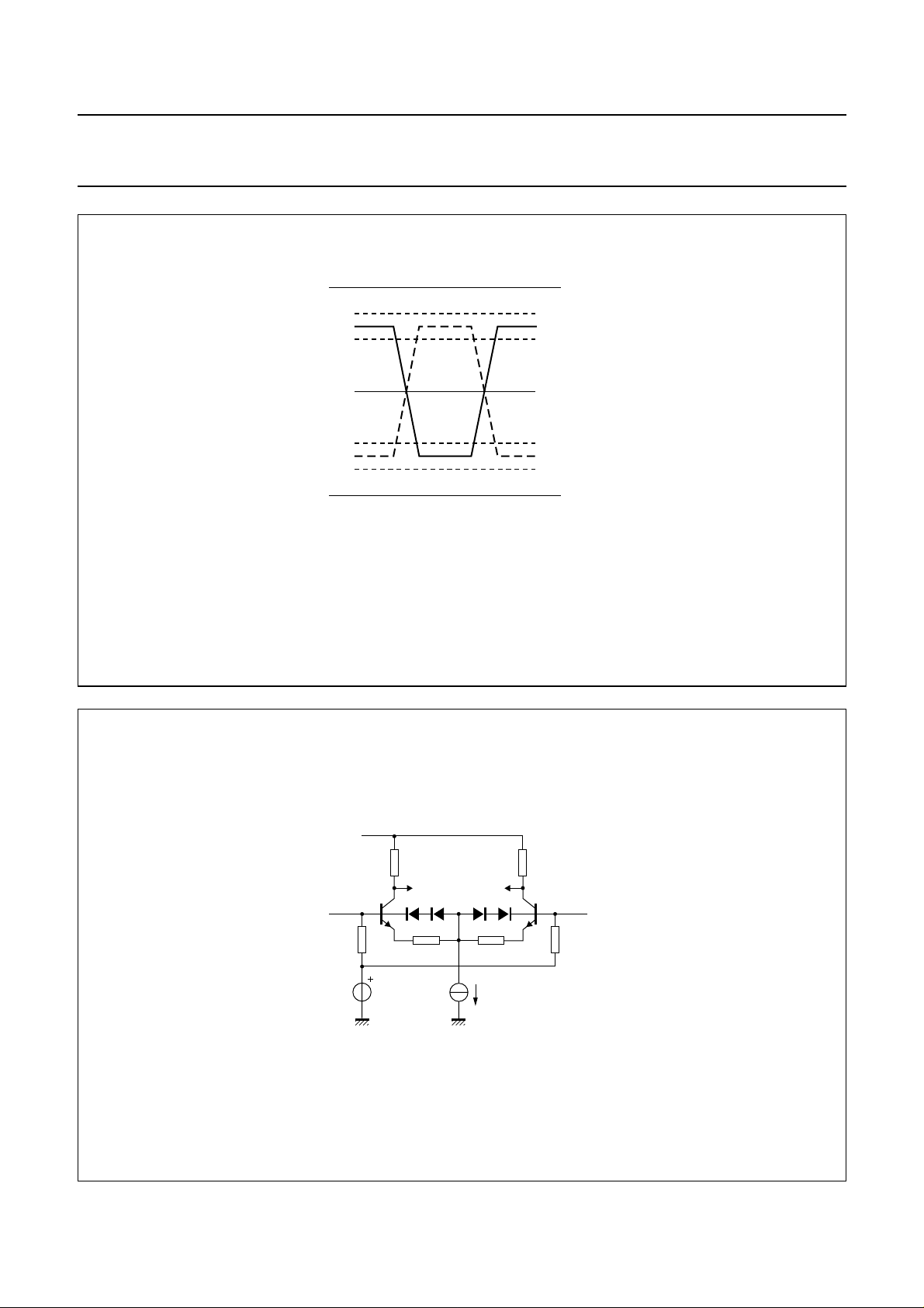
PECL logic
The logic level symbol definitions for PECL are shown in
Fig.4.
Input biasing
The inputs, pins DIN and DINQ, are DC biased at
approximately 2.1 V by an internal reference generator
(see Fig.5). The TZA3034 can be DC coupled, but
AC coupling is preferred. In case of DC coupling, the
driving source must operate within the allowable input
signal range (1.3 V to V
). Also a DC offset voltage of
CCA
more than a few millivolts should be avoided, since the
internal DC offset compensation circuit has a limited
correction range.
If AC coupling is used to remove any DC compatibility
requirement, the coupling capacitors must be large
enough to pass the lowest input frequency of interest.
For example, 1 nF coupling capacitors react with the
internal 4.5 kΩ input bias resistors to yield a lower −3dB
frequency of 35 kHz. This then sets a limit on the
maximum number of consecutive pulses that can be
sensed accurately at the system data rate. Capacitor
tolerance and resistor variation must be included for an
accurate calculation.
DC-offset compensation
A control loop connected between the inputs of buffer A3
andamplifier A1 (see Fig.1) will keep theinputof buffer A3
at its toggle point in the absence of any input signal.
Because of the active offset compensation which is
integrated in the TZA3034, no external capacitor is
required. The loop time constant determines the lower
cut-off frequency of the amplifier chain, which is set at
approximately 850 Hz.
Input signal level detection
The TZA3034 allows for user-programmable input signal
leveldetectionand can automatically disable the switching
of the PECL outputs if the input signal is below a set
threshold. This prevents the outputs from reacting to noise
in the absence of avalid input signal, and insures that data
will only be transmitted when the signal-to-noise ratio of
the input signal is sufficient for low bit-error-rate system
operation.ComplementaryPECLflags(pins ST and STQ)
indicate whether the input signal is above or below the
programmed threshold level.
The input signal is amplified and rectified before being
compared to a programmable threshold reference. A filter
isincluded to prevent noise spikes from triggeringthe level
detector. This filter has a nominal 1 µs time constant and
additional filtering can be achieved by using an external
capacitor between V
and pin CF (the internal driving
CCA
impedance nominally is 25 kΩ). The resultant signal is
then compared to a threshold current through pin RSET.
This current can be set by connecting an external resistor
between V
and pin RSET, or by forcing a current into
CCA
pin RSET (see Fig.6).
1999 Nov 03 5

Philips Semiconductors Product specification
SDH/SONET STM1/OC3 postamplifier TZA3034
The relationship between the threshold current and the
detected input voltage is approximately:
I
RSET
0.0018 V
–()A[]×=
DINVDINQ
(1)
In the formulas (1) and (3), the voltage on pin DIN and
pin DINQ is measured as peak-to-peak value.
Since the voltage on pin RSET is held constant at 1.5 V
below V
I
RSET
, the current flowing into this pin will be:
CCA
1.5
A[]=
------------R
ADJ
(2)
Combining these two formulas results in a generalformula
to calculate R
R
ADJ
--------------------------------------- -
for a given input signal level detection:
ADJ
830
V
–()
DINVDINQ
Ω[]=
(3)
Example: Detection should occur if the differential voltage
of the input signals drops below 4 mV (p-p). In this case, a
reference current of 0.0018 × 0.004 = 7.2 µA should flow
into pin RSET. This can be set using a current source or
simply by connecting a resistor of the appropriate value.
The resistor must be connected between V
CCA
and
pin RSET. In this example the value would be:
R
ADJ
830
-------------- -
0.004
207.5 kΩ==
The hysteresis is fixed internally at 3 dB electrical. In the
example of above, a differential level below 4 mV (p-p) of
the input signal will drive pin ST to LOW, and an input
signal level above 5.7 mV (p-p) will drive pin ST to HIGH.
Dissipation
Since the thermal resistance from junction to ambient
of the TSSOP package is higher than the thermal
R
th(j-a)
resistance of the SO package (see Chapter “Thermal
characteristics”), the dissipation should be considered
when using the TZA3034TT version.
The formula to calculate the worst case die temperature is:
T
T
j
ambRth j a–()
+=
P×
max
(4)
where
T
= junction temperature
j
T
= ambient temperature
amb
R
= thermal resistance from junction to ambient
th(j-a)
P
= maximum power dissipation.
max
For the TZA3034T (SO package), the worst case die
temperatureTj=85+115×0.3 = 119.5 °Cwhichis below
the maximum operating temperature.
For the TZA3034TT (TSSOP package), the worst casedie
temperature Tj=85+150×0.3 = 130 °C which is higher
than the maximum operating temperature, and therefore
strongly discouraged. It is recommended to lower the
thermalresistancefromjunctiontoambient, e.g. by means
of a dedicated board layout.
However, if the ambient temperature is limited to 75 °Cor
the power supply is limited to 3.3 ±0.3 V, the junction
temperature will stay below the maximum value without
further precautions.
A function is provided to automatically disable the signal
transmission when the chip senses that the input signal is
below the programmed threshold level. This function can
be put into operation by connecting pin JAM with pin STQ.
When the input signal is below the programmed threshold
level, the data outputs are then forced to a predetermined
state (pin DOUT = LOW and pin DOUTQ = HIGH).
Response time of the input signal level detection circuit is
determined by the time constant of the input capacitors,
together with the filter time constant (1 µs internal plus the
additional capacitor at pin CF). For SDH/SONET
applications, couple capacitors of 1.5 nF are
recommended, leading to a high-pass frequency of
approximately 30 kHz and a maximum assert time of
30 µs.
1999 Nov 03 6
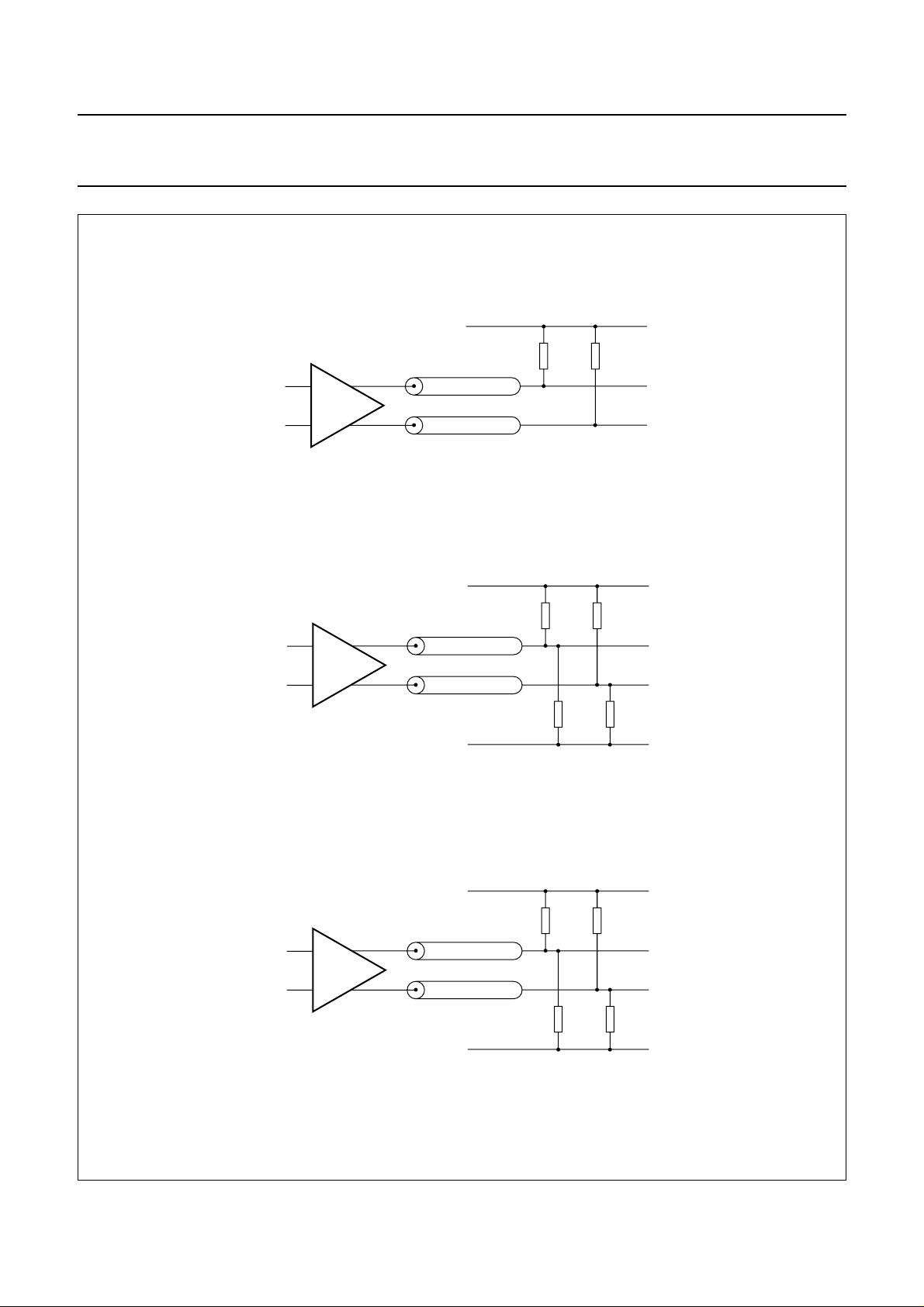
PECL output circuits
The output circuit of ST and STQ is given in Fig.7.
The output circuit of DOUT and DOUTQ is given in Fig.8.
Some PECL termination schemes are given in Fig.9.
Philips Semiconductors Product specification
SDH/SONET STM1/OC3 postamplifier TZA3034
handbook, halfpage
(1)
(2)
(1) Output signal on pins DOUT or ST; complementary to output signal (2).
(2) Output signal on pins DOUTQ or STQ; complementary to output signal (1)
Fig.4 Logic level symbol definitions for PECL outputs.
V
V
V
V
MGS812
V
CC
OH(max)
OH(min)
OL(max)
OL(min)
GND
DIN
V
4.5 kΩ
CC
2.1 V
handbook, halfpage
Fig.5 Data input circuit DIN and DINQ.
1999 Nov 03 7
DINQ
4.5 kΩ
1 mA
MGR958
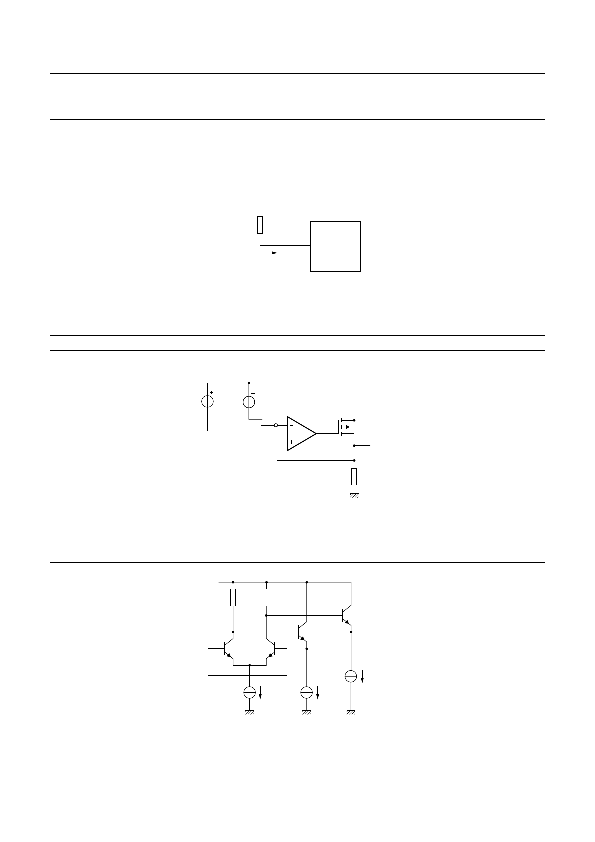
Philips Semiconductors Product specification
SDH/SONET STM1/OC3 postamplifier TZA3034
V
RSET=VCCA
− 1.5 V.
handbook, halfpage
Fig.6 level detect input circuit RSET.
handbook, halfpage
V
LOW
V
RSET
V
CCA
V
HIGH
R
ADJ
RSET
I
RSET
V
TZA3034
MGS813
CC
ST
10 kΩ
Output STQ is complementary to output ST.
Fig.7 PECL output circuit ST and STQ.
V
handbook, halfpage
CC
105 Ω 105 Ω
9 mA
Fig.8 PECL output circuit DOUT and DOUTQ.
1999 Nov 03 8
MGS814
DOUT
DOUTQ
0.5 mA
0.5 mA
MGR247
Philips Semiconductors Product specification
SDH/SONET STM1/OC3 postamplifier TZA3034
handbook, full pagewidth
handbook, full pagewidth
VCC − 2 V
R1 = 50 Ω R1 = 50 Ω
V
V
I
V
IQ
V
I
V
IQ
O
Zo = 50 Ω
V
OQ
VCC = 3.3 V
R1 = 127 Ω
V
O
Zo = 50 Ω
V
OQ
R2 = 82.5 Ω
GND
MGR248
R1 = 127 Ω
R2 = 82.5 Ω
MGR249
handbook, full pagewidth
V
V
I
V
IQ
O
Zo = 50 Ω
V
OQ
Fig.9 PECL output termination schemes.
1999 Nov 03 9
VCC = 5.0 V
R1 = 83.3 Ω
R2 = 125 Ω
GND
R1 = 83.3 Ω
R2 = 125 Ω
MGR250
 Loading...