

Philips TZA3033T Datasheet

INTEGRATED CIRCUITS
DATA SH EET
TZA3033
SDH/SONET STM1/OC3
transimpedance amplifier
Objective specification
File under Integrated Circuits, IC19
1998 Jul 08
Philips Semiconductors Objective specification
SDH/SONET STM1/OC3 transimpedance amplifier TZA3033
FEATURES
• Low equivalent input noise, typically 1 pA/√Hz
• Wide dynamic range, typically 0.25 µA to 1.6 mA
• Differential transimpedance of 117 kΩ
• Bandwidth minimum 150 MHz
• Differential outputs
• On-chip AGC (Automatic Gain Control)
• No external components required
• Single supply voltage from 3.0 to 5.5 V
• Bias voltage for PIN diode
• Pin compatible with SA5223.
APPLICATIONS
• Digital fibre optic receiver in short, medium and long
haul optical telecommunications transmission systems
or in high speed data networks
• Wideband RF gain block.
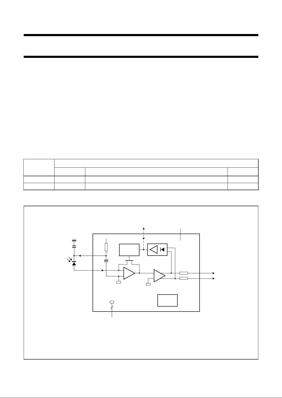
GENERAL DESCRIPTION
The TZA3033 is a low-noise transimpedance amplifier with
AGC designed to be used in STM1/OC3 fibre optic links.
It amplifies the current generated by a photo detector
(PIN diode or avalanche photodiode) and converts it to a
differential output voltage.
ORDERING INFORMATION
TYPE
NUMBER
NAME DESCRIPTION VERSION
PACKAGE
TZA3033T SO8 plastic small outline package; 8 leads; body width 3.9 mm SOT96-1
TZA3033U naked die die in waffle pack carriers; die dimensions 0.960 × 1.210 mm −
BLOCK DIAGRAM
handbook, full pagewidth
V
CC
1 nF
1 (1)
DREF
3 (5)IPhoto
(1) AGC analog I/O is only available on the TZA3033U (pad 15).
The numbers in brackets refer to the pad numbers of the naked die version.
2 kΩ
65 pF
3
GND
GAIN
CONTROL
A1
low noise
TZA3033
2, 4, 5 (3, 4, 7, 8, 9, 10)
Fig.1 Block diagram.
(1)
AGC
peak detector
A2
amplifier single-ended to
differential converter
BIASING
V
CC
8 (13, 14)(15)
(12) 7 OUTQ
(11) 6 OUT
MGR368
1998 Jul 08 2
Philips Semiconductors Objective specification
SDH/SONET STM1/OC3 transimpedance amplifier TZA3033
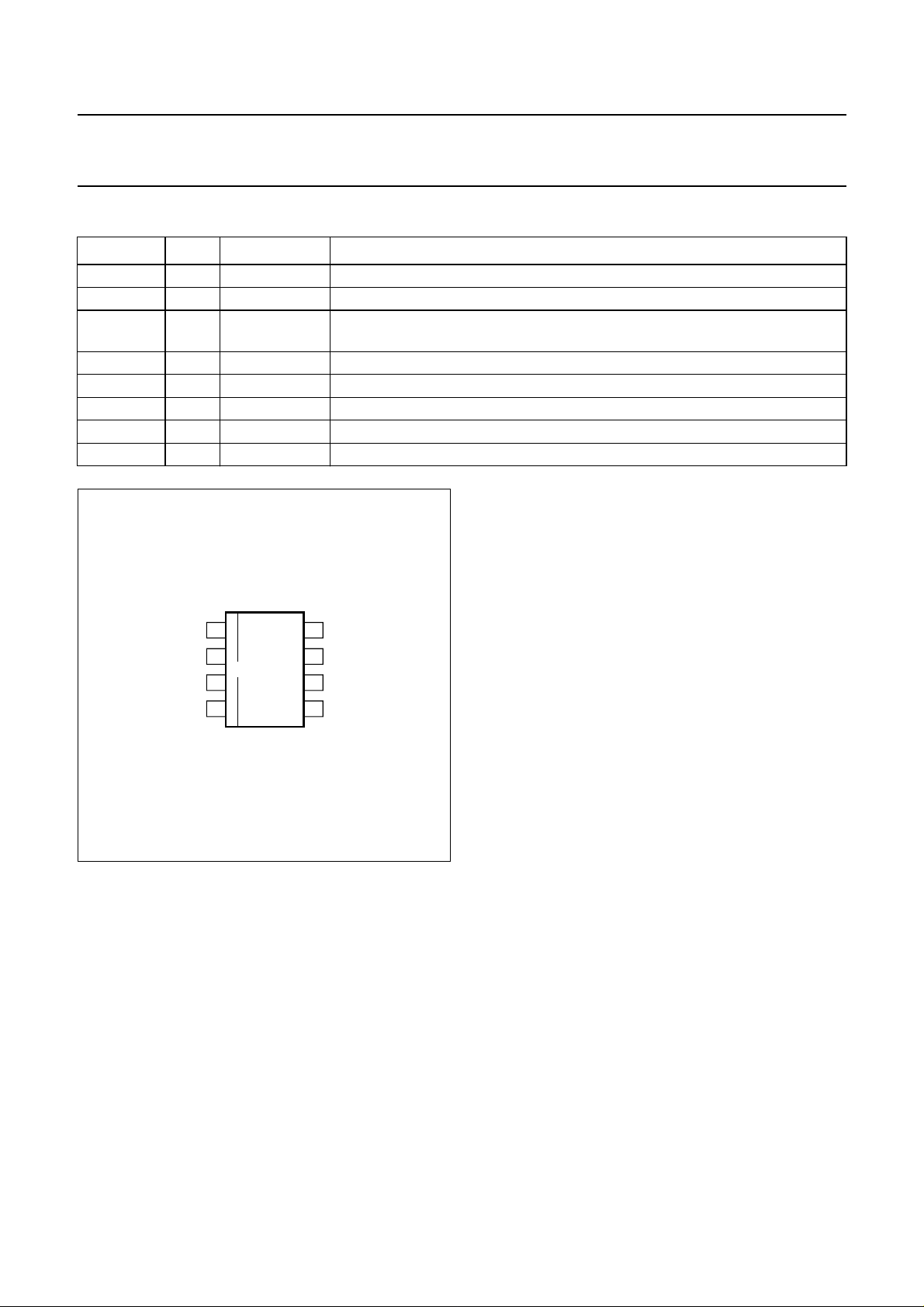
PINNING
SYMBOL PIN TYPE DESCRIPTION
DREF 1 analog output bias voltage for PIN diode (V
GND 2 ground ground
IPhoto 3 analog input current input; anode of PIN diode should be connected to this pin; DC bias
voltage is 1048 mV
GND 4 ground ground
GND 5 ground ground
OUT 6 data output data output; OUT goes HIGH when current flows into IPhoto (pin 3)
OUTQ 7 data output compliment of OUT (pin6)
V
CC
8 supply supply voltage
); cathode should be connected to this pin
CC
handbook, halfpage
DREF
1
2
TZA3033T
3
IPhoto
4
GND
MGR369
Fig.2 Pin configuration.
V
8
CC
OUTQGND
7
OUT
6
GND
5
1998 Jul 08 3
Philips Semiconductors Objective specification
SDH/SONET STM1/OC3 transimpedance amplifier TZA3033
PAD CONFIGURATION
Bonding pad locations
handbook, full pagewidth
18
DREF
V
CC
GND
IPhoto
GND
Pad 15 (AGC) is not bonded.
2
TESTA
TESTB
36
AGC
15
1
2
3
TZA3033U
4
5
6
7
89
7
OUTQ
13
14
12
11
10
OUT
GND
45
MGR371
Fig.3 Bonding diagram TZA3033U.
1998 Jul 08 4
Philips Semiconductors Objective specification
SDH/SONET STM1/OC3 transimpedance amplifier TZA3033
Pad centre locations
COORDINATES
(1)
SYMBOL PAD
xy
DREF 1 95 881
TESTA 2 95 735
GND 3 95 618
GND 4 95 473
IPhoto 5 95 285
TESTB 6 95 147
GND 7 215 95
GND 8 360 95
GND 9 549 95
GND 10 691 95
OUT 11 785 501
OUTQ 12 785 641
V
CC
V
CC
13 567 1055
14 424 1055
AGC 15 259 1055
Note
1. All coordinates (µm) are measured with respect to the
bottom left-hand corner of the die.
FUNCTIONAL DESCRIPTION
The TZA3033 is a transimpedance amplifier intended for
use in fibre optic links for signal recovery in STM1/OC3
applications. It amplifies the current generated by a photo
detector (PIN diode or avalanche photodiode) and
transforms it into a differential output voltage. The most
important characteristics of the TZA3033 are high receiver
sensitivity and wide dynamic range.
High receiver sensitivity is achieved by minimizing noise in
the transimpedance amplifier.
The signal current generated by a PIN diode can vary
between 0.25 µA to 1.6 mA (peak-to-peak value).
An AGC loop (see Fig.1) is implemented to make it
possible to handle such a wide dynamic range.
The AGC loop increases the dynamic range of the
receiver by reducing the feedback resistance of the
preamplifier. The AGC loop hold capacitor is integrated
on-chip, so an external capacitor is not needed for AGC.
The AGC voltage can be monitored at pad 15 on the naked
die (TZA3033U). Pad 15 is not bonded in the packaged
device (TZA3033T). This pad can be left unconnected
during normal operation. It can also be used to force an
external AGC voltage. If pad 15 (AGC) is connected to
, the internal AGC loop is disabled and the receiver
V
CC
gain is at a maximum. The maximum input current is then
about 10 µA.
A differential amplifier converts the output of the
preamplifier to a differential voltage. The data output circuit
is given in Fig.4.
The logic level symbol definitions are shown in Fig.5.
1998 Jul 08 5
 Loading...