

Philips TZA3030HL, TZA3030U, TZA3024T Datasheet

DATA SH EET
Objective specification
File under Integrated Circuits, IC19
1998 Aug 24
INTEGRATED CIRCUITS
TZA3030
SDH/SONET STM1/OC3 optical
receiver
1998 Aug 24 2
Philips Semiconductors Objective specification
SDH/SONET STM1/OC3 optical receiver TZA3030
FEATURES
• Low equivalent input noise, typically 1 pA/√Hz
• Wide dynamic range, typically 0.5 µAto2mA
• On-chip low-pass filter. The bandwidth can be varied
between 90 and 150 MHz using an external resistor.
Default value is 120 MHz.
• Differential transimpedance of 1.8 MΩ
• On-chip Automatic Gain Control (AGC)
• Positive Emitter Coupled Logic (PECL) or
Current-Mode Logic (CML) compatible data outputs
• LOS (Loss Of Signal) detection
• LOS threshold level can be adjusted using a single
external resistor
• On-chip DC offset compensation
• Single supply voltage from 3.0 to 5.5 V
• Bias voltage for PIN diode.
APPLICATIONS
• Digital fibre optic receiver in short, medium and long
haul optical telecommunications transmission systems
or in high speed data networks
• Wideband RF gain block.
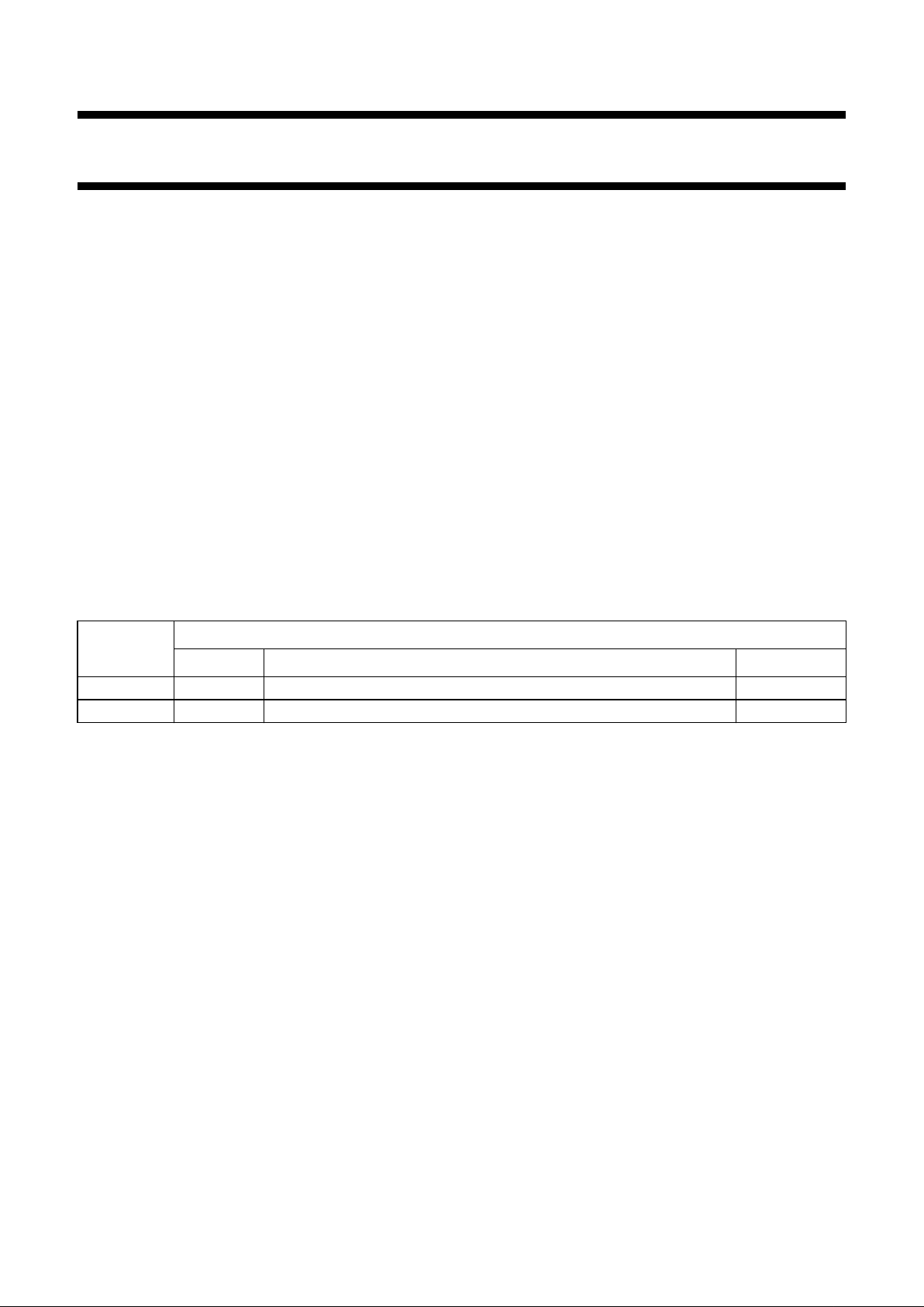
GENERAL DESCRIPTION
The TZA3030 optical receiver is a low-noise
transimpedance amplifier with AGC plus a limiting
amplifier designed to be used in SDH/SONET fibre optic
links. The TZA3030 amplifies the current generated by a
photo detector (PIN diode or avalanche photodiode) and
converts it to a differential output voltage.
ORDERING INFORMATION
TYPE
NUMBER
PACKAGE
NAME DESCRIPTION VERSION
TZA3030HL LQFP32 plastic low profile quad flat package; 32 leads; body 5 × 5 × 1.4 mm SOT401-1
TZA3030U − naked die in waffle pack carriers; die dimensions 1.58 × 1.58 mm −
1998 Aug 24 3
Philips Semiconductors Objective specification
SDH/SONET STM1/OC3 optical receiver TZA3030
BLOCK DIAGRAM
Fig.1 Block diagram.
handbook, full pagewidth
MBK857
GAIN
CONTROL
TESTING
BIASING
2 2
A1 A2
4
2, 5 17, 2031
DREF
2
kΩ
7
65 pF
IPhoto
PREAMPLIFIER
LOS DETECTION
LIMITING
AMPLIFIER
DC OFFSET
COMPENSATION
V
CCA
V
CCD
5
13, 16, 21
24, 25
DGND
7
1, 3, 6, 8
9, 30, 32
AGNDSUB
1412
RFTEST
11
V
ref
10
BWC
AGC
PEAK DETECTOR
TZA3030
CML
PECL
TTL
29
LOSTH
26 LOS
28
LOSTTL
18 OUTCML
19 OUTQCML
15
OUTSEL
22 OUTPECL
23
OUTQPECL
27
LOSQ
PECL
1 nF
1998 Aug 24 4
Philips Semiconductors Objective specification
SDH/SONET STM1/OC3 optical receiver TZA3030
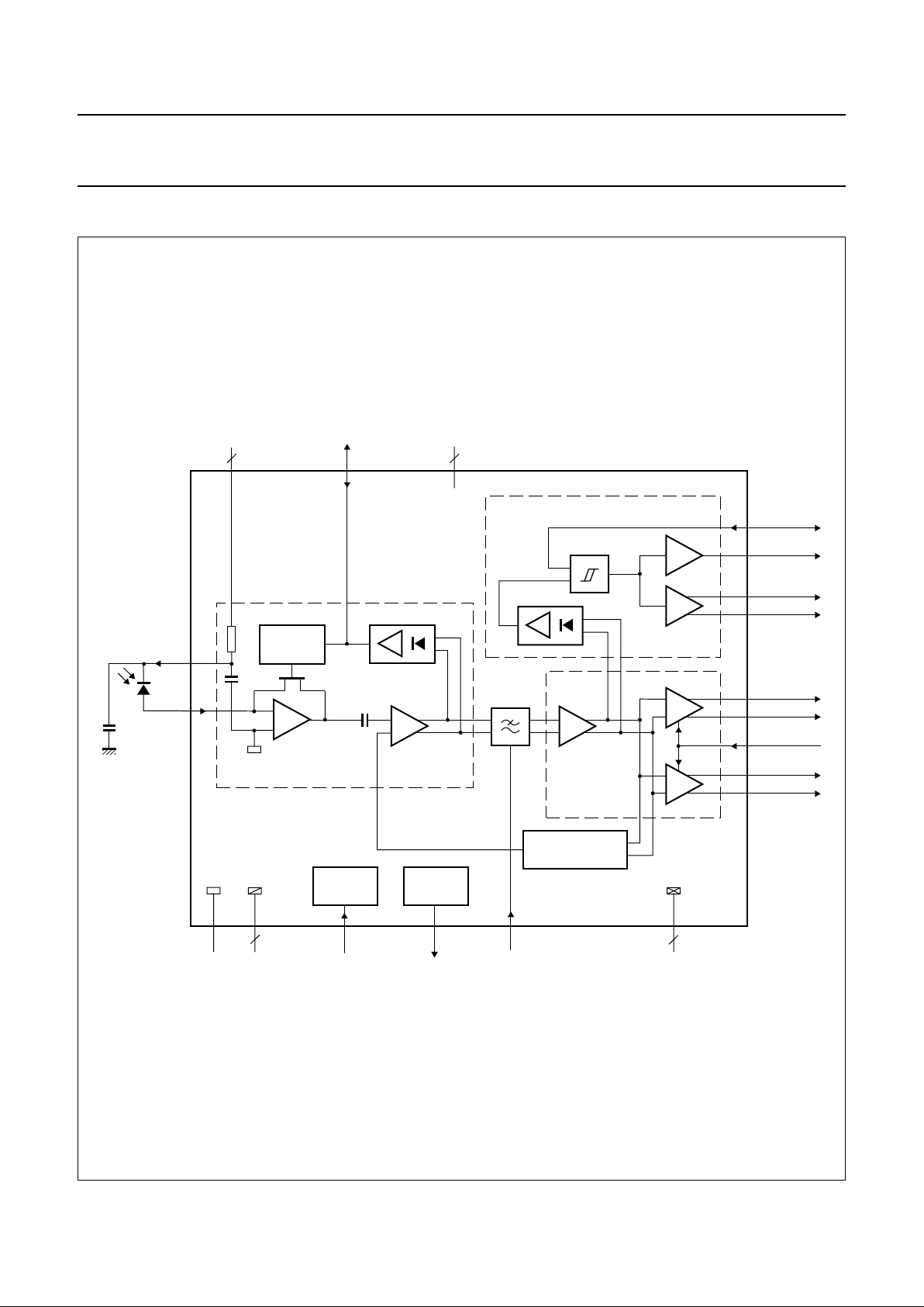
PINNING
SYMBOL PIN TYPE DESCRIPTION
AGND 1 ground analog ground
V
CCA
2 supply analog supply voltage
AGND 3 ground analog ground
DREF 4 analog output bias voltage for PIN diode (V
CCA
); cathode should be connected to this pin
V
CCA
5 supply analog supply voltage
AGND 6 ground analog ground
IPhoto 7 analog input current input; connect the anode of PIN diode to this pin; DC bias level is
1048 mV
AGND 8 ground analog ground
AGND 9 ground analog ground
BWC 10 analog input bandwidth control pin; default bandwidth is 120 MHz; a resistor should be
connected between V
ref
(pin 11) and BWC (pin 10) to decrease bandwidth, or
between BWC (pin 10) and AGND to increase bandwidth
V
ref
11 analog output band gap reference voltage; nominal value approximately 1.2 V
SUB 12 substrate substrate pin; to be connected to AGND
DGND 13 ground digital ground
RFTEST 14 analog input test pin; not connected; not used in application
OUTSEL 15 CMOS input output select pin; when OUTSEL is HIGH, CML data outputs are active and
PECL data outputs are disabled; OUTSEL is pulled LOW if left unconnected,
PECL data outputs will then be active and CML data outputs disabled
DGND 16 ground digital ground
V
CCD
17 supply digital supply voltage
OUTCML 18 CML output CML data output; OUTCML goes HIGH when current flows into IPhoto (pin 7)
OUTQCML 19 CML output CML compliment of OUTCML (pin 18)
V
CCD
20 supply digital supply voltage
DGND 21 ground digital ground
OUTPECL 22 PECL output PECL data output; OUTPECL goes HIGH when current flows into IPhoto (pin 7)
OUTQPECL 23 PECL output PECL compliment of OUTPECL (pin 22)
DGND 24 ground digital ground
DGND 25 ground digital ground
LOS 26 PECL output PECL-compatible LOS detection pin; LOS output is HIGH when the input signal
is below the user programmable threshold level
LOSQ 27 PECL output PECL compliment of LOS (pin 26)
LOSTTL 28 TTL output CMOS-compatible LOS detection pin; the LOSTTL output is HIGH when the
input signal is below the user programmable threshold level
LOSTH 29 analog I/O pin for setting input threshold level; nominal DC voltage is V
CCA
− 1.5 V;
threshold level set by connecting an external resistor between LOSTH and
V
CCA
or by forcing a current into LOSTH; default value for this resistor is 400 kΩ
AGND 30 ground analog ground
AGC 31 analog I/O AGC monitor voltage; the internal AGC circuit can be disabled by applying an
external voltage to this pin
AGND 32 ground analog ground
1998 Aug 24 5
Philips Semiconductors Objective specification
SDH/SONET STM1/OC3 optical receiver TZA3030
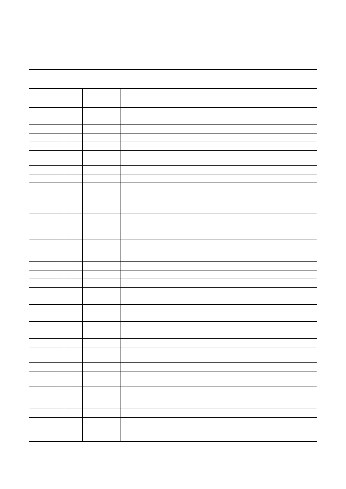
Fig.2 Pin configuration.
handbook, full pagewidth
TZA3030HL
MBK856
1
2
3
4
5
6
7
8
24
23
22
21
20
19
18
17
9
10
11
12
13
14
15
16
32
31
30
29
28
27
26
25
AGND
V
CCA
AGND
DREF
V
CCA
AGND
IPhoto
AGND
DGND
LOS
LOSQ
LOSTTL
LOSTH
AGND
AGC
AGND
V
CCD
OUTCML
V
CCD
DGND
OUTPECL
DGND
OUTQPECL
OUTQCML
AGND
BWC
V
ref
SUB
RFTEST
OUTSEL
DGND
DGND
1998 Aug 24 6
Philips Semiconductors Objective specification
SDH/SONET STM1/OC3 optical receiver TZA3030
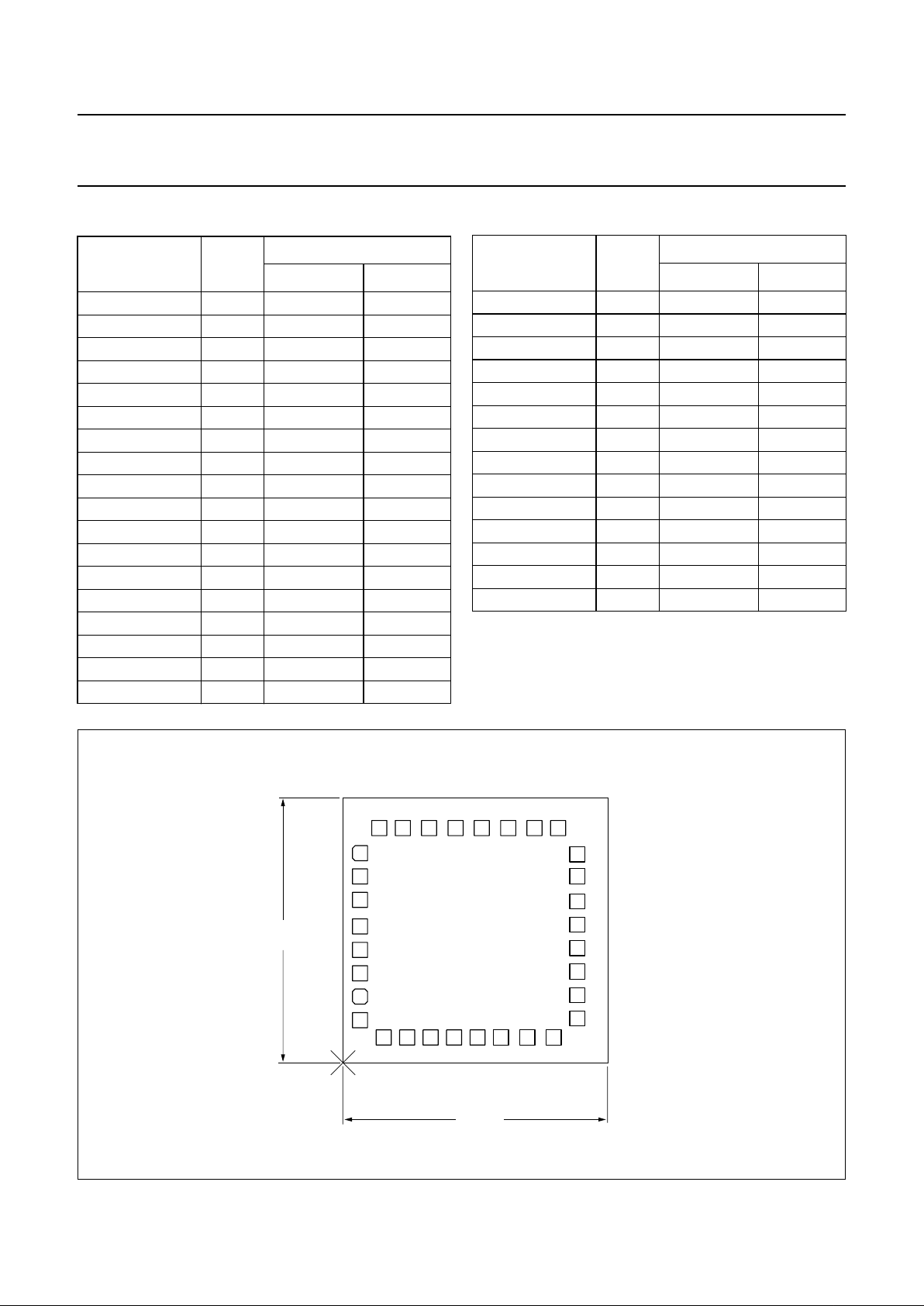
CHIP DIMENSIONS AND BONDING PAD LOCATIONS
SYMBOL PAD
COORDINATES
(1)
xy
AGND 1 102 1251
V
CCA
2 102 1111
AGND 3 102 971
DREF 4 102 814
V
CCA
5 102 674
AGND 6 102 534
IPhoto 7 102 395
AGND 8 102 254
AGND 9 243 105
BWC 10 383 105
V
ref
11 523 105
SUB 12 663 105
DGND 13 803 105
RFTEST 14 943 105
OUTSEL 15 1100 105
DGND 16 1257 105
V
CCD
17 1398 263
OUTCML 18 1398 403
Note
1. All coordinates (µm) are measured with respect to the
bottom left-hand corner of the die.
OUTQCML 19 1398 543
V
CCD
20 1398 683
DGND 21 1398 823
OUTPECL 22 1398 963
OUTQPECL 23 1398 1103
DGND 24 1398 1243
DGND 25 1283 1400
LOS 26 1143 1400
LOSQ 27 986 1400
LOSTTL 28 829 1400
LOSTH 29 671 1400
AGND 30 514 1400
AGC 31 357 1400
AGND 32 217 1400
SYMBOL PAD
COORDINATES
(1)
xy
Fig.3 Bonding pad locations of TZA3030U.
handbook, full pagewidth
AGND 1
DGND
24
OUTQPECL23
OUTPECL22
DGND21
V
CCD
20
OUTQCML19
OUTCML18
V
CCD
17
AGND
3
DREF 4
V
CCA
5
AGND 6
IPhoto 7
AGND 8
V
CCA
2
TZA3030U
9
AGND
32
AGND31AGC30AGND29LOSTH28LOSTTL27LOSQ26LOS25DGND
10
BWC
11
V
ref
12
SUB
13
DGND
14
RFTEST
15
OUTSEL
16
DGND
MBK858
y
1.58 mm
x
0
0
1.58
mm
 Loading...