

Philips TZA3023U, TZA3023T Datasheet

INTEGRATED CIRCUITS
DATA SH EET
TZA3023
SDH/SONET STM4/OC12
transimpedance amplifier
Objective specification
File under Integrated Circuits, IC19
1997 Oct 17
Philips Semiconductors Objective specification
SDH/SONET STM4/OC12
TZA3023
transimpedance amplifier
FEATURES
• Low equivalent input noise, typically 3.5 pA/√Hz
• Wide dynamic range, typically 1 µA to 1.5 mA
• Differential transimpedance of 21 kΩ
• Wide bandwidth: 600 MHz
• Differential outputs
• On-chip AGC (Automatic Gain Control)
• No external components required
• Single supply voltage from 3.0 to 5.5 V
• Bias voltage for PIN diode.
ORDERING INFORMATION
TYPE
NUMBER
NAME DESCRIPTION VERSION
TZA3023T SO8 plastic small outline package; 8 leads; body width 3.9 mm SOT96-1
TZA3023U naked die die in waffle pack carriers; die dimensions 0.960 × 1.210 mm −
APPLICATIONS
• Digital fibre optic receiver in short, medium and long
haul optical telecommunications transmission systems
or in high speed data networks
• Wideband RF gain block.
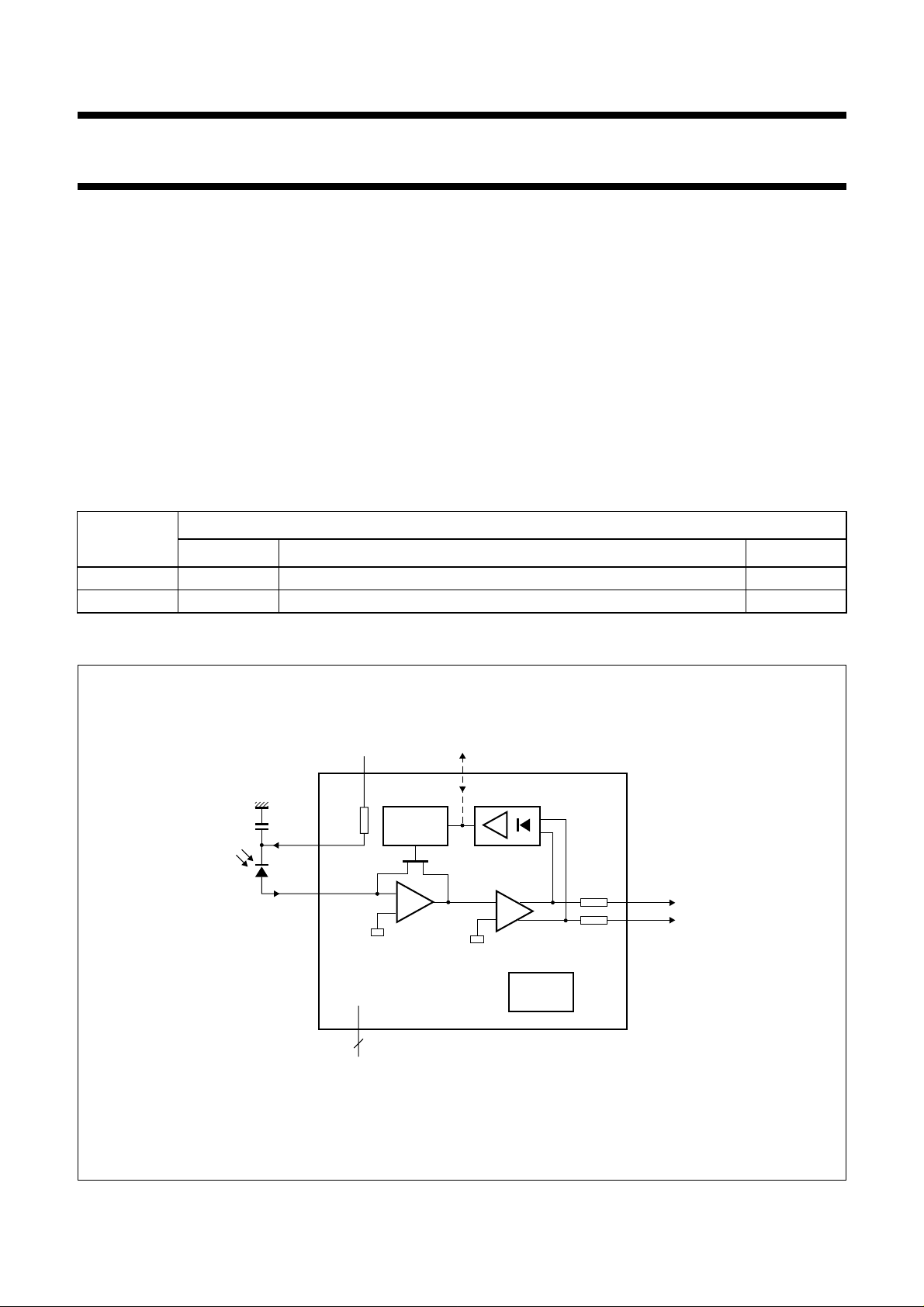
DESCRIPTION
The TZA3023 is a low-noise transimpedance amplifier with
AGC designed to be used in STM4/OC12 fibre optic links.
It amplifies the current generated by a photo detector (PIN
diode or avalanche photodiode) and converts it to a
differential output voltage.
PACKAGE
BLOCK DIAGRAM
handbook, full pagewidth
DREF
(1)
V
CC
8
2
kΩ
1
3IPhoto
CONTROL
TZA3023T
2, 4, 5
3
GND
AGC
peak detector
GAIN
A1
low noise
amplifier single ended to
differential converter
BIASING
7 OUTQ
6 OUT
MGK918
(1) AGC analog I/O is only available on the TZA3023U (pad 13).
Fig.1 Block diagram.
1997 Oct 17 2
Philips Semiconductors Objective specification
SDH/SONET STM4/OC12
TZA3023
transimpedance amplifier
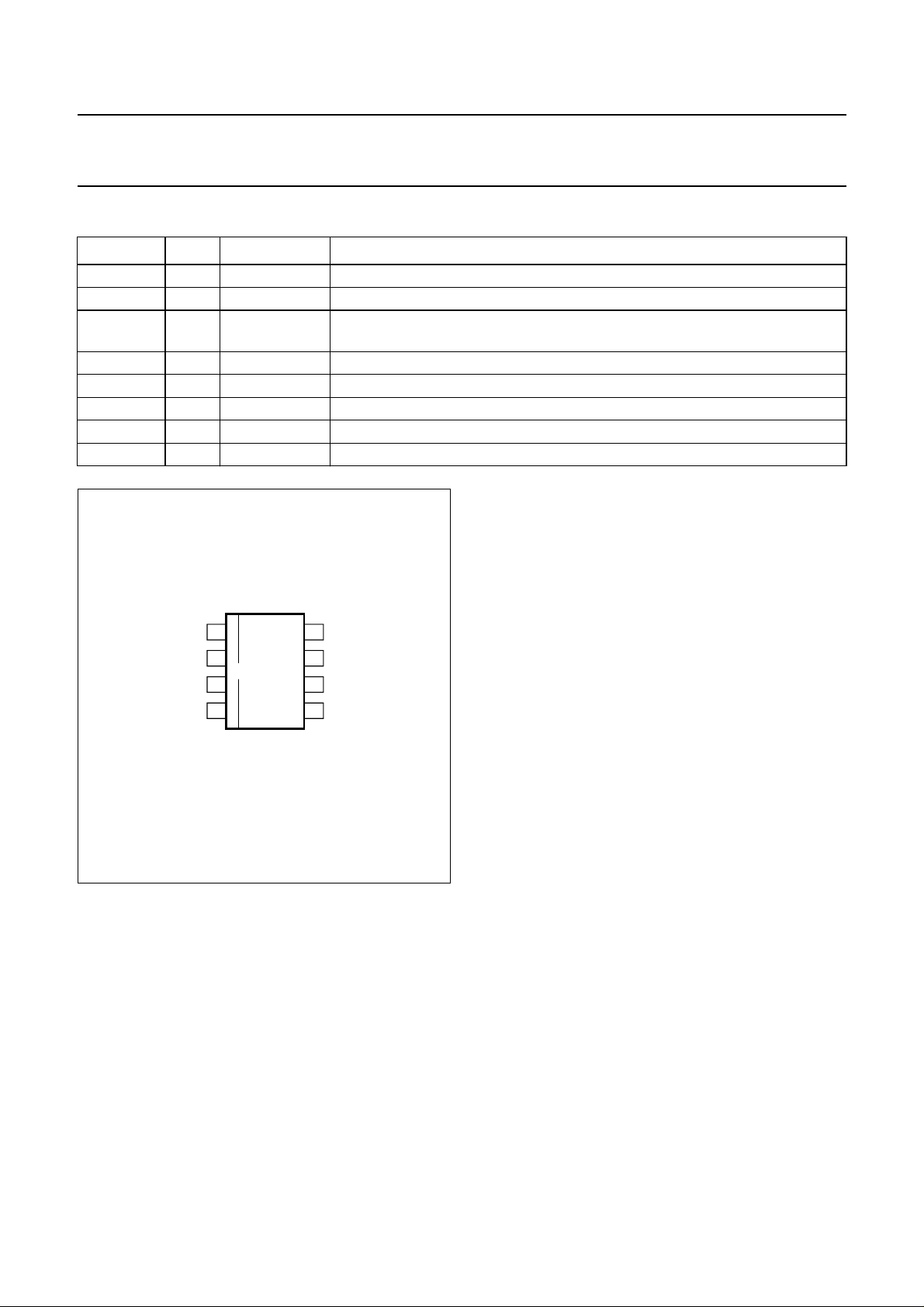
PINNING
SYMBOL PIN TYPE DESCRIPTION
DREF 1 analog output bias voltage for PIN diode (V
GND 2 ground ground
IPhoto 3 analog input current input; anode of PIN diode should be connected to this pin; DC bias
level of 800 mV, one diode voltage above ground
GND 4 ground ground
GND 5 ground ground
OUT 6 CML output data output; OUT goes HIGH when current flows into IPhoto (pin 3)
OUTQ 7 CML output compliment of OUT (pin6)
V
CC
8 supply supply voltage
); cathode should be connected to this pin
CCA
handbook, halfpage
DREF
1
2
TZA3023T
3
IPhoto
4
GND
MGK917
Fig.2 Pin configuration.
V
8
CC
OUTQGND
7
OUT
6
GND
5
1997 Oct 17 3
Philips Semiconductors Objective specification
SDH/SONET STM4/OC12
transimpedance amplifier
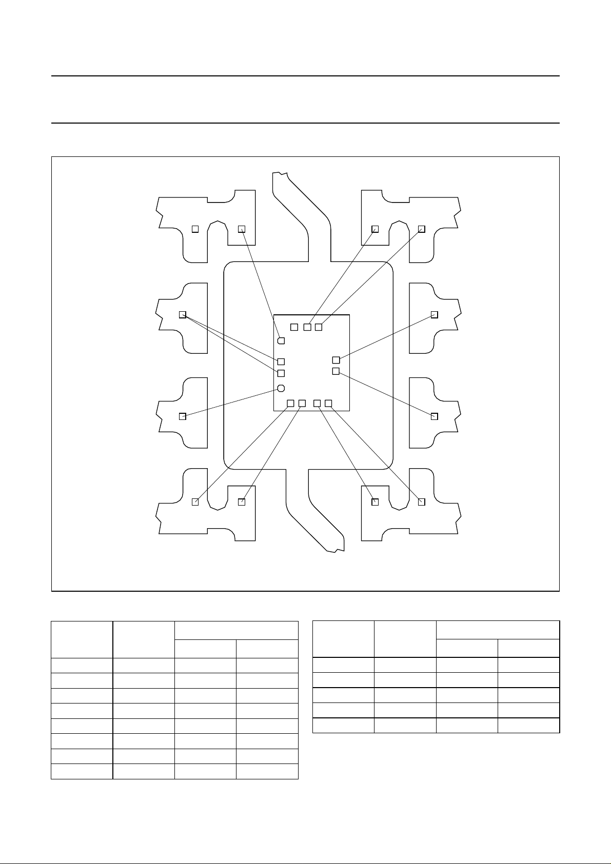
BONDING PAD LOCATIONS
handbook, full pagewidth
DREF
GND
IPhoto
2
36
TZA3023
18
V
CC
AGC
12
13
1
2
TZA3023U
3
4
5
67
11
10
9
8
7
OUTQ
OUT
GND
45
Fig.3 TZA3023U bonding diagram; pad 13 (AGC) is not bonded.
PAD CENTRE LOCATIONS
COORDINATES
(1)
SYMBOL PAD
xy
DREF 1 95 881
GND 2 95 618
GND 3 95 473
IPhoto 4 95 285
GND 5 215 95
GND 6 360 95
GND 7 549 95
GND 8 691 95
1997 Oct 17 4
GND
MGK919
COORDINATES
(1)
SYMBOL PAD
xy
OUT 9 785 501
OUTQ 10 785 641
V
CC
V
CC
11 567 1055
12 424 1055
AGC 13 259 1055
Note
1. All coordinates are referenced, in µm, to the bottom
left-hand corner of the die.
 Loading...