


INTEGRATED CIRCUITS
DATA SH EET
TZA3019
2.5 Gbits/s dual
postamplifier with level
detectors and 2 × 2 switch
Preliminary specification
File under Integrated Circuits, IC19
2000 Apr 10

Philips Semiconductors Preliminary specification
2.5 Gbits/s dual postamplifier with level
detectors and 2 × 2 switch
FEATURES
• Dual postamplifier
• Single 3.3 V power supply
• Wideband operation from 50 kHz to 2.5 GHz (typical
value)
• Fully differential
• Channels are delay matched
• On-chip DC-offset compensations without external
capacitor
• Interfacing with positive or negative supplied logic
• Switching possibility between channels
• PositiveEmitterCoupledLogic(PECL)orCurrent-Mode
Logic (CML) compatible data outputs adjustable from
200 to 800 mV (p-p) single-ended
• Power-downcapability for unused outputs anddetectors
• Rise and fall times 80 ps (typical value)
• Possibility to invert the output of each channel
separately
• Input level-detection circuits for Received Signal
Strength Indicator (RSSI) or Loss Of Signal (LOS)
detection, programmable from 0.4 to 400 mV (p-p)
single-ended, with open-drain comparator output for
direct interfacing with positive or negative logic
• Reference voltage for output level and LOS adjustment
• Automatic strongest input signal switch possibility
(TZA3019 version B)
• HTQFP32 or HBCC32 plastic package with exposed
pad.
TZA3019
APPLICATIONS
• Postamplifier for Synchronous Digital Hierarchy and
Synchronous Optical Network (SDH/SONET)
transponder
• SDH/SONET wavelength converter
• Crosspoint or channel switch
• PECL driver
• Fibre channel arbitrated loop
• Protection ring
• Monitoring
• Signal level detectors
• Swing converter CML 200 mV (p-p) to
PECL 800 mV (p-p)
• Port bypass circuit
• 2.5 GHz clock amplification.
GENERAL DESCRIPTION
The TZA3019 is a low gain postamplifier multiplexer witha
dual RSSI and/or LOS detector that is designed for use in
critical signal path control applications, such as
loop-through, redundant channel switching or Wavelength
Division Multiplexing (WDM). The signal path is
unregistered, so no clock is required for the data inputs.
The signal path is fully differential and delay matched. It is
capable of operating from 50 kHz to 2.5 GHz.
The TZA3019 HTQFP32 and HBCC32 packages can be
delivered in three versions:
• TZA3019AHT and TZA3019AV with two RSSI signals
• TZA3019BHT and TZA3019BV with one RSSI and one
LOS signal
• TZA3019CHT and TZA3019CV with two LOS signals.
ORDERING INFORMATION
TYPE
NUMBER
TZA3019AHT HTQFP32 plastic, heatsink thin quad flat package; 32 leads; body 5 × 5 × 1 mm SOT547-2
TZA3019BHT HTQFP32 plastic, heatsink thin quad flat package; 32 leads; body 5 × 5 × 1 mm SOT547-2
TZA3019CHT HTQFP32 plastic, heatsink thin quad flat package; 32 leads; body 5 × 5 × 1 mm SOT547-2
TZA3019AV HBCC32 plastic, heatsink bottom chip carrier; 32 terminals; body 5 × 5 × 0.65 mm SOT560-1
TZA3019BV HBCC32 plastic, heatsink bottom chip carrier; 32 terminals; body 5 × 5 × 0.65 mm SOT560-1
TZA3019CV HBCC32 plastic,heatsink bottom chip carrier; 32 terminals; body 5 × 5 × 0.65 mm SOT560-1
TZA3019U − bare die; 2.22 × 2.22 × 0.28 mm −
2000 Apr 10 2
NAME DESCRIPTION VERSION
PACKAGE
Philips Semiconductors Preliminary specification
2.5 Gbits/s dual postamplifier with level
detectors and 2 × 2 switch
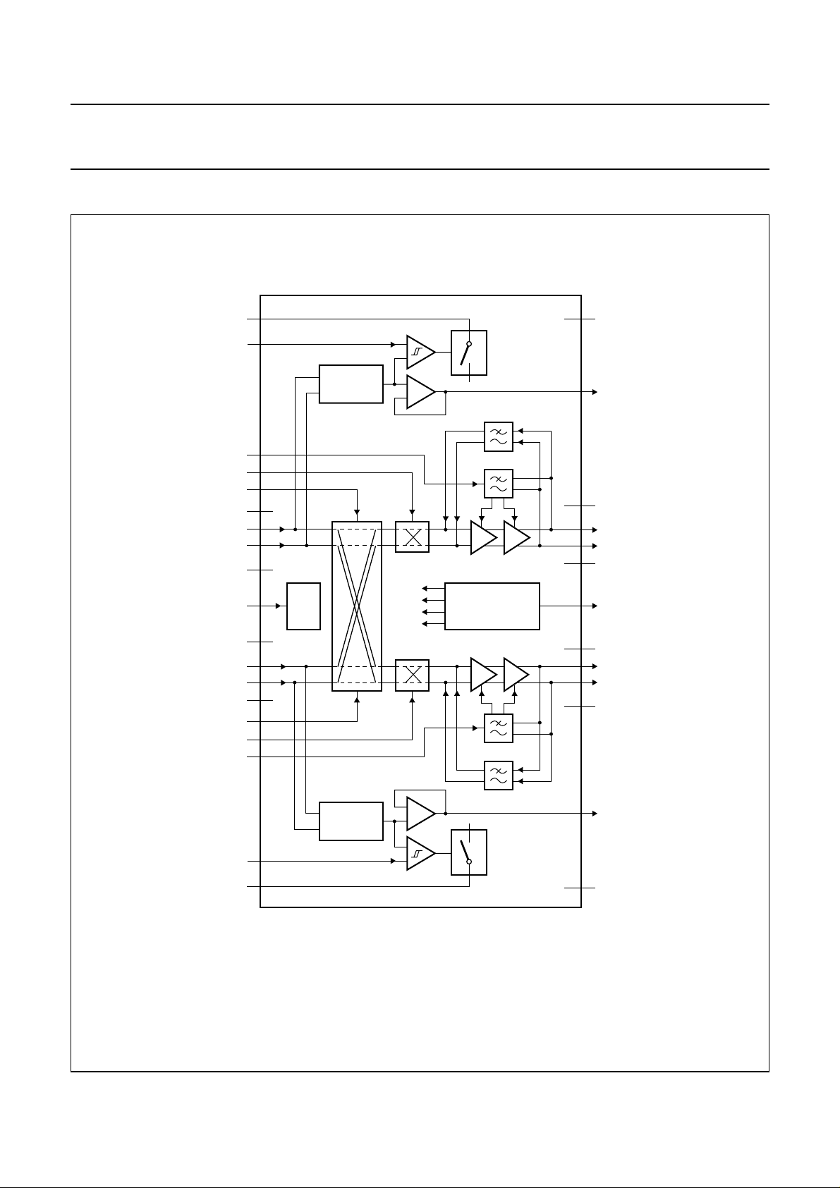
BLOCK DIAGRAM
handbook, full pagewidth
V
EE1A
LOSTH1
LEVEL1
GND1A
IN1Q
GND1A
INV1
S1
IN1
32
10
LOS
DETECTOR
TZA3019AHT
12
29
31
1
2
3
4
TZA3019AV
SWITCH
TZA3019
25
V
EE1B
1×
offset
level
A1A
A1B
27
RSSI1
24
GND1B
23
OUT1
22
OUT1Q
21
GND1B
TEST
GND2A
IN2Q
IN2
GND2A
S2
INV2
LEVEL2
LOSTH2
V
EE2A
15
DFT
8
7
6
5
30
28
13
11
9
SWITCH
LOS
DETECTOR
1×
BAND GAP
REFERENCE
A2B
A2A
level
offset
14
17
18
19
20
26
16
MGT028
V
ref
GND2B
OUT2Q
OUT2
GND2B
RSSI2
V
EE2B
Fig.1 Block diagram (TZA3019AHT and TZA3019AV).
2000 Apr 10 3
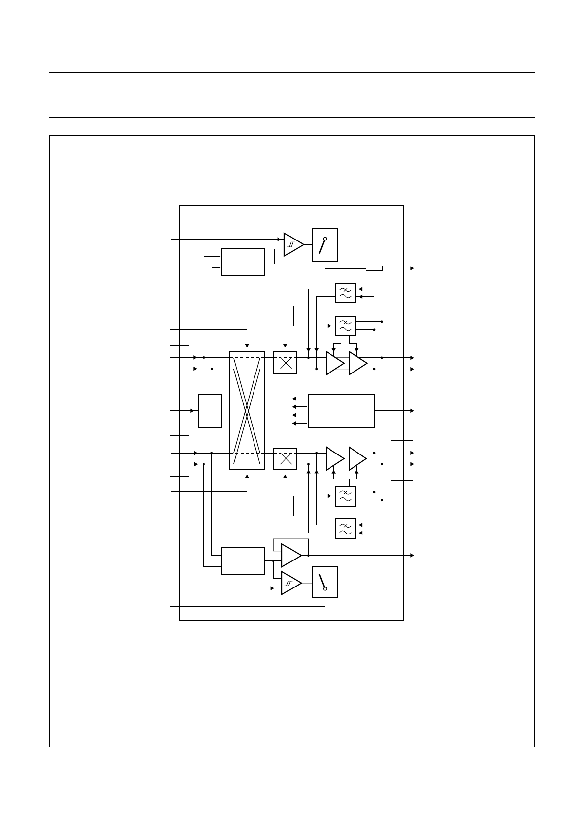
Philips Semiconductors Preliminary specification
2.5 Gbits/s dual postamplifier with level
detectors and 2 × 2 switch
handbook, full pagewidth
V
EE1A
LOSTH1
LEVEL1
GND1A
IN1Q
GND1A
INV1
S1
IN1
32
10
LOS
DETECTOR
TZA3019BHT
12
29
31
1
2
3
4
TZA3019BV
SWITCH
A1A
offset
level
A1B
5 kΩ
TZA3019
25
V
EE1B
27
LOS1
24
GND1B
23
OUT1
22
OUT1Q
21
GND1B
TEST
GND2A
IN2Q
IN2
GND2A
S2
INV2
LEVEL2
LOSTH2
V
EE2A
15
DFT
8
7
6
5
30
28
13
11
9
SWITCH
LOS
DETECTOR
1×
BAND GAP
REFERENCE
A2B
A2A
level
offset
14
17
18
19
20
26
16
MGT027
V
ref
GND2B
OUT2Q
OUT2
GND2B
RSSI2
V
EE2B
Fig.2 Block diagram (TZA3019BHT and TZA3019AV).
2000 Apr 10 4
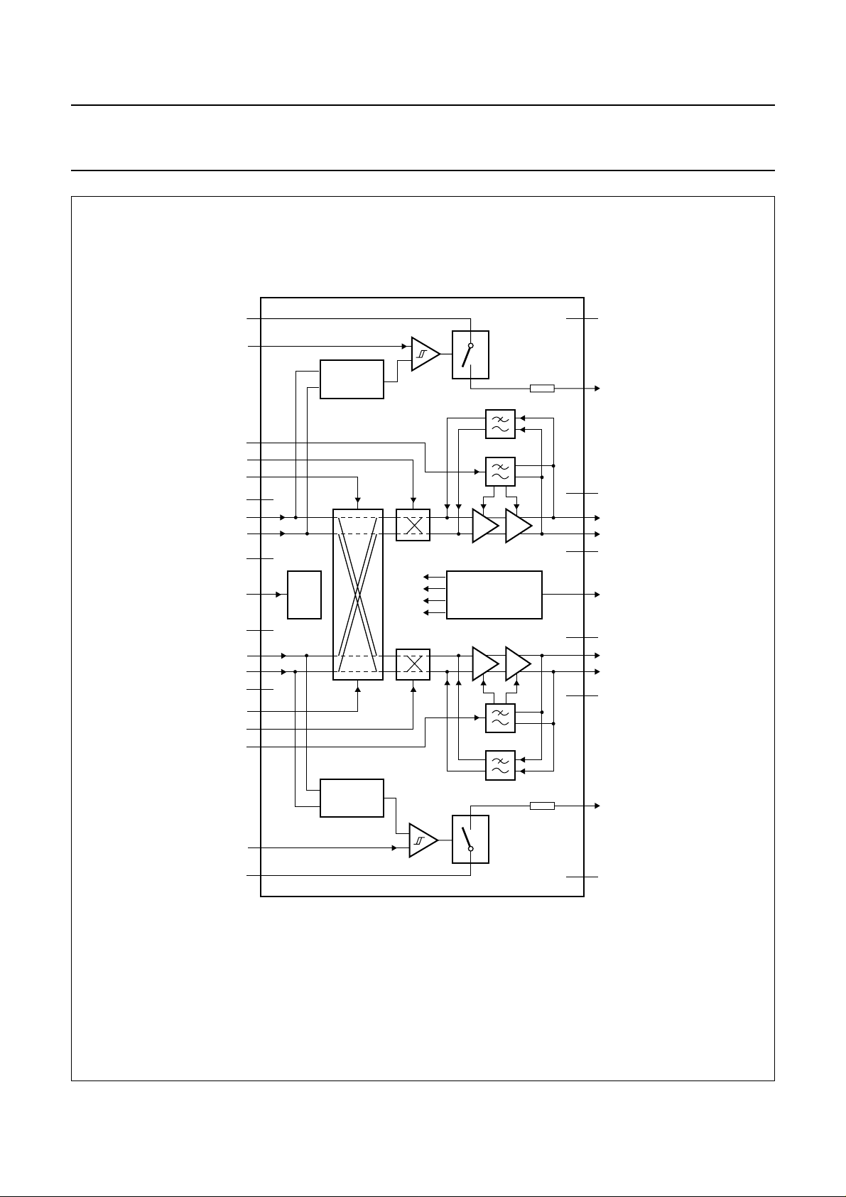
Philips Semiconductors Preliminary specification
2.5 Gbits/s dual postamplifier with level
detectors and 2 × 2 switch
handbook, full pagewidth
V
EE1A
LOSTH1
LEVEL1
GND1A
IN1Q
GND1A
INV1
S1
IN1
32
10
LOS
DETECTOR
TZA3019CHT
12
29
31
1
2
3
4
TZA3019CV
SWITCH
A1A
offset
level
A1B
5 kΩ
TZA3019
25
V
EE1B
27
LOS1
24
GND1B
23
OUT1
22
OUT1Q
21
GND1B
TEST
GND2A
IN2Q
IN2
GND2A
S2
INV2
LEVEL2
LOSTH2
V
EE2A
15
DFT
8
7
6
5
30
28
13
11
9
SWITCH
LOS
DETECTOR
BAND GAP
REFERENCE
A2B
A2A
level
offset
5 kΩ
14
17
18
19
20
26
16
MGS553
V
ref
GND2B
OUT2Q
OUT2
GND2B
LOS2
V
EE2B
Fig.3 Block diagram (TZA3019CHT and TZA3019CV).
2000 Apr 10 5

Philips Semiconductors Preliminary specification
2.5 Gbits/s dual postamplifier with level
TZA3019
detectors and 2 × 2 switch
PINNING
PIN
SYMBOL
(1)
PAD TYPE
ABC
GND1A1111 Sground for input 1 and LOS1 circuits
IN1 2 2 2 2 I differential circuit 1 input; complimentary to pin IN1Q; DC bias level
IN1Q 3 3 3 3 I differential circuit 1 input; complimentary to pin IN1; DC bias level is
GND1A4444 Sground for input 1 and LOS1 circuits
n.c −−−5 −not connected
n.c −−−6 −not connected
GND2A5557 Sground for input 2 and LOS2 circuits
IN2 6 6 6 8 I differential circuit 2 input; complimentary to pin IN2Q; DC bias level
IN2Q 7 7 7 9 I differential circuit 2 input; complimentary to pin IN2; DC bias level is
GND2A88810 Sground for input 2 and LOS2 circuits
V
EE2A
9 9 9 11 S negative supply voltage for input 2 and LOS2 circuits
LOSTH1 10 10 10 12 I Input for level detector programming of input 1 circuit; threshold
LOSTH2 11 11 11 13 I Input for level detector programming of input 2 circuit; threshold
n.c −−−14 − not connected
LEVEL1 12 12 12 15 I Input for programming output level of output 1 circuit; output level is
LEVEL2 13 13 13 16 I Input for programming output level of output 2 circuit; output level is
V
ref
14 14 14 17 O reference voltage for level circuit and LOS threshold programming;
n.c −−−18 −
TEST 15 15 15 19 I for test purposes only; to be left open-circuit in the application
V
EE2B
16 16 16 20 S negative supply voltage for output 2 circuit
GND2B 17 17 17 21 S ground for output 2 circuit
OUT2Q 18 18 18 22 O PECL or CML compatible differential circuit 2 output;
(2)
DESCRIPTIONTZA3019xHT/xV
is set internally at approximately −0.33 V
set internally at approximately −0.33 V
is set internally at approximately −0.33 V
set internally at approximately −0.33 V
level is set by connecting external resistors between pins
GND1A and V
. When forced to V
ref
or not connected, the
EE2A
LOS1 circuit will be switched off.
level is set by connecting external resistors between pins
GND2A and V
. When forced to V
ref
or not connected, the
EE2A
LOS2 circuit will be switched off.
set by connecting external resistors between pins GND1A and V
When forced to GND1A or not connected, pins OUT1 and OUT1Q
will be switched off.
set by connecting external resistors between pins GND2A and V
When forced to GND2A or not connected, pins OUT2 and OUT2Q
will be switched off.
typical value is −1.6 V; no external capacitor allowed
complimentary to pin OUT2
ref
ref
.
.
2000 Apr 10 6

Philips Semiconductors Preliminary specification
2.5 Gbits/s dual postamplifier with level
TZA3019
detectors and 2 × 2 switch
PIN
SYMBOL
ABC
OUT2 19 19 19 23 O PECL or CML compatible differential circuit 2 output;
GND2B 20 20 20 24 S ground for output 2 circuit
n.c −−−25 − not connected
n.c −−−26 − not connected
GND1B 21 21 21 27 S ground for output 1 circuit
OUT1Q 22 22 22 28 O PECL or CML compatible differential circuit 1 output;
OUT1 23 23 23 29 O PECL or CML compatible differential circuit 1 output;
GND1B 24 24 24 30 S ground for output 1 circuit
V
EE1B
RSSI2 26 26 − 32 O output of received signal strength indicator of detector
LOS2 −−26 33 O-DRN output loss of signal detector 2; detection of input 2 signal; direct
RSSI1 27 −−34 O output of received signal strength indicator of detector
LOS1 − 27 27 35 O-DRN output loss of signal detector 2; detection of input 2 signal; direct
INV2 28 28 28 36 TTL input to invert the signal of pins OUT2 and OUT2Q; directly positive
INV1 29 29 29 37 TTL input to invert the signal of pins OUT1 and OUT1Q; directly of
S2 30 30 30 38 TTL input selector output 2 circuit; directly positive (inverted) or negative
S1 31 31 31 39 TTL input selector output 1 circuit; directly positive (inverted) or negative
V
EE1A
V
EEP
Notes
1. The ‘x’ in TZA3019xHT/xV represents versions A, B and C.
2. Pin type abbreviations: O = output, I = input, S = power supply, TTL = logic input and O-DRN = open-drain output.
25 25 25 31 S negative supply voltage for output 1 circuit
32 32 32 40 S negative supply voltage for input 1 and LOS1 circuits
pad pad pad − S negative supply voltage pad (exposed die pad)
(1)
PAD TYPE
(2)
complimentary to pin OUT2Q
complimentary to pin OUT1
complimentary to pin OUT1Q
drive of positive or negative supplied logic via internal 5 kΩ resistor
drive of positive or negative supplied logic via internal 5 kΩ resistor
(inverted) or negative supplied logic driven
positive (inverted) or negative supplied logic driven
supplied logic driven
supplied logic driven
DESCRIPTIONTZA3019xHT/xV
2000 Apr 10 7
Philips Semiconductors Preliminary specification
2.5 Gbits/s dual postamplifier with level
detectors and 2 × 2 switch
handbook, full pagewidth
EE1A
V
S1
S2
31
GND1A
IN1
IN1Q
GND1A
GND2A
IN2
IN2Q
GND2A
32
1
2
3
4
5
6
7
8
9
EE2A
V
30
exposed pad
TZA3019xHT
11
10
LOSTH2
LOSTH1
INV1
29
12
LEVEL1
INV2
RSSI1/LOS1
28
27
V
13
14
V
LEVEL2
RSSI2/LOS2
26
EEP
15
ref
TEST
EE1B
V
25
16
EE2B
V
24
23
22
21
20
19
18
17
MGS554
TZA3019
GND1B
OUT1
OUT1Q
GND1B
GND2B
OUT2
OUT2Q
GND2B
handbook, full pagewidth
GND1A
IN1
IN1Q
GND1A
GND2A
IN2
IN2Q
GND2A
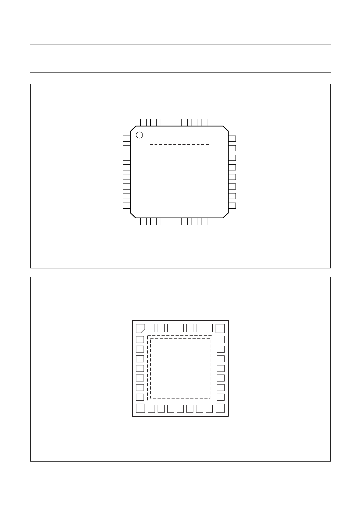
Fig.4 Pin configuration HTQFP32.
EE1A
S1
V
1 3231302928272625
2
3
4
5
6
7
8
9
10 11 12 13 14 15
EE2A
V
LOSTH1
S2
exposed pad
TZA3019xV
LEVEL1
LOSTH2
INV1
LEVEL2
INV2
ref
V
V
EEP
RSSI1/LOS1
RSSI2/LOS2
24
23
22
21
20
19
18
17
16
TEST
EE2B
V
EE1B
V
GND1B
OUT1
OUT1Q
GND1B
GND2B
OUT2
OUT2Q
GND2B
MGT029
Fig.5 Pin configuration HBCC32.
2000 Apr 10 8
Philips Semiconductors Preliminary specification
2.5 Gbits/s dual postamplifier with level
detectors and 2 × 2 switch
FUNCTIONAL DESCRIPTION
The TZA3019 is a dual postamplifier with multiplexer and
loss of signal detection see Figs 1, 2 and 3. The RF path
starts with the multiplexer, which connects an amplifier to
one of the two inputs. It is possible to invert the output for
easy layout of the Printed-Circuit Board (PCB). The signal
is amplified to a certain level. To guarantee this level with
minimum distortion over the temperature range and level
range, an active control part is added. The offset
compensation circuit following the inverter minimizes the
offset.
TheReceivedSignal Strength Indicator (RSSI) or the Loss
Of Signal (LOS) detection uses a 7-stage ‘successive
detection’circuit.It provides a logarithmic output. The LOS
is followed by a comparator with a programmable
threshold. The input signal level-detection is implemented
to check if the input signal voltage is above the user
programmed level. This can insure that data will only be
transmittedwhentheinputsignal-to-noiseratio is sufficient
for low bit error rate system operation. A second
offset compensation circuit minimizes the offset of the
logarithmic amplifier.
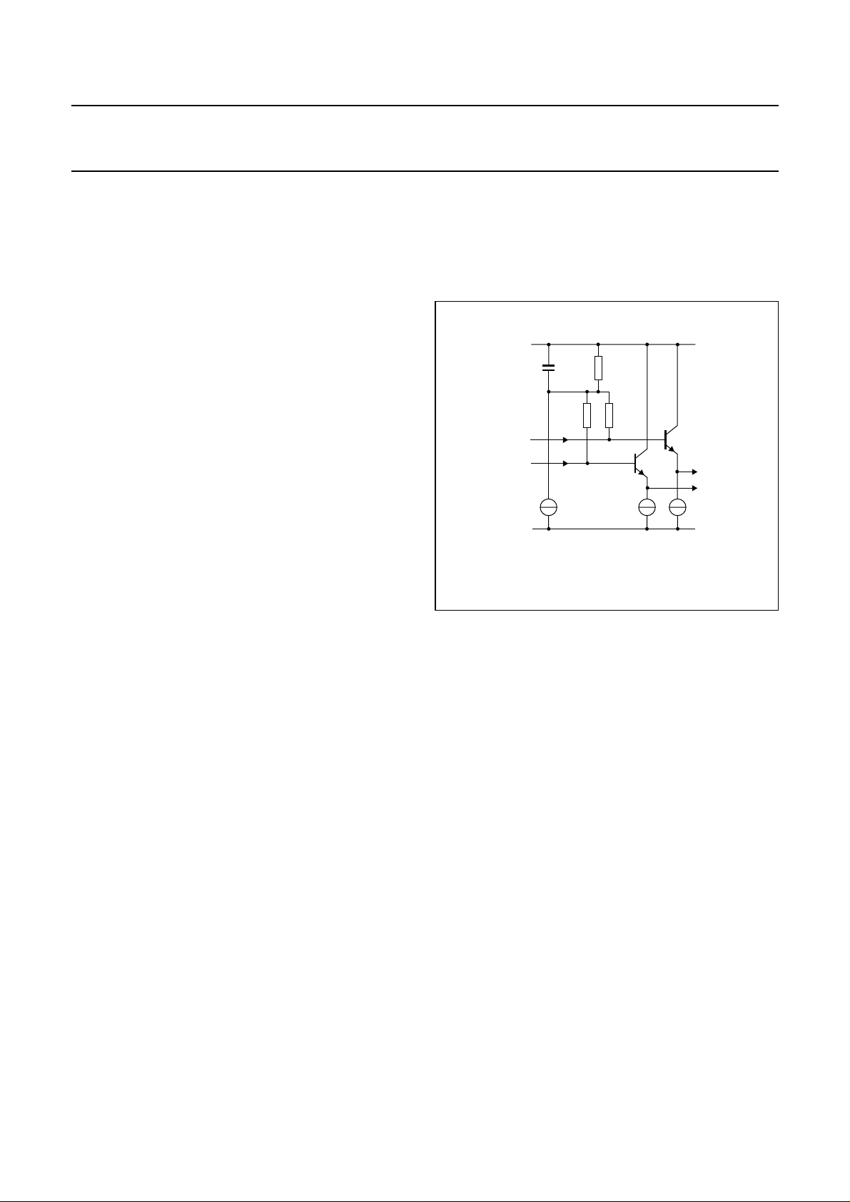
RF input circuit
TZA3019
In such cases, pull-up resistors of 100 Ω should be
connected as close as possible to the IC from
pins OUT1 and OUT1Q, and pins OUT2 and OUT2Q to
V
and V
EE1B
are not needed in most applications.
handbook, halfpage
IN1, IN2
IN1Q, IN2Q
respectively. These matching resistors
EE2B
GND1A,
GND2A
12 pF
420 Ω
50 Ω50 Ω
MGS555
V
V
Fig.6 RF input circuit.
EE1A
EE2A
,
The input circuit contains internal 50 Ω resistors
decoupled to ground via an internal common mode 12 pF
capacitor (see Fig.6).
The input pins are DC-biased at approximately −0.33 V by
an internal reference generator. The TZA3019 can be
DC-coupled, but AC-coupling is preferred. In case of
DC-coupling, the driving source must operate within the
allowableinputrange(−1.0 to +0.3 V). A DC-offset voltage
of more than a few millivolts should be avoided, since the
internal DC-offset compensation circuit has a limited
correction range. When AC-coupling is used, if no
DC-compatibility is required, the values of the coupling
capacitors must be large enough to pass the lowest input
frequency of interest. Capacitor tolerance and resistor
variation must be included for an accurate calculation.
Do not use signal frequencies around the low cut-off
circuit frequencies (f
and f
= 1 MHz for the LOS circuits).
−3dB(l)
= 50 kHz for the postamplifiers
−3dB(l)
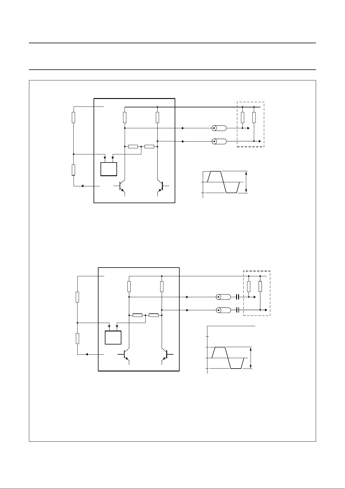
RF output circuit
Matching the main amplifier outputs (see Fig.7) is not
mandatory. In most applications, the transmission line
receiving end will be properly matched, while very little
reflections occur.
Matching the transmitting end to absorb reflections is only
recommended for very sensitive applications.
Postamplifier level adjustment
Thepostamplifier boosts the signal up to PECL levels. The
output can be either CML- or PECL-level compatible,
adjusted by means of the voltage on pins LEVEL1
and LEVEL2.TheDC voltagesofpins OUT1 and OUT1Q,
and pins OUT2 and OUT2Q match with the DC-levels
on pins LEVEL1 and LEVEL2, respectively. Due to the
receiving end 50 Ω load resistance, it means that at the
same level of V
AC-coupling are not equal to V
o(p-p)
, V
LEVEL1
and V
LEVEL1
LEVEL2
and V
with
LEVEL2
with
DC-coupling (see Figs 7 and 8).
The postamplifier is in power-down state when pin
LEVEL1 or LEVEL2 is connected to ground or not
connected (see Fig.8).
Postamplifier DC offset cancellation loop
Offset control loops connected between the inputs of the
buffersA1Aand A2A and the outputs of the amplifiers A1B
and A2B (see Figs 1, 2 and 3) will keep the input of both
buffers at their toggle point during the absence of an input
signal.Theactiveoffset compensation circuit is integrated,
so no external capacitor is required. The loop time
constant determines the lower cut-off frequency of the
amplifier chain. The cut-off frequency of the offset
compensations is fixed internally at approximately 5 kHz.
2000 Apr 10 9
Philips Semiconductors Preliminary specification
2.5 Gbits/s dual postamplifier with level
detectors and 2 × 2 switch
o(se)(p-p)
×=
---------------------R1 R2+
GND1A,
GND2A
R1
LEVEL1,
LEVEL2
R2
.
R1
V
100 Ω
level
100 Ω
REG
V
ref
.
LEVEL1
or V
LEVEL2=VGND
.
handbook, full pagewidth
V
= 0.5 × V
level
V
levelVref
Level detector in power-down mode: V
GND1B,
GND2B
OUT1,
OUT2
OUT1Q,
OUT2Q
V
level
V
o
(V)
TZA3019
50
50
Ω
V
o
0
Ω
V
o(se)(p-p)
MGS556
handbook, full pagewidth
GND1A,
GND2A
R1
LEVEL1,
LEVEL2
R2
V
ref
V
= 1.5 × V
level
V
levelVref
Level detector in power-down mode: V
o(se)(p-p)
×=
---------------------R1 R2+
R1
.
.
V
level
REG
LEVEL1
100 Ω
or V
LEVEL2=VGND
a. DC-coupling.
GND1B,
GND2B
100 Ω
OUT1,
OUT2
OUT1Q,
OUT2Q
.
V
level
V
o
(V)
50
50
Ω
V
o
Ω
0
V
o(se)(p-p)
MGL811
b. AC-coupling.
Fig.7 RF output configurations.
2000 Apr 10 10
 Loading...