

Philips TZA3014VH, TZA3014HT, TZA3014U Datasheet

INTEGRATED CIRCUITS
DATA SH EET
TZA3014
2.5 Gbits/s postamplifier with level
detector
Product specification
Supersedes data of 2000 Aug 09
File under Integrated Circuits, IC19
2001 Jun 25
Philips Semiconductors Product specification
2.5 Gbits/s postamplifier with level detector TZA3014
FEATURES
• Single 3.3 V power supply
• Wideband operation from 50 kHz to 2.5 GHz (typical
value)
• Fully differential
• On-chip DC-offset compensation without external
capacitor
• Interfacing with supplied positive or negative logic
• PositiveEmitterCoupledLogic (PECL)orCurrent-Mode
Logic (CML) compatible data outputs adjustable from
200 to 800 mV (p-p) single-ended
• Power-down capability for unused output or detector
• Rise and fall times of 80 ps (typical value)
• Inverted output possible
• Inputlevel detection circuit forReceived Signal Strength
Indicator (RSSI) and Loss Of Signal (LOS),
programmable from 0.4 to 400 mV (p-p) single-ended,
with open-drain comparator output for directly
interfacing positive or negative logic
• Reference voltage for output level and LOS adjustment
• HTQFP32 and HBCC32 plastic packages with exposed
pad
• Mute input.
APPLICATIONS
• Postamplifier for SDH/SONET transponder
• SDH/SONET wavelength converter
• PECL driver
• Fibre channel arbitrated loop
• Signal level detectors
• Swing converter CML 200 mV (p-p) to
PECL 800 mV (p-p)
• 2.5 GHz clock amplification.
GENERAL DESCRIPTION
The TZA3014 is a low gain postamplifier with a LOS
detectorand a RSSIdesigned for use in critical signal path
control applications, such as loop-through or Wavelength
DivisionMultiplexing (WDM). The signalpath is capable of
operating from 50 kHz up to 2.5 GHz.
The TZA3014 canbe delivered in HTQFP32 andHBCC32
packages and as bare die.
ORDERING INFORMATION
TYPE
NUMBER
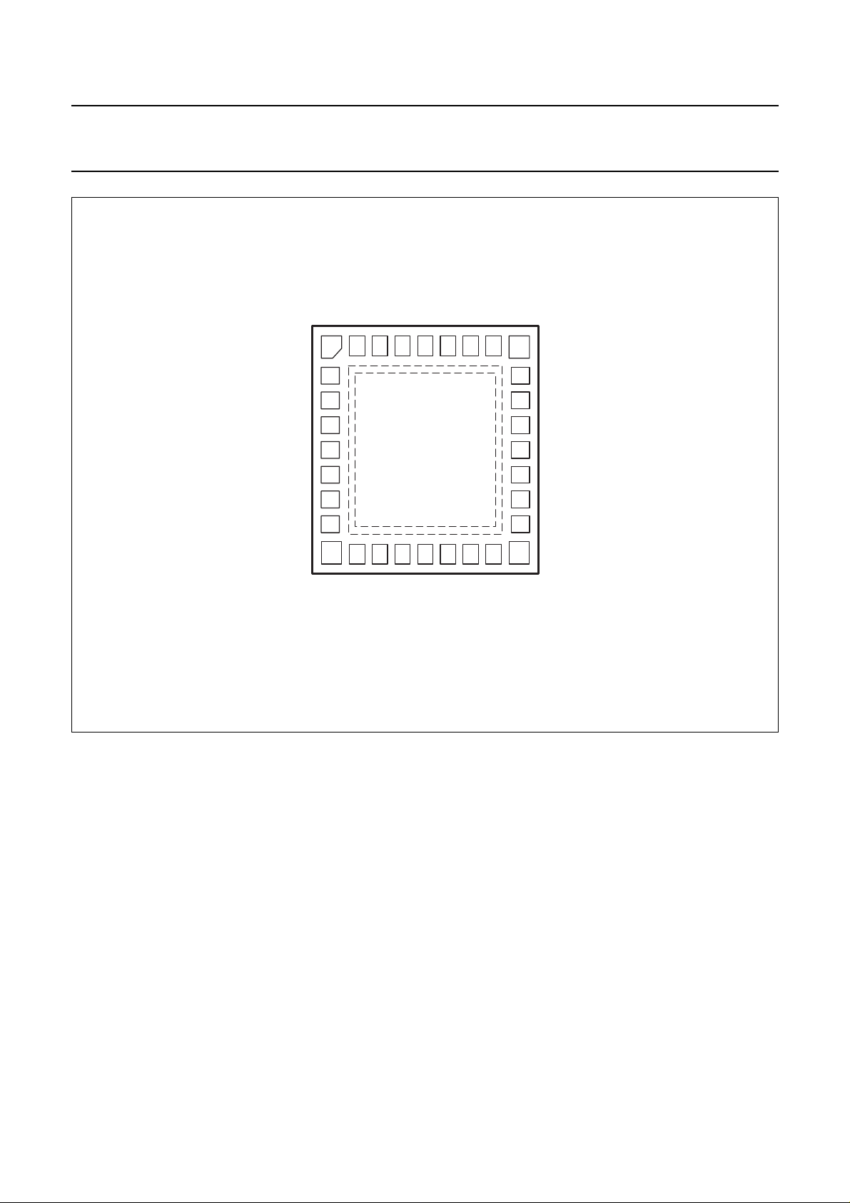
TZA3014HT HTQFP32 plastic, heatsink thin quad flat package; 32 leads; body 5 × 5 × 1.0 mm SOT547-2
TZA3014VH HBCC32 plastic, heatsink bottom chip carrier; 32 terminals; body 5 × 5 × 0.65 mm SOT560-1
TZA3014U − bare die; 2.22 × 2.22 × 0.28 mm −
NAME DESCRIPTION VERSION
PACKAGE
2001 Jun 25 2
Philips Semiconductors Product specification
2.5 Gbits/s postamplifier with level detector TZA3014
BLOCK DIAGRAM
handbook, full pagewidth
GNDA
LOSTH
LEVEL
INV
V
CCA
INQ
V
CCA
TEST
MUTE
32 (40)
10 (12)
12 (15)
29 (37)
1
2
IN
3
4
15 (19)
31 (39)
disable LOS output
RSSI
TZA3014
comparator
1×
cross-over
switch
offset compensationoffset compensation
level
buffer
BAND GAP
REFERENCE
5 kΩ
amplifier
(31) 25
(35) 27
(34) 26
(30) 24
(29) 23
(28) 22
(27) 21
(17) 14
MGU122
GNDB
LOS
RSSI
V
CCB
OUT
OUTQ
V
CCB
V
ref
The numbers in parentheses refer to the pad numbers of the bare die version.
Fig.1 Block diagram.
2001 Jun 25 3
Philips Semiconductors Product specification
2.5 Gbits/s postamplifier with level detector TZA3014
PINNING
SYMBOL PIN PAD TYPE
V
CCA
1 1 S supply voltage for input and LOS detector
(1)
DESCRIPTION
IN 2 2 I differential input; complimentary to pin INQ; DC bias level is set internally
at approximately V
− 0.33 V
CC
INQ 3 3 I differential input; complimentary to pin IN; DC bias level is set internally at
V
CCA
approximately V
4 4 S supply voltage for input and LOS detector
− 0.33 V
CC
n.c. − 5 − not connected
n.c. − 6 − not connected
n.c. 5 7 − not connected
n.c. 6 8 I not connected
n.c. 7 9 I not connected
n.c. 8 10 S not connected
n.c. 9 11 S not connected
LOSTH 10 12 I input for setting threshold level of LOS detector; threshold level is set by
connecting external resistors between pins V
CCA
and V
; when forced to
ref
GNDA or not connected, the LOS detector is switched off
n.c. 11 13 I not connected
n.c. − 14 − not connected
LEVEL 12 15 I input for setting AC level of the output circuit; output signal level is set by
connecting external resistors between pins V
V
or not connected, pins OUT and OUTQ will be switched off
CCA
CCA
and V
; when forced to
ref
n.c. 13 16 I not connected
V
ref
14 17 O reference voltage for programming output level circuit and LOS threshold;
typical value is VCC− 1.6 V; no external capacitor allowed
n.c. − 18 − not connected
TEST 15 19 I for test purposes only; to be left open-circuit in the application
n.c. 16 20 S not connected
n.c. 17 21 S not connected
n.c. 18 22 O not connected
n.c. 19 23 O not connected
n.c. 20 24 S not connected
n.c. − 25 − not connected
n.c. − 26 − not connected
V
CCB
21 27 S supply voltage for output circuit
OUTQ 22 28 O PECL or CML compatible differential output; complimentary to pin OUT
OUT 23 29 O PECL or CML compatible differential output; complimentary to pin OUTQ
V
CCB
24 30 S supply voltage for output circuit
GNDB 25 31 S ground for output circuit
n.c. − 32 O not connected
n.c. − 33 O-DRN not connected
2001 Jun 25 4
Philips Semiconductors Product specification
2.5 Gbits/s postamplifier with level detector TZA3014
SYMBOL PIN PAD TYPE
(1)
DESCRIPTION
RSSI 26 34 O RSSI output
LOS 27 35 O-DRN output of LOS detector; direct drive to either positive or negative supplied
logic via internal 5 kΩ resistor
n.c. 28 36 TTL not connected
INV 29 37 TTL input to invert the signal at pins OUT and OUTQ; supports positive or
negative logic
n.c. 30 38 TTL not connected
MUTE 31 39 TTL input to mute the output signal on pins OUT (‘0’) and OUTQ (‘1’); supports
positive or negative logic
GNDA 32 40 S ground for input and LOS detector
GNDp pad − S ground pad (exposed die pad)
Note
1. Pin type abbreviations: O = output, I = input, S = power supply, TTL = logic input and O-DRN = open-drain output.
handbook, full pagewidth
GNDA
32
MUTE
31
n.c.
30
INV
29
n.c.
28
LOS
27
RSSI
26
GNDB
25
1
V
CCA
2
V
INQ
CCA
n.c.
n.c.
n.c.
n.c.
IN
3
4
5
6
7
8
9
n.c.
exposed pad
TZA3014HT
11
10
n.c.
LOSTH
12
LEVEL
13
n.c.
GNDp
14
ref
V
Fig.2 Pin configuration HTQFP32 package.
15
TEST
16
n.c.
24
23
22
21
20
19
18
17
MGU123
V
CCB
OUT
OUTQ
V
CCB
n.c.
n.c.
n.c.
n.c.
2001 Jun 25 5
Philips Semiconductors Product specification
2.5 Gbits/s postamplifier with level detector TZA3014
handbook, full pagewidth
GNDA
MUTE
n.c.
INV
n.c.
LOS
RSSI
GNDB
V
V
CCA
CCA
1 3231302928272625
IN
INQ
2
3
exposed pad
4
n.c.
n.c.
n.c.
n.c.
5
6
7
8
9
n.c.
TZA3014VH
10 11 12 13 14 15
n.c.
LOSTH
n.c.
LEVEL
GNDp
ref
V
16
TEST
n.c.
Fig.3 Pin configuration HBCC32 package.
24
23
22
21
20
19
18
17
V
CCB
OUT
OUTQ
V
CCB
n.c.
n.c.
n.c.
n.c.
MGU124
2001 Jun 25 6
Philips Semiconductors Product specification
2.5 Gbits/s postamplifier with level detector TZA3014
FUNCTIONAL DESCRIPTION
The TZA3014 is a postamplifier with a RSSI circuit to
provide output signals for RSSI and LOS (see Fig.1). The
input signal can be amplified to a programmable level.
An active level control circuit ensures this level. The
control voltage on pin INV inverts the outputs, so avoiding
arequiredcomplicatedPrintedCircuit Board (PCB) layout.
An offset compensation circuit minimizes the effect of any
voltage offset present at the input.
The RSSI and LOS detector are based on a 7-stage
‘successive detection’ circuit which provides a logarithmic
output. The LOS detector is followed bya comparator with
aprogrammablethreshold.Theinputsignalleveldetection
is implemented to check if the input signal is above the
user-programmedlevel. The usercan ensure that datawill
only be transmitted when the input signal-to-noise ratio is
sufficient for low bit error rate system operation. A second
offset compensation circuit minimizes the effect of any
voltage offset present in the logarithmic amplifier.
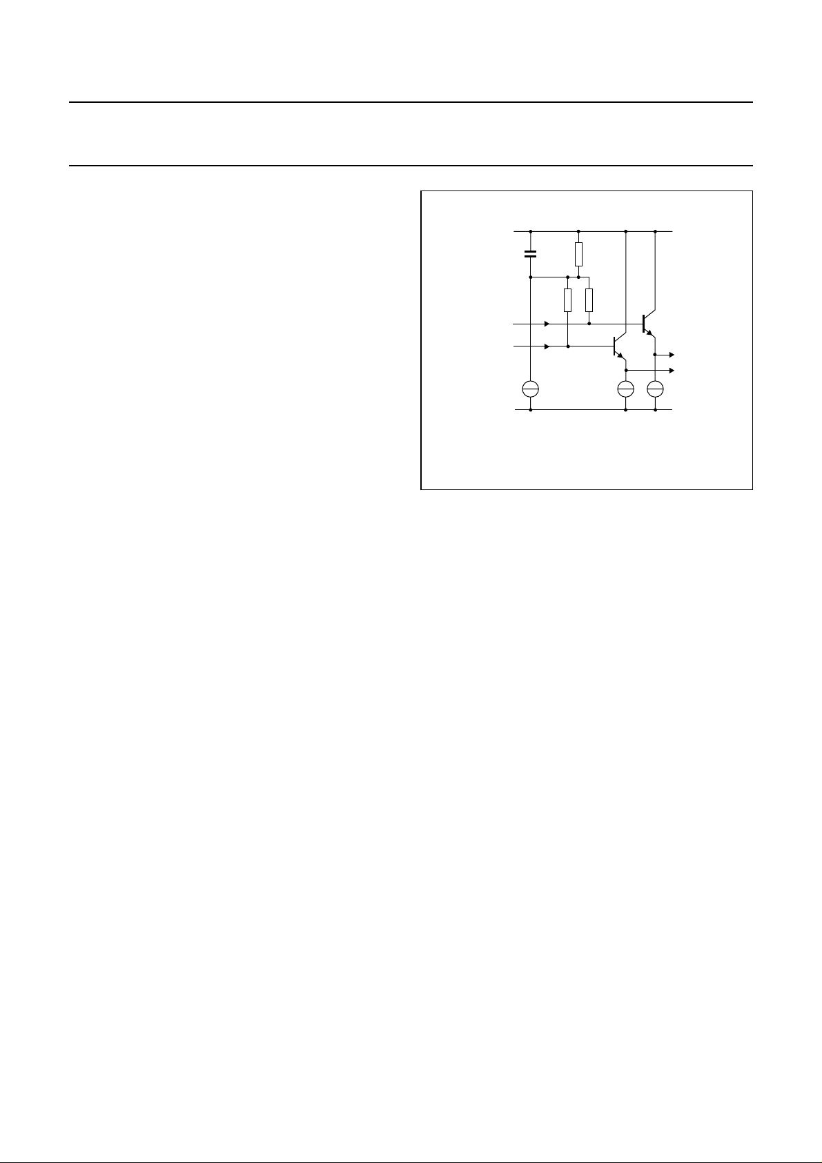
RF input circuit
The input circuit contains internal 50 Ω resistors
decoupled to V
via an internal common mode 12 pF
CCA
capacitor (see Fig.4).
The inputs IN and INQ are DC-biased at approximately
V
− 0.33 V by an internal reference generator. The
CCA
TZA3014 can be DC-coupled, but AC coupling is
preferred. When DC-coupled, the drive source must
operate within the allowable input range
(V
− 1.0 V to V
CCA
+ 0.3 V). The DC-offset voltage
CCA
should stay below a few millivolts since the internal
DC-offset compensation circuit has a limited correction
range. When AC-coupled, do not use capacitors that
cause a 3 dB cut-off point at 50 kHz (postamplifier cut-off
point) or at 1 MHz (RSSI cut-off point).
RF output circuit
Matching the outputs of the postamplifier (seeFig.5) is not
mandatory. In most applications, the receiving end of the
transmission line will be properly matched, causing very
few reflections.
Matching the transmitting end of the transmission line to
absorb reflections only, is recommended for verysensitive
applications.
handbook, halfpage
IN
INQ
12 pF
420 Ω
50 Ω50 Ω
V
CCA
GNDA
MGU125
Fig.4 RF input circuit.
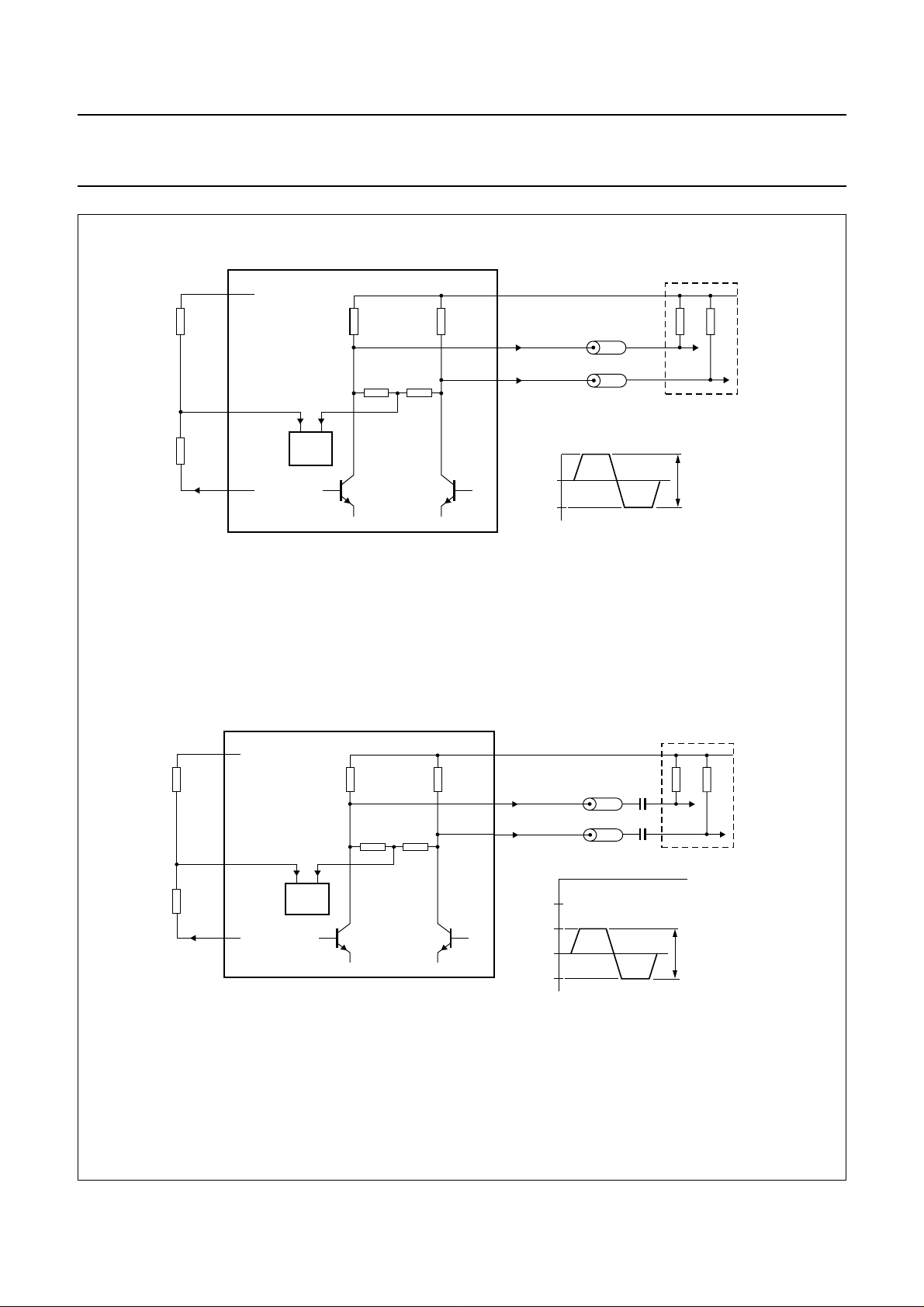
RF output level adjustment
The output level can be made compatible with CML or
PECL by adjusting the voltage on pin LEVEL. The
DC voltages on pins OUT and OUTQ relate to the
DC voltage on pin LEVEL. Due to the effect of the 50 Ω
load resistance at the receiving end, for a given
peak-to-peak value on pins OUT and OUTQ, a different
voltage is required on pin LEVEL in case the output is
AC-coupled and when the output is DC-coupled
(see Figs 5 and 6).
When pin LEVEL is not connected or connected to V
CCA
the postamplifier is in power-down state (see Fig.5).
DC-offset compensation loop
A DC-offset compensation loop connected between the
amplifier output and the buffer input maintains the toggle
point at the buffer input when there is no input signal
(see Fig.1). This active control circuit is integrated and
does not require an external capacitor. The loop
time constant determines the lower cut-off frequency of
the amplifier chain, and is internally fixed at approximately
5 kHz.
,
In such cases, 100 Ω pull-up resistors should be
connected to V
and pins OUT and OUTQ as close as
CCB
possible to the IC. However, for most applications these
matching resistors are not required.
2001 Jun 25 7
Philips Semiconductors Product specification
2.5 Gbits/s postamplifier with level detector TZA3014
handbook, full pagewidth
V
= 0.5 × V
LEVEL
V
LEVELVref
V
LEVEL=VCC
V
4
CCA
R1
12 (15)
LEVEL
R2
V
14 (17)
ref
.
o(se)(p-p)
R1
×=
---------------------R1 R2+
for power-down mode.
V
LEVEL
100 Ω
REG
The numbers in parentheses refer to the pad numbers of the bare die version.
a. DC-coupled.
(27) 21
100 Ω
(29) 23
(28) 22
V
CCB
OUT
OUTQ
V
V
CC
LEVEL
V
o
(V)
V
o
Transmission
lines
50
Ω
V
o(se)(p-p)
MGU126
50
Ω
handbook, full pagewidth
V
= 1.5 × V
LEVEL
V
LEVELVref
V
LEVEL=VCC
V
CCA
4
R1
12 (15)
LEVEL
R2
V
14 (17)
ref
.
o(se)(p-p)
R1
×=
---------------------R1 R2+
for power-down mode.
V
LEVEL
100 Ω
REG
The numbers in parentheses refer to the pad numbers of the bare die version.
b. AC-coupled.
Fig.5 RF output configurations.
(27) 21
100 Ω
(29) 23
(28) 22
V
CCB
OUT
OUTQ
V
V
CC
LEVEL
V
o
(V)
V
o
Transmission
lines
50
Ω
V
o(se)(p-p)
MGU127
50
Ω
2001 Jun 25 8
Philips Semiconductors Product specification
2.5 Gbits/s postamplifier with level detector TZA3014
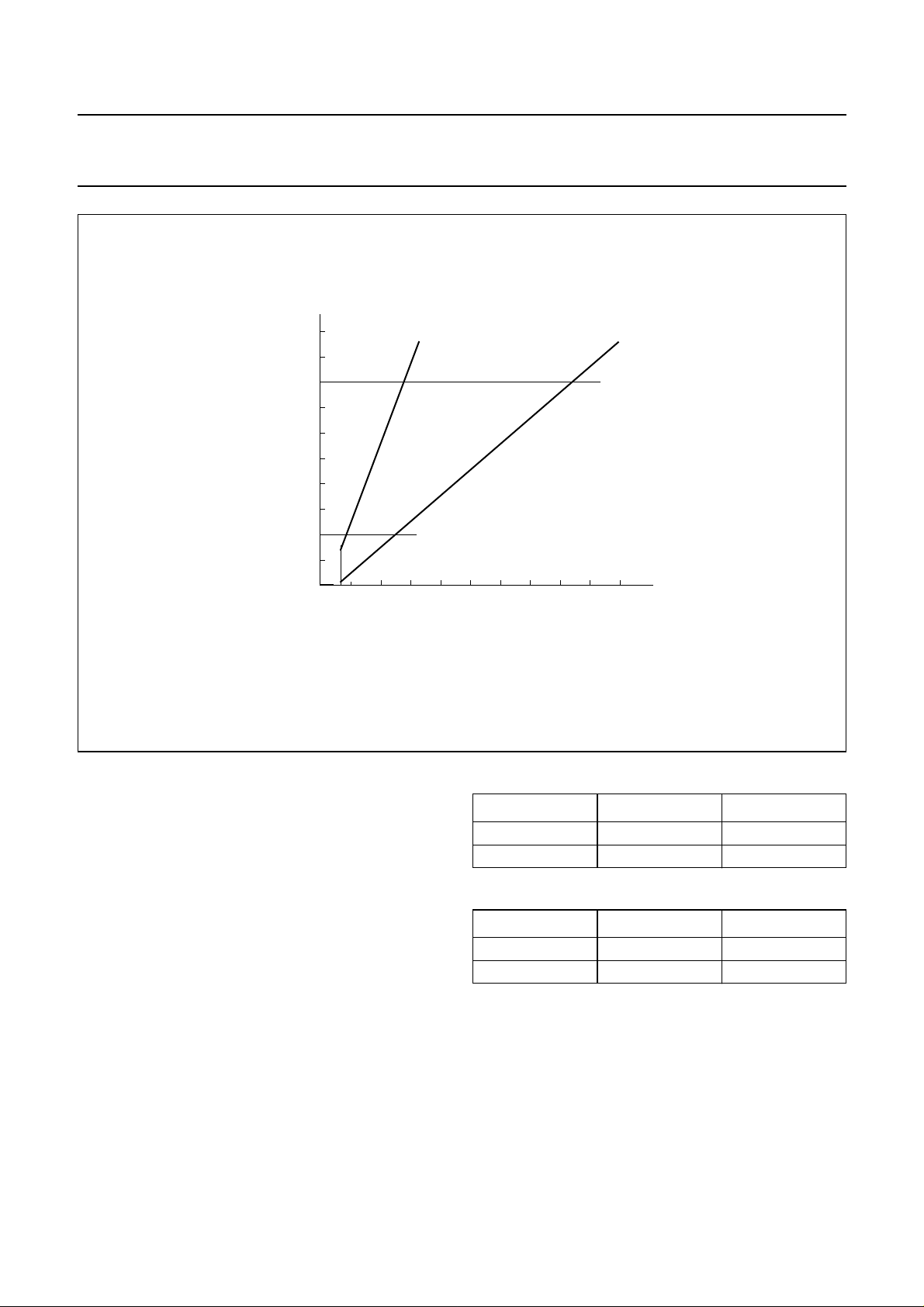
handbook, full pagewidth
V
o(se)(p-p)
(mV)
1000
800
DC-coupled AC-coupled
600
400
200
0
0 100
20 40 60 80
V
LEVEL
Fig.6 Output signal as a function of V
(% of V
LEVEL
MGU128
)
ref
.
TTL logic inputs MUTE and INV
It should be noted that switch control voltages in positive
logicare inverted in case anegativesupply voltage is used
(see Fig.7).
Output signal as a function of inputs MUTE and INV
The default logic level for inputs MUTE and INV is 0 in
case these pins are not connected. See Tables 1 and 2.
2001 Jun 25 9
Table 1 OUT and OUTQ as a function of input MUTE
MUTE OUT OUTQ
0 IN INQ
1 ‘0’ ‘1’
Table 2 OUT and OUTQ as a function of input INV
INV OUT OUTQ
0 IN INQ
1 INQ IN
 Loading...