

Philips tza3013a, tza3013b DATASHEETS

INTEGRATED CIRCUITS
DATA SH EET
TZA3013A; TZA3013B
SDH/SONET STM16/OC48
transimpedance amplifier
Objective specification
File under Integrated Circuits, IC19
2000 Jun 19
Philips Semiconductors Objective specification
SDH/SONET STM16/OC48
TZA3013A; TZA3013B
transimpedance amplifier
FEATURES
• Low equivalent input noise, typically 8 pA/√Hz
• Wide dynamic range, typically 6 µA to 1.7 mA (p-p)
• Differential transimpedance of 4 kΩ
• Bandwidth from DC to 1.9 GHz
• Differential outputs
• On-chip Automatic Gain Control (AGC)
• No external components required
• Single supply voltage 3.3 V
• Bias voltage for PIN diode
• Remains linear up to 1.7 mA (p-p) input current
(unclipped)
• Switched output polarity available (types A and B).
ORDERING INFORMATION
TYPE
NUMBER
TZA3013AHL LQFP32 plastic low profile quad flat package; 32 leads; body 5 × 5 × 1.4 mm SOT401-1
TZA3013AU − bare die in waffle pack carriers; die dimensions 0.810 × 1.230 mm −
TZA3013BU − bare die in waffle pack carriers; die dimensions 0.810 × 1.230 mm −
NAME DESCRIPTION VERSION
APPLICATIONS
• Digital fibre optic receiver in short, medium and long
haul optical telecommunications transmission systems
or in high speed data networks
• Wide-band RF gain block.
GENERAL DESCRIPTION
The TZA3013 is a transimpedance amplifier with AGC,
designed to be used in STM16/OC48 fibre-optic links.
It amplifies the current generated by a photo detector
(PIN diode or avalanche photodiode) and converts it to a
differential output voltage.
PACKAGE
2000 Jun 19 2
Philips Semiconductors Objective specification
SDH/SONET STM16/OC48
transimpedance amplifier
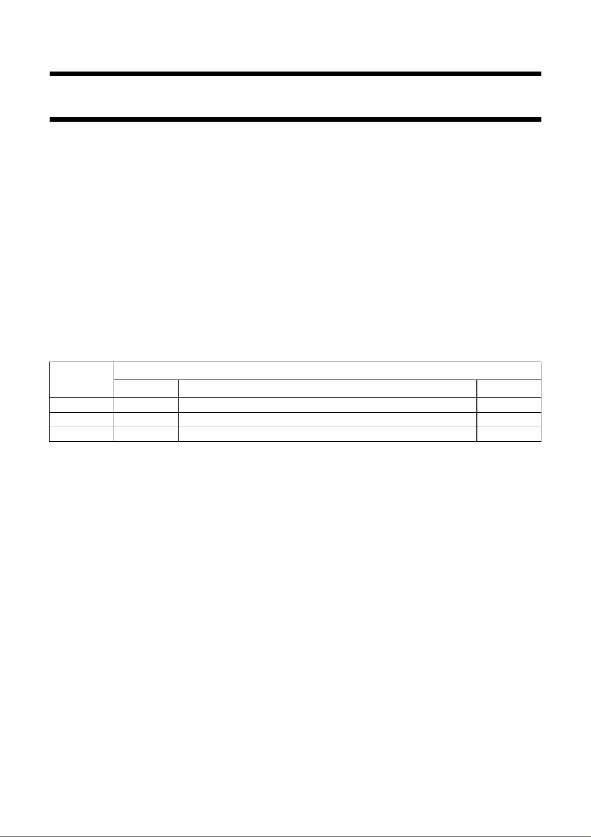
BLOCK DIAGRAM
handbook, full pagewidth
100 pF
DREF
GND
V
CC
2 (1)
4 (2)
IN
1, 7 to 9, 15 to 19,
22 to 25, 31, 32
250
Ω
GNDA GNDD
GAIN
CONTROL
low noise
amplifier
AGC PILOT
10 (4) 27 (12)
TZA3013AHL
TZA3013AU
5 (3)(7, 8) (10)
INQ
PEAK
DETECTOR
single-ended to
differential converter
BIAS
SOURCE
TZA3013A; TZA3013B
V
CC
Ω
2 kΩ
2 kΩ
TESTD
30 (15)
29 (14)
28 (13)
13 (6)
12 (5)
26 (11)
OUTSENSE
OUT
OUTQ
OUTQSENSE
MGT099
V
CC
50Ω50
20 (9)
TESTC
The numbers in brackets refer to the pad numbers of the bare die version.
Fig.1 Block diagram of TZA3013AHL and TZA3013AU.
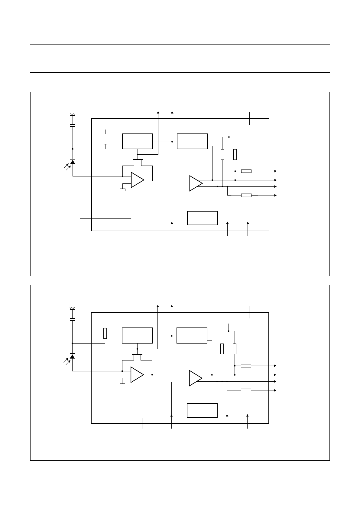
handbook, full pagewidth
100 pF
DREF
V
CC
250
Ω
1
2
IN
GAIN
CONTROL
low noise
amplifier
AGC PILOT
412
PEAK
DETECTOR
TZA3013BU
single-ended to
differential converter
BIAS
SOURCE
37, 8 10
V
CC
50Ω50
9
Ω
V
2 kΩ
2 kΩ
CC
11
15
5
6
13
14
OUTSENSE
OUT
OUTQ
OUTQSENSE
MGU137
GNDA GNDD
INQ
Fig.2 Block diagram of TZA3013BU (bare die only).
2000 Jun 19 3
TESTC
TESTD

Philips Semiconductors Objective specification
SDH/SONET STM16/OC48
TZA3013A; TZA3013B
transimpedance amplifier
PINNING
SYMBOL
GND 1 −−ground ground
DREF 2 1 1 analog
n.c. 3 −−n.c. not connected
IN 4 2 2 input current input; anode of PIN diode should
INQ 5 3 3 input decision level adjust input; note 1
n.c. 6 −−n.c. not connected
GND 7 −−ground ground
GND 8 −−ground ground
GND 9 −−ground ground
AGC 10 4 4 analog
n.c. 11 −−n.c. not connected
OUTQSENSE 12 5 14 analog
OUTQ 13 6 13 output data output; compliment of OUT
n.c. 14 −−n.c. not connected
GND 15 −−ground ground
GND 16 −−ground ground
GND 17 −−ground ground
GND 18 −−ground ground
GND 19 −−ground ground
TESTC 20 9 9 input test input; not used in the application
n.c. 21 −−n.c. not connected
GND 22 −−ground ground
GND 23 −−ground ground
GND 24 −−ground ground
GND 25 −−ground ground
TESTD 26 11 11 input test input; not used in the application
PILOT 27 12 12 analog
OUT 28 13 6 output data output; compliment of OUTQ; note 2
PIN
TZA3013AHL
PAD
TZA3013AU
PAD
TZA3013BU
TYPE DESCRIPTION
bias voltage output for PIN diode; connect
output
output
output
output
cathode of PIN diode to this pin
be connected to this pin; note 1
AGC voltage
data sense output for OUTQ; for test
purposes
pilot tone detection current output
2000 Jun 19 4
Philips Semiconductors Objective specification
SDH/SONET STM16/OC48
TZA3013A; TZA3013B
transimpedance amplifier
SYMBOL
PIN
TZA3013AHL
OUTSENSE 29 14 5 analog
V
CC
30 15 15 supply supply voltage
GND 31 −−ground ground
GND 32 −−ground ground
GNDA − 7 7 ground analog ground
GNDA − 8 8 ground analog ground
GNDD − 10 10 ground digital ground
Notes
1. DC bias voltage = 0.86 V.
2. This pin goes HIGH when current flows into pin IN.
PAD
TZA3013AU
PAD
TZA3013BU
TYPE DESCRIPTION
data sense output for OUT; for test
output
purposes
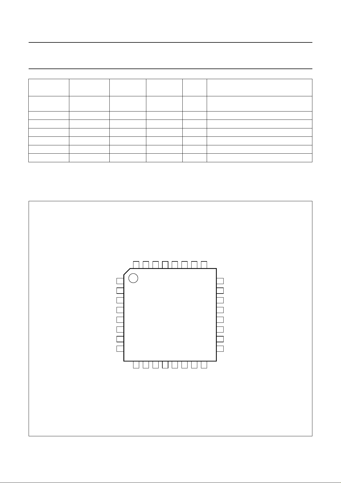
handbook, full pagewidth
GND
DREF
n.c.
INQ
n.c.
GND
GND
CC
GND
GND
32
1
2
3
4
IN
5
6
7
8
9
GND
V
31
30
TZA3013AHL
11
10
n.c.
AGC
OUT
OUTSENSE
29
28
12
13
OUTQ
OUTQSENSE
PILOT
27
14
n.c.
TESTD
26
15
GND
GND
25
16
GND
24
23
22
21
20
19
18
17
MGT100
GND
GND
GND
n.c.
TESTC
GND
GND
GND
Fig.3 Pin configuration of TZA3013AHL.
2000 Jun 19 5
Philips Semiconductors Objective specification
SDH/SONET STM16/OC48
transimpedance amplifier
FUNCTIONAL DESCRIPTION
The TZA3013 is a transimpedance amplifier intended for
use in fibreopticlinks for signal recovery in STM16/OC48
applications. It amplifies the current generated by a photo
detector (PIN diode or avalanche photodiode) and
converts it to a differential output voltage.
The most important characteristics of the TZA3013 are
high receiver sensitivity and wide dynamic range. High
receiver sensitivity is achieved by minimizing
transimpedance amplifier noise.
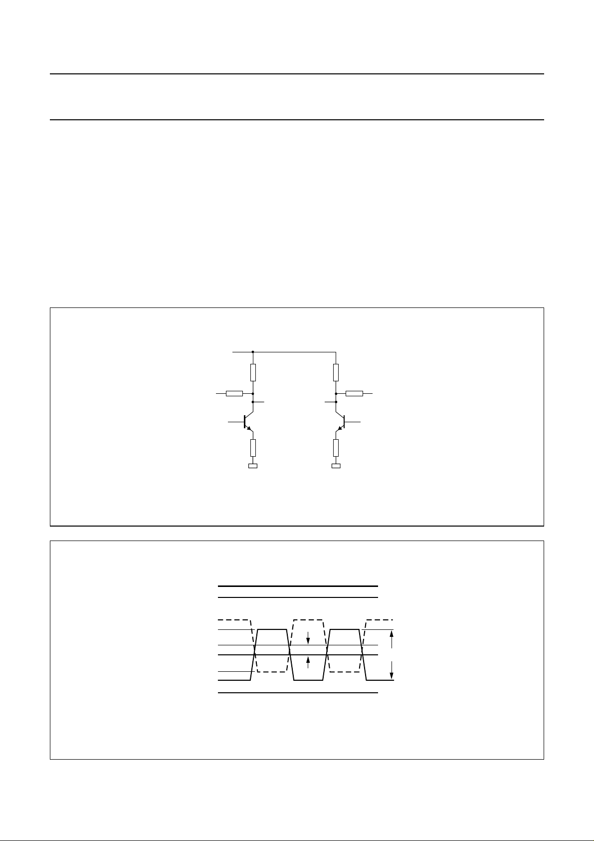
handbook, full pagewidth
OUTSENSE
V
CC
50 Ω
2 kΩ 2 kΩ
OUT
TZA3013A; TZA3013B
The TZA3013 has a wide dynamic range to handle the
signal current generated by the PIN diode which can vary
from 6 µA to 1.7 mA (p-p). This is implemented by an
AGC loop which reduces the preamplifier feedback
resistance so that the amplifier remains linear over the
whole input range. The AGC loop hold capacitor is
integrated on-chip, so an external capacitor is not
required.
A differential amplifier converts the output of the
preamplifiertoadifferentialvoltage.Thedataoutputcircuit
is shown in Fig.4.
The logic level symbol definitions are shown in Fig.5.
50 Ω
OUTQ
OUTQSENSE
handbook, full pagewidth
V
O(max)
V
V
V
O(min)
OQH
V
OH
OQL
V
OL
16 Ω
16 Ω
Fig.4 Data output circuit.
V
OO
MGT102
V
CC
V
o(p-p)
MGR243
Fig.5 Logic level symbol definitions for data outputs OUT and OUTQ.
2000 Jun 19 6
 Loading...