

Philips TZA3005H Datasheet

INTEGRATED CIRCUITS
DATA SH EET
TZA3005H
SDH/SONET STM1/OC3 and
STM4/OC12 transceiver
Product specification
Supersedes data of 1997 Aug 05
File under Integrated Circuits, IC19
2000 Feb 17

Philips Semiconductors Product specification
SDH/SONET STM1/OC3 and STM4/OC12
transceiver
FEATURES
• Supports STM1/OC3(155.52 Mbits/s) and STM4/OC12
(622.08 Mbits/s)
• Supports reference clock frequencies of 19.44, 38.88,
51.84 and 77.76 MHz
• Meets Bellcore, ANSI and ITU-T specifications
• Meets ITU jitter specification typically to a factor of 2.5
• Integral high-frequency PLL for clock generation
• Interface to TTL logic
• Low jitter PECL (Positive Emitter Coupled Logic)
interface
• 4 or 8-bit STM1/OC3 TTL data path
• 4 or 8-bit STM4/OC12 TTL data path
• No external filter components required
• QFP64 package
• Diagnostic and line loopback modes
• Lock detect
• LOS (Loss of Signal) input
• Low power (0.9 W typical)
• Selectable frame detection and byte realignment
• Loop timing
• Forward and reverse clocking
• Squelched clock operation
• Self-biased PECL inputs to support AC coupling.
TZA3005H
GENERAL DESCRIPTION
The TZA3005H SDH/SONET transceiver chip is a fully
integrated serialization/deserialization STM1/OC3
(155.52 Mbits/s) and STM4/OC12 (622.08 Mbits/s)
interfacedevice. It performsallnecessaryserial-to-parallel
and parallel-to-serial functions in accordance with
SDH/SONET transmission standards. It is suitable for
SONET-based applications and can be used in
conjunction with the data and clock recovery unit
(TZA3004), optical front-end (TZA3023 with TZA3034/44)
anda laser driver(TZA3001). A typicalnetworkapplication
is shown in Fig.10.
A high-frequency phase-locked loop is used for on-chip
clock synthesis, which allows a slower external transmit
reference clock to be used. A reference clock of 19.44,
38.88,51.84 or 77.76 MHzcan be usedtosupportexisting
system clocking schemes. The TZA3005H also performs
SDH/SONET frame detection.
The low jitter PECL interface ensures that Bellcore, ANSI,
and ITU-T bit-error rate requirements are satisfied.
The TZA3005H is supplied in a compact QFP64 package.
APPLICATIONS
• SDH/SONET modules
• SDH/SONET-based transmission systems
• SDH/SONET test equipment
• ATM (Asynchronous Transfer Mode) over SDH/SONET
• Add drop multiplexers
• Broadband cross-connects
• Section repeaters
• Fibre optic test equipment
• Fibre optic terminators.
ORDERING INFORMATION
TYPE
NUMBER
TZA3005H QFP64 plastic quad flat package; 64 leads (lead length 1.6 mm);
2000 Feb 17 2
NAME DESCRIPTION VERSION
body 14 × 14 × 2.7 mm
PACKAGE
SOT393-1
Philips Semiconductors Product specification
SDH/SONET STM1/OC3 and STM4/OC12
transceiver
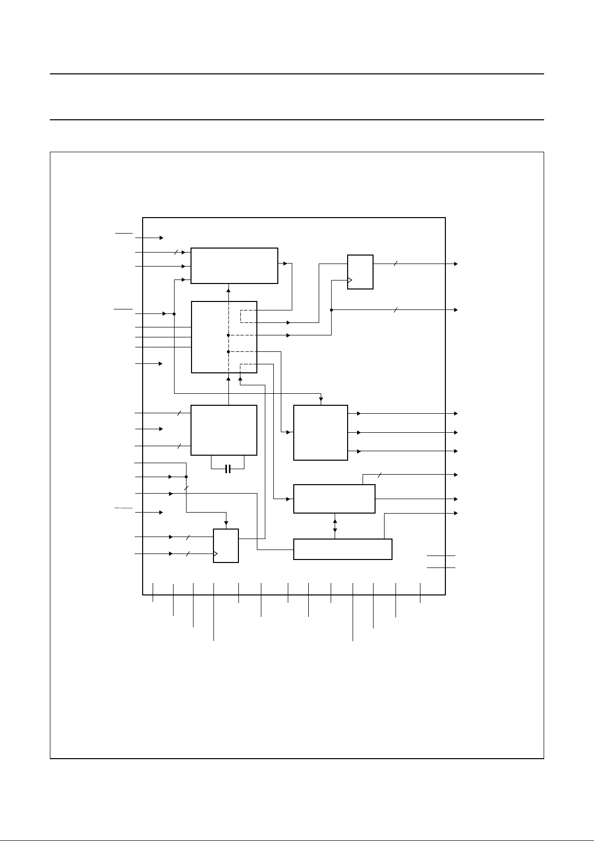
BLOCK DIAGRAM
handbook, full pagewidth
LLEN
TXPD0 to
TXPD7
TXPCLK
MRST
TEST1
TEST2
TEST3
BUSWIDTH
31
53 to 60
61
48
10
11
13
30
8
8:1 OR 4:1
P ARALLEL T O SERIAL
RF
SWITCH
BOX
TRANSMITTER
(1)
D
2
2
TZA3005H
17, 18
21, 20
TZA3005H
TXSD and
TXSDQ
TXSCLK and
TXSCLKQ
REFSEL0 and
REFSEL1
MODE
REFCLK and
REFCLKQ
SDTTL
SDPECL
OOF
DLEN
RXSD and
RXSDQ
RXSCLK and
RXSCLKQ
V
CC(SYNOUT)
3, 4
49
15, 14
22
23
33
32
24, 25
27, 28
GND
2
CLOCK
SYNTHESIZER
2
on-chip capacitor
2
2
2
D
RECEIVER
1
2 5 8, 9 6 7 16 19
V
CCD(SYN)
SYN
V
CCA(SYN)
SYNOUT
DGND
SYN
AGND
12
GND
V
CLOCK
DIVIDER
BY 4 OR BY 8
1:8 OR 1:4
SERIAL TO P ARALLEL
FRAME HEADER DETECT
26
GND
TXOUT
CC(TXOUT)
GND
V
CC(RXCORE)
8
29
V
CC(RXOUT)
RXCORE
36, 37, 39, 40,
41, 43 to 45
34, 42
38, 46
GND
RXOUT
62
63
64
47
35
52
51
SYNCLKDIV
LOCKDET
19MHZO
RXPD0 to
RXPD7
RXPCLK
FP
V
CC(TXCORE)
GND
MGS975
TXCORE
(1) Dashed lines represent normal operation mode.
Fig.1 Block diagram.
2000 Feb 17 3

Philips Semiconductors Product specification
SDH/SONET STM1/OC3 and STM4/OC12
transceiver
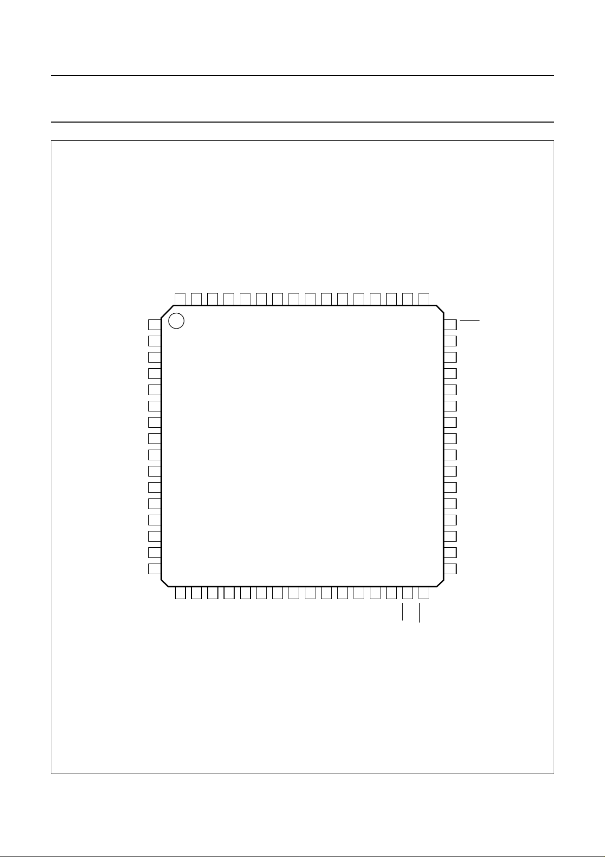
PINNING
SYMBOL PIN TYPE
V
CC(SYNOUT)
GND
SYNOUT
1 S supply voltage (synthesizer output)
2 G ground (synthesizer output)
REFSEL0 3 I reference clock select input 0
REFSEL1 4 I reference clock select input 1
DGND
V
CCD(SYN)
V
CCA(SYN)
AGND
AGND
SYN
SYN
SYN
5 G digital ground (synthesizer)
6 S digital supply voltage (synthesizer)
7 S analog supply voltage (synthesizer)
8 G analog ground (synthesizer)
9 G analog ground (synthesizer)
TEST1 10 I test and control input
TEST2 11 I test and control input
GND 12 G ground
TEST3 13 I test and control input
REFCLKQ 14 I inverted reference clock input
REFCLK 15 I reference clock input
V
CC(TXOUT)
16 S supply voltage (transmitter output)
TXSD 17 O serial data output
TXSDQ 18 O inverted serial data output
GND
TXOUT
19 G ground (transmitter output)
TXSCLKQ 20 O inverted serial clock output
TXSCLK 21 O serial clock output
SDTTL 22 I TTL signal detect input
SDPECL 23 I PECL signal detect input
RXSD 24 I serial data input
RXSDQ 25 I inverted serial data input
V
CC(RXCORE)
26 S supply voltage (receiver core)
RXSCLK 27 I serial clock input
RXSCLKQ 28 I inverted serial clock input
GND
RXCORE
29 G ground (receiver core)
BUSWIDTH 30 I 4/8 bus width select input
LLEN 31 I line loopback enable input (active LOW)
DLEN 32 I diagnostic loopback enable input (active LOW)
OOF 33 I out-of-frame enable input
GND
RXOUT
34 G ground (receiver output)
FP 35 O frame pulse output
RXPD0 36 O parallel data output 0
RXPD1 37 O parallel data output 1
V
CC(RXOUT)
38 S supply voltage (receiver output)
RXPD2 39 O parallel data output 2
RXPD3 40 O parallel data output 3
(1)
DESCRIPTION
TZA3005H
2000 Feb 17 4

Philips Semiconductors Product specification
SDH/SONET STM1/OC3 and STM4/OC12
transceiver
SYMBOL PIN TYPE
RXPD4 41 O parallel data output 4
GND
RXOUT
RXPD5 43 O parallel data output 5
RXPD6 44 O parallel data output 6
RXPD7 45 O parallel data output 7
V
CC(RXOUT)
RXPCLK 47 O receive parallel clock output
MRST 48 I master reset (active LOW)
MODE 49 I serial data rate select STM1/STM4
ALTPIN 50 I test and control input
GND
TXCORE
V
CC(TXCORE)
TXPD0 53 I parallel data input 0
TXPD1 54 I parallel data input 1
TXPD2 55 I parallel data input 2
TXPD3 56 I parallel data input 3
TXPD4 57 I parallel data input 4
TXPD5 58 I parallel data input 5
TXPD6 59 I parallel data input 6
TXPD7 60 I parallel data input 7
TXPCLK 61 I transmit parallel clock input
SYNCLKDIV 62 O transmit byte/nibble clock output (synchronous)
LOCKDET 63 O lock detect output
19MHZO 64 O 19 MHz reference clock output
42 G ground (receiver output)
46 S supply voltage (receiver output)
51 G ground (transmitter core)
52 S supply voltage (transmitter core)
(1)
DESCRIPTION
TZA3005H
Note
1. Pin type abbreviations: O = Output, I = Input, S = Supply, G = Ground.
2000 Feb 17 5
Philips Semiconductors Product specification
SDH/SONET STM1/OC3 and STM4/OC12
transceiver
handbook, full pagewidth
19MHZO
LOCKDET
SYNCLKDIV
TXPCLK
TXPD7
TXPD6
TXPD5
TXPD4
64
63
62
61
60
59
58
57
SYN
SYN
SYN
GND
1
2
3
4
5
6
7
8
9
10
11
12
13
14
15
16
TZA3005H
V
CC(SYNOUT)
GND
SYNOUT
REFSEL0
REFSEL1
DGND
V
CCD(SYN)
V
CCA(SYN)
AGND
AGND
TEST1
TEST2
TEST3
REFCLKQ
REFCLK
V
CC(TXOUT)
TXPD3
56
TXPD2
55
TXPD1
54
CC(TXCORE)
TXPD0
V
53
52
TXCORE
GND
ALTPIN
51
50
MODE
TZA3005H
48
MRST
RXPCLK
47
V
46
CC(RXOUT)
RXPD7
45
RXPD6
44
RXPD5
43
GND
42
RXOUT
RXPD4
41
RXPD3
40
RXPD2
39
V
38
CC(RXOUT)
RXPD1
37
RXPD0
36
FP
35
GND
34
RXOUT
33
OOF
17
TXSD
18
19
TXSDQ
GND
20
TXOUT
TXSCLKQ
22
SDTTL
TXSCLK
23
24
RXSD
SDPECL
21
Fig.2 Pin configuration.
2000 Feb 17 6
25
26
RXSDQ
CC(RXCORE)
V
27
28
RXSCLK
RXSCLKQ
29
30
RXCORE
BUSWIDTH
GND
31
LLEN
32
MGK483
DLEN 49
Philips Semiconductors Product specification
SDH/SONET STM1/OC3 and STM4/OC12
transceiver
FUNCTIONAL DESCRIPTION
Introduction
The TZA3005H transceiver implements SDH/SONET
serialization/deserialization, transmission and frame
detection/recovery functions. The TZA3005Hcan beused
as the front-end for SONET equipment. It handles the
serial receive and transmit interface functions including
parallel-to-serial and serial-to-parallel conversion and
clock generation. A block diagram showing the basic
operation of the chip is shown in Fig.1.
The TZA3005H has a transmitter section, a receiver
section, and an RF switch box. The sequence of
operations is as follows:
• Transmitter operations:
– 4 or 8-bit parallel input
– parallel-to-serial conversion
– serial output.
• Receiver operations:
– serial input
– frame detection
– serial-to-parallel conversion
– 4 or 8-bit parallel output.
The RF switch box receives serial clock and data signals
from the transmitter section, the receiver inputbuffers and
from the clock synthesizer. These signals are routed by
multiplexers to the transmitter section, the transmitter
output, the receiver andto the clock divider, dependingon
the status of the control inputs. The switch box also
supports a number of test and loop modes.
TZA3005H
CLOCK SYNTHESIZER
The clock synthesizer generates a serial output clock
(TXSCLK) which is phase synchronised with the input
reference clock (REFCLK). The serial output clock is
synthesized from one of four SDH/SONET input reference
clock frequencies and can have a frequency of either
155.52 MHz for STM1/OC3 or 622.08 MHz for
STM4/OC12 selected by the MODE input (see Table 1).
Table 1 Transmitter output clock (TXSCLK)
frequency options
MODE
INPUT
0 155.52 MHz STM1/OC3
1 622.08 MHz STM4/OC12
The frequency of the input reference clock is divided to
obtain a frequency of about 19 MHz which is fed to the
phase detector in the PLL. The appropriate divisor is
selected by control inputs REFSEL0 and REFSEL1 as
shown in Table 2.
Table 2 Reference frequency (REFCLK) options
REFSEL1 REFSEL0
0 0 19.44 MHz
0 1 38.88 MHz
1 0 51.84 MHz
1 1 77.76 MHz
TXSCLK
FREQUENCY
OPERATING
MODE
REFCLK
FREQUENCY
Transmitter operation
The transmitter section of the TZA3005H converts
STM1/OC3 or STM4/OC12 byte-serial input data to a
bit-serial output data format. Input data rates of 19.44,
38.88, 77.76 or 155.52 Mbytes/s are converted to an
output data rate of either 155.52 or 622.08 Mbits/s. It also
provides diagnostic loopback (transmitterto receiver), line
loopback (receiver to transmitter) and also loop timing
(transmitter clocked by the receiver clock).
An integral frequency synthesizer, comprising a
phase-locked loop and a divider, can be used to generate
a high-frequency bit clock from an input reference clock
frequency of 19.44, 38.88, 51.84 or 77.76 MHz.
2000 Feb 17 7
To ensure the TXSCLK frequency is accurate enough to
operate ina SONET system,REFCLK must begenerated
from a differential PECL crystal oscillator having a
frequency accuracy better than 4.6 ppm for compliance
with
“ITU G.813 (option 1)”
(option 2)”
To comply with SONET jitter requirements, the maximum
value specified for reference clock signal jitter must be
guaranteed over the 12 kHz to 1 MHz bandwidth (see
Table 3).
.
, or 20 ppm for
“ITU G.813
Philips Semiconductors Product specification
SDH/SONET STM1/OC3 and STM4/OC12
transceiver
Table 3 ITU reference clock signal (REFCLK) jitter limits
MAXIMUM JITTER OF REFCLK
12 kHz TO 1 MHz
56 ps (RMS) STM1/OC3
14 ps (RMS) STM4/OC12
The on-chip PLL contains a phase detector, a loop filter
and a VCO. The phase detector compares the phases of
the VCO and the divided REFCLK signals. The loop filter
convertsthephase detector outputtoa smooth DCvoltage
which controls the VCO frequency and ensures that it is
always 622.08 MHz. In STM1/OC3 mode, the correct
output frequency at TXSCLK is obtained by dividing the
VCO frequency by 4. The loop filter parameters are
optimized for minimal output jitter.
CLOCK DIVIDER
The clock divider generates either a byte rate or a nibble
rate version of the serial output clock (TXSCLK) which is
output on pin SYNCLKDIV (see Table 4).
Table 4 SYNCLKDIV frequency
MODE
INPUT
SYNCLKDIV is intended for use as a byte speed clock for
upstream multiplexing and overhead processing circuits.
Using SYNCLKDIV for upstream circuits ensures a stable
frequency and phase relationship is maintained between
the data in to and out of the TZA3005H.
For parallel-to-serial data conversion, the parallel input
data is transferred from the TXPCLK byte clock timing
domain to theinternally generatedbit clocktiming domain.
The internally generated bit clock does not have to be
phase aligned to the TXPCLK signal but must be
synchronized by the master reset (MRST) signal.
Receiver operation
The receiver section of the TZA3005H converts
STM1/OC3 or STM4/OC12 bit-serial input data to a
parallel data output format. In byte mode, input data rates
of 155.52 or 622.08 Mbits/s are converted to an output
data rate of either 19.44 or 77.76 Mbytes/s. In nibble
BUSWIDTH
0 0 (nibble) 38.88 MHz STM1/OC3
0 1 (byte) 19.44 MHz STM1/OC3
1 0 (nibble) 155.52 MHz STM4/OC12
1 1 (byte) 77.76 MHz STM4/OC12
SYNCLKDIV
FREQUENCY
OPERATING
MODE
OPERATING
MODE
TZA3005H
mode, a 4-bit parallel data stream is generated having a
clock frequency of either 38.88 or 155.52 MHz. It also
provides diagnostic loopback (transmitterto receiver), line
loopback (receiver to transmitter) and squelched clock
operation (transmitter clock to receiver).
FRAME AND BYTE BOUNDARY DETECTION
The frame and byte boundary detection circuit searches
the incoming data for the correct 48-bit frame pattern
whichis asequenceof threeconsecutive A1 bytes ofF0 H
followed immediately by three consecutive A2 bytes of
28 H. Frame pattern detection is enabled and disabled by
the out-of-frame enable input (OOF). Detection isenabled
by a rising edge on pin OOF, and remains enabled while
the level on pin OOF is HIGH. It is disabled when at least
one frame pattern is detected and the level on pin OOF is
no longer HIGH.When framepattern detectionis enabled,
the frame pattern is used to locate byte and frame
boundaries in the incoming data stream (Received Serial
Data (RXSD) or looped transmitter data). The serial to
parallel converterblock uses thelocated byte boundaryto
divide the incoming data stream into bytes for output on
theparallel output databus(RXPD0 to RXPD7). When the
correct 48-bit frame pattern is detected, the occurrence of
the frame boundary is indicated by the Frame Pulse (FP)
signal. When frame pattern detection is disabled, the byte
boundaryis fixed,and only frame patterns whichalign with
the fixed byte boundary produce an output on pin FP.
It is extremely unlikely that random data in an STM1/OC3
or STM4/OC12 data stream will replicate the 48-bit frame
pattern. Therefore, the time taken to detect the beginning
of the frame should be less than 250 µs (as specified in
“ITU G.783”
Once down-stream overhead circuits verify that frame and
byte synchronization are correct, OOF can be set LOW to
prevent the frame search process synchronizing to a
mimic frame pattern.
SERIAL-TO-PARALLEL CONVERTER
The serial-to-parallel converter causes a delay between
thefirst bitof an incomingserial data byteto thestartof the
parallel output of thatbyte. Thedelay dependson the time
taken for the internal parallel load timing circuit to
synchronizethe databyte boundaries tothe fallingedge of
RXPCLK. The timing of RXPCLK is independent of the
byte boundaries. RXPCLK is neither truncated nor
extended during reframe sequences.
) even at extremely high bit error rates.
2000 Feb 17 8

Philips Semiconductors Product specification
SDH/SONET STM1/OC3 and STM4/OC12
transceiver
Transceiver pin descriptions
TRANSMITTER INPUT SIGNALS
Parallel data inputs (TXPD0 to TXPD7)
These areTTL data word inputs. The input data is aligned
with the TXPCLK parallel input clock. TXPD7 is the most
significant bit (corresponding to bit 1 of each PCM word,
the first bit transmitted). TXPD0 is the least significant bit
(corresponding to bit 8 of each PCM word, the last bit
transmitted). Bits TXPD0 to TXPD7 are sampled on the
rising edge of TXPCLK. If a 4-bit bus width is selected,
TXPD7 is the most significant bit and TXPD4 is the least
significant bit. Inputs TXPD0 to TXPD3 are unused.
Parallel clock input (TXPCLK)
This is a TTL input clock signal having a frequency of
either19.44,38.88, 77.76 or 155.52 MHz andadutyfactor
of nominally 50%, to which input data bits TXPD0 to
TXPD7 are aligned. TXPCLK transfers the input data to a
holding register in the parallel-to-serial converter.
The rising edge of TXPCLK samples bits TXPD0 to
TXPD7. After a master reset, one rising edge of TXPCLK
is required to fully initialize the internal data path.
TZA3005H
Signal detect PECL (SDPECL)
This is a single-ended PECL input with an internal
pull-down resistor. This input is driven by an external
optical receiver module to indicate a loss of received
optical power (LOS). SDPECL is active HIGH when
SDTTL is at logic 0 and active LOW when SDTTL is at
logic 1or unconnected. When there is a loss of signal,
SDPECL is inactive and the bit-serial data on pins RXSD
and RXSDQ is internally forced to a constant zero. When
SDPECL is active, the bit-serial data on pins RXSD and
RXSDQ is processed normally (see Table 5).
Signal detect TTL (SDTTL)
This is a single-ended TTL input with an internal pull-up
resistor. This input isdriven byan external optical receiver
module toindicate a loss of received optical power (LOS).
SDTTL is active HIGH when pin SDPECL is logic 0 or
unconnected, and active LOW when pin SDPECL is at
logic 1. When there is a loss of signal, SDTTL is inactive
and the bit-serial data on pins RXSD and RXSDQ is
internallyforced to aconstantzero. When SDTTLisactive,
thebit-serialdata on pins RXSD and RXSDQ isprocessed
normally (see Table 5).
RECEIVER INPUT SIGNALS
Receive serial data (RXSD and RXSDQ)
These are differential PECL serial data inputs, normally
connectedto an opticalreceiver module orto the TZA3004
dataand clockrecovery unit, and clocked byRXSCLK and
RXSCLKQ. These inputs can be AC coupled without
external biasing.
Receive serial clock (RXSCLK and RXSCLKQ)
These are differential PECL recovered clock signals
synchronized to the input data RXSD and RXSDQ. It is
used by the receiver as the master clock for framing and
deserialization functions. These inputs can be AC coupled
without external biasing.
Out-of-frame (OOF)
This is aTTL signalwhich enablesframe patterndetection
logic in the TZA3005H. The frame pattern detection logic
is enabled by a rising edge on pin OOF, and remains
enabled until a frameboundary isdetected andOOF goes
LOW. OOF is an asynchronous signal with a minimum
pulse width of one RXPCLK period (see Fig.3).
If pin SDTTLinstead of pin SDPECL is to be connected to
the optical receiver module, connect pin SDPECL to a
logic HIGH-level to implement an active-LOW signal
detect, or leave pin SDPECL unconnected to implement
an active-HIGH signal detect.
Table 5 SDPECL/SDTTL truth table
SDPECL SDTTL RXPD OUTPUT DATA
0 or floating 0 0
0 or floating 1 or floating RXSD input data
1 0 RXSD input data
1 1 or floating 0
COMMON INPUT SIGNALS
Bus width selection (BUSWIDTH)
This is a TTL signal which selects 4-bit or 8-bit operation
for the transmit and receive parallel interfaces.
BUSWIDTH LOW selects a 4-bit bus width. BUSWIDTH
HIGH selects an 8-bit bus width.
2000 Feb 17 9
 Loading...