

Philips TZA3004HL Datasheet

INTEGRATED CIRCUITS
DATA SH EET
TZA3004HL
SDH/SONET data and clock
recovery unit STM1/4 OC3/12
Product specification
Supersedes data of 1998 Feb 09
File under Integrated Circuits, IC19
2000 Nov 28
Philips Semiconductors Product specification
SDH/SONET data and clock recovery unit
TZA3004HL
STM1/4 OC3/12
FEATURES
• Data and clock recovery up to 622 Mbits/s
• Multi-rate configurable (155 and 622 Mbits/s)
• Differential data input with 2.5 mV (p-p) typical
sensitivity
• Differential Current-Mode Logic (CML) data and clock
outputs with 50 Ω driving capability
• Adjustable CML output level
• Loop mode for system testing
• Bit error rate related loss of signal detection
• Few external components needed
• Single supply voltage
• Power dissipation 370 mW (typical value)
• LQFP48 plastic package.
ORDERING INFORMATION
TYPE
NUMBER
TZA3004HL LQFP48 plastic low profile quad flat package; 48 leads; body 7 × 7 × 1.4 mm SOT313-2
NAME DESCRIPTION VERSION
APPLICATIONS
• DataandclockrecoveryinSTM1/OC3andSTM4/OC12
transmission systems.
DESCRIPTION
The TZA3004HL is a data and clock recovery IC intended
for use in Synchronous Digital Hierarchy (SDH) and
Synchronous Optical Network (SONET) systems. The
circuit recovers data and extracts the clock signal from an
incoming bitstream up to 622 Mbits/s. It can be configured
for use in STM1/OC3 and STM4/OC12 systems.
PACKAGE
2000 Nov 28 2
Philips Semiconductors Product specification
SDH/SONET data and clock recovery unit
STM1/4 OC3/12
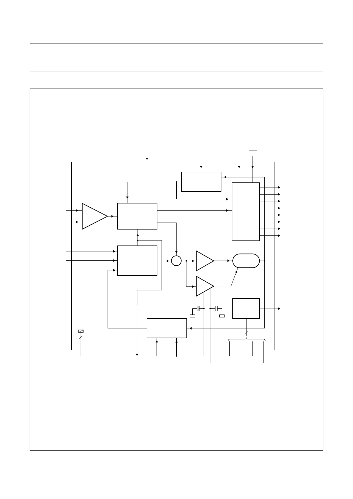
BLOCK DIAGRAM
andbook, full pagewidth
DIN
DINQ
33
34
LOS
39
ALEXANDER
PHASE
DETECTOR
enable
SEL155
30
FREQUENCY
DIVIDER 1
4/16
TZA3004HL
AREF
DATA
AND
CLOCK
OUTPUT
TZA3004HL
ENL
1
48
42
DOUT
43
DOUTQ
45
COUT
46
COUTQ
6
DLOOP
7
DLOOPQ
3
CLOOP
4
CLOOPQ
CREF
CREFQ
21
22
17
2, 5, 8, 10, 11, 14, 17,
20, 23, 26, 29, 32, 35,
38, 41, 44, 47
GND
FREQUENCY
WINDOW
DETECTOR
(1000 ppm)
FREQUENCY
12 24 25
DREF19LOCK
DIVIDER 2
64/128
9
+
∫
dt
CAPDOQDREF39
CAPUPQ
proportional
path
integrating
path
130 pF130 pF
1516
V
EE1
VCRO
POWER
CONTROL
4
27
V
EE3
V
EE2
37
PC
28
31
MGU255
V
EE4
Fig.1 Block diagram.
2000 Nov 28 3
Philips Semiconductors Product specification
SDH/SONET data and clock recovery unit
STM1/4 OC3/12
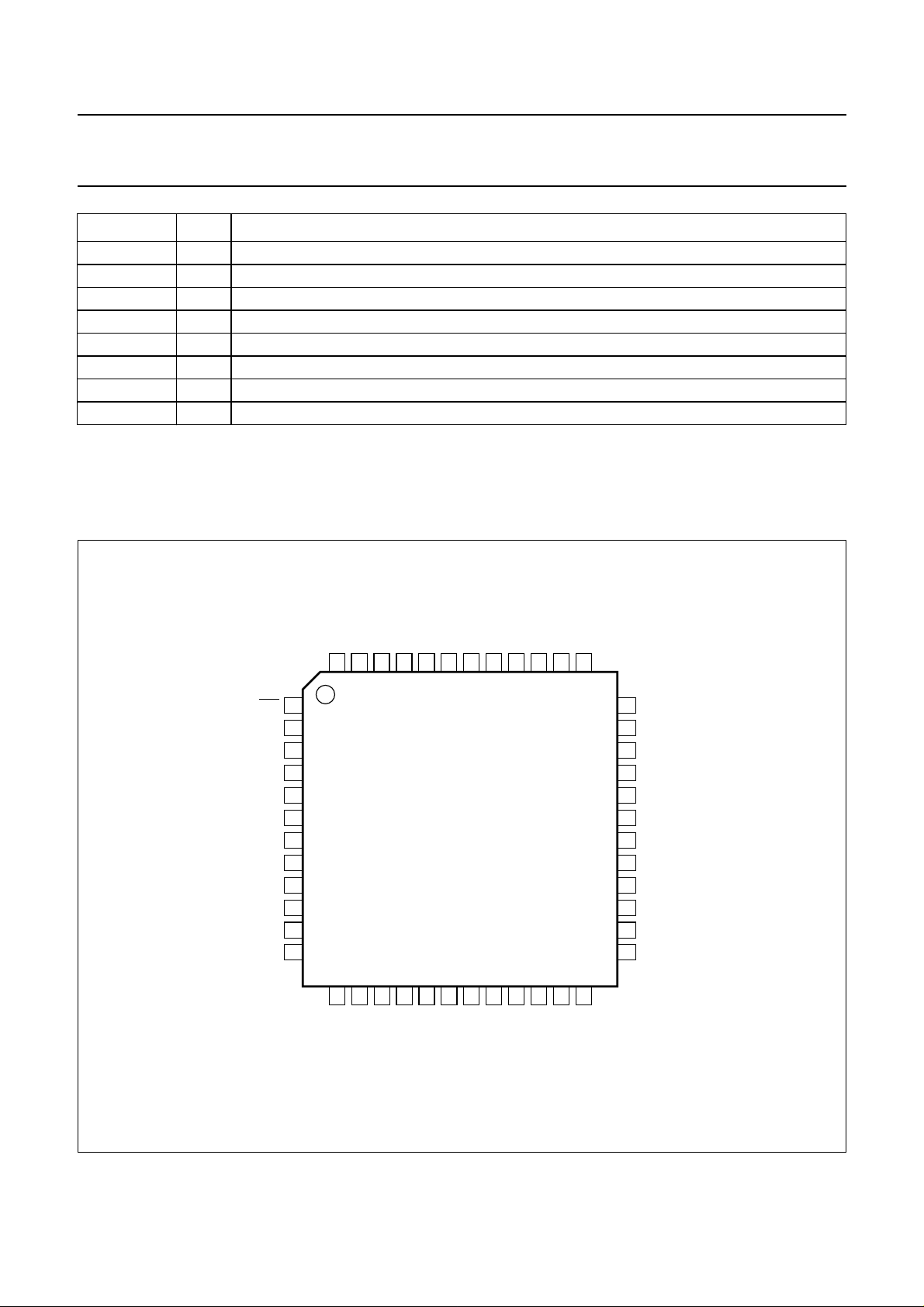
PINNING
SYMBOL PIN DESCRIPTION
ENL 1 loop mode enable input (active LOW)
GND 2 ground; note 1
CLOOP 3 clock output in loop mode (differential)
CLOOPQ 4 inverted clock output in loop mode (differential)
GND 5 ground; note 1
DLOOP 6 data output in loop mode (differential)
DLOOPQ 7 inverted data output in loop mode (differential)
GND 8 ground; note 1
DREF19 9 reference frequency select input 1 (see Table 3)
GND 10 ground; note 1
GND 11 ground; note 1
LOCK 12 phase lock detection output
i.c. 13 internally connected; note 2
GND 14 ground; note 1
CAPUPQ 15 external loop filter capacitor connection
CAPDOQ 16 external loop filter capacitor return connection
GND 17 ground; note 1
i.c. 18 internally connected; note 2
i.c. 19 internally connected; note 2
GND 20 ground; note 1
CREF 21 reference clock input (differential)
CREFQ 22 inverting reference clock input (differential)
GND 23 ground; note 1
DREF39 24 reference frequency select input 2 (see Table 3)
V
EE1
GND 26 ground; note 1
V
EE2
V
EE3
GND 29 ground; note 1
SEL155 30 STM mode select input 3 (see Table 2)
V
EE4
GND 32 ground; note 1
DIN 33 data input (differential)
DINQ 34 inverting data input (differential)
GND 35 ground; note 1
i.c. 36 internally connected; note 2
PC 37 control output for negative power supply
GND 38 ground; note 1
LOS 39 loss of signal detection output
i.c. 40 internally connected; note 2
25 negative supply voltage (−3.3 V); note 3
27 negative supply voltage (−3.3 V); note 3
28 negative supply voltage (−3.3 V); note 3
31 negative supply voltage (−3.3 V); note 3
TZA3004HL
2000 Nov 28 4
Philips Semiconductors Product specification
SDH/SONET data and clock recovery unit
TZA3004HL
STM1/4 OC3/12
SYMBOL PIN DESCRIPTION
GND 41 ground; note 1
DOUT 42 data output in normal mode (differential)
DOUTQ 43 inverted data output in normal mode (differential)
GND 44 ground; note 1
COUT 45 clock output in normal mode (differential)
COUTQ 46 inverted clock output in normal mode (differential)
GND 47 ground; note 1
AREF 48 reference voltage input for controlling voltage swing on data and clock outputs
Notes
1. ALL GND pins must be connected; do not leave one single GND pin unconnected.
2. ALL pins denoted ‘i.c.’ have internal connections; external connections to these pins should not be made.
3. ALL VEE pins must be connected; do not leave one single VEE pin unconnected.
handbook, full pagewidth
ENL
GND
CLOOP
CLOOPQ
GND
DLOOP
DLOOPQ
GND
DREF19
GND
GND
LOCK
COUTQ
GND
47
14
GND
COUT
46
45
15
16
CAPUPQ
CAPDOQ
GND
44
TZA3004HL
17
GND
AREF
48
1
2
3
4
5
6
7
8
9
10
11
12
13
i.c.
DOUT
DOUTQ
43
42
18
19
i.c.
i.c.
GND
41
20
GND
i.c.
40
21
CREF
GND
LOS
39
38
22
23
GND
CREFQ
PC
24 37
DREF39
36
35
34
33
32
31
30
29
28
27
26
25
MGU254
i.c.
GND
DINQ
DIN
GND
V
EE4
SEL155
GND
V
EE3
V
EE2
GND
V
EE1
Fig.2 Pin configuration.
2000 Nov 28 5
Philips Semiconductors Product specification
SDH/SONET data and clock recovery unit
STM1/4 OC3/12
FUNCTIONAL DESCRIPTION
The TZA3004HL recovers data and clock signals from an
incoming high speed bitstream. The input signal on
pins DIN and DINQ is buffered and amplified by the input
circuitry (see Fig.1). The signal is then fed into the
Alexander phase detector where the phase of the
incoming data signal is compared with that of the internal
clock. If the signals are out of phase, the phase detector
generates correction pulses (up or down) that shift the
phase of the Voltage Controlled Ring Oscillator (VCRO)
output in discrete amounts (∆ϕ) until the clock and data
signals are in phase. The technique used is based on
principles first proposed by J. D. H. Alexander, hence the
name of the phase detector.
Data sampling
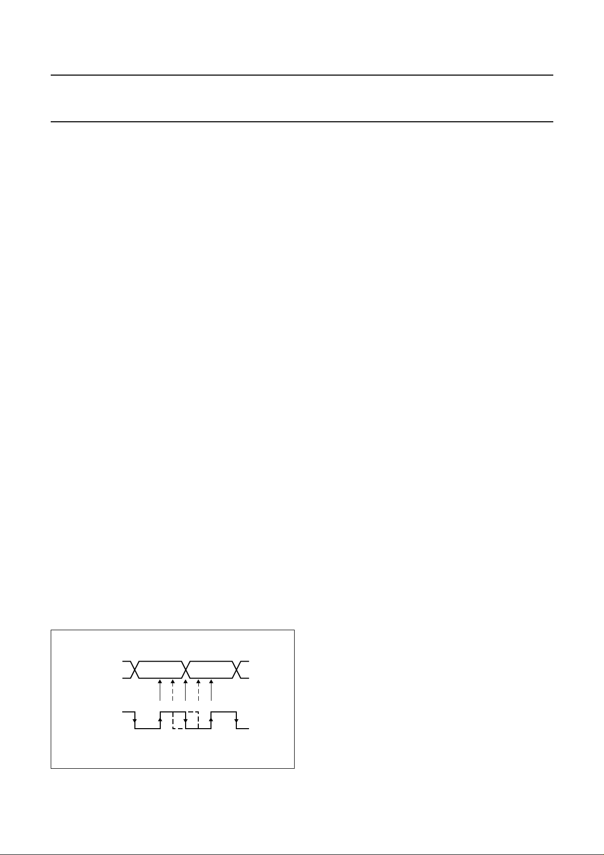
As shown in Fig.3, the eye pattern of the incoming data is
sampled at three instants A, T and B. When clock and
data signals are synchronized (locked):
• A is the centre of the data bit
• T is in the vicinity of the next transition
• B is in the centre of the bit following the transition.
If the same level is recorded at both A and B, a transition
has not occurred and no action is taken. However, if the
levels at A and B are different, a transition has occurred
and the phase detector uses the level at T to determine
whether the clock was too early or too late with respect to
the data transition.
If the levels at A and T are the same but are different from
the level at B, the clock was too early and needs to be
slowed down a little. The Alexander phase detector then
generates a down pulse which stretches a single output
pulse from the ring oscillator by approximately 0.25%
which is 4 ps of the 1.6 ns bit period in the STM4/OC12
mode. This forces the VCRO to run at a slightly lower
frequency for one bit period. The phase of the clock signal
is thus shifted fractionally with respect to the data signal.
TZA3004HL
If the levels at B and T are the same but are different from
the level at A, the clock was too late and needs to be
speeded up for synchronization. The phase detector
generatesanuppulseforcingthe VCRO to run at a slightly
higherfrequency(+0.25%)foronebitperiod.Thephaseof
theclocksignalisshiftedwithrespecttothedatasignal(as
above, but in the opposite direction). While making these
phase adjustments, only the proportional path is active.
This type of loop is known as a Bang/Bang Phase-Locked
Loop (PLL) as the instantaneous frequency of the VCRO
changes in one of two discrete steps (±0.25%).
If the phase and the frequency of the VCRO are incorrect,
a long train of up or down pulses is generated. This train of
pulses is integrated to generate a control voltage that is
used to shift the centre frequency of the VCRO. Once the
correct frequency has been established, only the phase
will need to be adjusted for synchronization. The
proportional path adjusts the phase of the clock signal,
whereas the integrating path adjusts the centre frequency.
Frequency window detector
The frequency window detector checks the VCRO
frequency which has to be within a 1000 ppm (parts per
million) window around the required frequency.
It compares the output of frequency divider 2 with the
reference frequency on pins CREF and CREFQ
(19.44 or 38.88 MHz;see Table 3). IftheVCRO frequency
is found to be outside this window, the frequency window
detectordisablestheAlexander phase detector and forces
the VCRO output to a frequency within the window. The
phase detector then starts acquiring lock again. Due to the
loosecoupling of 1000 ppm,thereferencefrequencydoes
notneed to be highly accurate or stable.Any crystal based
oscillator that generates a reasonably accurate frequency
(e.g. 100 ppm) can be used.
Since sampling point A is always in the centre of the eye
pattern when the data and clock signals are in phase
(locked), the values recorded at this point are taken as the
retrieved data. The data and clock signals are available at
the CML output buffers, that are capable of driving a 50 Ω
load.
handbook, halfpage
DATADATA
ATB
CLOCK
MGK143
Fig.3 Data sampling.
2000 Nov 28 6
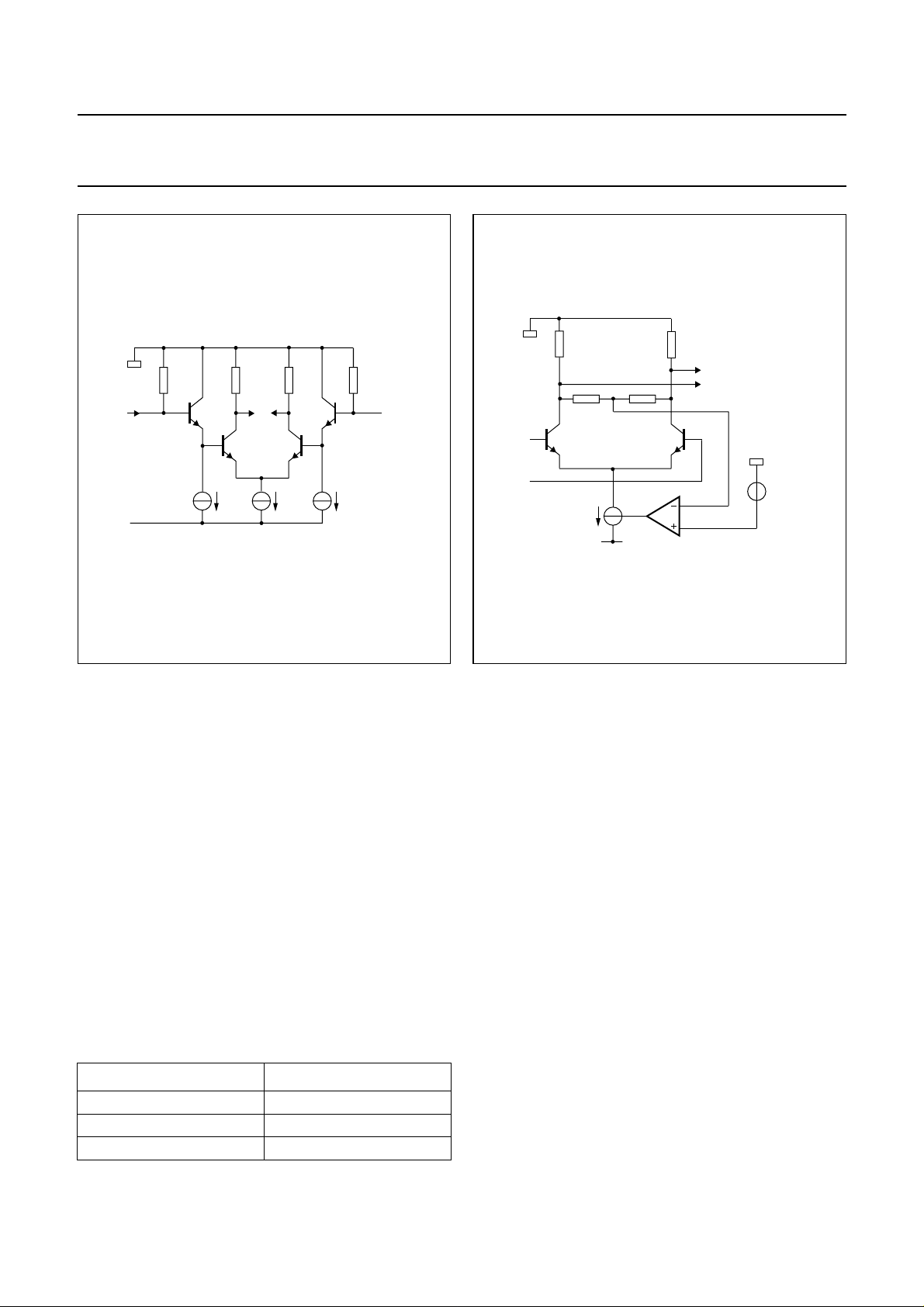
RF data and clock input circuit
The schematic of the input circuit is shown in Fig.4.
RF data and clock output circuit
The schematic of the output circuit is shown in Fig.5.
Philips Semiconductors Product specification
SDH/SONET data and clock recovery unit
STM1/4 OC3/12
handbook, halfpage
50 Ω50 Ω
MGL669
DINQ,
CREFQ
DIN,
CREF
VEE
TZA3004HL
100 Ω100 Ω
DOUTQ, COUTQ
DOUT, COUT
V
AREF
V
EE
MGL670
Fig.4 RF data and clock input circuit.
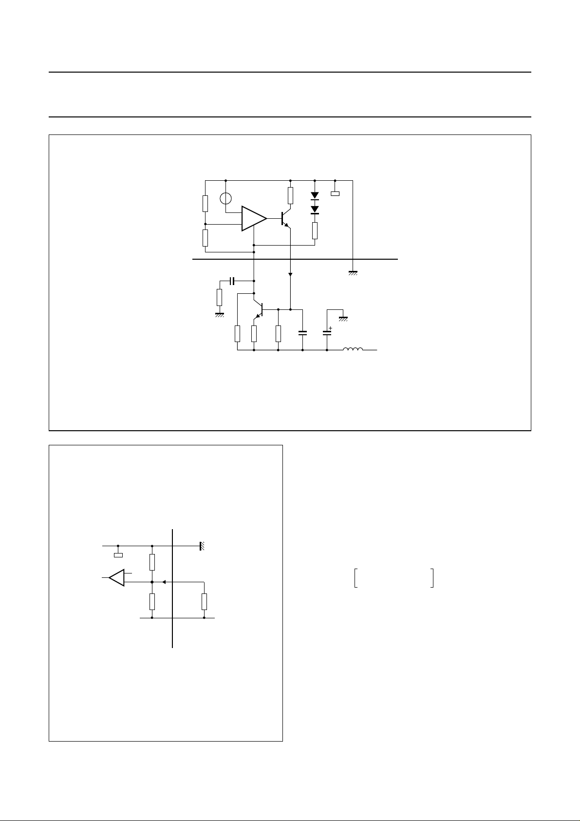
Power supply and power control loop
The TZA3004HL contains an on-board voltage regulator.
An external power transistor is needed to deliver the
supply to this circuit. The external circuit requirement is
straightforward and needs few components. A suitable
circuit with a power supply of −4.5 V is illustrated in Fig.6.
The inductor shown is an RF choke with an impedance
greater than 50 Ω at frequencies higher than 2 MHz. Any
transistor with a β of approximately 100 and enough
current sink capability can be used.
The TZA3004HL can also be used with a power supply of
−5.0 or −5.2 V. The only adaptation to be made to the
power control circuit is to change the emitter resistor R1
(see Fig.6 and Table 1).
As long as the power supply rejection ratio is greater than
60 dB for all frequencies, a different power supply
configuration could be used.
Table 1 Value of resistor R1.
POWER SUPPLY RESISTOR R1
−4.5 V 2.0 Ω
−5.0 V 6.8 Ω
−5.2 V 8.2 Ω
Fig.5 RF data and clock output circuit.
Output amplitude reference
The voltage swing at the CML-compatible output stages
(pins DOUT, DOUTQ, COUT, COUTQ, DLOOP,
DLOOPQ, CLOOP and CLOOPQ) can be controlled by
adjusting the voltage on pin AREF (see Fig.7). An internal
voltage divider of 500 Ω and 16 kΩ connected between
ground and VEE initially fixes this level.
In most applications the outputs will be DC-coupled to
a load of 50 Ω. The output level regulation circuit will
maintain a 200 mV (p-p) single-ended swing across this
load. The voltage on pin AREF is half the single-ended
peak-to-peak value of the output signal (−100 mV).
No adjustments are necessary with DC-coupling.
When the outputs are AC-coupled, the voltage on
pin AREF is half the single-ended peak-to-peak value of
the output signal multiplied by a factor
RLRo+
-------------------R
L
where RL is the external load and Ro is the output
impedance of the TZA3004HL (100 Ω).
2000 Nov 28 7
Philips Semiconductors Product specification
SDH/SONET data and clock recovery unit
STM1/4 OC3/12
handbook, full pagewidth
2 Ω
100 nF
1 kΩ
BAND GAP
REFERENCE
V
EE
β ≈ 100
R1
2 Ω
1
kΩ
PC
3.3
nF
GND
1 µF
TZA3004HL
on chip
off chip
(1)
L1
−4.5 V
MGU253
(1) L1 = RF choke type Murata BLM21, 1 µH.
Fig.6 Schematic diagram of TZA3004HL power control loop.
handbook, halfpage
500 Ω
16 kΩ R
GND
AREF
V
EE
If the outputs are AC-coupled, the formulae for calculating
the required voltage on pin AREF and the value of the
resistor connected between pins AREF and VEE are:
V
AREF
RLRo+
-------------------R
L
×–=
0.5V
swing
(1)
and:
V
EE
V
AREF
AREF
R1
×
---------------- -
V
AREF
=
------------------------------------------------------------1
R
AREF
R1
×–
------- -
R2
where R1 = 500 Ω, R2 = 16 kΩ and VEE= −3.3 V.
V
EE
---------------- V
AREF
1–
(2)
1–
To maintain a single-ended swing of 200 mV (p-p) across
a50ΩAC-coupled load, the voltage onpin AREF must be
off chipon chip
MGL667
100 mV–
50 + 100()Ω
× 300 mV.–=
---------------------------------
50 Ω
Fig.7 Functionality of pin AREF.
2000 Nov 28 8
This can be achieved by connecting a 7.3 kΩ resistor
between pins AREF and VEE.
Philips Semiconductors Product specification
SDH/SONET data and clock recovery unit
STM1/4 OC3/12
External capacitor for loop filter
The loop filter is an integrator with a built-in capacitance of
2 × 130 pF. To ensure loop stability while the frequency
window detector is active, an external capacitance of
200 nF should be connected between pins CAPUPQ
and CAPDOQ.
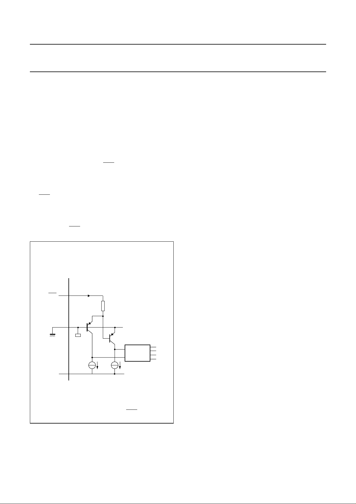
Loop mode enable
The loop mode is provided for system testing (see Fig.8).
Loop mode is enabled by applying a voltage lower than
0.8 V (TTL LOW-level) to pin ENL. In loop mode, the
outputs on pins DLOOP, DLOOPQ, CLOOP and
CLOOPQ are switched on.
A voltage higher than 2.0 V (TTL HIGH-level) applied to
pin ENL switches on pins DOUT, DOUTQ, COUT
and COUTQ while pins DLOOP, DLOOPQ, CLOOP
and CLOOPQ are disabled to minimize power
consumption.
Connecting pin ENL to VEE(−3.3 V) enables all outputs.
handbook, halfpage
off chip on chip
ENL
36 kΩ
GND
DECODER
LOGIC
V
EE
MGL668
TZA3004HL
Lock detection
The LOCK output can be interpreted as an indication that
the reference clock is present on pin CREF and that the
acquisition aid (frequency window detector) is functioning
properly.
LOCK is an open-collector TTL output to be connected via
a10kΩpull-up resistor to a positive supply voltage. If the
VCO frequency is within a 1000 ppm window around the
desired frequency, pin LOCK will stay at HIGH-level. If no
reference clock is present, or the VCO is outside the
1000 ppm window, pin LOCK will be at a LOW-level. The
logic level on pin LOCK does not indicate locking of the
PLL to the incoming data; this is done by the signal on
pin LOS.
Loss of signal detection
The Loss Of Signal (LOS) function is closely related to the
functionalityof the Alexander phase detector (see Fig.3 for
the meaning of A, B and T in this section).
The phase detector takes no action if there has been no
transition and the values at sample points A and B are the
same. However, if levels A and B are equal but level at T
is different, even with no transition, the incorrect level at T
could lead to a bit error. This incorrect level could be due
tonoiseor from poor signal integrity. The cumulative affect
of bit errors could cause the PLL to lose lock and the LOS
alarm to be asserted. The LOS alarm assert level is
approximately Bit Error Rate (BER) = 5 × 10⁻² and the
de-assert level is approximately BER = 1 × 10⁻³.
LOS detection functions correctly if the input signal is
larger than the input offset of the TZA3004HL. If the input
signal is smaller, it is masked by the input offset and
interpreted as consecutive bits of the same sign, thus
obstructingLOS detection. In practice, an optical front-end
device with a noise level larger than the specified offset of
the TZA3004HL will ensure proper LOS indication.
The LOS detection is BER related, but not dependent on
the data stream content or protocol. Therefore, an
SDH/SONET data stream is no prerequisite for a proper
LOS function. Since the LOS function of the TZA3004HL
isderived from digital signals, it is a good supplement to an
analog, amplitude based, LOS indication.
Fig.8 Input circuit of pin ENL.
2000 Nov 28 9
Pin LOS is an open-collector TTL compatible output. that
needs a pull-up resistor connected to a positive supply
voltage to function.
The LOS pin will be at a(TTL) HIGH-level if the data signal
is absent on pins DIN and DINQ or if BER > 5 × 10⁻²;
otherwise pin LOS will be at LOW-level if BER < 1 × 10⁻³.
Philips Semiconductors Product specification
SDH/SONET data and clock recovery unit
STM1/4 OC3/12
STM mode selection
The VCRO has a very wide tuning range. However, the
performance of the TZA3004HL is optimized for
SDH/SONET bit rates.
Due to the nature of the PLL, the very wide tuning range is
a necessity for proper lock behaviour over the guaranteed
temperature range, aging and batch-to-batch spread.
Though it may seem that the TZA3004HL is capable of
recovering bit rates other than SDH/SONET (STM1/OC3
and STM4/OC12), lock behaviour cannot be guaranteed.
The required SDH/SONET bit rate is selected by
connecting pin SEL155 to the ground plane or to the
supply voltage VEE (see Table 2):
• For STM4/OC12 (622.08 Mbits/s) operation, pin
SEL155 is to be connected to ground (pin GND)
• For STM1/OC3 (155,52 Mbits/s) operation, pin SEL155
is to be connected to VEE.
The connection to VEEor ground carries a current of a few
milliamperes and should have low resistance and
inductance; short printed-circuit board tracks are
recommended. In some cases it may be necessary to add
a decoupling capacitor near the selection pin to provide
a clean return path for RF signals.
TZA3004HL
Reference frequency select
A reference clock signal of 19.44 or 38.88 MHz must be
connected to pins CREF and CREFQ. Pins DREF19
and DREF39 are used to select the appropriate output
frequency at frequency divider 2 (see Table 3).
To minimize the adverse influence of reference clock
crosstalk, a differential signal with an amplitude from
75 to 150 mV (p-p) is advised.
Sincethe reference clock is only used as an acquisition aid
for the PLL of the frequency window detector, the quality
of the reference clock (i.e. phase noise) is not important.
There is no phase noise specification imposed on the
reference clock generator and even frequency stability
may be in the order of 100 ppm. In general, most
inexpensive crystal-based oscillators are suitable.
There are two application possibilities for the TZA3004HL
reference clock:
• A fixed reference clock frequency, here it is best to
connect pins DREF19 and DREF39 using a short track
or a via to the ground plane or the supply voltage V
• Aselectable reference clock frequency in which the pins
can be controlled through low-ohmic switching FETs,
e.g. BSH103 or equivalent (low R
DSon
).
EE
Whenthe TZA3004HL is used in anapplicationwith a fixed
datarate it is best to connect pin SEL155 byashortcopper
trace or a via to the ground plane or supply voltage VEE.
If a selectable reference clock frequency is required in the
application, the pin can be controlled through a low-ohmic
switching FET, e.g. BSH103 or equivalent (low R
DSon
).
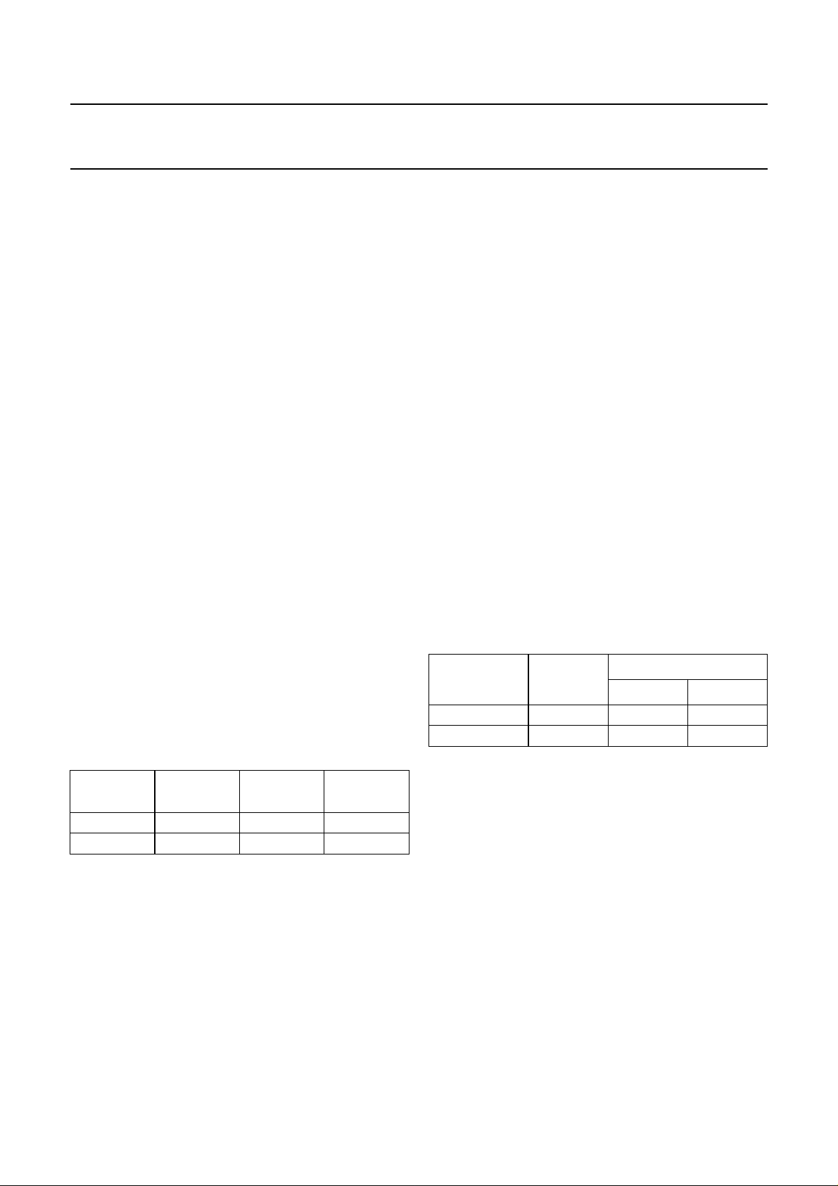
Table 2 STM mode select
MODE
BIT RATE
(Mbits/s)
STM1/OC3 155.52 16 V
DIVISION
FACTOR
LEVEL ON
PIN SEL155
EE
STM4/OC12 622.08 4 ground
Table 3 Reference frequency selection
FREQUENCY
(MHz)
DIVISION
FACTOR
LEVEL ON PIN
DREF19 DREF39
38.88 64 ground V
19.44 128 V
EE
EE
V
EE
2000 Nov 28 10
 Loading...