

Philips TZA3001U, TZA3001BHL Datasheet

INTEGRATED CIRCUITS
DATA SH EET
TZA3001AHL; TZA3001BHL;
TZA3001U
SDH/SONET STM4/OC12
laser drivers
Objective specification
File under Integrated Circuits, IC19
1997 Sep 08
Philips Semiconductors Objective specification
SDH/SONET STM4/OC12
laser drivers
FEATURES
• 622 Mbits/s data input, both Current-Mode Logic (CML)
and Positive Emitter-Coupled Logic (PECL) compatible
(800 mV peak-to-peak maximum)
• Adaptive laser output control, stabilizing optical ONE
and ZERO levels
• Optional external (non-adaptive) control of laser
modulation and biasing currents
• Automatic Laser Shutdown (ALS)
• Few external components required
• Rise and fall times typically 120 ps
• Jitter <50 mUI peak-to-peak
• RF output current sinking capability of 60 mA
• Bias current sinking capability of 90 mA
• Power dissipation typically 475 mW
• Low cost LQFP32 plastic package
• Single 5 V power supply.
TZA3001AHL
• Laser alarm output for signalling extremely low and high
bias current conditions.
TZA3001AHL;
TZA3001BHL; TZA3001U
TZA3001U
• Naked die version with combined bias alarm and loop
mode functionality.
DESCRIPTION
The TZA3001AHL, TZA3001BHL and TZA3001U are fully
integrated laser drivers for STM4/OC12 (622 Mbits/s)
systems, incorporating the RF path between the data
multiplexer and the laser diode. Since the bias and
modulation control circuits are integrated on the IC, the
external component count is low (only decoupling
capacitors and adjustment resistors are required).
The TZA3001AHL features an alarm function for signalling
extreme bias current conditions. The alarm low and high
threshold levels can be adjusted to suit the application
using only a resistor. An additional RF data input is
provided with the TZA3001BHL to facilitate remote (loop
mode) system testing.
The TZA3001U is a naked die version for use in compact
laser module designs. The die contains 40 pads and
features the combined functionality of the TZA3001AHL
and TZA3001BHL.
TZA3001BHL
• Loop mode for testing STM4 622 Mbits/s optical
interfaces; CML and PECL compatible.
ORDERING INFORMATION
TYPE
NUMBER
TZA3001AHL LQFP32
TZA3001BHL LQFP32
TZA3001U − naked die; 2000 × 2000 × 380 µm −
NAME DESCRIPTION VERSION
plastic low profile quad flat package; 32 leads; body 5 × 5 × 1.4 mm
plastic low profile quad flat package; 32 leads; body 5 × 5 × 1.4 mm
APPLICATIONS
• SDH/SONET STM4/OC12 optical transmission systems
• SDH/SONET STM4/OC12 optical laser modules.
PACKAGE
SOT401-1
SOT401-1
1997 Sep 08 2
Philips Semiconductors Objective specification
SDH/SONET STM4/OC12
laser drivers
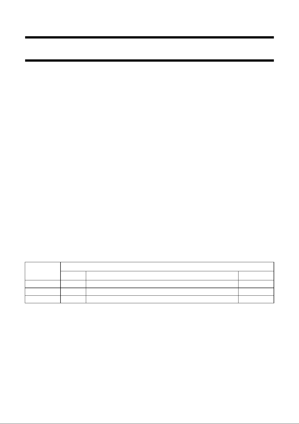
BLOCK DIAGRAMS
handbook, full pagewidth
DIN
DINQ
TZA3001AHL; TZA3001BHL;
ALARMLO
28
29
ALARM
26
data input
(differential)
TONE
4
TZA3001AHL
19, 20
7
27, 30
411
V
CC(R)
V
CC(G)
CC(B)
V
31
10
ALS
ALARMHITZERO
215
LASER
CONTROL
BLOCK
CURRENT
SWITCH
BAND GAP
REFERENCE
1, 3, 8, 9,
11, 14, 16, 17
24, 25, 32
GND
18
MGK271
2
MONIN
22
ONE
23
ZERO
13
LA
12
LAQ
15
BIAS
6
BGAP
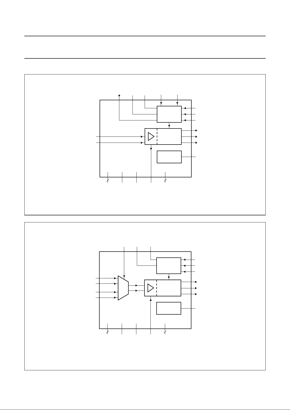
TZA3001U
handbook, full pagewidth
DIN
DINQ
DLOOP
DLOOPQ
Fig.1 Block diagram: TZA3001AHL.
TONE
10
CC(B)
4
TZERO
31
ALS
LASER
CONTROL
BLOCK
CURRENT
SWITCH
BAND GAP
REFERENCE
1, 3, 8, 9,
11, 14, 16, 17
24, 25, 32
GND
22
23
13
12
15
MGK270
2
MONIN
ONE
ZERO
LA
LAQ
BIAS
6
BGAP
ENL
26 5
28
29
19
20
MUX
TZA3001BHL
18, 21
7
27, 30
411
V
V
V
CC(R)
CC(G)
Fig.2 Block diagram: TZA3001BHL.
1997 Sep 08 3
Philips Semiconductors Objective specification
SDH/SONET STM4/OC12
laser drivers
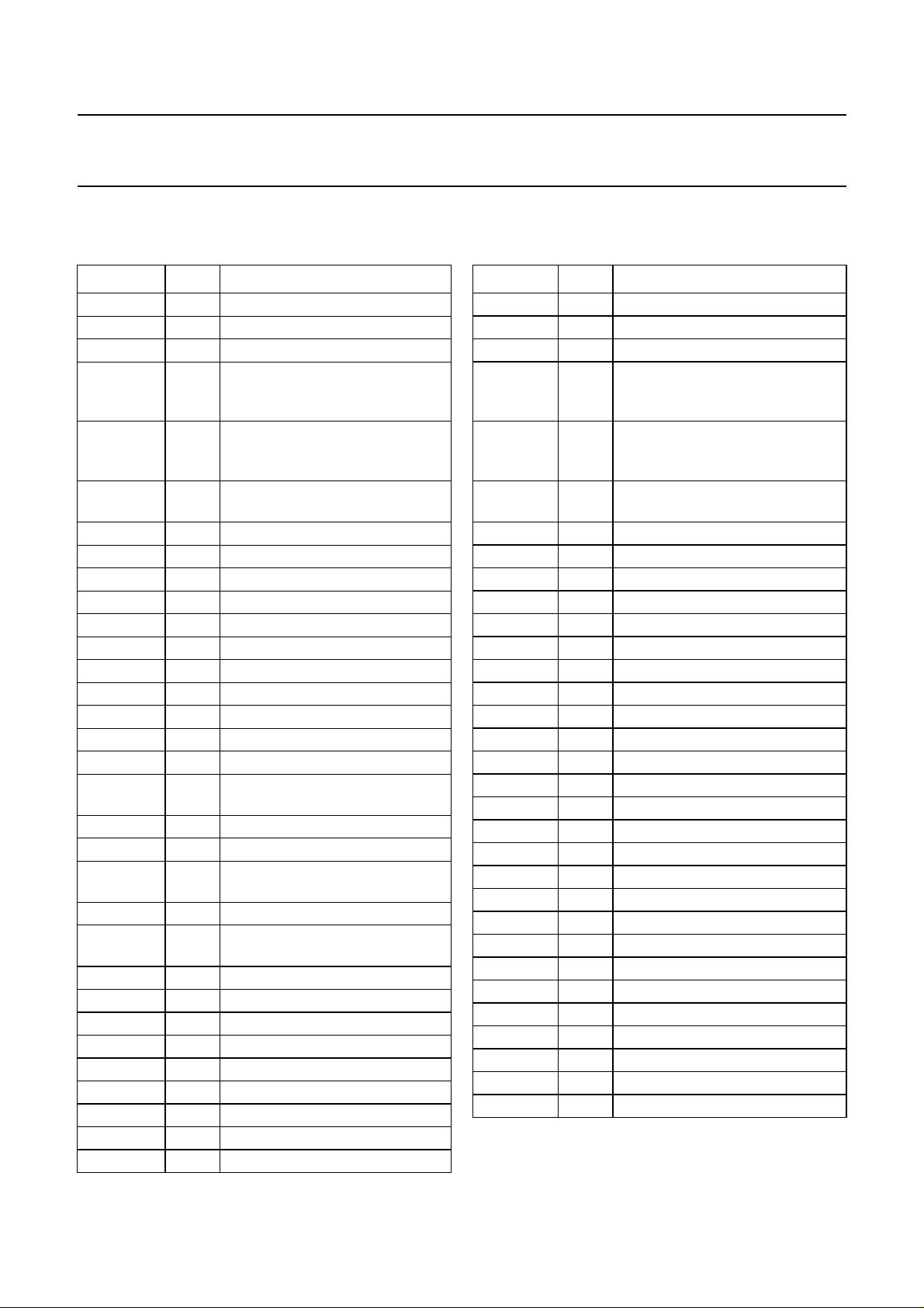
PINNING
TZA3001AHL
SYMBOL PIN DESCRIPTION
GND 1 ground
MONIN 2 monitor photo diode current input
GND 3 ground
TONE 4 connection for external capacitor
used to set optical ONE control
loop time constant (optional)
TZERO 5 connection for external capacitor
used to set optical ZERO control
loop time constant (optional)
BGAP 6 connection for external band gap
decoupling capacitor
V
CC(G)
GND 8 ground
GND 9 ground
V
CC(B)
GND 11 ground
LAQ 12 inverted laser modulation output
LA 13 laser modulation output
GND 14 ground
BIAS 15 laser bias current output
GND 16 ground
GND 17 ground
ALARMHI 18 maximum bias current alarm
V
CC(R)
V
CC(R)
ALARMLO 21 minimum bias current alarm
ONE 22 optical ONE reference level input
ZERO 23 optical ZERO reference level
GND 24 ground
GND 25 ground
ALARM 26 alarm output
V
CC(R)
DIN 28 data input
DINQ 29 inverted data input
V
CC(R)
ALS 31 automatic laser shutdown input
GND 32 ground
7 supply voltage; note 1
10 supply voltage; note 1
reference level input
19 supply voltage; note 1
20 supply voltage; note 1
reference level input
input
27 supply voltage; note 1
30 supply voltage; note 1
TZA3001AHL; TZA3001BHL;
TZA3001U
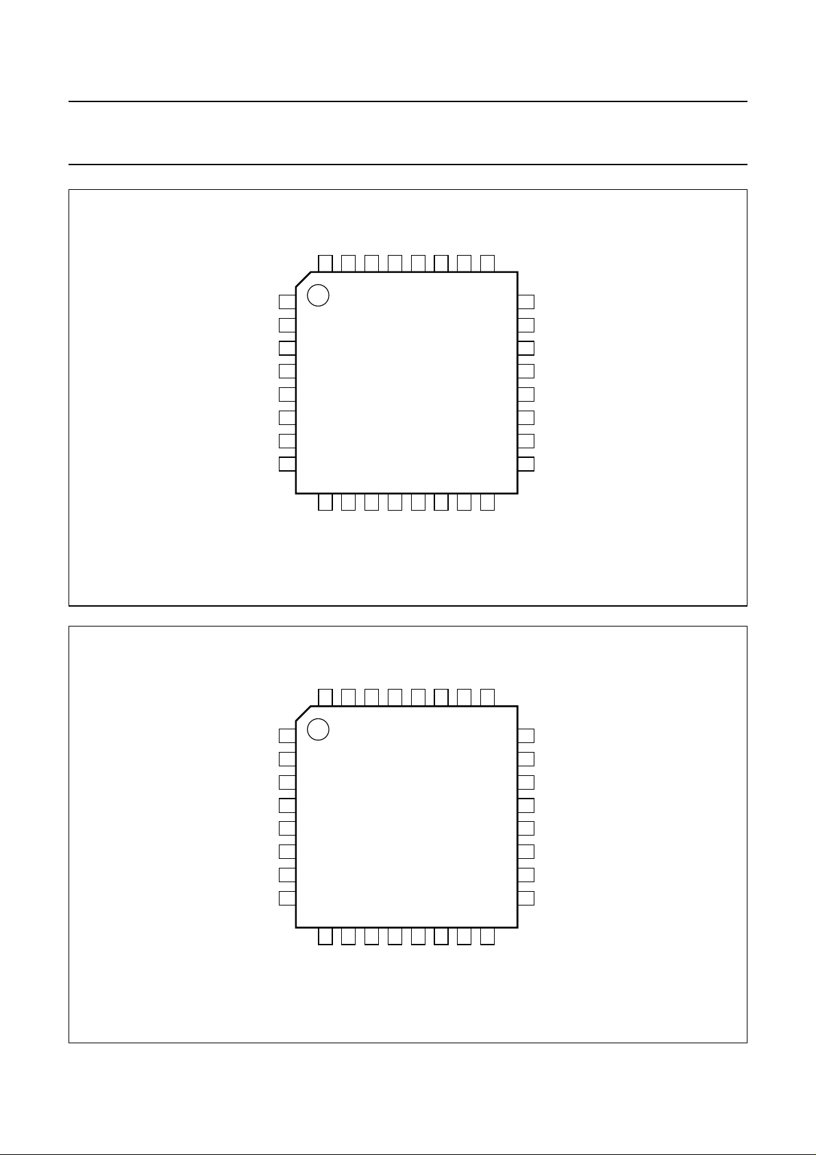
TZA3001BHL
SYMBOL PIN DESCRIPTION
GND 1 ground
MONIN 2 monitor photo diode current input
GND 3 ground
TONE 4 connection for external capacitor
used to set optical ONE control
loop time constant (optional)
TZERO 5 connection for external capacitor
used to set optical ZERO control
loop time constant (optional)
BGAP 6 connection for external band gap
decoupling capacitor
V
CC(G)
GND 8 ground
GND 9 ground
V
CC(B)
GND 11 ground
LAQ 12 inverted laser modulation output
LA 13 laser modulation output
GND 14 ground
BIAS 15 laser bias current output
GND 16 ground
GND 17 ground
V
CC(R)
DLOOP 19 loop mode data input
DLOOPQ 20 loop mode inverted data input
V
CC(R)
ONE 22 optical ONE reference level input
ZERO 23 optical ZERO reference level input
GND 24 ground
GND 25 ground
ENL 26 loop mode enable input
V
CC(R)
DIN 28 data input
DINQ 29 inverted data input
V
CC(R)
ALS 31 automatic laser shutdown input
GND 32 ground
Note to Tables TZA3001AHL and TZA3001BHL
1. See Section “Power supply connections”.
7 supply voltage; note 1
10 supply voltage; note 1
18 supply voltage; note 1
21 supply voltage; note 1
27 supply voltage; note 1
30 supply voltage; note 1
1997 Sep 08 4
Philips Semiconductors Objective specification
SDH/SONET STM4/OC12
laser drivers
handbook, full pagewidth
GND
MONIN
GND
TONE
TZERO
BGAP
V
CC(G)
GND
TZA3001AHL; TZA3001BHL;
TZA3001U
CC(R)
ALS
GND
32
1
2
3
4
5
6
7
8
9
GND
V
31
30
TZA3001AHL
11
10
GND
CC(B)
V
DINQ
29
12
LAQ
DIN
28
13
LA
CC(R)
V
27
14
GND
ALARM
26
15
BIAS
GND
25
16
GND
24
23
22
21
20
19
18
17
MGK273
GND
ZERO
ONE
ALARMLO
V
CC(R)
V
CC(R)
ALARMHI
GND
handbook, full pagewidth
GND
MONIN
GND
TONE
TZERO
BGAP
V
CC(G)
GND
Fig.3 Pin configuration: TZA3001AHL.
CC(R)
ALS
GND
32
1
2
3
4
5
6
7
8
9
GND
V
31
30
TZA3001BHL
11
10
GND
CC(B)
V
DINQ
29
12
LAQ
DIN
28
13
LA
CC(R)
V
27
14
GND
ENL
26
15
BIAS
GND
25
16
GND
24
23
22
21
20
19
18
17
MGK272
GND
ZERO
ONE
V
CC(R)
DLOOPQ
DLOOP
V
CC(R)
GND
Fig.4 Pin configuration: TZA3001BHL.
1997 Sep 08 5

Philips Semiconductors Objective specification
SDH/SONET STM4/OC12
laser drivers
TZA3001AHL; TZA3001BHL;
TZA3001U
PAD CONFIGURATION
TZA3001U (naked die)
COORDINATES
SYMBOL PAD DESCRIPTION
xy
GND 1 ground −664 −910
MONIN 2 monitor photo diode current input −524 −910
GND 3 ground −367 −910
IGM 4 not used (leave unbonded) −227 −910
TONE 5 connection for external capacitor to set optical ONE control loop time
−70 −910
constant (optional)
TZERO 6 connection for external capacitor to set optical ZERO control loop time
+87 −910
constant (optional)
BGAP 7 connection for external band gap decoupling capacitor +244 −910
V
CC(G)
V
CC(G)
8 supply voltage +384 −910
9 supply voltage +524 −910
GND 10 ground +664 −910
GND 11 ground +910 −630
V
V
CC(B)
CC(B)
12 supply voltage +910 −490
13 supply voltage +910 −350
GND 14 ground +910 −210
LAQ 15 inverted laser modulation output +910 −70
LA 16 laser modulation output +910 +70
GND 17 ground +910 +210
BIAS 18 laser bias current output +910 +350
GND 19 ground +910 +490
GND 20 ground +910 +630
GND 21 ground +681 +910
ALARMHI 22 maximum bias current alarm reference level input +541 +910
V
CC(R)
23 supply voltage +384 +910
DLOOP 24 loop mode data input +227 +910
DLOOPQ 25 loop mode inverted data input +87 +910
V
CC(R)
26 supply voltage −70 +910
ALARMLO 27 minimum bias current reference level input −210 +910
ONE 28 optical ONE reference level input −367 +910
ZERO 29 optical ZERO reference level input −524 +910
GND 30 ground −681 +910
GND 31 ground −910 +681
ALARM 32 alarm output −910 +541
ENL 26 loop mode enable input −910 +384
V
CC(R)
34 supply voltage −910 +227
DIN 35 data input −910 +70
(1)
1997 Sep 08 6
 Loading...