

Philips tza1026 DATASHEETS
INTEGRATED CIRCUITS
DATA SH EET
TZA1026
Data amplifier and laser supply
circuit for CD audio and video
optical systems (ADALASAuto)
Product specification
File under Integrated Circuits, IC01
1998 Oct 30

Philips Semiconductors Product specification
Data amplifier and laser supply circuit for CD
audio and video optical systems (ADALASAuto)
FEATURES
• Suitable for automotive applications
• Supports a wide range of voltage output mechanisms
• RF amplifier designed for audio and video applications
with data rates up to a maximum of n = 4 times speed
• Programmable RF gain for CD-Audio/Video (CD-A/V)
and CD-Read/Write (CD-R/W) discs
• Adjustable equalizer for n = 1 or n = 2 times speed
• Fully Automatic Laser Power Control (ALPC) including
stabilization plus a separate laser supply voltage for
power efficiency
• Adjustable current range of ALPC output
• Automatic N- or P-substrate monitor diode selection
• Adjustable laser bandwidth and laser switch-on current
slope using external capacitor
• Protection circuit to prevent laser damage due to laser
supply voltage dip
• Optimized interconnection between data amplifier and
Philips’ digital signal processor CD10Auto (SAA7326)
• Wide supply voltage range
• Power-down switch to reduce power consumption
during standby
• Wide temperature range
• Low power consumption.
GENERAL DESCRIPTION
The TZA1026 is a data amplifier and laser supply circuit for
voltage output mechanisms found in a wide range of audio
and video CD systems. The device contains an RF
amplifier and an automatic laser power control circuit.
The RF bandwidth allows this device to be used in CD-A/V
and CD-R/W applications with a data rate up to a
maximum of n = 4 times speed. The RF gain can be
adapted for CD-A/V discs or CD-R/W discs by means of
the gain select signal.
The equalizer can be adjusted for n = 1 or n = 2 times
speed with the equalizer/speed select signal. For n = 4
times speed the RF is not equalized.
The TZA1026 can be adapted to a wide range of voltage
output mechanisms by means of external resistors.
The ALPC circuit will maintain control over the laser diode
current. With an on-chip reference voltage generator, a
constant and stabilized output power is ensured
independent of ageing. The ALPC can accommodate
N- or P-substrate monitor diodes.
A separate supply voltage connection for the laser allows
the internal power dissipation to be reduced by connecting
a low voltage supply. The laser output current range can
be optimized to fit the requirements of the laser diode by
means of one external resistor. When a DC-to-DC
converter is used, in combination with the control loop of
the ALPC, the adjustable output current range provides
the possibility to compensate for the extra gain a DC-to-DC
converter introduces in the control loop.
TZA1026
The preamplifier forms a versatile, programmable
interface for voltage output CD mechanisms to the Philips’
digital signal processor CD10Auto (SAA7326).
1998 Oct 30 2

Philips Semiconductors Product specification
Data amplifier and laser supply circuit for CD
TZA1026
audio and video optical systems (ADALASAuto)
QUICK REFERENCE DATA
SYMBOL PARAMETER CONDITIONS MIN. TYP. MAX. UNIT
Supplies
V
DD
I
DD
V
DD(L)
RF amplifier
t
d(f)(RF)
Laser supply circuit
I
o(LASER)(max)
V
i(mon)
Temperature range
T
oper
supply voltage 2.7 − 5.5 V
supply current − 3 − mA
laser supply voltage 2.7 − 5.5 V
RF flatness delay EQSEL = LOW; n = 1 −− 10 ns
EQSEL = HIGH; n = 2 −− 5ns
EQSEL = open-circuit;
−− 2.5 ns
n = 4; non equalized
maximum laser output current V
DD(L)
− V
o(LASER)
= 0.55 V 80 −−mA
monitor input voltage
N-substrate monitor diode − 0.150 − V
P-substrate monitor diode − V
− 0.150 − V
DD
operating temperature −40 − +85 °C
ORDERING INFORMATION
TYPE
NUMBER
NAME DESCRIPTION VERSION
PACKAGE
TZA1026T SO14 plastic small outline package; 14 leads; body width 3.9 mm SOT108-1
1998 Oct 30 3
Philips Semiconductors Product specification
Data amplifier and laser supply circuit for CD
audio and video optical systems (ADALASAuto)
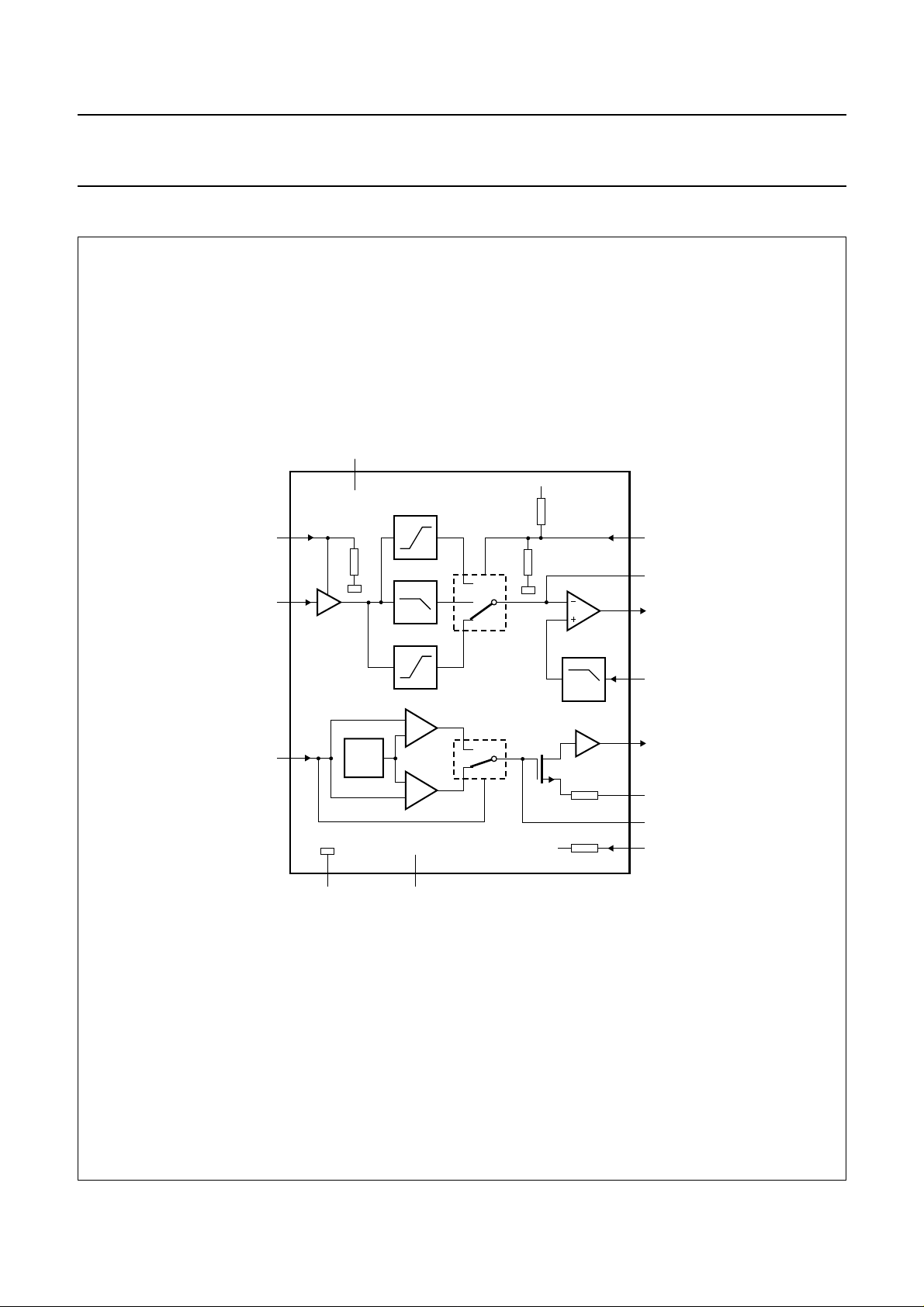
BLOCK DIAGRAM
handbook, full pagewidth
CDRW
DIN
11
5
V
DD
13
1×
4×
TZA1026
V
DD
12
EQSEL
9
RFFB
10
RFEQO
MON
2×
8
250
TZA1026
V/I
4
GND
V
GAP
(1)
V/I
26
V
DD(L)
kHz
V
DD
MBK889
CMFB
1
LD
14
RGADJ
3
CFIL
7
PWRON
(1) Band gap reference voltage.
Fig.1 Block diagram.
1998 Oct 30 4
Philips Semiconductors Product specification
Data amplifier and laser supply circuit for CD
audio and video optical systems (ADALASAuto)
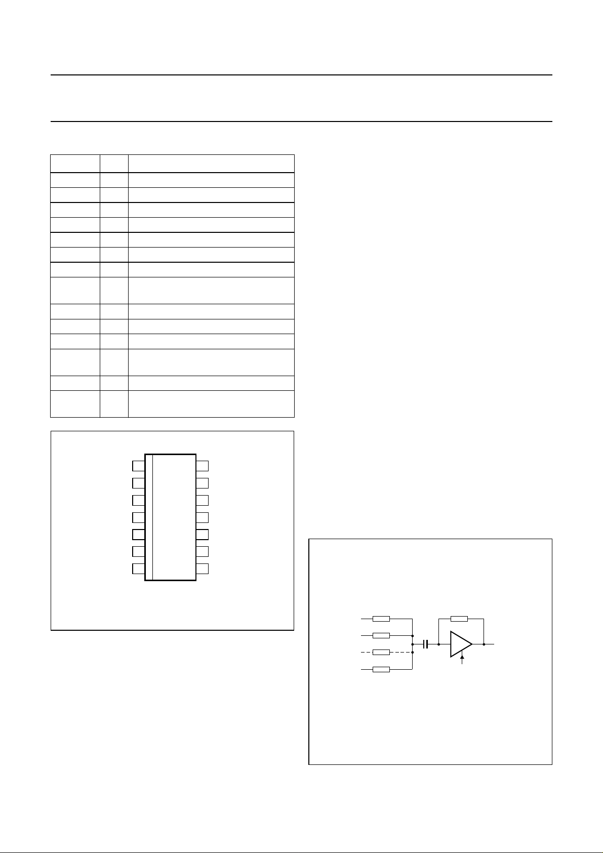
PINNING
SYMBOL PIN DESCRIPTION
LD 1 current output to laser diode
V
DD(L)
2 laser supply voltage
CFIL 3 external filter capacitor
MON 4 laser monitor diode input
DIN 5 central diode input
GND 6 ground
PWRON 7 power-on select input
CMFB 8 common mode feedback voltage
input
RFFB 9 external RF feedback resistor
RFEQO 10 RF amplifier output
CDRW 11 gain select input for CD-A/V, CD-R/W
EQSEL 12 equalizer/speed select input
(n = 1, 2 or 4)
V
DD
13 supply voltage
RGADJ 14 external laser supply gain adjust
resistor
handbook, halfpage
LD
V
DD(L)
CFIL
MON
DIN
GND
PWRON
1
2
3
4
5
6
7
TZA1026
MBK890
14
13
12
11
10
9
8
RGADJ
V
DD
EQSEL
CDRW
RFEQO
RFFB
CMFB
The gain of the RF amplifier can be adjusted by the
external input resistors. Fig.3 shows the simplified
schematic which can be used to determine the RF gain.
The signal is AC coupled to the RF amplifier. The formula
to determine the gain is shown below:
G
RF
where:
G
RF
n is the number of input resistors
Z
tr(RF)
R2 is the value of the input resistors(Ω).
The gain can be increased by a factor 4 by making
pin CDRW HIGH. The value of Z
(CDRW = LOW) and 38 kΩ for CD-R/W (CDRW = HIGH).
The equalizer/bandwidth section can be switched between
n = 1, n = 2 (inclusive the corresponding equalizer) or
n = 4 (inclusive the required bandwidth limitation) times
speed.
The DC output level of the amplifier can be set by applying
a DC voltage on the common mode feedback pin CMFB.
Since the input signal is AC-coupled the RF output voltage
will swing (symmetrically) around this DC level.
The coupling of the TZA1026 to the signal processor
(SAA7326) can be either AC or DC. When an AC-coupling
is chosen (see Fig.8) the minimum supply voltage can be
applied. When a DC-coupling is chosen (see Fig.9) a
minimum supply voltage of 2.8 V is required.
TZA1026
Z
tr RF()
n–
×=
-----------------R2
is the RF amplifier gain
is the transimpedance of the amplifier (Ω)
is 9.8 kΩ for CD-A/V
tr(RF)
(1)
Fig.2 Pin configuration.
FUNCTIONAL DESCRIPTION
The TZA1026 consists of two sections, the RF amplifier
and the automatic laser power control circuit.
RF amplifier
The RF amplifier consists of a current input amplifier, an
equalizer/bandwidth section and a transimpedance output
amplifier with an external feedback resistor of 10 kΩ(fixed
value).
1998 Oct 30 5
handbook, halfpage
V
in
V
in
V
in
R2(1)
R2(2)
R2(n)
10 kΩ
C2
CDRW
Fig.3 Simplified schematic.
RFEQO
MGL530
Philips Semiconductors Product specification
Data amplifier and laser supply circuit for CD
audio and video optical systems (ADALASAuto)
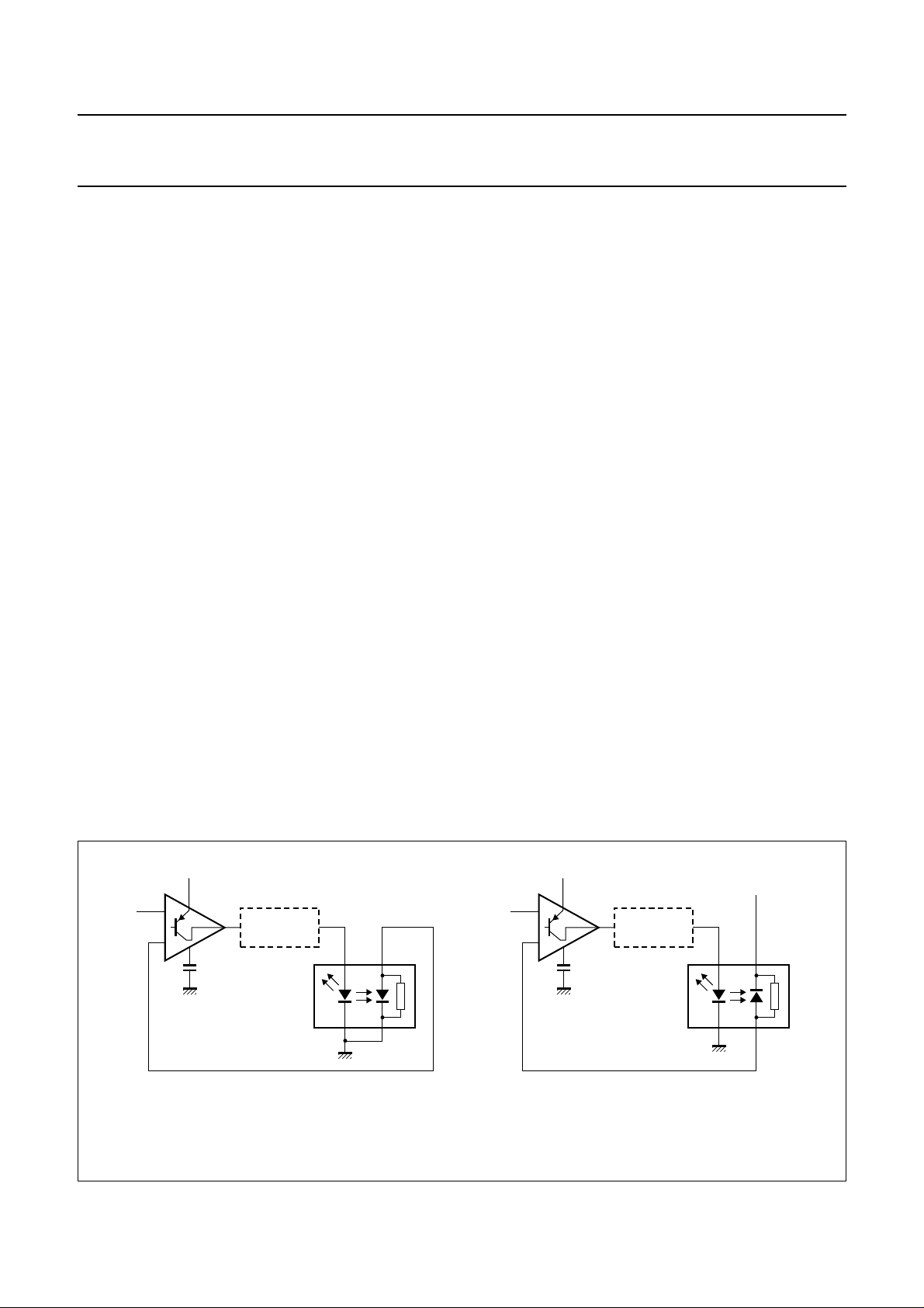
Automatic laser power control circuit
The ALPC stabilises the laser output power thereby
reducing the effect of ageing of the laser.
The TZA1026 automatically detects when an
N- or P-substrate monitor diode is used and selects the
correct reference voltage. A simplified diagram for the use
of an N- or P-substrate monitor diode is given in Fig.4.
The gain of the loop can be controlled (reduced) by adding
an external resistor between pins RGADJ and GND.
The loop gain then becomes:
G
loop
G
ALPCGlm
× G
×
con
250
×=
------------------------------------250 R
+
RGADJ
where:
G
is the loop gain
loop
G
is the ALPC transfer (60 A/V)
ALPC
Glm is the laser-to-monitor transfer (V/A)
G
is the extra gain introduced when a DC-to-DC
con
converter is used in the loop; G
= 1 when no
con
DC-to-DC converter is used
250 is a fixed internal resistor value (Ω)
R
is the value of the external resistor (Ω).
RGADJ
The minimum available output current is also reduced
when an external resistor is used. The formula to
determine the minimum available output current is shown
in equation (3).
I
oIo(LASER)(max)
250
×=
------------------------------------250 R
+
RGADJ
where:
is output current (mA)
I
o
I
o(LASER)(max)
250 is a fixed internal resistor value (Ω)
R
RGADJ
The bandwidth of the loop is determined by the external
filter capacitor C
determine the bandwidth is shown in equation (4).
τ
=
-3dB
(2)
where:
C
CFIL
G
loop
The TZA1026 has a protection circuit to prevent laser
damage that can occur due to a dip of V
occurs the output transistor (see Fig.4) will go into
saturation making it unable to supply the required laser
current. Without the protection circuit the ALPC would still
try to supply the required laser current by charging the filter
capacitor C
would create a large output current during the few
milliseconds it needs to discharge the capacitor to a
normal level. The protection circuit monitors the output
transistor and switches off the ALPC when saturation
occurs by discharging the capacitor. The ALPC will
automatically restart within a few milliseconds after the dip
(3)
has passed.
TZA1026
is the maximum laser output current (mA)
is the value of the external resistor (Ω).
and the loop gain. The formula to
CFIL
C
----------------------------------------- -
is the value of the capacitor (F)
is the loop gain.
16 106⋅×
CFIL
G
loop
DD(L)
. After the dip a fully charged capacitor
CFIL
(4)
. When a dip
handbook, full pagewidth
150 mV
V
DD(L)
C
CFIL
DC-TO-DC
CONVERTER
a. N-substrate monitor diode. b. P-substrate monitor diode.
Fig.4 Automatic Laser Power Control (ALPC) loop.
1998 Oct 30 6
VDD − 150 mV
V
DD(L)
C
CFIL
DC-TO-DC
CONVERTER
V
DD
MGR519
 Loading...